WO2012002368A1 - アレイ導波路回折格子型光合分波器 - Google Patents
アレイ導波路回折格子型光合分波器 Download PDFInfo
- Publication number
- WO2012002368A1 WO2012002368A1 PCT/JP2011/064769 JP2011064769W WO2012002368A1 WO 2012002368 A1 WO2012002368 A1 WO 2012002368A1 JP 2011064769 W JP2011064769 W JP 2011064769W WO 2012002368 A1 WO2012002368 A1 WO 2012002368A1
- Authority
- WO
- WIPO (PCT)
- Prior art keywords
- waveguide
- arrayed
- chip
- arrayed waveguide
- demultiplexer
- Prior art date
Links
Images


Classifications
-
- G—PHYSICS
- G02—OPTICS
- G02B—OPTICAL ELEMENTS, SYSTEMS OR APPARATUS
- G02B6/00—Light guides; Structural details of arrangements comprising light guides and other optical elements, e.g. couplings
- G02B6/10—Light guides; Structural details of arrangements comprising light guides and other optical elements, e.g. couplings of the optical waveguide type
- G02B6/12—Light guides; Structural details of arrangements comprising light guides and other optical elements, e.g. couplings of the optical waveguide type of the integrated circuit kind
- G02B6/12007—Light guides; Structural details of arrangements comprising light guides and other optical elements, e.g. couplings of the optical waveguide type of the integrated circuit kind forming wavelength selective elements, e.g. multiplexer, demultiplexer
- G02B6/12009—Light guides; Structural details of arrangements comprising light guides and other optical elements, e.g. couplings of the optical waveguide type of the integrated circuit kind forming wavelength selective elements, e.g. multiplexer, demultiplexer comprising arrayed waveguide grating [AWG] devices, i.e. with a phased array of waveguides
- G02B6/12026—Light guides; Structural details of arrangements comprising light guides and other optical elements, e.g. couplings of the optical waveguide type of the integrated circuit kind forming wavelength selective elements, e.g. multiplexer, demultiplexer comprising arrayed waveguide grating [AWG] devices, i.e. with a phased array of waveguides characterised by means for reducing the temperature dependence
- G02B6/1203—Light guides; Structural details of arrangements comprising light guides and other optical elements, e.g. couplings of the optical waveguide type of the integrated circuit kind forming wavelength selective elements, e.g. multiplexer, demultiplexer comprising arrayed waveguide grating [AWG] devices, i.e. with a phased array of waveguides characterised by means for reducing the temperature dependence using mounting means, e.g. by using a combination of materials having different thermal expansion coefficients
Definitions
- the present invention relates to an arrayed waveguide diffraction grating type optical multiplexer / demultiplexer having a function of a wavelength multiplexer / demultiplexer that combines light of different wavelengths into one or separates each wavelength, and in particular, athermalization (temperature independence).
- the present invention relates to an arrayed waveguide grating optical multiplexer / demultiplexer.
- AWG arrayed Waveguide Grating
- quartz glass which plays an important role as a wavelength multiplexer / demultiplexer (multiplexing / demultiplexing)
- the refractive index of light in quartz glass is temperature-dependent. Temperature dependence also occurs in the wavelength (transmission center wavelength).
- the temperature dependence of the center wavelength of an AWG made of quartz glass is 0.011 nm / ° C, which is a large value that cannot be ignored for use in a D-WDM (Dense-Wavelength Division Multiplexing) transmission system. ing.
- AWG is strongly required to be athermal (temperature independent) that does not require a power source.
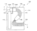
- An arrayed waveguide diffraction grating type optical multiplexer / demultiplexer (athermal AWG module) which is athermalized using a compensation plate is described in Patent Document 1 (see FIG. 14).
- An arrayed waveguide diffraction grating type optical multiplexer / demultiplexer 100 shown in FIG. 14 includes a first waveguide 102 formed in a waveguide chip 114, a first slab waveguide 104 connected to the first waveguide 102, 2 waveguide 106, a second slab waveguide 108 connected to the second waveguide 106, and an arrayed waveguide 110 connecting the first slab waveguide 104 and the second slab waveguide 108.
- This arrayed waveguide diffraction grating type optical multiplexer / demultiplexer 100 is cut into two at the first slab waveguide 104 portion, the input side portion 116 including a part 104A of the first slab waveguide 104, and the first slab waveguide. It is divided into an output side portion 118 including the other portion 104B of the waveguide 104.
- the input side portion 116 and the output side portion 118 are connected by a compensation plate 112.
- the compensation plate 112 expands and contracts to move the portion 104A of the first slab waveguide 104, thereby correcting the wavelength shifted by the temperature change.
- An object of the present invention is to provide an arrayed waveguide diffraction grating type optical multiplexer / demultiplexer that can stably obtain a low noise level even if the temperature changes in consideration of the above facts.
- the invention according to the first aspect of the present invention includes at least one first waveguide, a first slab waveguide connected to the first waveguide, and the first waveguide in the first slab waveguide.
- One end is connected to the side opposite to the side to which the two are connected, an arrayed waveguide comprising a plurality of channel waveguides having different lengths and curved in the same direction, and the other of the arrayed waveguides
- a second slab waveguide connected to an end of the second slab waveguide, and a plurality of second waveguides connected in parallel to each other on the opposite side of the second slab waveguide from the side to which the arrayed waveguide is connected.
- a waveguide chip that is divided into a first separation waveguide chip and a second separation waveguide chip in any one of the first slab waveguide and the second slab waveguide; Supports the first isolation waveguide chip A first base for supporting the second separation waveguide chip, a second base for supporting the second separation waveguide chip, and the first and second separation waveguide chips by expanding and contracting according to a temperature change.
- a compensation member that compensates for a temperature-dependent shift of a light transmission center wavelength of the arrayed waveguide grating in the waveguide chip by shifting a relative position, and the first separation waveguide chip includes the array
- the second separation waveguide chip is fixed to the first base in at least a part of a region not including the waveguide, and the second separation waveguide chip is formed in the first part in the region not including the arrayed waveguide.
- the present invention relates to an arrayed waveguide grating type optical multiplexer / demultiplexer characterized by being fixed to two bases.
- the portion of the arrayed waveguide is not fixed to any of the first and second bases.
- a low noise level can be stably obtained even when the value of f is changed.
- the invention according to the second aspect of the present invention relates to an arrayed waveguide diffraction grating type optical multiplexer / demultiplexer in which a portion of the arrayed waveguide in the first and second bases is cut away.
- the portion of the first and second bases where the arrayed waveguide is not fixed is cut out, so that it is easy.
- the invention according to a third aspect of the present invention relates to the arrayed waveguide analysis grating type optical multiplexer / demultiplexer according to the description, wherein the boundary portion of the waveguide chip divided into two is sandwiched in the thickness direction by a clip. .
- the waveguide chip is sandwiched in the thickness direction by a clip at the divided portion of the divided arrayed waveguide grating. Therefore, when the arrayed waveguide grating divided into two is moved relative to each other by the expansion and contraction of the compensation member without being affected by the dimension error in the thickness direction of the two bases. It is possible to prevent the deviation in the thickness direction between the two waveguide chips.
- the invention according to a fourth aspect of the present invention relates to an arrayed waveguide grating optical multiplexer / demultiplexer in which openings for positioning the clips are formed on the first and second bases.
- two positions are obtained by aligning the positions of the openings and the clips provided in the first and second bases. It is easy to align the position of the clip with the divided portion of the arrayed waveguide diffraction grating divided into two.
- an arrayed waveguide diffraction grating type optical multiplexer / demultiplexer that can stably obtain a low noise level even if the temperature changes.
- FIG. 1A is a plan view showing a configuration of an arrayed waveguide grating optical multiplexer / demultiplexer according to Embodiment 1.
- FIG. 1B is a side view showing the configuration of the arrayed waveguide grating optical multiplexer / demultiplexer according to the first embodiment.
- FIG. 2A is a plan view showing a configuration of an arrayed waveguide grating optical multiplexer / demultiplexer according to the second embodiment.
- FIG. 2B is a side view showing the configuration of the arrayed waveguide grating optical multiplexer / demultiplexer according to the second embodiment.
- FIG. 1A is a plan view showing a configuration of an arrayed waveguide grating optical multiplexer / demultiplexer according to Embodiment 1.
- FIG. 1B is a side view showing the configuration of the arrayed waveguide grating optical multiplexer / demultiplexer according to the first embodiment.
- FIG. 2A is a plan view
- FIG. 3A is a plan view showing a configuration of an arrayed waveguide grating optical multiplexer / demultiplexer according to the third embodiment.
- FIG. 3B is a side view showing the configuration of the arrayed waveguide grating optical multiplexer / demultiplexer according to the third embodiment.
- FIG. 4 is a cross-sectional view in the thickness direction showing the configuration of the portion sandwiched by the clips in the arrayed waveguide grating optical multiplexer / demultiplexer according to the first or third embodiment.
- FIG. 5A is a plan view illustrating a configuration of an arrayed waveguide grating optical multiplexer / demultiplexer according to the fourth embodiment.
- FIG. 5B is a side view illustrating the configuration of the arrayed waveguide grating optical multiplexer / demultiplexer according to the fourth embodiment.
- FIG. 6 is an explanatory view showing a plurality of waveguide chips formed on the wafer.
- FIG. 7 is an explanatory diagram showing a case where individual waveguide chips are cut out from a wafer on which a plurality of waveguide chips are formed.
- FIG. 8 is a plan view showing the configuration of individual waveguide chips cut out from the wafer.
- FIG. 9 is a table showing circuit parameters of the arrayed waveguide used for determining the length of the compensation plate of the arrayed waveguide grating optical multiplexer / demultiplexer according to the first embodiment.
- FIG. 9 is a table showing circuit parameters of the arrayed waveguide used for determining the length of the compensation plate of the arrayed waveguide grating optical multiplexer / demultiplexer according to the first embodiment.
- FIG. 10 is a graph showing changes in the center wavelength when a temperature history is given to the arrayed waveguide grating optical multiplexer / demultiplexer according to the first embodiment in which the compensation member is bonded on the extension line.
- FIG. 11 is a graph showing the evaluation results of the temperature characteristics of the arrayed waveguide grating optical multiplexer / demultiplexer according to the first embodiment.
- FIG. 12 is a graph showing the loss wavelength characteristic and temperature change of the arrayed waveguide analysis grating type optical multiplexer / demultiplexer according to the first embodiment.
- FIG. 13 is a graph showing the loss wavelength characteristic and temperature change of the arrayed waveguide analysis grating type optical multiplexer / demultiplexer in Comparative Example 1.
- FIG. 11 is a graph showing the evaluation results of the temperature characteristics of the arrayed waveguide grating optical multiplexer / demultiplexer according to the first embodiment.
- FIG. 12 is a graph showing the loss wavelength characteristic and temperature change of the arraye
- FIG. 14 is a plan view showing the configuration of an example of a conventional arrayed waveguide diffraction grating type optical multiplexer / demultiplexer.
- 15A is a plan view showing a configuration of an arrayed waveguide grating optical multiplexer / demultiplexer used in Comparative Example 1.
- FIG. 15B is a side view showing the configuration of the arrayed waveguide grating optical multiplexer / demultiplexer used in Comparative Example 1.
- Embodiment 1 Hereinafter, an example of an arrayed waveguide grating optical multiplexer / demultiplexer according to the present invention will be described.
- FIG. 1A is a plan view of an arrayed waveguide grating optical multiplexer / demultiplexer 1 according to Embodiment 1
- FIG. 1B is a side view thereof.
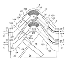
- the arrayed waveguide grating optical multiplexer / demultiplexer 1 according to the first embodiment has one waveguide chip 16 having a substantially boomerang type planar shape.
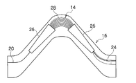
- the waveguide chip 16 includes a substrate 12 made of silicon and an arrayed waveguide diffraction grating 14 formed on the substrate 12.
- the arrayed waveguide diffraction grating 14 includes at least one first waveguide 20, a first slab waveguide 22 connected to the first waveguide 20, and the first waveguide 20 in the first slab waveguide 22. One end is connected to the side opposite to the side where the two are connected, an array waveguide 28 composed of a plurality of channel waveguides 28a, and a second slab waveguide 26 connected to the other end of the array waveguide 28
- the second slab waveguide 26 includes a second waveguide 24 connected in a state of being arranged in parallel on the side opposite to the arrayed waveguide 28.
- the arrayed waveguide diffraction grating 14 is an optical waveguide made of a core and a clad formed on a silicon substrate 12 by combining a flame deposition method (FHD method), an optical fiber manufacturing technology, and a semiconductor microfabrication technology.
- FHD method flame deposition method
- PLC Planar Lightwave Circuit
- the channel waveguides 28a constituting the arrayed waveguides 28 have different lengths, and are arranged in order from the shortest to the longest from one side edge of the waveguide chip 16 to the other side edge.
- the arrayed waveguide 28 has a shape that bends in a specific direction as shown in FIG. 1A.
- the waveguide chip 16 is cut in a curved shape along the contour of the arrayed waveguide diffraction grating 14 and has a shape (boomerang shape) bent along the bending direction of the arrayed waveguide 28.
- the first slab waveguide 22 is divided together with the substrate 12 by a cut surface 30 which is a vertical surface intersecting the optical axis. Therefore, the arrayed waveguide grating 14 is also divided into two by the cut surface 30.
- the waveguide chip 16 is divided into the first separation waveguide chip 16A and the second separation waveguide chip 16B by the cut surface 30, respectively. Further, in each waveguide chip 16, the first slab waveguide 22 is divided into two parts, that is, a first separation slab waveguide 22 ⁇ / b> A and a second separation slab waveguide 22 ⁇ / b> B by the cut surface 30. Note that the waveguide chip 16 may be cut by the second slab waveguide 26 instead of being cut by the first slab waveguide 22.
- the first separation slab waveguide 22A refers to the side of the first slab waveguide 22 divided into two, to which the first waveguide 20 is connected, and the second separation slab waveguide 22B is an array conductor. This is the side to which the waveguide 28 is connected.
- the first separation waveguide chip 16A is the side including the first separation slab waveguide 22A among the two divided waveguide chips 16, and the second separation waveguide chip 16B is the first separation waveguide chip 16B. 2 is a side provided with two separate slab waveguides 22B.
- the substrate on which the first separation waveguide chip 16A is fixed is called the first substrate 12A
- the second separation waveguide chip 16B is the second separation waveguide chip 16B.
- the formed substrate is referred to as a second substrate 12B.
- the first substrate 12A and the second substrate 12B have a necessary amount of relative position change in a desired direction between one and the other of the arrayed waveguide grating 14 divided into two by the cut surface 30. What is necessary is just to be formed. Therefore, the first substrate 12A and the second substrate 12B may not be completely separated but may be partially connected.
- the first separation waveguide chip 16A is a first glass plate 32 as an example of the first base of the present invention
- the second separation waveguide chip 16B is a second one of the present invention.
- Each is fixed to a second glass plate 34 as an example of a base.
- the second separation waveguide chip 16B is bonded and fixed to the second glass plate 34 at, for example, the second slab waveguide 26 and the second waveguide 24 other than the portion where the arrayed waveguide 28 is formed.
- the first glass plate 32 and the second glass plate 34 have a shape in which a portion to support the arrayed waveguide 28 is cut out.
- the portion of the arrayed waveguide 28 in the arrayed waveguide diffraction grating 14 is not fixed to either the first glass plate 32 or the second glass plate 34. Since both the first glass plate 32 and the second glass plate 34 are made of quartz glass, ultraviolet rays can pass through the base, and the first separation waveguide chip 16A and the first glass plate can be transmitted. 32, and an ultraviolet curable adhesive can be used for bonding the second separation waveguide chip 16B and the second glass plate 34 to each other.
- the portion of the waveguide chip 16 where the arrayed waveguides 28 are formed is not bonded and fixed, so that a low noise level can be stably obtained even when the temperature changes.
- the second glass plate 34 having a shape in which a portion to support the arrayed waveguide 28 is cut out is used.
- a portion to support the arrayed waveguide 28 is not cut out.
- the same effect can be obtained if it is not bonded or fixed.
- the cost can be reduced and the management of the adhesive can be facilitated, thus facilitating the work.
- the waveguide chip 16 has a planar shape curved with the same curvature in the same direction as the curved direction of the arrayed waveguide. Therefore, it can be configured more compactly than an arrayed waveguide diffraction grating type optical multiplexer / demultiplexer having a waveguide chip having a rectangular outer shape.
- the arrayed waveguide grating-side optical multiplexer / demultiplexer 1 straddles the first glass plate 32 and the second glass plate 34, and one side is fixed to the upper surface of the first glass plate 32 with an adhesive, A rectangular compensation member 18 whose other side is fixed to the upper surface of the second first glass plate 32 with an adhesive is provided.
- the compensation member 18 is arranged such that its long side (longitudinal direction) is parallel to the extending direction of the cut surface 30.
- the compensation member 18 uses a metal plate made of copper or pure aluminum (JIS: A1050). As shown in FIG.
- leg portions 18A project from both ends of the compensation member 18, and the leg portions 18A are fixed to the first glass plate 32 and the second glass plate 34 with an adhesive. .
- the adhesion area of the 1st glass plate 32 and the 2nd glass plate 34, and the compensation member 18 is made constant. Note that if the adhesion area is different, the effective length may change and the temperature characteristics may vary.
- the length of the compensation member 18 is calculated by the following (Equation 1) and the circuit parameters of the arrayed waveguide grating 14 shown in FIG. 9, and is 18 mm in this embodiment.
- the condensing position by the first slab waveguide 22 changes by dx.
- the compensation member 18 expands and contracts by dx due to a change in temperature, so that the first glass plate 32 and the second glass plate 34 move relative to each other along the cut surface 30.
- the separation slab waveguide 22A also moves relative to the separation slab waveguide 22B along the cut surface 30.
- a wavelength multiplexed optical signal in which optical signals having different wavelengths are superimposed is input to the first waveguide 20, or a wavelength multiplexed signal is output from the first waveguide 20.
- the first slab waveguide 22 has a function of demultiplexing the wavelength multiplexed optical signal input from the first waveguide 20 for each wavelength and a function of multiplexing the optical signals of different wavelengths propagated through the arrayed waveguide 28. Have.
- the arrayed waveguide 28 has a function of propagating an optical signal for each wavelength, and has a number corresponding to the number of channels of the wavelength multiplexed optical signal input to the first waveguide 20, for example, 100 channel waveguides 28a. They are provided at a predetermined pitch d.
- the pitch d of the channel waveguide 28a is 13.8 ⁇ m, but the pitch d is not limited to this length.
- the channel waveguides 28a have different lengths corresponding to the wavelengths of the propagated light. Therefore, as described above, the lengths of the two adjacent channel waveguides 28a differ from each other by the set amount ⁇ L.
- the set amount ⁇ L is set to 31.0 ⁇ m as shown in FIG.
- the portion cut by the cut surface 30 of the waveguide chip 16 is sandwiched by the contact plate 15 from both sides.
- the clip 17 may be clamped from above the backing plate 15.
- FIG. 4 shows a cross section (XX cross section in FIG. 1A) cut in the thickness direction along the cut surface 30.
- the portion cut by the cut surface 30 of the waveguide chip 16 is sandwiched between the contact plates 15 from both sides, and is sandwiched by the clips 17 from the top of the contact plate 15.
- a groove 15 ⁇ / b> A is formed in the central portion of the contact plate 15 along the optical axis of the first slab waveguide 22.
- the clip 17 has a substantially U-shaped cross section, and the opening side end portion 17A bent inward so as to face each other and the spring portion that urges the opening side end portion 17A in a direction close to each other. 17B.
- the end of the opening-side end portion 17A of the clip 17 is formed so as to engage with a groove 15A formed in the backing plate 15.
- a predetermined number of arrayed waveguide diffraction gratings 14 are condensed and formed on a single silicon silicon wafer 11.
- the silicon wafer 11 on which the arrayed waveguide diffraction grating 14 is formed is cut into a curved shape along a cutting line 38 using a laser processing machine (for example, a CO 2 laser).
- a laser processing machine for example, a CO 2 laser.
- the waveguide chip 16 is cut along the first slab waveguide 22 together with the substrate 12 in a direction orthogonal to the optical axis (center line) of the first slab waveguide 22. This is divided into two parts, one separation waveguide chip 16A (see FIG. 1A) and a second separation waveguide chip 16B (see FIG. 1A).
- the first separation waveguide chip 16A thus obtained is bonded and fixed to the first glass plate 32, and the second separation waveguide chip 16B is bonded to the second glass plate 34.
- the compensation member 18 is attached so that the center wavelength of the arrayed waveguide grating 14 matches the wavelength of the ITU-T grid.
- one leg 18A of the compensation member 18 is fixed to the upper surface of the first glass plate 32 with an adhesive so that the long side of the compensation member 18 is parallel to the extending direction of the cut surface 30.
- the other leg 18A is fixed to the upper surface of the second first glass plate 32 with an adhesive.
- a plurality of optical signals ( ⁇ 1 to ⁇ n) having different wavelengths are used in the waveguide chip 16 as indicated by an arrow A in FIG. 1A. ) Are individually input from each second waveguide 24.
- the input optical signals ( ⁇ 1 to ⁇ n) are individually input to each channel waveguide 28a in the arrayed waveguide diffraction grating 14 through the second slab waveguide 26.
- optical signals ( ⁇ 1 to ⁇ n) propagated through the channel waveguides 28a are multiplexed by the first slab waveguide 22 and output from the first waveguide 20 as wavelength multiplexed optical signals as indicated by an arrow B in FIG. 1A. Is done.
- the condensing position in the first slab waveguide 22 (the condensing position of the first slab waveguide 22 by the second separation slab waveguide 22B) changes, but is indicated by an arrow J in FIG. 1A.
- the first separation slab waveguide 22A moves relative to the separation slab waveguide 22B by the expansion and contraction of the compensation member 18 to correct the condensing position. For this reason, even if the temperature changes, an optical signal having the same wavelength can be extracted from the first waveguide 20.
- the wavelength multiplexed optical signal in which a plurality of optical signals having the same wavelengths ( ⁇ 1 to ⁇ n) as the input optical signals ( ⁇ 1 to ⁇ n) are multiplexed is the first.
- the arrayed waveguide grating optical multiplexer / demultiplexer 1 is used for demultiplexing (DEMUX)
- a plurality of optical signals ( ⁇ 1) having different wavelengths are used in the waveguide chip 16 as indicated by an arrow C in FIG. 1A.
- ⁇ n is multiplexed from the first waveguide 20.
- the input wavelength multiplexed signal is demultiplexed into n optical signals having wavelengths ( ⁇ 1, ⁇ 2, ⁇ 3,..., ⁇ n) in the first slab waveguide 22, and individually input to each channel waveguide 28a. Is done.
- the optical signals individually propagated through the channel waveguides 28a are individually output from the second waveguides 24 through the second slab waveguides 26 as indicated by arrows D in FIG. 1A. That is, in the arrayed waveguide grating 14, a wavelength-multiplexed optical signal in which a plurality of optical signals ( ⁇ 1 to ⁇ n) having different wavelengths are multiplexed is input from the first waveguide 20, and is demultiplexed for each wavelength to be second. Output from the waveguide 24.
- the condensing position in the first separation slab waveguide 22A of the first slab waveguide 22 changes, but the first separation slab waveguide 22A becomes the second separation by the expansion and contraction of the compensation member 18.
- the light collection position is corrected by moving relative to the slab waveguide 22B. For this reason, even if the temperature changes, an optical signal having the same wavelength is extracted from one second waveguide 24. That is, optical signals having the same wavelengths as the wavelengths ⁇ 1 to ⁇ n in the input wavelength multiplexed optical signal are individually output from the second waveguides 24.
- the compensation member 18 is fixed to the first glass plate 32 and the second glass plate 34 in order to fix the compensation member 18 to the waveguide chip 16.
- the shapes of the first separation waveguide chip 16A and the second separation waveguide chip 16B can be determined without considering the above.
- the planar shape of the waveguide chip 16 is generally a boomerang that is curved with the same bending direction and curvature as the arrayed waveguide diffraction grating 14. Therefore, the package size can be the same as or smaller than the arrayed waveguide grating type optical multiplexer / demultiplexer in which the planar shape of the waveguide chip is rectangular.
- a plurality of arrayed waveguide diffraction gratings 14 formed on one silicon wafer 11 are cut into a curved shape along the outline of each arrayed waveguide diffraction grating 14 using a laser processing machine. Since the outer shape of the waveguide chip 16 has a substantially boomerang shape, the number of waveguide chips 16 per silicon wafer 11 can be increased more than when the waveguide chip 16 has a rectangular shape.
- the waveguide chip 16 is cut at the first slab waveguide 22 in a direction orthogonal to the optical axis (center line) by the cut surface 30, and the long side of the compensation member 18 is the cut surface 30.
- the separation slab waveguide 22A moves relative to the separation slab waveguide 22B along the cut surface 30 by being fixed to the first glass plate 32 and the second glass plate 34 so as to be parallel to the longitudinal direction. To do. In this way, by moving the divided separation slab waveguide 22A relative to the separation slab waveguide 22B along the cut surface 30, the condensing position of the first slab waveguide 22 can be corrected with high accuracy. it can.
- the outer shape of the waveguide chip 16 into a boomerang shape, there is no cut line remaining in the chip as compared with the case of cutting using a dicing apparatus, so that the mechanical characteristics of the waveguide chip 16 with respect to shock and vibration are not limited. Can be improved.
- the first separation waveguide chip 16A and the second separation waveguide chip 16B are sandwiched in the thickness direction between the contact plate 15 and the clip 17 at the dividing surface 30, that is, the boundary between the two.
- the compensation member 18 expands and contracts, the first separation waveguide chip 16A and the second separation waveguide chip 16B are moved when the first separation waveguide chip 16A moves relative to the second separation waveguide chip 16B. It is possible to prevent the deviation in the thickness direction from occurring between the two. Further, the first glass plate 32 and the second glass plate 34 are not affected by dimensional errors in the thickness direction.
- Embodiment 2 Hereinafter, another example of the arrayed waveguide diffraction grating type optical multiplexer / demultiplexer according to the present invention will be described.
- FIG. 2A is a plan view of the arrayed waveguide grating optical multiplexer / demultiplexer 2 according to the second embodiment
- FIG. 2B is a side view thereof.
- two waveguide chips 16 are arranged in parallel.
- the configuration of the waveguide chip 16 is the same as that of the first embodiment.
- the number of waveguide chips 16 is not limited to two, and may be three or more.
- each of the waveguide chips 16 is cut at one cut surface 30 at a portion of the first slab waveguide 22 in the arrayed waveguide diffraction grating 14 to be separated from the first separated waveguide chip 16A and the second waveguide chip 16A.
- the separated waveguide chip 16B Therefore, the first slab waveguide 22 is also separated by the cut surface 30 into the first separated slab waveguide 22A and the second separated slab waveguide 22B.
- the first separation waveguide chip 16A is bonded to the common first glass plate 32
- the second separation waveguide chip 16B is bonded to the common second glass plate 34, respectively. It is fixed.
- the second separation waveguide chip 16 ⁇ / b> B is bonded and fixed to the second glass plate 34 at a portion other than the arrayed waveguide 28 in the arrayed waveguide diffraction grating 14. Further, the portion of the arrayed waveguide 28 in the second separation waveguide chip 16B is not fixed to either the first glass plate 32 or the second glass plate 34.
- the arrayed waveguide grating optical multiplexer / demultiplexer 2 has the following features in addition to the features of the arrayed waveguide grating optical multiplexer / demultiplexer 1 according to the first embodiment.
- temperature compensation can be performed on the two waveguide chips 16 by one common compensation member 18.
- the arrayed waveguide diffraction grating type optical multiplexer / demultiplexer 2 has a plurality of waveguide chips 16, but the waveguide chips 16 are reduced to 1. It can be formed in the same area as the arrayed waveguide diffraction grating type optical multiplexer / demultiplexer 1 of the first embodiment having only one.
- the package size can be reduced to be equal to or smaller than the current product.
- the waveguide chips 16 can all have the same configuration, and since only one compensation member 18 is required, it is easy to share parts, and cost merit is easily obtained.
- Embodiment 3 Hereinafter, still another example of the arrayed waveguide grating optical multiplexer / demultiplexer according to the present invention will be described.
- FIG. 3A is a plan view of an arrayed waveguide grating optical multiplexer / demultiplexer 3 according to Embodiment 3, and FIG. 3B is a side view thereof.
- FIG. 4 shows a cross section (XX cross section in FIG. 3A) cut in the thickness direction along the cut surface 30.
- the arrayed waveguide diffraction grating type optical multiplexer / demultiplexer 3 according to the third embodiment is applied to the portion cut by the cut surface 30 of the waveguide chip 16 from both sides as shown in FIG. It is sandwiched between the plates 15 and sandwiched by the clips 17 from above the backing plate 15.
- the second glass plate 34 is cut out at a portion corresponding to the arrayed waveguide 28, and is opposed to the first glass plate 32 in a substantially inverted letter shape.
- a rectangular opening 19 is formed in a portion corresponding to the cut surface 30 of the first slab waveguide 22.
- the protrusion part 33 and the protrusion part 35 are formed in the 1st glass plate 32 and the 2nd glass plate 34, and the rectangular-shaped opening part 19 is the protrusion part 33, the 1st glass plate 32, and The protrusion 35 and the second glass plate 34 are formed. Then, the positioning between the contact plate 15 and the clip 17 is performed by the opening 19.
- the arrayed waveguide grating optical multiplexer / demultiplexer 3 has the same configuration as the arrayed waveguide grating optical multiplexer / demultiplexer 1 of the first embodiment.
- the arrayed waveguide diffraction grating side optical multiplexer / demultiplexer 3 has the following features in addition to the features of the arrayed waveguide diffraction grating type optical multiplexer / demultiplexer 1 according to the first embodiment. That is, in the arrayed waveguide diffraction grating type optical multiplexer / demultiplexer 3, by aligning the positions of the opening 19, the contact plate 15, and the clip 17, the divided portion of the arrayed waveguide diffraction grating 14 divided into two is provided. It is easy to align the positions of the contact plate 15 and the clip 17.
- Embodiment 4 hereinafter, still another example of the arrayed waveguide grating optical multiplexer / demultiplexer according to the present invention will be described.
- FIG. 5A is a plan view of an arrayed waveguide grating optical multiplexer / demultiplexer 4 according to Embodiment 4, and FIG. 5B is a side view thereof.
- the second glass plate 34 is not cut out at a portion corresponding to the arrayed waveguide 28. It is formed on almost the entire surface corresponding to the waveguide chip 16B. However, a cut portion 37 is formed in the portion of the second glass plate 34 corresponding to the second slab waveguide 26 so as to cross the second slab waveguide 26. In the second separation waveguide chip 16B, only the portion near the second waveguide 24 is bonded to the second glass plate 34 with the notch 37 in the portion where the second slab waveguide 26 is formed as a boundary. The portion where the arrayed waveguide 28 is formed is not bonded to the second glass plate 34.
- the arrayed waveguide grating optical multiplexer / demultiplexer 4 has the same configuration as the arrayed waveguide grating optical multiplexer / demultiplexer 3 of the third embodiment.
- the notch 37 provided in the second glass plate 34 functions as an adhesive flow stopper, the arrayed waveguide in the second separation waveguide chip 16B.
- the adhesive does not rotate in the portion where 28 is formed. Therefore, when the temperature changes, the portion of the second separation waveguide chip 16B where the arrayed waveguide 28 and the second separation slab waveguide 22B are formed is affected by the expansion and contraction of the second glass plate 34. Therefore, occurrence of crosstalk due to temperature change can be suppressed.
- the strength of the protrusion 35 can be increased as compared with the case of the arrayed waveguide grating optical multiplexer / demultiplexer 3 of the third embodiment.
- the present invention is not limited to these embodiments, and various other embodiments are possible within the scope of the present invention. It is clear to the contractor.
- the outer shape of the waveguide chip 16 is cut using a CO 2 laser.
- the present invention is not limited to this, and the waveguide chip may be cut using various lasers or water jets.
- the first separation waveguide chip is cut by cutting the first slab waveguide 22 portion together with the substrate 12 in a direction orthogonal to the optical axis (center line) of the first slab waveguide 22.
- the present invention is not limited to this, and it may be cut in a direction oblique to the optical axis (center line) of the first slab waveguide 22.
- a quartz glass plate is used as a base for bonding the first separation waveguide chip 16A and the second separation waveguide chip 16B. It may be used.
- the bonding area of the first glass plate 32 and the first separation waveguide chip 16A, and the second glass plate 34 and the second separation waveguide chip 16B and the bonding position of the compensation member 18 are as described above.
- the position of the slab waveguide cut by the expansion and contraction of the compensation member 18 may be changed relative to the required amount without being limited to the form.
- FIGS. 1A and 1B show an array waveguide diffraction grating type optical multiplexer / demultiplexer shown in FIGS. 1A and 1B bonded to the extension line in the longitudinal direction of the compensation member 18.
- one side of the compensation member 18 is fixed to the first glass plate 32
- the present invention is not limited to this, and one side of the compensation member 18 is the first side.
- the present invention is not limited thereto, and the other side of the compensation member 18 is the compensation member 18.
- the shape of the second separation waveguide chip 16B may be changed and fixed to the second glass plate 34 via the second separation waveguide chip 16B.
- Example 1 The arrayed waveguide diffraction grating type optical multiplexer / demultiplexer 1 described in the first embodiment was prepared, and the temperature characteristics of the arrayed waveguide diffraction grating type optical multiplexer / demultiplexer 1 were evaluated.
- a center wavelength variation of ⁇ 0.010 nm can be realized in a temperature range of ⁇ 5 to 70 ° C. I confirmed that there was no.
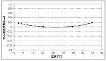
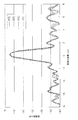
- the loss wavelength characteristic and temperature change of the arrayed waveguide analysis grating type optical multiplexer / demultiplexer 1 are shown in the graph of FIG.
- the horizontal axis indicates the relative deviation from the transmission center wavelength
- the vertical axis indicates the loss.
- the solid line shows the results at 20 ° C., the broken line at 50 ° C., the one-dot chain line at 70 ° C., and the two-dot chain line at ⁇ 5 ° C.
- the distortion of the spectrum is stable regardless of the temperature, and the low noise level is stable even when the temperature changes. Has been obtained. Therefore, crosstalk is small.
- the arrayed waveguide 28 is not fixed to the second glass plate 34 with an adhesive. This is because the influence on the arrayed waveguide 28 caused by the difference between the linear expansion coefficient of the second separation waveguide chip 16B and the linear expansion coefficient of the second glass plate 34 can be suppressed.
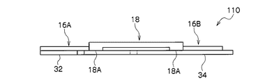
- Comparative Example 1 The same as in the first embodiment, except that the shape of the glass plate 34 is changed and the entire substrate 12B including the portion of the arrayed waveguide 28 is bonded and fixed to the second glass plate 34 in the second separation waveguide chip 16B.
- a plan view of an arrayed waveguide grating optical multiplexer / demultiplexer 110 according to Comparative Example 1 is shown in FIG. 15A, and a side view thereof is shown in FIG. 15B.
- a center wavelength variation of ⁇ 0.010 nm can be realized in a temperature range of ⁇ 5 to 70 ° C. I confirmed that there was no.
- the loss wavelength characteristic and temperature change of the arrayed waveguide analysis grating type optical multiplexer / demultiplexer 110 are shown in the graph of FIG.
- the horizontal axis indicates the relative deviation from the transmission center wavelength
- the vertical axis indicates the loss.
- the solid line shows the results at 20 ° C., the broken line at 50 ° C., the one-dot chain line at 70 ° C., and the two-dot chain line at ⁇ 5 ° C.
Abstract
Description
以下、本発明に係るアレイ導波路回折格子型光合分波器の一例について説明する。
また、導波路チップ16は、アレイ導波路の湾曲方向と同一の方向に同一の曲率で湾曲した平面形状とされている。したがって、外形が矩形状の導波路チップを有するアレイ導波路回折格子型光合分波器と比較してよりコンパクトに構成できる。
なお、接着面積が異なると、実効長が変わることがあり、温度特性にばらつきが生じる場合がある。

次に、アレイ導波路回折格子型光合分波器1の作用について説明する。
故に、パッケージサイズを、導波路チップの平面形状が矩形状であるアレイ導波路回折格子型光合分波器と同程度か、またはそれよりも小さくすることができる。
また、第1のガラス板32および第2のガラス板34の厚さ方向の寸法誤差の影響を受けることがない。
以下、本発明に係るアレイ導波路回折格子型光合分波器の別の例について説明する。
以下、本発明に係るアレイ導波路回折格子型光合分波器の更に別の例について説明する。
以下、本発明に係るアレイ導波路回折格子型光合分波器の更に別の例について説明する。
なお、第1の分離導波路チップ16Aの第1のガラス板32との貼り付け面は、補償部材18の長手方向の延長線と交わることが好ましい。このように、補償部材18の長手方向の延長線上を接着することで、温度履歴による中心波長シフトのヒステリシスが小さくなり、中心波長の温度依存性が安定する。
図10は補償部材18の長手方向の延長線上を接着している図1Aおよび図1Bに示すアレイ導波路回折格子型光合分波器に、20℃→50℃→70℃→50℃→20℃→-5℃→20℃の温度履歴を与えた場合の中心波長の変化を示す。図10から明らかなように、このような温度履歴を与えた場合においても20℃、50℃で中心波長は同一の値を示している。
実施形態1に記載のアレイ導波路回折格子型光合分波器1を作成し、このアレイ導波路回折格子型光合分波器1の温度特性について評価した。
ガラス板34の形状を変え、第2の分離導波路チップ16Bにおいて、アレイ導波路28の部分も含めて基板12B全体を第2のガラス板34に接着、固定した以外は、実施形態1と同様の構成を有するアレイ導波路回折格子型光合分波器110を作成し、温度特性について評価した。比較例1に係るアレイ導波路回折格子型光合分波器110の平面図を図15Aに、側面図を図15Bに示す。
Claims (4)
- 少なくとも1本の第1導波路と、前記第1導波路に接続された第1スラブ導波路と、前記第1スラブ導波路における前記第1導波路が接続された側とは反対側に一端が接続されているとともに、互いに異なる長さを有し、同一の方向に湾曲した複数のチャネル導波路からなるアレイ導波路と、前記アレイ導波路の他端に接続された第2スラブ導波路と、前記第2スラブ導波路における前記アレイ導波路が接続された側とは反対側に複数並設された状態で接続された第2導波路と、を有するアレイ導波路回折格子を備え、第1スラブ導波路および第2スラブ導波路の何れかにおいて第1の分離導波路チップと第2の分離導波路チップに分割されている導波路チップと、
前記第1の分離導波路チップを支持するための第1の基台と、
前記第2の分離導波路チップを支持するための第2の基台と、
温度変化に応じて伸縮することで前記第1および第2の分離導波路チップの相対位置をずらすことにより、前記導波路チップにおける前記アレイ導波路回折格子の光透過中心波長の温度依存性シフトを補償する補償部材と、
を備え、
前記第1の分離導波路チップは、前記アレイ導波路を含まない領域の少なくとも一部において、前記第1の基台に固定されており、
前記第2の分離導波路チップは、前記アレイ導波路を含まない領域の少なくとも一部において、前記第2の基台に固定されていることを特徴とするアレイ導波路回折格子型光合分波器。 - 前記第1および第2の基台における前記第1または第2の分離導波路チップの前記アレイ導波路を含む領域を支持する部分は切り欠かれていることを特徴とする請求項1に記載のアレイ導波路回折格子型光合分波器。
- 前記2つに分割された導波路チップの境界の部分は、クリップで厚さ方向に挟持されていることを特徴とする請求項1または2に記載のアレイ導波路回折格子型光合分波器。
- 前記第1および第2の基台には、前記クリップを位置決めするための開口部が形成されている請求項3に記載のアレイ導波路回折格子型光合分波器。
Priority Applications (3)
| Application Number | Priority Date | Filing Date | Title |
|---|---|---|---|
| JP2012522635A JPWO2012002368A1 (ja) | 2010-07-02 | 2011-06-28 | アレイ導波路回折格子型光合分波器 |
| CN2011800318470A CN102959440A (zh) | 2010-07-02 | 2011-06-28 | 阵列波导衍射光栅型光合波/分波器 |
| US13/361,285 US20120195552A1 (en) | 2010-07-02 | 2012-01-30 | Arrayed waveguide grating type optical multiplexer and demultiplexer |
Applications Claiming Priority (2)
| Application Number | Priority Date | Filing Date | Title |
|---|---|---|---|
| JP2010-152243 | 2010-07-02 | ||
| JP2010152243 | 2010-07-02 |
Related Child Applications (1)
| Application Number | Title | Priority Date | Filing Date |
|---|---|---|---|
| US13/361,285 Continuation US20120195552A1 (en) | 2010-07-02 | 2012-01-30 | Arrayed waveguide grating type optical multiplexer and demultiplexer |
Publications (1)
| Publication Number | Publication Date |
|---|---|
| WO2012002368A1 true WO2012002368A1 (ja) | 2012-01-05 |
Family
ID=45402075
Family Applications (1)
| Application Number | Title | Priority Date | Filing Date |
|---|---|---|---|
| PCT/JP2011/064769 WO2012002368A1 (ja) | 2010-07-02 | 2011-06-28 | アレイ導波路回折格子型光合分波器 |
Country Status (4)
| Country | Link |
|---|---|
| US (1) | US20120195552A1 (ja) |
| JP (1) | JPWO2012002368A1 (ja) |
| CN (1) | CN102959440A (ja) |
| WO (1) | WO2012002368A1 (ja) |
Families Citing this family (4)
| Publication number | Priority date | Publication date | Assignee | Title |
|---|---|---|---|---|
| CN103018825B (zh) * | 2013-01-11 | 2014-06-18 | 武汉光迅科技股份有限公司 | 一种实现分段温度补偿的无热阵列波导光栅 |
| EP3077860A4 (en) * | 2013-12-03 | 2017-08-02 | Intel Corporation | Monolithic physically displaceable optical waveguides |
| CN104765103B (zh) * | 2015-04-29 | 2018-01-19 | 武汉光迅科技股份有限公司 | 一种降低阵列波导光栅非线性温度效应的装置 |
| CN110515155A (zh) * | 2019-08-29 | 2019-11-29 | 易锐光电科技(安徽)有限公司 | 一种波长可控阵列波导光栅 |
Citations (10)
| Publication number | Priority date | Publication date | Assignee | Title |
|---|---|---|---|---|
| JPH10160960A (ja) * | 1996-12-04 | 1998-06-19 | Hitachi Cable Ltd | 光モジュール |
| JP2002071994A (ja) * | 1999-12-27 | 2002-03-12 | Furukawa Electric Co Ltd:The | アレイ導波路回折格子型光合分波器およびその製造方法 |
| JP2002341163A (ja) * | 2001-03-13 | 2002-11-27 | Furukawa Electric Co Ltd:The | アレイ導波路回折格子型光合分波器 |
| JP2003066254A (ja) * | 2001-08-27 | 2003-03-05 | Furukawa Electric Co Ltd:The | アレイ導波路回折格子型光合分波器およびその製造方法 |
| JP2003227945A (ja) * | 2002-02-01 | 2003-08-15 | Sumitomo Electric Ind Ltd | 光モジュール |
| JP2004020737A (ja) * | 2002-06-13 | 2004-01-22 | Furukawa Electric Co Ltd:The | アレイ導波路回折格子およびその製造方法 |
| JP2007536567A (ja) * | 2004-05-05 | 2007-12-13 | ライトウェイブ マイクロシステムズ コーポレーション | アサーマルawgおよび可変幅の溝を用いる低消費電力awg |
| JP2008538820A (ja) * | 2005-01-07 | 2008-11-06 | ポインテク インコーポレイション | 温度無依存性アレイ導波路回折格子及び製作方法 |
| JP2010032939A (ja) * | 2008-07-31 | 2010-02-12 | Furukawa Electric Co Ltd:The | アレイ導波路回折格子の位置合わせ装置 |
| JP2011034056A (ja) * | 2009-07-08 | 2011-02-17 | Furukawa Electric Co Ltd:The | アレイ導波路回折格子型光合分波器 |
Family Cites Families (7)
| Publication number | Priority date | Publication date | Assignee | Title |
|---|---|---|---|---|
| US5905824A (en) * | 1997-12-09 | 1999-05-18 | Delisle; Vincent | Temperature compensated insensitive optical multiplexor/demultiplexor |
| JP4494599B2 (ja) * | 2000-07-14 | 2010-06-30 | 古河電気工業株式会社 | アレイ導波路回折格子型光合分波器 |
| JP3630085B2 (ja) * | 2000-09-14 | 2005-03-16 | 日本電気株式会社 | アレイ導波路回折格子素子の製造方法およびアレイ導波路回折格子素子 |
| JPWO2002033462A1 (ja) * | 2000-10-13 | 2004-02-26 | 古河電気工業株式会社 | アレイ導波路型回折格子およびその光透過中心波長補正方法 |
| US6738545B1 (en) * | 2002-03-18 | 2004-05-18 | Lightwave Microsystems Corporation | Athermal AWG and AWG with low power consumption using groove of changeable width |
| JP2007065562A (ja) * | 2005-09-02 | 2007-03-15 | Furukawa Electric Co Ltd:The | アレイ導波路回折格子 |
| US7447394B2 (en) * | 2006-09-29 | 2008-11-04 | Neophotonics Corporation | Stable center wavelength performance in non-rectilinearly shaped optical integrated circuit chip |
-
2011
- 2011-06-28 JP JP2012522635A patent/JPWO2012002368A1/ja not_active Withdrawn
- 2011-06-28 CN CN2011800318470A patent/CN102959440A/zh active Pending
- 2011-06-28 WO PCT/JP2011/064769 patent/WO2012002368A1/ja active Application Filing
-
2012
- 2012-01-30 US US13/361,285 patent/US20120195552A1/en not_active Abandoned
Patent Citations (10)
| Publication number | Priority date | Publication date | Assignee | Title |
|---|---|---|---|---|
| JPH10160960A (ja) * | 1996-12-04 | 1998-06-19 | Hitachi Cable Ltd | 光モジュール |
| JP2002071994A (ja) * | 1999-12-27 | 2002-03-12 | Furukawa Electric Co Ltd:The | アレイ導波路回折格子型光合分波器およびその製造方法 |
| JP2002341163A (ja) * | 2001-03-13 | 2002-11-27 | Furukawa Electric Co Ltd:The | アレイ導波路回折格子型光合分波器 |
| JP2003066254A (ja) * | 2001-08-27 | 2003-03-05 | Furukawa Electric Co Ltd:The | アレイ導波路回折格子型光合分波器およびその製造方法 |
| JP2003227945A (ja) * | 2002-02-01 | 2003-08-15 | Sumitomo Electric Ind Ltd | 光モジュール |
| JP2004020737A (ja) * | 2002-06-13 | 2004-01-22 | Furukawa Electric Co Ltd:The | アレイ導波路回折格子およびその製造方法 |
| JP2007536567A (ja) * | 2004-05-05 | 2007-12-13 | ライトウェイブ マイクロシステムズ コーポレーション | アサーマルawgおよび可変幅の溝を用いる低消費電力awg |
| JP2008538820A (ja) * | 2005-01-07 | 2008-11-06 | ポインテク インコーポレイション | 温度無依存性アレイ導波路回折格子及び製作方法 |
| JP2010032939A (ja) * | 2008-07-31 | 2010-02-12 | Furukawa Electric Co Ltd:The | アレイ導波路回折格子の位置合わせ装置 |
| JP2011034056A (ja) * | 2009-07-08 | 2011-02-17 | Furukawa Electric Co Ltd:The | アレイ導波路回折格子型光合分波器 |
Also Published As
| Publication number | Publication date |
|---|---|
| US20120195552A1 (en) | 2012-08-02 |
| JPWO2012002368A1 (ja) | 2013-08-29 |
| CN102959440A (zh) | 2013-03-06 |
Similar Documents
| Publication | Publication Date | Title |
|---|---|---|
| WO2012002250A1 (ja) | アレイ導波路回折格子型光合分波器 | |
| US8457459B2 (en) | Arrayed-waveguide-grating-type optical multiplexer/demultiplexer | |
| US6563986B2 (en) | Arrayed waveguide grating | |
| KR100360766B1 (ko) | 배열된 도파관격자형 광학멀티플레서/디멀티플렉서 및 그제조방법 | |
| KR20080045256A (ko) | 어레이 도파로 회절 격자 | |
| JP3448551B2 (ja) | アレイ導波路型回折格子 | |
| JP5351522B2 (ja) | 光特性補償のための温度無依存のアレイ導波路回折格子合分波器及びその製作方法 | |
| US6668116B2 (en) | Arrayed waveguide grating type optical multiplexer/demultiplexer | |
| JP4667927B2 (ja) | アレイ導波路回折格子型光合分波器 | |
| JP5027031B2 (ja) | アレイ導波路回折格子型光合分波器 | |
| WO2012002368A1 (ja) | アレイ導波路回折格子型光合分波器 | |
| US6668117B2 (en) | Arrayed waveguide grating optical multiplexer demultiplexer | |
| US6735364B2 (en) | Arrayed waveguide grating optical multiplexer/demultiplexer and method for manufacturing the same | |
| US20130142483A1 (en) | Arrayed waveguide grating multiplexer-demultiplexer | |
| JP2000131540A (ja) | 光合分波器 | |
| WO2014024557A1 (ja) | アレイ導波路回折格子型光合分波器 | |
| JP5075048B2 (ja) | アレイ導波路回折格子の位置合わせ方法およびアレイ導波路回折格子の位置合わせ装置 | |
| JP4762422B2 (ja) | アレイ導波路型回折格子 | |
| JP2003066254A (ja) | アレイ導波路回折格子型光合分波器およびその製造方法 | |
| JP2010204696A (ja) | アレイ導波路回折格子の作製方法 | |
| JP2007094063A (ja) | 光波長合分波器 | |
| JP2001330739A (ja) | アレイ導波路型回折格子 | |
| JP2001215348A (ja) | アレイ導波路型回折格子 | |
| JP2010097231A (ja) | アレイ導波路回折格子型光合分波器 |
Legal Events
| Date | Code | Title | Description |
|---|---|---|---|
| WWE | Wipo information: entry into national phase |
Ref document number: 201180031847.0 Country of ref document: CN |
|
| 121 | Ep: the epo has been informed by wipo that ep was designated in this application |
Ref document number: 11800832 Country of ref document: EP Kind code of ref document: A1 |
|
| WWE | Wipo information: entry into national phase |
Ref document number: 2012522635 Country of ref document: JP |
|
| NENP | Non-entry into the national phase |
Ref country code: DE |
|
| 122 | Ep: pct application non-entry in european phase |
Ref document number: 11800832 Country of ref document: EP Kind code of ref document: A1 |