WO2011158528A1 - 炭化珪素半導体装置の製造方法および炭化珪素半導体装置の製造装置 - Google Patents
炭化珪素半導体装置の製造方法および炭化珪素半導体装置の製造装置 Download PDFInfo
- Publication number
- WO2011158528A1 WO2011158528A1 PCT/JP2011/054010 JP2011054010W WO2011158528A1 WO 2011158528 A1 WO2011158528 A1 WO 2011158528A1 JP 2011054010 W JP2011054010 W JP 2011054010W WO 2011158528 A1 WO2011158528 A1 WO 2011158528A1
- Authority
- WO
- WIPO (PCT)
- Prior art keywords
- semiconductor device
- forming
- oxide film
- silicon carbide
- sic semiconductor
- Prior art date
Links
Images

Classifications
-
- H—ELECTRICITY
- H01—ELECTRIC ELEMENTS
- H01L—SEMICONDUCTOR DEVICES NOT COVERED BY CLASS H10
- H01L21/00—Processes or apparatus adapted for the manufacture or treatment of semiconductor or solid state devices or of parts thereof
- H01L21/02—Manufacture or treatment of semiconductor devices or of parts thereof
- H01L21/02104—Forming layers
- H01L21/02107—Forming insulating materials on a substrate
- H01L21/02109—Forming insulating materials on a substrate characterised by the type of layer, e.g. type of material, porous/non-porous, pre-cursors, mixtures or laminates
- H01L21/02112—Forming insulating materials on a substrate characterised by the type of layer, e.g. type of material, porous/non-porous, pre-cursors, mixtures or laminates characterised by the material of the layer
- H01L21/02123—Forming insulating materials on a substrate characterised by the type of layer, e.g. type of material, porous/non-porous, pre-cursors, mixtures or laminates characterised by the material of the layer the material containing silicon
- H01L21/02167—Forming insulating materials on a substrate characterised by the type of layer, e.g. type of material, porous/non-porous, pre-cursors, mixtures or laminates characterised by the material of the layer the material containing silicon the material being a silicon carbide not containing oxygen, e.g. SiC, SiC:H or silicon carbonitrides
-
- H—ELECTRICITY
- H01—ELECTRIC ELEMENTS
- H01L—SEMICONDUCTOR DEVICES NOT COVERED BY CLASS H10
- H01L21/00—Processes or apparatus adapted for the manufacture or treatment of semiconductor or solid state devices or of parts thereof
- H01L21/02—Manufacture or treatment of semiconductor devices or of parts thereof
- H01L21/02041—Cleaning
- H01L21/02057—Cleaning during device manufacture
-
- H—ELECTRICITY
- H01—ELECTRIC ELEMENTS
- H01L—SEMICONDUCTOR DEVICES NOT COVERED BY CLASS H10
- H01L21/00—Processes or apparatus adapted for the manufacture or treatment of semiconductor or solid state devices or of parts thereof
- H01L21/02—Manufacture or treatment of semiconductor devices or of parts thereof
- H01L21/02104—Forming layers
- H01L21/02107—Forming insulating materials on a substrate
- H01L21/02225—Forming insulating materials on a substrate characterised by the process for the formation of the insulating layer
- H01L21/02227—Forming insulating materials on a substrate characterised by the process for the formation of the insulating layer formation by a process other than a deposition process
- H01L21/0223—Forming insulating materials on a substrate characterised by the process for the formation of the insulating layer formation by a process other than a deposition process formation by oxidation, e.g. oxidation of the substrate
- H01L21/02233—Forming insulating materials on a substrate characterised by the process for the formation of the insulating layer formation by a process other than a deposition process formation by oxidation, e.g. oxidation of the substrate of the semiconductor substrate or a semiconductor layer
- H01L21/02236—Forming insulating materials on a substrate characterised by the process for the formation of the insulating layer formation by a process other than a deposition process formation by oxidation, e.g. oxidation of the substrate of the semiconductor substrate or a semiconductor layer group IV semiconductor
-
- H—ELECTRICITY
- H01—ELECTRIC ELEMENTS
- H01L—SEMICONDUCTOR DEVICES NOT COVERED BY CLASS H10
- H01L21/00—Processes or apparatus adapted for the manufacture or treatment of semiconductor or solid state devices or of parts thereof
- H01L21/02—Manufacture or treatment of semiconductor devices or of parts thereof
- H01L21/02104—Forming layers
- H01L21/02107—Forming insulating materials on a substrate
- H01L21/02296—Forming insulating materials on a substrate characterised by the treatment performed before or after the formation of the layer
- H01L21/02299—Forming insulating materials on a substrate characterised by the treatment performed before or after the formation of the layer pre-treatment
- H01L21/02301—Forming insulating materials on a substrate characterised by the treatment performed before or after the formation of the layer pre-treatment in-situ cleaning
-
- H—ELECTRICITY
- H01—ELECTRIC ELEMENTS
- H01L—SEMICONDUCTOR DEVICES NOT COVERED BY CLASS H10
- H01L21/00—Processes or apparatus adapted for the manufacture or treatment of semiconductor or solid state devices or of parts thereof
- H01L21/02—Manufacture or treatment of semiconductor devices or of parts thereof
- H01L21/04—Manufacture or treatment of semiconductor devices or of parts thereof the devices having potential barriers, e.g. a PN junction, depletion layer or carrier concentration layer
- H01L21/0445—Manufacture or treatment of semiconductor devices or of parts thereof the devices having potential barriers, e.g. a PN junction, depletion layer or carrier concentration layer the devices having semiconductor bodies comprising crystalline silicon carbide
- H01L21/0455—Making n or p doped regions or layers, e.g. using diffusion
- H01L21/046—Making n or p doped regions or layers, e.g. using diffusion using ion implantation
-
- H—ELECTRICITY
- H01—ELECTRIC ELEMENTS
- H01L—SEMICONDUCTOR DEVICES NOT COVERED BY CLASS H10
- H01L21/00—Processes or apparatus adapted for the manufacture or treatment of semiconductor or solid state devices or of parts thereof
- H01L21/02—Manufacture or treatment of semiconductor devices or of parts thereof
- H01L21/04—Manufacture or treatment of semiconductor devices or of parts thereof the devices having potential barriers, e.g. a PN junction, depletion layer or carrier concentration layer
- H01L21/0445—Manufacture or treatment of semiconductor devices or of parts thereof the devices having potential barriers, e.g. a PN junction, depletion layer or carrier concentration layer the devices having semiconductor bodies comprising crystalline silicon carbide
- H01L21/048—Making electrodes
- H01L21/049—Conductor-insulator-semiconductor electrodes, e.g. MIS contacts
-
- H—ELECTRICITY
- H01—ELECTRIC ELEMENTS
- H01L—SEMICONDUCTOR DEVICES NOT COVERED BY CLASS H10
- H01L21/00—Processes or apparatus adapted for the manufacture or treatment of semiconductor or solid state devices or of parts thereof
- H01L21/02—Manufacture or treatment of semiconductor devices or of parts thereof
- H01L21/04—Manufacture or treatment of semiconductor devices or of parts thereof the devices having potential barriers, e.g. a PN junction, depletion layer or carrier concentration layer
- H01L21/18—Manufacture or treatment of semiconductor devices or of parts thereof the devices having potential barriers, e.g. a PN junction, depletion layer or carrier concentration layer the devices having semiconductor bodies comprising elements of Group IV of the Periodic Table or AIIIBV compounds with or without impurities, e.g. doping materials
- H01L21/30—Treatment of semiconductor bodies using processes or apparatus not provided for in groups H01L21/20 - H01L21/26
- H01L21/302—Treatment of semiconductor bodies using processes or apparatus not provided for in groups H01L21/20 - H01L21/26 to change their surface-physical characteristics or shape, e.g. etching, polishing, cutting
- H01L21/306—Chemical or electrical treatment, e.g. electrolytic etching
- H01L21/3065—Plasma etching; Reactive-ion etching
-
- H—ELECTRICITY
- H10—SEMICONDUCTOR DEVICES; ELECTRIC SOLID-STATE DEVICES NOT OTHERWISE PROVIDED FOR
- H10D—INORGANIC ELECTRIC SEMICONDUCTOR DEVICES
- H10D12/00—Bipolar devices controlled by the field effect, e.g. insulated-gate bipolar transistors [IGBT]
- H10D12/01—Manufacture or treatment
- H10D12/031—Manufacture or treatment of IGBTs
-
- H—ELECTRICITY
- H10—SEMICONDUCTOR DEVICES; ELECTRIC SOLID-STATE DEVICES NOT OTHERWISE PROVIDED FOR
- H10D—INORGANIC ELECTRIC SEMICONDUCTOR DEVICES
- H10D30/00—Field-effect transistors [FET]
- H10D30/01—Manufacture or treatment
- H10D30/021—Manufacture or treatment of FETs having insulated gates [IGFET]
- H10D30/028—Manufacture or treatment of FETs having insulated gates [IGFET] of double-diffused metal oxide semiconductor [DMOS] FETs
- H10D30/0291—Manufacture or treatment of FETs having insulated gates [IGFET] of double-diffused metal oxide semiconductor [DMOS] FETs of vertical DMOS [VDMOS] FETs
-
- H—ELECTRICITY
- H10—SEMICONDUCTOR DEVICES; ELECTRIC SOLID-STATE DEVICES NOT OTHERWISE PROVIDED FOR
- H10D—INORGANIC ELECTRIC SEMICONDUCTOR DEVICES
- H10D30/00—Field-effect transistors [FET]
- H10D30/60—Insulated-gate field-effect transistors [IGFET]
- H10D30/64—Double-diffused metal-oxide semiconductor [DMOS] FETs
- H10D30/66—Vertical DMOS [VDMOS] FETs
-
- H—ELECTRICITY
- H10—SEMICONDUCTOR DEVICES; ELECTRIC SOLID-STATE DEVICES NOT OTHERWISE PROVIDED FOR
- H10D—INORGANIC ELECTRIC SEMICONDUCTOR DEVICES
- H10D62/00—Semiconductor bodies, or regions thereof, of devices having potential barriers
- H10D62/80—Semiconductor bodies, or regions thereof, of devices having potential barriers characterised by the materials
- H10D62/83—Semiconductor bodies, or regions thereof, of devices having potential barriers characterised by the materials being Group IV materials, e.g. B-doped Si or undoped Ge
- H10D62/832—Semiconductor bodies, or regions thereof, of devices having potential barriers characterised by the materials being Group IV materials, e.g. B-doped Si or undoped Ge being Group IV materials comprising two or more elements, e.g. SiGe
- H10D62/8325—Silicon carbide
Definitions
- the present invention relates to a method for manufacturing a silicon carbide (SiC) semiconductor device and an apparatus for manufacturing an SiC semiconductor device, and more particularly to a method for manufacturing an SiC semiconductor device having an oxide film and a manufacturing apparatus used in the manufacturing method.
- SiC silicon carbide
- Si silicon
- MOSFETs Metal Oxide Semiconductor Field Effect Transistors
- an epitaxial layer is formed on a silicon (Si) substrate to produce a Si semiconductor.
- an ion implantation step is performed for the purpose of introducing an impurity (dopant) into the Si semiconductor, and then the Si semiconductor is subjected to heat treatment (activation annealing treatment) for the purpose of activating the introduced impurity.
- heat treatment activation annealing treatment
- a gate oxide film is formed on the surface of the Si semiconductor after the heat treatment, and an electrode is formed thereon.
- cleaning is performed to remove deposits such as particles and impurities such as particles adhering to the surface of the Si substrate.
- a cleaning method using a chemical solution such as RCA cleaning is widely adopted.
- an Si oxide film is formed on the surface of the Si substrate by cleaning the surface of the Si substrate with a chemical solution containing sulfuric acid and hydrogen peroxide. Particles and metal impurities are taken into the inside and the surface of the Si oxide film.
- the Si substrate is washed with a dilute hydrofluoric acid aqueous solution to remove the Si oxide film by etching and remove particles and metal impurities.
- Patent Document 1 Japanese Patent Laid-Open No. 6-314679 (Patent Document 1) and Japanese Patent Laid-Open No. 4-354334 (Patent Document 2) oxidize the surface of a Si substrate using ozone water. Thereafter, a method has been developed for removing particles and metal impurities on the Si substrate by removing the oxide film.
- SiC has a large band gap, and a maximum dielectric breakdown electric field and thermal conductivity are larger than those of Si, while carrier mobility is as large as that of Si, and an electron saturation drift velocity and withstand voltage are also large. Therefore, application to a semiconductor device that is required to have high efficiency, high breakdown voltage, and large capacity is expected. Therefore, the present inventor has paid attention to the use of a SiC semiconductor for a semiconductor device. Then, the present inventor has conceived to clean the surface for forming an oxide film constituting the SiC semiconductor device in the SiC semiconductor in order to manufacture a higher quality SiC semiconductor device.
- the present inventor has revealed for the first time that the surface of the SiC semiconductor is difficult to be oxidized because SiC is a thermally stable compound than Si. That is, the above cleaning method can oxidize the surface of Si, but cannot sufficiently oxidize the surface of SiC. For this reason, particles and impurities cannot be removed from the SiC surface, and the SiC surface cannot be sufficiently cleaned. If the surface of the SiC semiconductor is not cleaned, an oxide film cannot be formed on the cleaned SiC semiconductor. As a result, the quality of the manufactured SiC semiconductor device is degraded.
- an object of the present invention is to provide a method for manufacturing a high-quality SiC semiconductor device and a manufacturing apparatus used in this method.
- the present invention is a method of manufacturing an SiC semiconductor device, the step of preparing an SiC semiconductor including a first surface in which an impurity (dopant) is implanted at least in part, and the first surface of the SiC semiconductor. And a step of forming a second surface by dry etching using a gas containing hydrogen gas, and a step of forming an oxide film constituting the SiC semiconductor device on the second surface.
- a method for manufacturing a semiconductor device is a method of manufacturing an SiC semiconductor device, the step of preparing an SiC semiconductor including a first surface in which an impurity (dopant) is implanted at least in part, and the first surface of the SiC semiconductor.
- a step of forming a second surface by dry etching using a gas containing hydrogen gas, and a step of forming an oxide film constituting the SiC semiconductor device on the second surface.
- the first surface in which impurities are implanted into at least a part of the SiC semiconductor is also dry-etched using a gas containing hydrogen gas (hereinafter also referred to as “hydrogen etching”). )
- a gas containing hydrogen gas hereinafter also referred to as “hydrogen etching”.
- hydrogen etching a gas containing hydrogen gas
- a high quality SiC semiconductor device can be manufactured by forming an oxide film constituting the SiC semiconductor device on the cleaned second surface.
- the SiC semiconductor is a stable compound, even if hydrogen etching is performed, the SiC semiconductor is less damaged. Therefore, the SiC semiconductor can be cleaned so that the surface characteristics are good. Therefore, a high quality SiC semiconductor device can be manufactured.
- a step of forming an oxide film is performed without cleaning using a liquid phase.
- hydrogen etching is performed in a temperature range of 1300 ° C. to 1650 ° C.
- the etching rate can be increased, and by performing the etching at a temperature of 1650 ° C. or lower, it is possible to suppress the etching rate from becoming too high, and thus can be easily controlled. That is, by performing the hydrogen etching within the above temperature range, it is possible to control the etching rate to be suitable, so that the first surface can be etched with high accuracy, and the quality of the SiC semiconductor device can be further improved. .
- the step of forming the oxide film includes forming a film containing silicon (Si) on the second surface, and oxidizing the film containing Si to form the oxide film. Form.
- the present inventor found that the second surface in which the impurity (dopant) is implanted into at least a part of the SiC semiconductor has different impurity (dopant) concentration and the type of the impurity (dopant), so that the oxidation rate in the depth direction varies.
- the invention was completed. Since the film containing Si is formed on the second surface, the influence of the second surface state can be reduced on the quality of the film containing Si. For this reason, the quality of the film containing Si can be made uniform. Therefore, the quality of the SiC semiconductor device can be further improved.
- the gas in the method of manufacturing the SiC semiconductor device, in the step of forming the second surface, the gas further includes hydrogen chloride gas.
- the etching rate of the SiC semiconductor can be increased by using hydrogen chloride gas together with hydrogen gas. Therefore, the manufacturing tact of the SiC semiconductor device can be shortened.
- the gas in the method for manufacturing the SiC semiconductor device, in the step of forming the second surface, the gas further includes a hydrocarbon gas.
- the surface morphology of the SiC semiconductor can be improved by using a hydrocarbon gas together with the hydrogen gas. Therefore, the quality of the SiC semiconductor device can be further improved.
- the SiC semiconductor is disposed in an atmosphere in which air is blocked between the step of forming the second surface and the step of forming the oxide film.
- the SiC semiconductor on which the clean second surface is formed can be subjected to the step of forming an oxide film constituting the SiC semiconductor device in the next step without being exposed to the atmosphere. For this reason, it can prevent that the surface of the cleaned SiC semiconductor is polluted by air
- the present invention also provides a removal portion for removing, by dry etching using a gas containing hydrogen gas, a first surface in which an impurity (dopant) is implanted at least in part in the SiC semiconductor, A connecting portion for forming an oxide film constituting the SiC semiconductor device on the second surface formed by removing the surface of 1 and connecting the removing portion and the forming portion so that the SiC semiconductor can be transported
- the region where the SiC semiconductor is transported in the connecting portion is a SiC semiconductor device manufacturing apparatus capable of blocking the atmosphere.
- the first surface in which impurities are implanted into at least a part can be hydrogen etched by the removing portion.
- the SiC semiconductor after hydrogen etching by the removal part can be conveyed to a formation part via the connection part of the atmosphere cut off from air
- an oxide film constituting the SiC semiconductor device can be formed on the second surface in the formation portion. That is, a series of processes from the process of cleaning the SiC semiconductor by hydrogen etching to the process of forming the oxide film can be performed in a state where the process is cut off from the atmosphere. Therefore, according to this manufacturing apparatus, a high-quality SiC semiconductor device can be manufactured.
- a high-quality SiC semiconductor device is manufactured by using the cleaning method of the SiC semiconductor that can express the cleaning of the SiC semiconductor. can do.
- FIG. 1 is a cross-sectional view schematically showing an epitaxial wafer used in Example 1, Comparative Example 1 and Comparative Example 2.
- FIG. It is a spectrum which shows the result of having measured the surface of the SiC semiconductor of the comparative example 1 by TXRF. It is a spectrum which shows the result of having measured the surface of the SiC semiconductor of the comparative example 2 by TXRF.
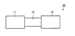
- FIG. 1 is a schematic diagram of an apparatus for manufacturing an SiC semiconductor device according to Embodiment 1 of the present invention. With reference to FIG. 1, a SiC semiconductor device manufacturing apparatus according to an embodiment of the present invention will be described.
- the SiC semiconductor device manufacturing apparatus 10 includes a removing unit 11, a forming unit 12, and a connecting unit 13.
- the removal unit 11 and the formation unit 12 are connected by a connection unit 13.
- the insides of the removing unit 11, the forming unit 12, and the connecting unit 13 are shielded from the atmosphere, and the insides can communicate with each other.
- the removal unit 11 forms a second surface by performing hydrogen etching on the first surface in which impurities are implanted into at least a part of the SiC semiconductor.
- a hydrogen etching apparatus is used for the removing unit 11.
- the hydrogen etching apparatus used in the removing unit 11 is not particularly limited, and for example, a high-frequency heating furnace can be used.
- the forming unit 12 forms an oxide film constituting the SiC semiconductor device on the second surface.
- An oxide film forming apparatus is used for the forming unit 12.
- the oxide film forming apparatus used in the forming unit 12 is not particularly limited.
- the dry oxidation (thermal oxidation) apparatus, the sputtering apparatus, the CVD (Chemical Vapor Deposition) apparatus, and heating in an oxygen atmosphere containing water vapor are performed.
- a wet oxidation device or a pyrogenic oxidation device can be used, and a dry oxidation device is preferably used.
- the connecting unit 13 connects the removing unit 11 and the forming unit 12 so that the SiC semiconductor can be transported.
- the region (internal space) where the epitaxial wafer is transported in the connecting portion 13 can be shut off from the atmosphere.
- the interruption of the atmosphere means an atmosphere in which no atmosphere is mixed, for example, an atmosphere made of at least one kind of gas such as nitrogen gas, hydrogen gas and inert gas, or a vacuum.
- the atmosphere from which the air is blocked is, for example, nitrogen (N), hydrogen (H), helium (He), neon (Ne), argon (Ar), krypton (Kr), xenon (Xe), radon ( Rn), or an atmosphere filled with a gas composed of a combination of these, or a vacuum.
- connection part 13 makes the inside of the removal part 11 and the inside of the formation part 12 communicate.
- Connection unit 13 has a space for transporting the SiC semiconductor unloaded from removal unit 11 to formation unit 12. That is, the connection part 13 is installed in order to convey from the removal part 11 to the formation part 12 so that a SiC semiconductor may not be open
- the connecting portion 13 has such a size that the SiC semiconductor can be transported inside. Moreover, the connection part 13 may have a magnitude
- the connecting portion 13 is a load lock chamber that connects, for example, the outlet of the removing portion 11 and the inlet of the forming portion 12.
- the manufacturing apparatus 10 may further include a first transport unit that is disposed inside the connection unit 13 and transports the SiC semiconductor from the removal unit 11 to the formation unit 12.
- the manufacturing apparatus 10 takes out the SiC semiconductor in which the gate oxide film 126 is formed in the forming unit 12 to the outside of the manufacturing apparatus 10 or transports the SiC semiconductor to the electrode forming unit for forming the electrode in an atmosphere in which the atmosphere is shut off. You may further provide the conveyance part.
- the first transport unit and the second transport unit may be the same or different.
- the manufacturing apparatus 10 may further include a blocking unit that is disposed between the removing unit 11 and the connecting unit 13 and that blocks the inside of the removing unit 11 and the inside of the connecting unit 13.
- the manufacturing apparatus 10 may further include a blocking unit that is disposed between the forming unit 12 and the connecting unit 13 and that blocks the inside of the forming unit 12 and the inside of the connecting unit 13.
- the blocking unit for example, a valve or a door that can block each communication unit can be used.
- the manufacturing apparatus 10 may further include a vacuum pump for discharging the internal atmospheric gas and a replacement gas cylinder for replacing the internal atmospheric gas.
- the vacuum pump and the replacement gas cylinder may be connected to each of the removing unit 11, the forming unit 12, and the connecting unit 13, or may be connected to at least one of them.
- the manufacturing apparatus 10 may include various elements other than those described above, for example, an electrode forming portion for forming an electrode on the oxide film, but the illustration and description of these elements are omitted for convenience of description. .
- connection part 13 for example, a chamber in which the atmosphere is shut off may be used, and the removal part 11 and the formation part 12 may be arranged in this chamber.
- FIG. 2 is a flowchart showing a method of manufacturing the SiC semiconductor device in the first embodiment of the present invention.
- 3 to 6 are diagrams showing the configuration of the SiC semiconductor formed in each step of the method of manufacturing the SiC semiconductor device according to the first embodiment of the present invention.
- FIG. 3 is a cross-sectional view schematically showing a SiC semiconductor to be prepared
- FIG. 4 is a diagram for explaining a manufacturing process of the SiC semiconductor to be prepared.
- FIG. 5 is a cross-sectional view schematically showing a SiC semiconductor in which an oxide film is formed
- FIG. 6 is a cross-sectional view schematically showing a SiC semiconductor in which a source contact electrode and a drain electrode are formed.
- FIG. 7 is a cross sectional view schematically showing the SiC semiconductor device manufactured in the first embodiment of the present invention.
- a method of manufacturing SiC semiconductor device 200 shown in FIG. 7 as an SiC semiconductor will be described.
- SiC semiconductor device manufacturing apparatus 10 shown in FIG. 1 is used.
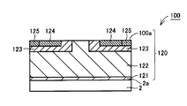
- an epitaxial wafer 100 is prepared as an SiC semiconductor including the first surface 100a in which impurities are implanted at least partially (step S1).
- an epitaxial wafer 100 is prepared as an SiC semiconductor in which an epitaxial layer 120 having a region into which impurities are implanted is formed on the surface 2 a of the SiC substrate 2.
- the SiC substrate 2 is not particularly limited, but can be prepared, for example, by the following method.
- a SiC ingot grown by a vapor phase growth method such as a sublimation method or a CVD method, a liquid phase growth method, or the like is prepared. Thereafter, a SiC substrate having a surface is cut out from the SiC ingot.
- the cutting method is not particularly limited, and the SiC substrate is cut from the SiC ingot by slicing or the like.
- the surface of the cut SiC substrate is polished.
- the surface to be polished may be only the front surface, or the back surface opposite to the front surface may be further polished.
- the polishing method is not particularly limited, but for example, CMP (Chemical Mechanical Polishing) is performed to flatten the surface and reduce damage such as scratches.
- CMP Chemical Mechanical Polishing
- colloidal silica is used as an abrasive, and an adhesive, wax, or the like is used as a fixing agent.
- other polishing such as an electric field polishing method, a chemical polishing method, and a mechanical polishing method may be further performed. Polishing may be omitted.
- SiC substrate 2 having surface 2a can be prepared.
- SiC substrate 2 for example, a substrate having an n-type conductivity and a resistance of 0.02 ⁇ cm is used.
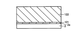
- the epitaxial layer 120 on the SiC substrate 2 can be formed by, for example, the following method.
- buffer layer 121 is formed on surface 2 a of SiC substrate 2.
- Buffer layer 121 is an epitaxial layer made of, for example, n-type SiC and having a thickness of 0.5 ⁇ m, for example.
- the concentration of the n-type conductive impurity in the buffer layer 121 is, for example, 5 ⁇ 10 17 cm ⁇ 3 .
- the drift layer 122 is formed on the buffer layer 121.
- drift layer 122 a layer made of SiC of n-type conductivity is formed by vapor phase growth, liquid phase growth, or the like.
- the thickness of drift layer 122 is, for example, 10 ⁇ m.
- the concentration of the n-type conductive impurity in drift layer 122 is, for example, 5 ⁇ 10 15 cm ⁇ 3 .
- p body region 123, n source region 124, and p + region 125 are formed as follows. First, a body region 123 is formed by selectively injecting a p-type impurity into part of the drift layer 122. Thereafter, a source region 124 is formed by selectively injecting n-type conductive impurities into a predetermined region, and p-type by selectively injecting p-type conductive impurities with a p-type conductivity into the predetermined region. A + region 125 is formed. The selective implantation of conductive impurities is performed using a mask made of an oxide film, for example.
- each implantation profile takes into account the thickness removed by hydrogen etching in step S2 described later. That is, when the first surface 100a of the epitaxial layer is removed in the hydrogen etching step S2, the impurity diffusion region including the p body region 123, the n source region 124, and the p + region 125 is arranged in a desired arrangement. Control the ion implantation.
- activation annealing treatment may be performed.
- annealing is performed in an argon atmosphere at a heating temperature of 1700 ° C. for 30 minutes.
- the epitaxial wafer 100 including the SiC substrate 2 and the epitaxial layer 120 formed on the SiC substrate 2 can be prepared.
- the second surface 100b (see FIG. 5) is formed by hydrogen etching the first surface 100a of the prepared epitaxial wafer 100 (step S2).
- the first surface 100a is removed by the removing unit 11 of the manufacturing apparatus 10 shown in FIG.
- the first surface 100a of the epitaxial layer 120 is subjected to hydrogen etching, whereby impurities, particles, and the like attached to the first surface 100a can be removed together with the first surface 100a.
- a clean second surface 100b is formed by removing impurities, particles, and the like (see FIG. 5).
- the etching depth (the etching amount in the direction from the first surface 100a toward the SiC substrate 2) is preferably 0.1 ⁇ m or more and more preferably 0.5 ⁇ m or more because of the etching amount that is easily controlled. preferable.
- the etching depth is preferably not less than 1 molecular layer and not more than 10 nm.
- the surface region of the Si semiconductor may be damaged due to the above-described implantation step, impurities, particles, and the like are removed and the rough surface is removed by, for example, making the etching depth greater than 10 nm and less than or equal to 500 nm. Regions can be removed. Therefore, by performing hydrogen etching on the first surface 100a with a thickness in this range, the damaged layer can be removed together with impurities, particles, etc., and the second surface 100b with good surface characteristics can be formed.
- the etching rate can be increased, and by performing the etching at a temperature of 1650 ° C. or lower, it is possible to suppress the etching rate from becoming too high, so that it can be easily controlled. Therefore, by adjusting the temperature condition of the hydrogen etching to 1300 ° C. or more and 1650 ° C. or less, it is possible to control the etching rate to be a suitable etching rate. Therefore, the first surface 100a can be etched with high accuracy. Quality can be further improved.
- Such temperature setting is performed, for example, by heating the epitaxial wafer 100 disposed in the etching apparatus (removal part 11) to 1300 ° C.
- etching gas hereinafter referred to as “1300 ° C. or higher and 1650 ° C. or lower”. This can be achieved by introducing an etching gas ”) into the apparatus or keeping the apparatus at 1300 ° C. or higher and 1650 ° C. or lower. These may be combined.
- the flow rate of hydrogen gas during hydrogen etching is not particularly limited, but is preferably about several hundred slm (standard liter per minute), and the pressure during hydrogen etching is about several tens of hPa to several hundred hPa. preferable. In this case, etching can be performed at a preferable rate.
- a mixed gas of hydrogen gas and another gas may be used as the etching gas.
- a mixed gas in which hydrogen chloride (HCl) gas is mixed with hydrogen gas By using such a mixed gas, the etching rate can be increased. If the content of hydrogen chloride gas in the mixed gas is too high, the etching rate becomes too high and it becomes difficult to control the etching. Therefore, the content of hydrogen chloride gas in the mixed gas is preferably 10% or less.
- the hydrogen chloride gas content (hydrogen chloride gas / (hydrogen chloride gas + hydrogen gas) ⁇ 100) in the mixed gas composed of hydrogen chloride gas and hydrogen gas is more preferably 10% or less.
- the mixed gas which mixed hydrocarbon gas with hydrogen gas.
- etching can be performed while improving the surface morphology of the epitaxial wafer 100, and the second surface 100b having a good surface state can be formed.
- the hydrocarbon lower hydrocarbons such as alkanes and alkenes can be used.
- acetylene (C 2 H 2 ) and propane (C 3 H 8 ) can be used.
- Such hydrocarbon gas is preferably mixed at 1000 ppm or less in order to effectively exhibit the effect of suppressing the generation of Si droplets.
- a mixed gas obtained by mixing hydrogen gas, hydrogen chloride gas, and hydrocarbon gas may be used as the etching gas.
- the epitaxial wafer 100 on which the second surface 100 b is formed by the removing unit 11 is transferred to the forming unit 12.
- the epitaxial wafer 100 is transferred in the connection portion 13 which is an atmosphere in which the air is blocked.
- the epitaxial wafer 100 is placed in an atmosphere in which air is blocked.
- an oxide film (to be described later) is formed without cleaning using a liquid phase. Can be implemented. Thereby, adhesion of impurities (particularly heavy metal ions and alkali ions) resulting from cleaning using the liquid phase can be suppressed.
- the cleaning using the liquid phase means that the epitaxial wafer 100 as the SiC semiconductor is cleaned in the liquid phase, and may contain an unintended gas phase component.
- a gate oxide film 126 constituting the SiC semiconductor device 200 is formed on the second surface 100b (step S3).
- a known method for forming an oxide film can be used.
- Known methods include, for example, dry oxidation, sputtering, CVD, wet oxidation, pyrogenic oxidation, and the like.
- step S3 since the second surface 100b is cleaned, the insulating characteristics of the gate oxide film 126 can be improved, and impurities existing in the interface between the epitaxial wafer 100 and the gate oxide film 126 and in the gate oxide film 126 can be obtained. Particles can be reduced. Therefore, the breakdown voltage of SiC semiconductor device 200 when a reverse voltage is applied can be improved, and the operation stability and long-term reliability when a forward voltage is applied can be improved.
- the gate oxide film 126 is annealed (step S4).
- this step S4 for example, nitriding treatment and inert gas annealing treatment can be performed on the gate oxide film 126.
- nitriding treatment heat treatment is performed in an atmosphere containing nitrogen.
- annealing can be performed at a heating temperature of 1200 ° C. for 120 minutes in a nitrogen monoxide (NO) atmosphere or an oxygen dinitride (N 2 O) atmosphere.
- NO nitrogen monoxide
- N 2 O oxygen dinitride
- inert gas annealing treatment heat treatment is performed in an atmosphere containing an inert gas.
- annealing can be performed for 60 minutes at a heating temperature of 1100 ° C. in an inert gas atmosphere such as argon (Ar) gas.
- the SiC semiconductor device 200 When the nitriding treatment and the inert gas annealing treatment are performed, the SiC semiconductor device 200 has a tendency to be able to realize high channel mobility with good reproducibility. Only one of the nitriding treatment and the inert gas annealing treatment may be performed, and this step (step S4) may be omitted.
- the gate electrode 110, the source electrode 127, and the drain electrode 112 are formed on the epitaxial wafer 100 on which the gate oxide film 126 is formed (step S5).
- the gate electrode 110 and the source electrode 127 can be formed by the following method, for example. That is, a resist film having a pattern is formed on the gate oxide film 126 by photolithography. Using this resist film as a mask, gate oxide film 126 is partially removed, and then a conductive film made of metal is formed by a known method, for example, vapor deposition. Next, the conductive film on the resist film is removed by removing (lifting off) the resist film, thereby forming the source contact electrode 111 (see FIG. 6). Thereafter, the source electrode 127 is formed on the source contact electrode 111 by a known method, for example, vapor deposition, and the gate electrode 110 is formed on the gate oxide film 126 by a known method, for example, vapor deposition.
- the drain electrode 112 can be formed on the surface opposite to the surface 2a of the SiC substrate 2 by a known method, for example, a vapor deposition method. By performing the above steps (steps S1 to S5), SiC semiconductor device 200 shown in FIG. 7 is manufactured.
- step S2 and step S3 a method in which other cleaning such as wet cleaning is not performed is described as an example between step S2 and step S3, but there is no particular limitation, and other methods such as wet cleaning and dry cleaning are performed. May be washed.
- other cleaning it is preferable that the epitaxial wafer 100 be disposed in an atmosphere in which air is blocked when the epitaxial wafer 100 is transported.
- step S1 you may implement by adding the washing
- the chemical solution include SPM containing sulfuric acid and hydrogen peroxide solution.
- the method of manufacturing the SiC semiconductor device includes the step of preparing epitaxial wafer 100 including first surface 100a in which impurities are implanted at least partially (step S1), the first A step of forming the second surface 100b by hydrogen etching the surface 100a (step S2) and a step of forming the gate oxide film 126 constituting the SiC semiconductor device 200 on the second surface 100b (step S3) ).
- the present inventor applies the above-described conventional cleaning method to the epitaxial wafer 100, the surface of the epitaxial wafer 100 is not easily oxidized because SiC is a more stable compound than Si. It was revealed for the first time that it cannot be cleaned.
- the present inventors pay attention to the fact that the epitaxial wafer 100 is chemically stable, and find that the epitaxial wafer 100 is hardly damaged even if a method that causes damage to Si is used for the epitaxial wafer 100. It was. Therefore, as a result of intensive studies on conditions for cleaning the surface of the epitaxial wafer 100, the present inventor has found a method for manufacturing the epitaxial wafer 100 in the above-described embodiment.
- the first surface 100a of the epitaxial wafer 100 is subjected to hydrogen etching in step S2, thereby removing impurities, particles, and the like attached to the first surface 100a and cleaning the first surface 100a. 2 surfaces 100b can be formed. Furthermore, since the gate oxide film 126 can be formed on the cleaned second surface 100b by step S3, the insulating characteristics of the gate oxide film 126 in the semiconductor device can be improved and the epitaxial wafer 100 and the gate oxide can be oxidized. Impurities, particles, etc. existing in the interface with the film 126 and in the gate oxide film 126 can be reduced.
- the breakdown voltage of SiC semiconductor device 200 when a reverse voltage is applied can be improved, and the operation stability and long-term reliability when a forward voltage is applied can be improved.
- high-quality SiC semiconductor device 200 can be manufactured. Furthermore, since damage to the epitaxial wafer 100 due to hydrogen etching is small, the second surface 100b with good surface characteristics can be formed. Therefore, as a result, high-quality SiC semiconductor device 200 can be manufactured.
- the manufacturing tact can be shortened by not performing the cleaning using the liquid phase between step S2 and step S3.
- step S3 the step of forming the gate oxide film 126 (step S3) is performed after the step of forming the second surface 100b (step S2) without cleaning using the liquid phase” is a step. It means that a cleaning step using a liquid phase is not included between S2 and Step S3, and between Step S2 and Step S3 may be performed intermittently (time may elapse). . Moreover, you may perform step S2 and step S3 continuously.
- the present inventor has found that when the epitaxial wafer 100 is cleaned using a liquid phase, not only the epitaxial wafer 100 is sufficiently cleaned but also impurities are attached. Revealed.
- gate oxide film 126 is formed without cleaning using a liquid phase. It is preferable to perform a process (step S3). By forming the gate oxide film 126 without performing cleaning using the liquid phase after the step of forming the second surface 100b, it is possible to prevent adhesion of impurities due to cleaning using the liquid phase. Thereby, a higher quality SiC semiconductor device 200 can be manufactured.
- the manufacturing method of the SiC semiconductor device according to the present embodiment can be suitably used for a semiconductor device having an oxide film because the characteristics of the oxide film can be improved by forming the oxide film on the surface of the cleaned epitaxial wafer. Can do. Therefore, in the present embodiment, the case of manufacturing a MOSFET has been described.
- a semiconductor device having an insulated gate field effect unit such as an IGBT (Insulated Gate Bipolar Transistor) or a JFET (Junction) Field-Effect Transistor (junction field effect transistor) can be used suitably.
- FIG. 8 is a cross sectional view schematically showing a SiC semiconductor in which a semiconductor film is formed on the main surface of the SiC semiconductor in the second embodiment of the present invention. A method for manufacturing the SiC semiconductor device of the second embodiment will be described with reference to FIGS.
- an epitaxial wafer 100 is prepared in which an epitaxial layer 120 having a region into which an impurity (dopant) is implanted is formed on the surface 2a of the SiC substrate 2 (step S1). Since step S1 is the same as that of the first embodiment, the description thereof will not be repeated.
- step S2 the first surface 100a of the prepared epitaxial wafer 100 is subjected to hydrogen etching to form a second surface 100b (step S2). Since step S2 is the same as that of the first embodiment, the description thereof will not be repeated.
- a semiconductor film 201 containing silicon (Si) is formed on the second surface 100b, and then the semiconductor film 201 is oxidized as shown in FIG. A gate oxide film 126 is formed (step S3).
- a known epitaxial growth method such as a CVD method can be used.
- the semiconductor film 201 made of Si or the semiconductor film 201 made of silicon carbide (SiC) may be formed.
- Si silicon carbide
- the semiconductor film 201 is made of Si
- the presence of carbon in the interface between the epitaxial wafer 100 and the gate oxide film 126 or in the gate oxide film 126 can be suppressed, so that the quality of the semiconductor device to be manufactured can be further improved.
- the semiconductor film 201 is made of SiC
- the semiconductor film 201 since the crystal of the underlying epitaxial layer 120 and the semiconductor film 201 to be formed are the same, the semiconductor film 201 can be easily formed.
- the thickness of the gate oxide film 126 is determined, and when the entire semiconductor film 201 is oxidized (without oxidizing the epitaxial wafer 100 under the semiconductor film 201), the determined thickness of the gate oxide film 126 is obtained.
- the semiconductor film 201 when the semiconductor film 201 is made of Si, it is preferably formed to have a thickness of about 0.44 times the thickness of a desired oxide film.
- the thickness of the gate oxide film 126 is increased even if the film thickness is increased by incorporating oxygen. Can be the thickness of the design.
- the method for oxidizing the semiconductor film 201 is not particularly limited, and for example, a dry oxidation method, a wet oxidation method, a pyrogenic oxidation method, or the like can be used.
- Step S4 is the same as that in the first embodiment, and therefore description thereof will not be repeated.
- Step S5 is the same as that in the first embodiment, and therefore description thereof will not be repeated.
- the method of manufacturing the SiC semiconductor device includes the step of preparing epitaxial wafer 100 including first surface 100a in which impurities are implanted at least partially (step S1), the first A step of forming the second surface 100b by hydrogen etching the surface 100a (step S2) and a step of forming the gate oxide film 126 constituting the SiC semiconductor device 200 on the second surface 100b (step S3) ). Then, in the step of forming the gate oxide film 126 (step S3), the gate oxide film 126 is formed by forming the semiconductor film 201 containing Si on the second surface 100b and oxidizing the semiconductor film 201.
- the gate oxide film 126 may not be uniformly formed when the gate oxide film 126 is formed by oxidizing the second surface 100b in which impurities are implanted at least partially.
- the second surface 100b having the ion implantation region includes a region where impurities are implanted and a region where impurities are not implanted.
- the implanted impurity is different and the concentration is also different. Since the oxidation rate of the SiC semiconductor differs depending on the impurity concentration and the type of impurity, when oxidizing the epitaxial wafer 100 having the second surface 100b as described above, the oxidation rate in the depth direction is changed at each position in the plane. Variation will occur.
- the present inventor made further studies in order to uniformly form the gate oxide film 126.
- a film containing Si was formed on the second surface 100b, and this was oxidized to form the gate oxide film 126. It was found that a uniform gate oxide film 126 can be formed by forming.
- the semiconductor film 201 containing Si is formed on the second surface 100b. To do. Then, the semiconductor film 201 is oxidized to form a gate oxide film 126. Accordingly, the semiconductor film 201 can be formed on the cleaned second surface 100b without depending on the concentration and type of impurities on the second surface 100b. Further, since no impurity is implanted into the semiconductor film 201, the quality of the semiconductor film 201 becomes uniform, and the oxidation rate in the depth direction at each position in the surface of the semiconductor film 201 becomes uniform. Therefore, gate oxide film 126 with a more uniform quality can be formed on clean second surface 100b, and the quality of SiC semiconductor device 200 can be further improved.
- the insulating characteristics of the gate oxide film 126 can be improved, and the interface between the epitaxial wafer 100 and the gate oxide film 126 and impurities, particles, etc. existing in the gate oxide film 126 are reduced. can do. Further, the uniformity of the quality of the gate oxide film 126 can be improved. Therefore, the quality of SiC semiconductor device 200 can be further improved.
- an apparatus for forming the semiconductor film 201 containing Si element preferably a CVD apparatus, is included in either the removing unit 11 or the forming unit 12.
- the position where the device for forming the semiconductor film 201 is provided is not limited to the inside of the removal unit 11 or the formation unit 12.
- the epitaxial wafer 100 be disposed in an atmosphere blocked by the atmosphere between the inside of the apparatus for forming the semiconductor film 201 and another part connected to the apparatus.
- the semiconductor film 201 can be formed without exposing the second surface 100b to the atmosphere, and the semiconductor film 201 can be oxidized without exposing to the atmosphere. Therefore, a higher quality SiC semiconductor device 200 can be manufactured.
- Example 1 In Example 1, the epitaxial wafer 130 shown in FIG. 9 was used as the SiC semiconductor, and the effect of cleaning the first surface 130a of the epitaxial wafer 130 by hydrogen etching was investigated.
- FIG. 9 is a cross-sectional view schematically showing an epitaxial wafer used in Example 1, Comparative Example 1, and Comparative Example 2.
- a 4H—SiC substrate having the surface 2a was prepared as the SiC substrate 2.
- an n-type SiC layer 131 having a thickness of 10 ⁇ m and an impurity concentration of 1 ⁇ 10 16 cm ⁇ 3 was grown by CVD as a layer constituting the epitaxial layer 120.
- a p body region 123 having a dopant concentration of 2 ⁇ 10 16 cm ⁇ 3 is formed using aluminum (Al) as a p-type impurity, and further phosphorus (P) as an n-type impurity.
- Al aluminum
- P phosphorus
- an n + source region 124 having an impurity concentration of 1 ⁇ 10 19 cm ⁇ 3 was formed.
- a p + region 125 having an impurity concentration of 1 ⁇ 10 19 cm ⁇ 3 was formed using aluminum (Al) as a p-type impurity.
- activation annealing treatment was performed.
- Ar gas was used as an atmospheric gas, and the heating temperature was 1700 to 1800 ° C. and the heating time was 30 minutes.
- the epitaxial wafer 130 having the first surface 130a was prepared (step S1).
- step S2 the first surface 130a of the main surface of the prepared epitaxial wafer 100 was removed by hydrogen etching.
- the epitaxial wafer 130 was accommodated in a reaction furnace, and the first surface 130a was subjected to hydrogen etching while the epitaxial wafer 130 was heated on a mounting table controlled at 1300 ° C. or higher and 1650 ° C. or lower.
- the hydrogen etching conditions were such that the flow rate of hydrogen gas introduced into the reactor was 50 to 200 slm, the furnace pressure was 20 to 150 hPa, and the reaction time was 1 hour.
- Comparative Example 1 was basically the same as Example 1, except that the hydrogen etching in Step S2 was not performed. That is, in Comparative Example 1, no cleaning process was performed on the epitaxial wafer 130 prepared in Step S1.
- Comparative Example 2 was basically the same as Example 1, but differed in that the surface of the SiC semiconductor was cleaned by chemical cleaning using a liquid phase instead of hydrogen etching in Step S2.
- a liquid phase a mixed solution 1 in which sulfuric acid (H 2 SO 4 ): hydrogen peroxide (H 2 O 2 ) was mixed at a volume ratio of 5: 1 and ammonia water: hydrogen peroxide: pure water 1:
- 10% hydrogen fluoride ( HF) solution was used.
- the prepared epitaxial wafer 130 was immersed in the mixed solution 1 for 0.5 hour, then immersed in the mixed solution 2 for 10 minutes, immersed in the HF solution for 10 minutes, and immersed in the mixed solution 3 for 10 minutes. Then, it was immersed in the mixed solution 2 for 10 minutes and immersed in the HF solution for 10 minutes to perform chemical cleaning.
- the epitaxial wafer 130 after chemical cleaning was dried by blowing with argon gas or N 2 gas using an Ar gun or N 2 gun.
- TXRF total reflection X-ray fluorescence analysis
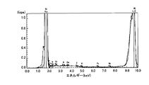
- the impurities on the surface of the epitaxial wafer 130 of Example 1, Comparative Example 1, and Comparative Example 2 were measured by TXRF. Impurities were reduced on the surface of the epitaxial wafer 130 after hydrogen etching in Example 1 as compared with the surface of Comparative Example 1 in which hydrogen etching was not performed. Therefore, it was found that a high-quality SiC semiconductor device can be manufactured by forming a gate oxide film and an electrode on the epitaxial wafer 130 after hydrogen etching to manufacture a SiC semiconductor device.
- FIG. 10 is a spectrum showing the result of measuring the surface of the SiC semiconductor of Comparative Example 1 by TXRF
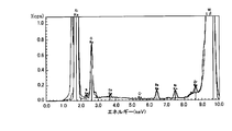
- FIG. 11 is a spectrum showing the result of measuring the surface of the SiC semiconductor of Comparative Example 2 by TXRF.
- the horizontal axis indicates the energy intensity
- the vertical axis indicates the spectrum intensity. The larger the peak height, the more elements are detected.
- “Cl, Ka” written vertically in FIG. 10 indicates that a Cl—K ⁇ ray has been detected, and the same applies to other descriptions.
- the peak in the vicinity of the energy intensity of 9.67 eV is a peak of the WL line that is an excitation ray source.
- the SiC semiconductor of Comparative Example 2 is manufactured by forming an oxide film and an electrode without cleaning the epitaxial wafer 130 after hydrogen etching in Example 1 using a liquid phase and forming an oxide film and an electrode. It has been found that a higher quality SiC semiconductor device can be produced compared to the device.
- SiC substrate 2a surface, 10 manufacturing equipment, 11 removal unit, 12 formation unit, 13 connection unit, 100, 130 epitaxial wafer, 100a, 130a first surface, 100b second surface, 110 gate electrode, 111 source contact Electrode, 112 drain electrode, 120 epitaxial layer, 121 buffer layer, 122 drift layer, 123 body region, 124 source region, 125 p + region, 126 gate oxide film, 127 source electrode, 200 SiC semiconductor device, 201 semiconductor film.
Landscapes
- Engineering & Computer Science (AREA)
- Physics & Mathematics (AREA)
- Microelectronics & Electronic Packaging (AREA)
- General Physics & Mathematics (AREA)
- Manufacturing & Machinery (AREA)
- Computer Hardware Design (AREA)
- Condensed Matter Physics & Semiconductors (AREA)
- Power Engineering (AREA)
- Chemical & Material Sciences (AREA)
- Crystallography & Structural Chemistry (AREA)
- Plasma & Fusion (AREA)
- Electrodes Of Semiconductors (AREA)
- Insulated Gate Type Field-Effect Transistor (AREA)
- Recrystallisation Techniques (AREA)
Priority Applications (5)
| Application Number | Priority Date | Filing Date | Title |
|---|---|---|---|
| KR1020127012240A KR20130076791A (ko) | 2010-06-16 | 2011-02-23 | 탄화규소 반도체 장치의 제조 방법 및 탄화규소 반도체 장치의 제조 장치 |
| CN2011800047820A CN102782820A (zh) | 2010-06-16 | 2011-02-23 | 制造碳化硅半导体器件的方法和装置 |
| EP11795436.2A EP2584594A4 (en) | 2010-06-16 | 2011-02-23 | METHOD FOR PRODUCING A SILICON CARBIDE SEMICONDUCTOR COMPONENT AND DEVICE FOR PRODUCING A SILICON CARBIDE SEMICONDUCTOR COMPONENT |
| CA2779426A CA2779426A1 (en) | 2010-06-16 | 2011-02-23 | Method and apparatus of fabricating silicon carbide semiconductor device |
| US13/503,964 US20120214309A1 (en) | 2010-06-16 | 2011-02-23 | Method and apparatus of fabricating silicon carbide semiconductor device |
Applications Claiming Priority (2)
| Application Number | Priority Date | Filing Date | Title |
|---|---|---|---|
| JP2010136866A JP2012004269A (ja) | 2010-06-16 | 2010-06-16 | 炭化珪素半導体装置の製造方法および炭化珪素半導体装置の製造装置 |
| JP2010-136866 | 2010-06-16 |
Publications (1)
| Publication Number | Publication Date |
|---|---|
| WO2011158528A1 true WO2011158528A1 (ja) | 2011-12-22 |
Family
ID=45347940
Family Applications (1)
| Application Number | Title | Priority Date | Filing Date |
|---|---|---|---|
| PCT/JP2011/054010 WO2011158528A1 (ja) | 2010-06-16 | 2011-02-23 | 炭化珪素半導体装置の製造方法および炭化珪素半導体装置の製造装置 |
Country Status (8)
Cited By (2)
| Publication number | Priority date | Publication date | Assignee | Title |
|---|---|---|---|---|
| US20140193965A1 (en) * | 2009-08-20 | 2014-07-10 | The Government Of The United States Of America, As Represented By The Secretary Of The Navy | REDUCTION OF BASAL PLANE DISLOCATIONS IN EPITAXIAL SiC USING AN IN-SITU ETCH PROCESS |
| EP2833409A4 (en) * | 2012-03-30 | 2015-11-11 | Hitachi Ltd | SILICON CARBIDE FIELD EFFECT TRANSISTOR |
Families Citing this family (15)
| Publication number | Priority date | Publication date | Assignee | Title |
|---|---|---|---|---|
| JP2012004275A (ja) | 2010-06-16 | 2012-01-05 | Sumitomo Electric Ind Ltd | 炭化珪素半導体装置の製造方法 |
| US8860040B2 (en) | 2012-09-11 | 2014-10-14 | Dow Corning Corporation | High voltage power semiconductor devices on SiC |
| US9018639B2 (en) | 2012-10-26 | 2015-04-28 | Dow Corning Corporation | Flat SiC semiconductor substrate |
| JP6162388B2 (ja) * | 2012-11-14 | 2017-07-12 | 新日本無線株式会社 | 炭化珪素半導体装置の製造方法 |
| US9797064B2 (en) | 2013-02-05 | 2017-10-24 | Dow Corning Corporation | Method for growing a SiC crystal by vapor deposition onto a seed crystal provided on a support shelf which permits thermal expansion |
| US9017804B2 (en) | 2013-02-05 | 2015-04-28 | Dow Corning Corporation | Method to reduce dislocations in SiC crystal growth |
| US9738991B2 (en) | 2013-02-05 | 2017-08-22 | Dow Corning Corporation | Method for growing a SiC crystal by vapor deposition onto a seed crystal provided on a supporting shelf which permits thermal expansion |
| US8940614B2 (en) | 2013-03-15 | 2015-01-27 | Dow Corning Corporation | SiC substrate with SiC epitaxial film |
| JP6206012B2 (ja) * | 2013-09-06 | 2017-10-04 | 住友電気工業株式会社 | 炭化珪素半導体装置 |
| JP6222771B2 (ja) | 2013-11-22 | 2017-11-01 | 国立研究開発法人産業技術総合研究所 | 炭化珪素半導体装置の製造方法 |
| US9279192B2 (en) | 2014-07-29 | 2016-03-08 | Dow Corning Corporation | Method for manufacturing SiC wafer fit for integration with power device manufacturing technology |
| JP6314965B2 (ja) * | 2015-12-11 | 2018-04-25 | トヨタ自動車株式会社 | 半導体装置の製造方法 |
| EP4266354B1 (en) * | 2020-12-18 | 2025-04-16 | Kyoto University | Sic semiconductor element manufacturing method |
| JP7669310B2 (ja) * | 2022-03-16 | 2025-04-28 | 株式会社東芝 | 半導体装置の製造方法、半導体装置、インバータ回路、駆動装置、車両、及び、昇降機 |
| IT202300010203A1 (it) * | 2023-05-19 | 2024-11-19 | Consiglio Nazionale Ricerche | Un transistor di potenza per un dispositivo a semiconduttore |
Citations (7)
| Publication number | Priority date | Publication date | Assignee | Title |
|---|---|---|---|---|
| JPH04354334A (ja) | 1991-05-31 | 1992-12-08 | Tadahiro Omi | 半導体の洗浄方法及び洗浄装置 |
| JPH06314679A (ja) | 1993-04-30 | 1994-11-08 | Sony Corp | 半導体基板の洗浄方法 |
| JPH0851110A (ja) * | 1994-08-05 | 1996-02-20 | Matsushita Electric Ind Co Ltd | 絶縁膜の形成方法 |
| JPH10261615A (ja) * | 1997-03-17 | 1998-09-29 | Fuji Electric Co Ltd | SiC半導体の表面モホロジー制御方法およびSiC半導体薄膜の成長方法 |
| JP2000349081A (ja) * | 1999-06-07 | 2000-12-15 | Sony Corp | 酸化膜形成方法 |
| JP2006351744A (ja) * | 2005-06-15 | 2006-12-28 | Fuji Electric Holdings Co Ltd | 炭化珪素半導体装置の製造方法 |
| JP2007053227A (ja) * | 2005-08-18 | 2007-03-01 | Matsushita Electric Ind Co Ltd | 半導体素子およびその製造方法 |
Family Cites Families (15)
| Publication number | Priority date | Publication date | Assignee | Title |
|---|---|---|---|---|
| JPS6066866A (ja) * | 1983-09-24 | 1985-04-17 | Sharp Corp | 炭化珪素mos構造の製造方法 |
| US5787104A (en) * | 1995-01-19 | 1998-07-28 | Matsushita Electric Industrial Co., Ltd. | Semiconductor light emitting element and method for fabricating the same |
| JPH0952796A (ja) * | 1995-08-18 | 1997-02-25 | Fuji Electric Co Ltd | SiC結晶成長方法およびSiC半導体装置 |
| JP3085272B2 (ja) * | 1997-12-19 | 2000-09-04 | 富士電機株式会社 | 炭化けい素半導体装置の熱酸化膜形成方法 |
| JP2001332508A (ja) * | 2000-05-23 | 2001-11-30 | Matsushita Electric Ind Co Ltd | 半導体素子の製造方法 |
| JP3534056B2 (ja) * | 2000-08-31 | 2004-06-07 | 日産自動車株式会社 | 炭化珪素半導体装置の製造方法 |
| US7081420B2 (en) * | 2002-03-19 | 2006-07-25 | Central Research Institute Of Electric Power Industry | Method for preparing SiC crystal and SiC crystal |
| JP2006321707A (ja) * | 2005-04-22 | 2006-11-30 | Bridgestone Corp | 炭化ケイ素単結晶ウェハ及びその製造方法 |
| US8895410B2 (en) * | 2005-09-13 | 2014-11-25 | Tadahiro Ohmi | Method of manufacturing semiconductor device and semiconductor manufacturing apparatus |
| JP2008098200A (ja) * | 2006-10-05 | 2008-04-24 | Kiyoyoshi Mizuno | 成膜体およびその製造方法 |
| US7781312B2 (en) * | 2006-12-13 | 2010-08-24 | General Electric Company | Silicon carbide devices and method of making |
| JP5509520B2 (ja) * | 2006-12-21 | 2014-06-04 | 富士電機株式会社 | 炭化珪素半導体装置の製造方法 |
| JP5125095B2 (ja) * | 2006-12-22 | 2013-01-23 | パナソニック株式会社 | SiCエピタキシャル膜付き基板の製造方法及びSiCエピタキシャル膜付き基板の製造装置 |
| JP5095253B2 (ja) * | 2007-03-30 | 2012-12-12 | 富士通株式会社 | 半導体エピタキシャル基板、化合物半導体装置、およびそれらの製造方法 |
| EP2395133B1 (en) * | 2009-01-30 | 2020-03-04 | Showa Denko K.K. | Method for producing epitaxial silicon carbide single crystal substrate |
-
2010
- 2010-06-16 JP JP2010136866A patent/JP2012004269A/ja active Pending
-
2011
- 2011-02-23 EP EP11795436.2A patent/EP2584594A4/en not_active Withdrawn
- 2011-02-23 KR KR1020127012240A patent/KR20130076791A/ko not_active Withdrawn
- 2011-02-23 CA CA2779426A patent/CA2779426A1/en not_active Abandoned
- 2011-02-23 WO PCT/JP2011/054010 patent/WO2011158528A1/ja active Application Filing
- 2011-02-23 US US13/503,964 patent/US20120214309A1/en not_active Abandoned
- 2011-02-23 CN CN2011800047820A patent/CN102782820A/zh active Pending
- 2011-05-10 TW TW100116378A patent/TW201203391A/zh unknown
Patent Citations (7)
| Publication number | Priority date | Publication date | Assignee | Title |
|---|---|---|---|---|
| JPH04354334A (ja) | 1991-05-31 | 1992-12-08 | Tadahiro Omi | 半導体の洗浄方法及び洗浄装置 |
| JPH06314679A (ja) | 1993-04-30 | 1994-11-08 | Sony Corp | 半導体基板の洗浄方法 |
| JPH0851110A (ja) * | 1994-08-05 | 1996-02-20 | Matsushita Electric Ind Co Ltd | 絶縁膜の形成方法 |
| JPH10261615A (ja) * | 1997-03-17 | 1998-09-29 | Fuji Electric Co Ltd | SiC半導体の表面モホロジー制御方法およびSiC半導体薄膜の成長方法 |
| JP2000349081A (ja) * | 1999-06-07 | 2000-12-15 | Sony Corp | 酸化膜形成方法 |
| JP2006351744A (ja) * | 2005-06-15 | 2006-12-28 | Fuji Electric Holdings Co Ltd | 炭化珪素半導体装置の製造方法 |
| JP2007053227A (ja) * | 2005-08-18 | 2007-03-01 | Matsushita Electric Ind Co Ltd | 半導体素子およびその製造方法 |
Non-Patent Citations (1)
| Title |
|---|
| See also references of EP2584594A4 |
Cited By (4)
| Publication number | Priority date | Publication date | Assignee | Title |
|---|---|---|---|---|
| US20140193965A1 (en) * | 2009-08-20 | 2014-07-10 | The Government Of The United States Of America, As Represented By The Secretary Of The Navy | REDUCTION OF BASAL PLANE DISLOCATIONS IN EPITAXIAL SiC USING AN IN-SITU ETCH PROCESS |
| US10256094B2 (en) * | 2009-08-20 | 2019-04-09 | The Government Of The United States Of America, As Represented By The Secretary Of The Navy | Reduction of basal plane dislocations in epitaxial SiC using an in-situ etch process |
| EP2833409A4 (en) * | 2012-03-30 | 2015-11-11 | Hitachi Ltd | SILICON CARBIDE FIELD EFFECT TRANSISTOR |
| US9214516B2 (en) | 2012-03-30 | 2015-12-15 | Hitachi, Ltd. | Field effect silicon carbide transistor |
Also Published As
| Publication number | Publication date |
|---|---|
| JP2012004269A (ja) | 2012-01-05 |
| EP2584594A1 (en) | 2013-04-24 |
| CN102782820A (zh) | 2012-11-14 |
| TW201203391A (en) | 2012-01-16 |
| KR20130076791A (ko) | 2013-07-08 |
| EP2584594A4 (en) | 2014-07-23 |
| US20120214309A1 (en) | 2012-08-23 |
| CA2779426A1 (en) | 2011-12-22 |
Similar Documents
| Publication | Publication Date | Title |
|---|---|---|
| WO2011158528A1 (ja) | 炭化珪素半導体装置の製造方法および炭化珪素半導体装置の製造装置 | |
| US8642476B2 (en) | Method for manufacturing silicon carbide semiconductor device | |
| US20120178259A1 (en) | Method of cleaning silicon carbide semiconductor and apparatus for cleaning silicon carbide semiconductor | |
| US20130045592A1 (en) | Method for manufacturing silicon carbide semiconductor device and device for manufacturing silicon carbide semiconductor device | |
| JP5605005B2 (ja) | 炭化珪素半導体装置の製造方法および炭化珪素半導体装置の製造装置 | |
| CN101336473A (zh) | 制造碳化硅半导体器件的方法 | |
| CN101652835A (zh) | 具有碳化硅基板的半导体器件的退火方法和半导体器件 | |
| TW200926303A (en) | Semiconductor device manufacturing method and semiconductor device | |
| US20110309376A1 (en) | Method of cleaning silicon carbide semiconductor, silicon carbide semiconductor, and silicon carbide semiconductor device | |
| US20120174944A1 (en) | Cleaning method for silicon carbide semiconductor and cleaning apparatus for silicon carbide semiconductor | |
| JP2011023431A (ja) | 炭化珪素半導体装置の製造方法 | |
| JP5971718B2 (ja) | 半導体装置製造方法 | |
| JP4027913B2 (ja) | 半導体装置の製造方法 |
Legal Events
| Date | Code | Title | Description |
|---|---|---|---|
| WWE | Wipo information: entry into national phase |
Ref document number: 201180004782.0 Country of ref document: CN |
|
| 121 | Ep: the epo has been informed by wipo that ep was designated in this application |
Ref document number: 11795436 Country of ref document: EP Kind code of ref document: A1 |
|
| WWE | Wipo information: entry into national phase |
Ref document number: 13503964 Country of ref document: US |
|
| WWE | Wipo information: entry into national phase |
Ref document number: 2779426 Country of ref document: CA Ref document number: 2011795436 Country of ref document: EP |
|
| ENP | Entry into the national phase |
Ref document number: 20127012240 Country of ref document: KR Kind code of ref document: A |
|
| NENP | Non-entry into the national phase |
Ref country code: DE |