WO2011155313A1 - 現像装置および画像形成装置 - Google Patents
現像装置および画像形成装置 Download PDFInfo
- Publication number
- WO2011155313A1 WO2011155313A1 PCT/JP2011/061764 JP2011061764W WO2011155313A1 WO 2011155313 A1 WO2011155313 A1 WO 2011155313A1 JP 2011061764 W JP2011061764 W JP 2011061764W WO 2011155313 A1 WO2011155313 A1 WO 2011155313A1
- Authority
- WO
- WIPO (PCT)
- Prior art keywords
- waveform
- image
- developer
- developing
- carrier
- Prior art date
- Legal status (The legal status is an assumption and is not a legal conclusion. Google has not performed a legal analysis and makes no representation as to the accuracy of the status listed.)
- Ceased
Links
Images





Classifications
-
- G—PHYSICS
- G03—PHOTOGRAPHY; CINEMATOGRAPHY; ANALOGOUS TECHNIQUES USING WAVES OTHER THAN OPTICAL WAVES; ELECTROGRAPHY; HOLOGRAPHY
- G03G—ELECTROGRAPHY; ELECTROPHOTOGRAPHY; MAGNETOGRAPHY
- G03G15/00—Apparatus for electrographic processes using a charge pattern
- G03G15/06—Apparatus for electrographic processes using a charge pattern for developing
- G03G15/08—Apparatus for electrographic processes using a charge pattern for developing using a solid developer, e.g. powder developer
- G03G15/09—Apparatus for electrographic processes using a charge pattern for developing using a solid developer, e.g. powder developer using magnetic brush
- G03G15/0907—Apparatus for electrographic processes using a charge pattern for developing using a solid developer, e.g. powder developer using magnetic brush with bias voltage
-
- G—PHYSICS
- G03—PHOTOGRAPHY; CINEMATOGRAPHY; ANALOGOUS TECHNIQUES USING WAVES OTHER THAN OPTICAL WAVES; ELECTROGRAPHY; HOLOGRAPHY
- G03G—ELECTROGRAPHY; ELECTROPHOTOGRAPHY; MAGNETOGRAPHY
- G03G15/00—Apparatus for electrographic processes using a charge pattern
- G03G15/06—Apparatus for electrographic processes using a charge pattern for developing
- G03G15/065—Arrangements for controlling the potential of the developing electrode
-
- G—PHYSICS
- G03—PHOTOGRAPHY; CINEMATOGRAPHY; ANALOGOUS TECHNIQUES USING WAVES OTHER THAN OPTICAL WAVES; ELECTROGRAPHY; HOLOGRAPHY
- G03G—ELECTROGRAPHY; ELECTROPHOTOGRAPHY; MAGNETOGRAPHY
- G03G15/00—Apparatus for electrographic processes using a charge pattern
- G03G15/06—Apparatus for electrographic processes using a charge pattern for developing
- G03G15/08—Apparatus for electrographic processes using a charge pattern for developing using a solid developer, e.g. powder developer
- G03G15/0806—Apparatus for electrographic processes using a charge pattern for developing using a solid developer, e.g. powder developer on a donor element, e.g. belt, roller
-
- G—PHYSICS
- G03—PHOTOGRAPHY; CINEMATOGRAPHY; ANALOGOUS TECHNIQUES USING WAVES OTHER THAN OPTICAL WAVES; ELECTROGRAPHY; HOLOGRAPHY
- G03G—ELECTROGRAPHY; ELECTROPHOTOGRAPHY; MAGNETOGRAPHY
- G03G2215/00—Apparatus for electrophotographic processes
- G03G2215/06—Developing structures, details
- G03G2215/0634—Developing device
- G03G2215/0636—Specific type of dry developer device
- G03G2215/0648—Two or more donor members
Definitions
- the present invention relates to an image forming apparatus using an electrophotographic system such as a copying machine, a printer or a facsimile machine, and a developing device used for developing an electrostatic latent image formed on an image carrier in the image forming apparatus. .
- Patent Document 1 JP-A-6-348117
- Patent Document 2 JP-A-2000-56547
- Patent Document 3 JP-A-2005-309265
- Patent Document 4 JP 2009-168893
- a developing method for visualizing (developing) an electrostatic latent image on a photoconductor a one-component developing method, a two-component developing method, and a hybrid developing method (hereinafter, referred to as an HBD developing method).
- HBD developing method a hybrid developing method
- toner and carrier are used as the two-component developer.
- the toner is quickly and stably charged by contact and friction with the carrier.
- the system speed is increased, carriers are likely to fly and adhere to the photoreceptor, and image noise such as carrier fog is likely to occur.
- the HBD development method has a configuration in which a one-component development method and a two-component development method are combined.
- the replenished toner is mixed and stirred with the carrier.
- the toner is quickly and stably charged. Therefore, there is a merit that the stress applied to the toner is smaller than that in the one-component developing method in which charging is performed at the regulating portion.
- development is performed by forming a toner layer on the developing roller using an electric field. Therefore, even when the system speed is increased, no carrier fog occurs because no carrier exists in the developing unit.
- Patent Document 5 discloses an image forming apparatus in which two developing rollers are arranged to face each other on one photoconductor (image carrier).
- the developing unit the region between the surface of the image carrier on which the electrostatic charge image is formed and the developing roller
- development is performed.
- an image forming apparatus in which two developing rollers are disposed opposite to one photoconductor ensures a longer developing section as compared to an image forming apparatus in which one developing roller is disposed opposite to one photoconductor. Can do. Even when the system speed of the image forming apparatus increases (for example, during high-speed printing), sufficient time can be conveyed to the photoconductor by increasing the facing time between the photoconductor and the developing roller. It becomes possible.
- the potential of the electrostatic latent image on the photosensitive member is a low density potential (a potential for forming a low density image)
- the present invention has been made in view of the above, and is a developing device and an image forming apparatus in which two developing rollers are opposed to one photoconductor, and an optimum image density is obtained even at a low density potential. It is an object of the present invention to provide a developing device and an image forming apparatus that can perform the above operation.
- a developing device is a developing device for developing an electrostatic latent image formed on an image carrier with toner, and the first development is arranged to face the image carrier.
- a first voltage applying unit that applies a first development bias voltage of a rectangular wave in which an AC voltage is superimposed on a DC voltage to one of the agent carrier and the second developer carrier; the first developer carrier;
- a second voltage applying section for applying a second developing bias voltage in which an alternating voltage is superimposed on a direct current voltage, on the other side of the second developer carrier, and the waveform of the alternating voltage in the second developing bias voltage.
- a developing device is the developing device according to the first aspect, wherein the waveform of the alternating voltage in the second developing bias voltage is the toner supplied to the first developer carrier or the developer.
- a development-side peak portion for supplying the image from the second developer carrier to the image carrier; a recovery-side peak portion for returning the toner from the image carrier to the first developer carrier or the second developer carrier;
- a voltage change portion during the transition from the development side peak portion to the recovery side peak portion, and the waveform at the voltage change portion starts from the end of the development side peak portion as the starting point. It is inclined toward the part.
- the developing device is the developing device according to the first aspect, wherein the waveform of the alternating voltage in the second developing bias voltage is the toner supplied to the first developer carrier or the developer.
- a development-side peak portion for supplying the image from the second developer carrier to the image carrier; a recovery-side peak portion for returning the toner from the image carrier to the first developer carrier or the second developer carrier;
- a voltage change portion during the transition from the development side peak portion to the recovery side peak portion, and the waveform in the voltage change portion has a blank pulse time in which the potential difference is zero.
- the developing device according to the fourth aspect of the present invention is the developing device according to the third aspect, wherein the blank pulse time is about 0.02 ms or more and about 0.06 ms or less.
- a developing device is the developing device according to any one of the first to fourth aspects, wherein the developing device faces the first developer carrier and the second developer carrier. And a conveyance member that carries the developer including the toner and the carrier and supplies the toner in the developer to the first developer carrier and the second developer carrier.
- An image forming apparatus includes the image carrier, an image forming mechanism for forming an electrostatic latent image on the image carrier, and a developing device according to any one of the first to fourth aspects. It is equipped with.
- a developing device and an image forming apparatus in which two developing rollers are opposed to one photoconductor, and the developing device and the image forming capable of obtaining an optimum image density even at a low density potential.
- a device can be obtained.
- FIG. 3 is a perspective view illustrating an appearance of an image forming apparatus according to Embodiment 1 and Embodiment 2.
- FIG. 2 is a cross-sectional view schematically showing an image forming unit including the developing device in Embodiment 1.
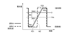
- FIG. FIG. 6 is a first diagram illustrating a waveform of a voltage (potential difference) applied as a developing bias in the developing device according to the experimental example of the first embodiment and the second embodiment.
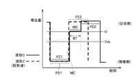
- FIG. 12 is a second diagram illustrating a waveform of a voltage (potential difference) applied as a developing bias in the developing device according to the experimental example of the first embodiment and the second embodiment.
- FIG. 10 is a third diagram showing a waveform of a voltage (potential difference) applied as a developing bias in the developing device according to the experimental example of the first embodiment and the second embodiment.
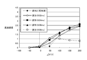
- FIG. 6 is a first diagram showing a measurement result of an experimental example performed using the developing device in the first embodiment.
- FIG. 10 is a second diagram showing measurement results of an experimental example performed using the developing device according to the first embodiment.
- FIG. 10 is a third diagram showing the measurement results of an experimental example performed using the developing device in the first embodiment. 6 is a cross-sectional view schematically showing an image forming unit including a developing device in Embodiment 2.
- FIG. FIG. 10 is a diagram showing a measurement result of an experimental example performed using the developing device according to the second embodiment.
- the image forming apparatus 1000 is an example of an image forming apparatus such as a copying machine, a printer, or a facsimile.
- the image forming apparatus 1000 includes an operation unit 51 and an operation display 52 in an operation panel 50 located at the top of the main body.
- the operation unit 51 receives various instructions and the like from the user input through the key 51a.
- the operation display 52 displays an instruction menu for the user.
- a scanner 53 and a feeder 55 are provided on the upper surface of the main body.
- the feeder 55 sends the document to the scanner 53.
- a printer 54 is provided on the side of the main body.
- a tray 57 and a paper feeding unit 58 are provided at the lower part of the main body.
- a recording sheet on which an image is printed by the printer 54 is discharged to the tray 57.
- the paper supply unit 58 supplies the recording sheet to the printer 54.
- An image forming unit 100 is provided inside the main body. The image forming unit 100 prints an image on a recording sheet.
- FIG. 2 is a cross-sectional view schematically showing details of the image forming unit 100.
- the image forming unit 100 includes a developing device 2A (first developing device) and a developing device 2B (second developing device) in the present embodiment.
- first developing device first developing device
- developing device 2B second developing device
- the image forming unit 100 employs a one-component developing method as a developing method.
- the image forming unit 100 can be mounted in an electrophotographic image forming apparatus (for example, the image forming apparatus 1000 in FIG. 1) such as a copying machine, a printer, or a facsimile.
- the image forming unit 100 includes an image carrier 1, a transfer unit 4, a cleaning unit 5, a charging unit 6, an exposure unit 7, a developing device 2A, a developing device 2B, and an image density detecting unit 33.
- the transfer unit 4, the cleaning unit 5, the charging unit 6, the exposure unit 7, the developing device 2 ⁇ / b> A, the developing device 2 ⁇ / b> B, and the image density detection unit 33 are arranged around the image carrier 1 in the rotation direction (arrow R ⁇ b> 1). (Direction).
- the operation of the image forming unit 100 will be described.
- the image carrier 1 as a photosensitive member rotates in the direction of arrow R1. As the image carrier 1 rotates, the surface of the image carrier 1 is uniformly charged by the charging unit 6. A surface potential (Vo) is applied to the image carrier 1.
- the exposure unit 7 receives an image signal from a digital image processing unit (not shown), modulates the laser, and irradiates the surface of the image carrier 1 with the modulated laser L. The surface of the image carrier 1 is exposed by the laser L irradiation, and an electrostatic latent image (not shown) is formed on the surface of the image carrier 1.
- each developing method is a one-component developing method.
- the developing devices 2 ⁇ / b> A and 2 ⁇ / b> B convey the developer 25 (toner) to the electrostatic latent image formed on the surface of the image carrier 1.
- the electrostatic latent image is developed (visualized) as a toner image by the developer 25.
- the developing roller 20A (first developer carrier) in the developing device 2A is opposed to the image carrier 1 with a predetermined gap (gap).
- the developing roller 20B (second developer carrier) in the developing device 2B is also opposed to the image carrier 1 with a predetermined interval.
- the developing roller 20B is located downstream of the developing roller 20A in the rotation direction (arrow R1 direction) of the image carrier 1.
- the developing devices 2A and 2B have substantially the same configuration.
- the configuration and operation of the developing devices 2A and 2B other than the developing rollers 20A and 20B will be described based on only the developing device 2A as a representative. Since the developing device 2B overlaps, the description thereof will not be repeated.
- the replenishing toner 27 in the toner replenishing unit 28 is conveyed to the mixing and stirring tank 26 through the replenishing toner conveying member 29.
- the replenishment toner 27 is mixed with the developer 25 in the mixing and stirring tank 26 and then conveyed to the developer conveying roller 22 through the developer conveying members 24a and 24b.
- the developer 25 and the replenishment toner 27 (hereinafter simply referred to as developer 25) are both one-component developers and are powders made of toner.
- the toner may be negatively charged or positively charged.
- the toner is charged by friction with the developer layer regulating member 21.
- the toner can be produced by using a general method (such as a pulverization method, an emulsion polymerization method, or a suspension polymerization method).
- a predetermined voltage is applied by the voltage application unit 31 to the developing roller 20A rotating in the direction of arrow R20A (developing roller 20B rotating in the direction of arrow R20B).
- a predetermined voltage is applied by the voltage application unit 32 to the developer transport roller 22 that rotates in the direction of the arrow R22. By applying this voltage, the developer 25 is conveyed from the developer conveying roller 22 to the developing roller 20A. The amount (layer thickness) of the developer 25 conveyed on the developing roller 20A is adjusted by the developer layer regulating member 21.
- a developing bias (developing bias voltage) in which an AC voltage is superimposed on a DC voltage is applied by the voltage applying unit 31 to the developing roller 20A that has received the developer 25.
- the developer 25 flies from the developing roller 20 ⁇ / b> A toward the image carrier 1.
- the developer 25 is conveyed onto the electrostatic latent image formed on the image carrier 1 by irradiation with the laser L.
- the electrostatic latent image is developed (visualized) as a toner image.
- the toner image formed on the surface of the image carrier 1 is transferred to the recording medium 8 by the transfer unit 4.
- the developer 25 transferred to the recording medium 8 is fixed on the recording medium 8 after being applied heat or pressure by a fixing device (not shown) or the like.
- the toner image formed on the surface of the image carrier 1 is removed from the image carrier 1 by the cleaning unit 5 such as a cleaning blade after passing through the transfer unit 4 by the rotation of the image carrier 1.
- the surface of the image carrier 1 from which the toner image has been removed is conveyed again to the charging unit 6 and is used for developing other toner images.
- the image density of the visualized developer 25 on the recording medium 8 may be detected by the image density detector 33.
- image forming conditions are set according to the detected image density.
- the output voltage of the voltage application unit 31 may be controlled based on the image forming conditions.
- the developing rollers 20 ⁇ / b> A and 20 ⁇ / b> B are disposed to face one image carrier 1.
- the image forming unit 100 can ensure a longer development time compared to the case where one developing roller is disposed opposite to one image carrier (photosensitive member). Even during high-speed printing, the facing time between the image carrier 1 and the developing rollers 20A and 20B becomes long. Sufficient toner can be conveyed to the image carrier 1.
- the image forming unit 100 is configured such that a toner image is directly transferred from the image carrier 1 to the recording medium 8. As another configuration, after the toner image is once transferred to an intermediate transfer member (not shown), the toner image may be transferred to the recording medium 8 after superposing other colors.
- Each setting condition in the experimental example is as follows.
- the system speed of the image forming unit 100 was about 300 mm / s.
- Metalme registered trademark (made by Toray Industries, Inc.) made of an aluminum-deposited PET film having a thickness of about 30 ⁇ m was used. .
- An electrostatic latent image was formed on the surface of the image carrier 1 by water charging. In water charging, water dripped on the surface of the image carrier 1 and the teeth of the cutter are brought into contact. A voltage is applied in this state. An electrostatic latent image is formed on the surface of the image carrier 1 by applying a surface potential (Vi) corresponding to the applied voltage to the surface of the image carrier 1.
- the surface potential Vi in the electrostatic latent image is about ⁇ 350V to 0V.
- the developing rollers 20A and 20B aluminum rollers having an alumite treatment on the surface were used.
- the distance between the developing rollers 20A and 20B and the image carrier 1 was set to be about 250 ⁇ m at the closest part.
- the conveyance amount of the developer 25 on the developing rollers 20A and 20B was about 6 g / m 2 .
- waveform Z and waveforms A to D were prepared for five types of development bias.
- the potential difference indicated by the vertical axis in each figure indicates the relative potential difference between the developing rollers 20A and 20B with respect to the image carrier 1 when the image carrier 1 is grounded.
- details of the waveform Z and the waveforms A to D will be described in order.
- Waveform Z Rectangular wave
- Waveform Z includes a development-side peak portion PZ1 that urges the developer from the developing roller toward the image carrier, a collection-side peak portion PZ2 that urges the developer from the image carrier to the development roller, and the development side.
- a voltage changing portion MZ that transitions from the peak portion PZ1 to the recovery-side peak portion PZ2 is periodically provided.
- the DC component Vdc is ⁇ 350 V
- the amplitude (Peak to Peak) is 2250 V
- the duty ratio the working time of the voltage on the developing side for supplying the developer to the image carrier, the developer
- the ratio of the voltage on the collecting side to be returned to the developing roller is 50%
- the frequency is 5 kHz.
- the potential difference at the development side peak portion PZ1 is ⁇ 1475V
- the potential difference at the recovery side peak portion PZ2 is 775V.
- the potential difference changes vertically from the development side peak part PZ1 toward the recovery side peak part PZ2.
- the waveform Z in the voltage change portion MZ rises vertically, and the developing bias operating time in the voltage change portion MZ is substantially 0 second.
- Waveform A With continuing reference to FIG. 3, a waveform A indicated by a solid line in the drawing is a modification of the above-described typical rectangular wave (waveform Z).
- Waveform A includes a development-side peak portion PA1 that biases the developer from the developing roller toward the image carrier, a recovery-side peak portion PA2 that biases the developer from the image carrier toward the development roller, and the development side.
- a voltage changing unit MA that transitions from the peak part PA1 to the recovery-side peak part PA2 is periodically provided.
- the working time of the developing bias with respect to the frequency (1 period) of 5 kHz is about 30% at the developing side peak portion PA1, about 30% at the collecting side peak portion PA2, and about 40% at the voltage changing portion MA.
- the potential difference changes obliquely from the development side peak part PA1 toward the recovery side peak part PA2.
- the waveform A in the voltage change portion MA is inclined so that the potential difference gradually increases (in the positive direction) in both the first half MA1 (rising portion) of the voltage change portion MA and the second half MA2 of the voltage change portion MA. ing.
- Other portions amplitude, potential difference at the development-side peak portion, potential difference at the collection-side peak portion, etc. are the same as those of the waveform Z.
- Waveform B Referring to FIG. 4, a waveform B indicated by a solid line in the drawing is also a modification of the above-described typical rectangular wave (waveform Z).
- Waveform B includes a development-side peak portion PB1 that urges the developer from the developing roller toward the image carrier, a recovery-side peak portion PB2 that urges the developer from the image carrier toward the development roller, and the development side.
- a voltage change unit MB that transitions from the peak part PB1 to the recovery-side peak part PB2 is periodically provided.
- the working time of the developing bias with respect to the frequency (one cycle) of 5 kHz is about 50% at the developing side peak portion PB1, about 30% at the collecting side peak portion PB2, and about 20% at the voltage changing portion MB.
- the potential difference changes vertically from the development side peak part PB1 toward the potential difference equivalent to the DC component Vdc from the start point.
- the waveform B in the voltage change part MB rises vertically (substantially the operation time is 0 second) in the first half MB1 (rise part) of the voltage change part MB, and the potential difference gradually increases only in the second half part MB2 of the voltage change part MB. It is inclined so as to increase (in the positive direction). Other portions are substantially the same as the waveform Z.
- Waveform C With continuing reference to FIG. 4, the waveform C indicated by the dotted line in the figure is also a modification of the above-described typical rectangular wave (waveform Z).
- Waveform C includes a development-side peak portion PC1 that urges the developer from the developing roller toward the image carrier, a collection-side peak portion PC2 that urges the developer from the image carrier toward the development roller, and the development side.
- a voltage change unit MC that transitions from the peak portion PC1 to the recovery-side peak portion PC2 is periodically provided.
- the working time of the developing bias with respect to the frequency (one cycle) of 5 kHz is about 30% at the developing side peak portion PC1, about 50% at the collecting side peak portion PC2, and about 20% at the voltage changing portion MC.
- a potential difference equivalent to the DC component Vdc is set as a starting point, and the potential difference is vertically changed from the starting point toward the recovery side peak part PC2.
- the waveform C in the voltage change part MC is inclined so that the potential difference gradually increases (in the positive direction) in the first half MC1 (rising part) of the voltage change part MC, and in the second half MC2 of the voltage change part MC. Stands up vertically (actually 0 time of action). Other portions are substantially the same as the waveform Z.
- Waveform D a development bias waveform D indicated by a solid line in FIG. 5 is also a modification of the above-described typical rectangular wave (waveform Z).
- FIG. 5 also shows a waveform Z for convenience of explanation.
- Waveform D includes a development-side peak portion PD1 that urges the developer from the developing roller toward the image carrier, a recovery-side peak portion PD2 that urges the developer from the image carrier to the development roller, and the development side.
- a voltage change part MD that shifts from the peak part PD1 to the recovery-side peak part PD2 is periodically provided.
- the working time of the developing bias at the developing side peak portion PD1 of the waveform D is equal to the working time of the developing bias at the developing side peak portion PZ1 of the waveform Z.
- the working time of the developing bias at the collection-side peak portion PD2 of the waveform D is equal to the working time of the developing bias at the collecting-side peak portion PZ2 of the waveform Z.
- the waveform D in the voltage change part MD is a blank pulse (potential difference is about 0 V) with a blank pulse time BT of about 0.02 msec to about 0.08 msec. Other portions are substantially the same as the waveform Z. Details of the range of the blank pulse time BT will be described later.
- the developing bias applied to the developing roller 20A was a waveform Z (rectangular wave).
- the developing bias applied to the developing roller 20B was one of the waveforms Z and A to C.
- ) and the image density in the obtained image was measured.
- “310TR” manufactured by X-Rite was used, and the transmission density was measured.
- FIG. 6 shows the measurement results in this experiment for each of the developing bias waveforms Z, A to C applied to the developing roller 20B.
- the lines indicated as waveforms Z and A to C indicate the measurement results of the experiment when the developing bias applied to the developing roller 20B is the waveforms Z and A to C, respectively.
- the developing bias applied to the developing roller 20A was a waveform Z (rectangular wave).
- the developing bias applied to the developing roller 20B was each of four types of waveforms D having different waveforms Z and blank pulse times BT. Also in this experiment, the relationship between the image potential ⁇ V (
- FIG. 7 shows the experiment for each waveform (0.02 ms), waveform (0.04 ms), waveform (0.06 ms), and waveform (0.08 ms) based on the waveform D applied to the developing roller 20B.
- the measurement result in is shown.
- the line shown as the waveform Z indicates the measurement result of the experiment when the developing bias applied to the developing roller 20B is the waveform Z (equivalent to the line shown as the waveform Z in FIG. 6).
- lines indicated as a waveform (0.02 ms), a waveform (0.04 ms), a waveform (0.06 ms), and a waveform (0.08 ms) indicate the development bias applied to the developing roller 20B as the waveform D.
- the measurement results of the experiment when the blank pulse time BT (see FIG. 5) is 0.02 ms, 0.04 ms, 0.06 ms, and about 0.08 ms are shown.
- the following can be seen at a low concentration potential (for example, about 50 V to about 100 V).
- a low concentration potential for example, about 50 V to about 100 V.
- the case where the developing bias based on the waveform D having a blank pulse time BT of about 0.02 ms to about 0.08 ms is applied to the developing roller 20B.
- a high image density (transmission density) can be obtained at a low density potential.
- a developing bias based on the waveform D having a blank pulse time BT of 0.08 ms or more is applied to the developing roller 20B, a very high image density cannot be obtained at a high density potential, so another measure is taken. I found it necessary. Therefore, it is desirable that the blank pulse time BT is about 0.02 ms or more and about 0.06 ms or less.
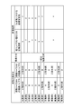
- FIG. 8 collectively shows the measurement results described above and the experimental results further performed based on the measurement results as Comparative Examples 1 to 7 and Examples 1 to 6.
- the developing bias applied to the developing rollers 20A and 20B is set as various combinations of the waveform Z and the waveforms A to D under the same setting conditions as described above. Yes.
- the waveform D since the results when the blank pulse time BT (see FIG. 5) is 0.02 ms, 0.04 ms, 0.06 ms, and 0.08 ms are the same, these are collectively shown.
- FIG. 8 shows whether or not a desired image density is obtained at a low density potential.
- a state where the image density is high is shown as a symbol Y, and a state where the image density is low is shown as a symbol X.
- the state where the image density is high is a state where a desired image density is obtained.
- the state where the image density is low is a state where a desired image density is not obtained.
- FIG. 8 also shows the presence / absence of a change in image density (image stability) with respect to Ds change (change in distance at the closest portion between the developing roller and the image carrier).
- a state where image stability is obtained is indicated as symbol Y, and a state where image stability is not obtained is indicated as symbol X.
- the state where the image stability is obtained is a state where there is no change in the image density with respect to the Ds fluctuation.
- the state where the image stability cannot be obtained is a state where there is a change in the image density with respect to the Ds fluctuation.
- the development biases applied to the development rollers 20A and 20B are as follows.
- the developing roller 20A has a waveform Z and the developing roller 20B has a waveform Z.
- the developing roller 20A has a waveform A
- the developing roller 20B has a waveform A.
- the developing roller 20A has a waveform B and the developing roller 20B has a waveform B.
- the developing roller 20A has a waveform C
- the developing roller 20B has a waveform C.
- the developing roller 20A has a waveform D
- the developing roller 20B has a waveform D.
- the developing roller 20A has a waveform B and the developing roller 20B has a waveform Z.
- the developing roller 20A has a waveform Z and the developing roller 20B has a waveform B.
- Example 1 the developing roller 20A has a waveform A and the developing roller 20B has a waveform Z.
- Example 2 the developing roller 20A has a waveform Z, and the developing roller 20B has a waveform A.
- Example 3 the developing roller 20A has a waveform C, and the developing roller 20B has a waveform Z.
- Example 4 the developing roller 20A has a waveform Z, and the developing roller 20B has a waveform C.
- Example 5 the developing roller 20A has a waveform D and the developing roller 20B has a waveform Z.
- Example 6 the developing roller 20A has a waveform Z and the developing roller 20B has a waveform D.
- the developing roller 20A should have the waveform Z (rectangular wave) and the developing roller 20B should have the waveform A, the waveform C, or the waveform D for the developing bias to be applied.
- the developing roller 20B may have a waveform Z (rectangular wave) and the developing roller 20A may have a waveform A, waveform C, or waveform D.
- one of the developing rollers 20A and 20B may have a waveform Z and the other of the developing rollers 20A and 20B may have a waveform A, a waveform C, or a waveform D.
- the waveform A (see FIG. 3) is inclined so that the potential difference gradually increases (in the positive direction) from the development-side peak portion PA1 to the recovery-side peak portion PA2 in the first half MA1 of the voltage change portion MA. is doing.
- the waveform C in the first half MC1 of the voltage change part MC, the potential difference gradually increases in the positive direction from the development side peak part PC1 toward the recovery side peak part PC2 (potential difference equivalent to the DC component Vdc). To be larger.
- Waveforms A and C are inclined so that the potential difference gradually increases (in the positive direction) from the tips of the development side peak portions PA1 and PC1.
- the amount of developer transported from the developing roller to the image carrier gradually decreases. Therefore, the developer (toner) adhering to the image carrier 1 side (on the electrostatic latent image) is knocked out by the developer flying toward the image carrier (electrostatic latent image) later. This is presumed to be due to the fact that it is suppressed (returned from the image bearing member to the developing roller side) (hereinafter referred to as a knock-out phenomenon).
- the waveform D (see FIG. 5) has a voltage change part MD of the blank pulse time BT between the development side peak part PD1 and the recovery side peak part PD2.
- this voltage change part MD since there is no electric field acting on the flying developer, it is possible to reduce the speed of the developer, and the knock-out phenomenon is suppressed as in the case of waveform A or waveform C. It is assumed that there is.
- the waveform Z (see FIG. 3) is a rectangular wave, and in the voltage change portion MZ, the potential difference rises vertically from the development side peak portion PZ1 toward the recovery side peak portion PZ2. In other words, in the waveform Z, the potential difference suddenly changes from the development side peak portion PZ1 to the recovery side peak portion PZ2. Also in the waveform B (see FIG. 4), the potential difference rises vertically from the development side peak portion PB1 toward the recovery side peak portion PB2 (potential difference equivalent to the DC component Vdc) in the first half MB1 of the voltage change portion MB. In other words, also in the waveform B, the potential difference suddenly changes from the development side peak portion PB1 toward the recovery side peak portion PB2 (potential difference equivalent to the DC component Vdc).
- the developing roller 20A has a waveform Z (rectangular wave) and the developing roller 20B has a waveform A, a waveform C, or a waveform D, because the knock-out phenomenon at the subsequent developing roller 20B is suppressed. It is thought that.
- the developing roller 20B has a waveform Z (rectangular wave) and the developing roller 20A has a waveform A, waveform C, or waveform D, the squealing phenomenon at the preceding developing roller 20A is suppressed, but the developing roller at the latter stage Since there is a knockout phenomenon at 20B, it is necessary to attach a sufficient amount of developer to the image carrier 1 with the development roller 20A in the previous stage.
- the image forming unit 100 including the developing devices 2A and 2B by setting one of the developing rollers 20A and 20B to the waveform Z and the other of the developing rollers 20A and 20B to the waveform A or the waveform C, In addition to being able to obtain a high image density even at a low density potential, it is possible to suppress changes in the image density (occurrence of variation, unevenness, etc.) even when Ds fluctuation occurs. The same effect can be obtained also in an image forming apparatus provided with such an image forming unit 100.
- FIG. 9 is a cross-sectional view schematically showing the image forming unit 200.
- the image forming unit 200 includes the developing device 2 in the present embodiment.
- the configuration of the image forming unit 200 will be described.
- the image forming unit 200 employs a hybrid development method as a development method.
- the image forming unit 200 can be mounted in an electrophotographic image forming apparatus (for example, the image forming apparatus 1000 in FIG. 1) such as a copying machine, a printer, or a facsimile.
- the image forming unit 200 includes an image carrier 1, a transfer unit 4, a cleaning unit 5, a charging unit 6, an exposure unit 7, a developing device 2, and an image density detection unit 33.
- the transfer unit 4, the cleaning unit 5, the charging unit 6, the exposure unit 7, the developing device 2, and the image density detection unit 33 are arranged around the image carrier 1 along the rotation direction of the image carrier 1 (arrow R ⁇ b> 1 direction). Are arranged in order.
- the operation of the image forming unit 200 will be described.
- the image carrier 1 as a photosensitive member rotates in the direction of arrow R1. As the image carrier 1 rotates, the surface of the image carrier 1 is uniformly charged by the charging unit 6. A surface potential (Vo) is applied to the image carrier 1.
- the exposure unit 7 receives an image signal from a digital image processing unit (not shown), modulates the laser, and irradiates the surface of the image carrier 1 with the modulated laser L. The surface of the image carrier 1 is exposed by the laser L irradiation, and an electrostatic latent image (not shown) is formed on the surface of the image carrier 1.
- the developing device 2 is a hybrid developing method, and uses a developer 25 containing toner and carrier.
- the electrostatic latent image is developed (visualized) as a toner image by the toner in the developer 25.
- the developing roller 20A (first developer carrier) in the developing device 2 faces the image carrier 1 with a predetermined gap (gap) therebetween.
- the developing roller 20B (second developer carrier) in the developing device 2 is also opposed to the image carrier 1 with a predetermined interval.
- the developing roller 20B is located downstream of the developing roller 20A in the rotation direction (arrow R1 direction) of the image carrier 1.
- the replenishment toner 27 in the toner replenishing unit 28 is conveyed to the mixing and stirring tank 26 through the replenishment toner conveyance member 29.
- the replenishment toner 27 is mixed with the developer 25 including the carrier in the mixing and stirring tank 26 by the developer conveying members 24a and 24b.
- the toner may be negatively charged by friction with the carrier or positively charged.
- the toner can be produced by using a general method (such as a pulverization method, an emulsion polymerization method, or a suspension polymerization method).
- the carrier one having magnetism is used, and a binder type carrier or a coat type carrier can be used.
- the particle size of the carrier is preferably about 15 ⁇ m to about 100 ⁇ m.
- the toner ratio in the developer is preferably in the range of about 5 wt% to about 30 wt%, more preferably about 8 wt%.
- the toner in the developer 25 is frictionally charged by mixing with the carrier.
- the developer 25 is conveyed by the magnet roller 23 (conveying member) using the magnetism of the carrier.
- the magnet roller 23 includes a developer transport roller (sleeve) 22 and a magnetic body 22A provided in the developer transport roller 22 and having a plurality of magnetic poles.
- the amount (layer thickness) of the developer 25 conveyed on the magnet roller 23 is adjusted by the developer layer regulating member 21.
- a predetermined voltage is applied to the magnet roller 23 that conveys the developer 25 in the direction of the arrow R23 by a voltage application unit 32 connected thereto.
- a predetermined voltage is applied to the developing roller 20A rotating in the direction of the arrow R20A by a voltage application unit 31 connected thereto.
- a predetermined voltage is also applied to the developing roller 20B rotating in the direction of the arrow R20B by the voltage applying unit 31 connected thereto.
- a developing bias in which an AC voltage is superimposed on a DC voltage is applied to the developing rollers 20A and 20B that have been supplied with the developer 25 by a voltage applying unit 31.
- the toner flies toward the image carrier 1 from the developing rollers 20A and 20B.
- the toner adheres to the electrostatic latent image on the image carrier 1 formed by the laser L irradiation.
- the electrostatic latent image is developed (visualized) as a toner image.
- the toner image formed on the surface of the image carrier 1 is removed from the image carrier 1 by the cleaning unit 5 such as a cleaning blade after passing through the transfer unit 4 by the rotation of the image carrier 1.
- the surface of the image carrier 1 from which the toner image has been removed is conveyed again to the charging unit 6 and is used for developing other toner images.
- the image density of the visualized developer 25 on the recording medium 8 may be detected by the image density detector 33.
- image forming conditions are set according to the detected image density.
- the output voltage of the voltage application unit 31 may be controlled based on the image forming conditions.
- the developing rollers 20 ⁇ / b> A and 20 ⁇ / b> B are arranged to face one image carrier 1.
- the image forming unit 200 can ensure a longer developing section as compared with a case where one developing roller is disposed opposite to one image carrier (photosensitive member). Even during high-speed printing, the facing time between the image carrier 1 and the developing rollers 20A and 20B becomes long. Sufficient toner can be conveyed to the image carrier 1.
- the image forming unit 200 is configured such that a toner image is directly transferred from the image carrier 1 to the recording medium 8. As another configuration, after the toner image is once transferred to an intermediate transfer member (not shown), the toner image may be transferred to the recording medium 8 after superposing other colors.
- Comparative Examples 1A to 3A and Examples 1A to 6A With reference to FIG. 10, Comparative Examples 1A to 3A and Examples 1A to 6A will be described.
- each of the developing biases applied to the developing rollers 20A and 20B has various combinations of waveform Z and waveforms A to D (see FIGS. 3 to 5).
- FIG. 10 shows whether or not a desired image density is obtained at a low density potential.
- a state where the image density is high is shown as a symbol Y, and a state where the image density is low is shown as a symbol X.
- the definitions of the symbol Y and the symbol X indicating the image density state are the same as in the first embodiment.
- FIG. 10 also shows the presence or absence of a change in image density (image stability) with respect to Ds fluctuation (fluctuation in distance at the closest portion between the developing roller and the image carrier).
- a state in which image stability is obtained is indicated by symbol Y in the figure, and a state in which image stability is not obtained is indicated by symbol X in the figure.
- symbol Y and the symbol X indicating the image stability state are the same as those in the first embodiment.
- the developing biases applied to the developing rollers 20A and 20B are as follows.
- the developing roller 20A has a waveform A, and the developing roller 20B has a waveform A.
- the developing roller 20A has a waveform C, and the developing roller 20B has a waveform C.
- the developing roller 20A has a waveform D, and the developing roller 20B has a waveform D.
- Example 1A the developing roller 20A has a waveform A, and the developing roller 20B has a waveform Z.
- the developing roller 20A has a waveform Z, and the developing roller 20B has a waveform A.
- Example 3A the developing roller 20A has a waveform C, and the developing roller 20B has a waveform Z.
- the developing roller 20A has a waveform Z, and the developing roller 20B has a waveform C.
- Example 5A the developing roller 20A has a waveform D, and the developing roller 20B has a waveform Z.
- Example 6A the developing roller 20A has a waveform Z, and the developing roller 20B has a waveform D.
- the developing roller 20A should have a waveform Z (rectangular wave) and the developing roller 20B should have a waveform A, waveform C, or waveform D. It can also be seen that the developing roller 20B may have a waveform Z (rectangular wave) and the developing roller 20A may have a waveform A, a waveform C, or a waveform D. In other words, it can be seen that one of the developing rollers 20A and 20B may have a waveform Z and the other of the developing rollers 20A and 20B may have a waveform A, a waveform C, or a waveform D.
- This cause is presumed to be the same as that of the one-component developing type image forming apparatus in the first embodiment.
Landscapes
- Physics & Mathematics (AREA)
- General Physics & Mathematics (AREA)
- Developing For Electrophotography (AREA)
- Dry Development In Electrophotography (AREA)
Abstract
Description
(画像形成装置1000)
図1を参照して、本実施の形態における画像形成装置1000について説明する。画像形成装置1000は、複写機、プリンターまたはファクシミリ等の画像形成装置の一例である。画像形成装置1000は、本体の上部に位置する操作パネル50内に、操作部51および操作ディスプレイ52を有している。操作部51は、キー51aを通して入力されたユーザーからの各種の指示等を受け付ける。操作ディスプレイ52は、ユーザーに対する指示メニュー等を表示する。
図2は、画像形成ユニット100の詳細を模式的に示した断面図である。画像形成ユニット100は、本実施の形態における現像装置2A(第1現像装置)および現像装置2B(第2現像装置)を含んでいる。以下、画像形成ユニット100の構成について説明する。
上述の画像形成ユニット100においては、現像剤25を飛翔させるための現像バイアスが最適化されている。以下、この最適化を得るために実施した実験例(実施例および比較例を含む)について説明する。
当該実験例における各設定条件は次の通りである。画像形成ユニット100のシステム速度は約300mm/sとした。像担持体1(図2参照)には、上述した実施の形態1の感光体の代わりに、厚さ約30μmのアルミ蒸着PETフィルムからなるメタルミー(登録商標)(東レ株式会社製)を使用した。
図3を参照して、図中点線によって示される波形Zは、典型的な矩形波である。波形Zは、現像ローラーから像担持体に向けて現像剤を付勢する現像側ピーク部PZ1と、像担持体から現像ローラーに向けて現像剤を付勢する回収側ピーク部PZ2と、現像側ピーク部PZ1から回収側ピーク部PZ2に移行する電圧変化部MZとを、周期的に備えている。
図3を引続き参照して、図中実線によって示される波形Aは、上記のような典型的な矩形波(波形Z)を変形したものである。波形Aは、現像ローラーから像担持体に向けて現像剤を付勢する現像側ピーク部PA1と、像担持体から現像ローラーに向けて現像剤を付勢する回収側ピーク部PA2と、現像側ピーク部PA1から回収側ピーク部PA2に移行する電圧変化部MAとを、周期的に備えている。
図4を参照して、図中実線によって示される波形Bも、上記のような典型的な矩形波(波形Z)を変形したものである。波形Bは、現像ローラーから像担持体に向けて現像剤を付勢する現像側ピーク部PB1と、像担持体から現像ローラーに向けて現像剤を付勢する回収側ピーク部PB2と、現像側ピーク部PB1から回収側ピーク部PB2に移行する電圧変化部MBとを、周期的に備えている。
図4を引続き参照して、図中点線によって示される波形Cも、上記のような典型的な矩形波(波形Z)を変形したものである。波形Cは、現像ローラーから像担持体に向けて現像剤を付勢する現像側ピーク部PC1と、像担持体から現像ローラーに向けて現像剤を付勢する回収側ピーク部PC2と、現像側ピーク部PC1から回収側ピーク部PC2に移行する電圧変化部MCとを、周期的に備えている。
図5を参照して、図中実線によって示される現像バイアスの波形Dも、上記のような典型的な矩形波(波形Z)を変形したものである。なお図5には、説明の便宜上波形Zも示されている。波形Dは、現像ローラーから像担持体に向けて現像剤を付勢する現像側ピーク部PD1と、像担持体から現像ローラーに向けて現像剤を付勢する回収側ピーク部PD2と、現像側ピーク部PD1から回収側ピーク部PD2に移行する電圧変化部MDとを、周期的に備えている。
図6を参照して、上記の設定条件下において次の実験を行なった。現像ローラー20Aに印加する現像バイアスは、波形Z(矩形波)とした。現像ローラー20Bに印加する現像バイアスは、波形Z,A~Cのいずれかとした。当該実験においては、画像電位ΔV(|直流成分Vdc-表面電位Vi|)と、得られた画像における画像濃度との関係を測定した。この測定には、X-RIte社製「310TR」を用い、透過濃度を測定した。
図7を参照して、上記の設定条件下において次の他の実験を行なった。現像ローラー20Aに印加する現像バイアスは、波形Z(矩形波)とした。現像ローラー20Bに印加する現像バイアスは、波形Zおよびブランクパルス時間BTが異なる4種類の波形Dのそれぞれとした。当該実験においても、画像電位ΔV(|直流成分Vdc-表面電位Vi|)と、得られた画像における透過濃度との関係を測定した。
図8は、上記の測定結果と、上記の測定結果を踏まえてさらに行なった実験結果とを、比較例1~7および実施例1~6としてまとめて示している。比較例1~7および実施例1~6においては、上記と同様の設定条件の下で、現像ローラー20A,20Bに印加する現像バイアスの各々を、波形Z,波形A~Dの種々の組合せとしている。なお、波形Dに関しては、ブランクパルス時間BT(図5参照)が0.02ms、0.04ms、0.06ms、および0.08msの場合の結果が同じであったため、これらをまとめて示す。
図9は、画像形成ユニット200を模式的に示した断面図である。画像形成ユニット200は、本実施の形態における現像装置2を含んでいる。以下、画像形成ユニット200の構成について説明する。
上述の画像形成ユニット200においては、トナーを飛翔させるための現像バイアスが最適化されている。以下、この最適化を得るために実施した実験例(実施例および比較例を含む)について説明する。当該実験例における各設定条件は、上述の実施の形態1の実験例における各設定条件と略同様である。
図10を参照して、比較例1A~3Aおよび実施例1A~6Aについて説明する。比較例1A~3Aおよび実施例1A~6Aにおいては、現像ローラー20A,20Bに印加する現像バイアスの各々を、波形Z,波形A~D(図3~図5参照)の種々の組合せとしている。
Claims (6)
- 像担持体(1)上に形成された静電潜像をトナーによって現像する現像装置であって、
前記像担持体(1)に対向して配置された第1現像剤担持体(20A)と、
前記像担持体(1)に対向して配置され、且つ前記第1現像剤担持体(20A)よりも前記像担持体(1)の移動方向下流側に位置する第2現像剤担持体(20B)と、
前記第1現像剤担持体(20A)および前記第2現像剤担持体(20B)の一方に、直流電圧に交流電圧が重畳された矩形波(Z)の第1現像バイアス電圧を印加する第1電圧印加部と、
前記第1現像剤担持体(20A)および前記第2現像剤担持体(20B)の他方に、直流電圧に交流電圧が重畳された第2現像バイアス電圧を印加する第2電圧印加部と、を備え、
前記第2現像バイアス電圧における前記交流電圧の波形は、前記像担持体(1)に付着したトナーを後から飛翔したトナーが叩き出すことを抑制するように、矩形波(Z)を変化させた波形である、
現像装置。 - 前記第2現像バイアス電圧における前記交流電圧の波形は、
前記トナーを前記第1現像剤担持体(20A)または前記第2現像剤担持体(20B)から前記像担持体(1)に供給する現像側ピーク部(PA1)と、
前記トナーを前記像担持体(1)から前記第1現像剤担持体(20A)または前記第2現像剤担持体(20B)に戻す回収側ピーク部(PA2)と、
前記現像側ピーク部(PA1)から前記回収側ピーク部(PA2)に移行する間の電圧変化部(MA)と、を有し、
前記電圧変化部(MA)における前記波形は、前記現像側ピーク部(PA1)の終端を起点として前記前記回収側ピーク部(PA2)に向けて傾斜している、
請求項1に記載の現像装置。 - 前記第2現像バイアス電圧における前記交流電圧の波形は、
前記トナーを前記第1現像剤担持体(20A)または前記第2現像剤担持体(20B)から前記像担持体(1)に供給する現像側ピーク部(PA1)と、
前記トナーを前記像担持体(1)から前記第1現像剤担持体(20A)または前記第2現像剤担持体(20B)に戻す回収側ピーク部(PA2)と、
前記現像側ピーク部(PA1)から前記回収側ピーク部(PA2)に移行する間の電圧変化部(MD)と、を有し、
前記電圧変化部(MD)における前記波形は、電位差を0とするブランクパルス時間(BT)を有する、
請求項1に記載の現像装置。 - 前記ブランクパルス時間(BT)が約0.02m秒以上約0.06m秒以下である、
請求項3に記載の現像装置。 - 前記第1現像剤担持体(20A)および前記第2現像剤担持体(20B)に対向して配置され、前記トナーとキャリアとを含む現像剤(25)を担持するとともに前記現像剤(25)中の前記トナーを前記第1現像剤担持体(20A)および前記第2現像剤担持体(20B)に供給する搬送部材(23)を有する、
請求項1から4のいずれかに記載の現像装置。 - 前記像担持体(1)と、
前記像担持体(1)上に静電潜像を形成する像形成機構と、
請求項1から5のいずれかに記載の現像装置を備えた、
画像形成装置。
Priority Applications (3)
| Application Number | Priority Date | Filing Date | Title |
|---|---|---|---|
| CN201180028002.6A CN102934034B (zh) | 2010-06-07 | 2011-05-23 | 显影装置和图像形成装置 |
| US13/701,899 US8489004B2 (en) | 2010-06-07 | 2011-05-23 | Developer device and image forming apparatus |
| JP2011543940A JP4900542B1 (ja) | 2010-06-07 | 2011-05-23 | 現像装置および画像形成装置 |
Applications Claiming Priority (2)
| Application Number | Priority Date | Filing Date | Title |
|---|---|---|---|
| JP2010-130116 | 2010-06-07 | ||
| JP2010130116 | 2010-06-07 |
Publications (1)
| Publication Number | Publication Date |
|---|---|
| WO2011155313A1 true WO2011155313A1 (ja) | 2011-12-15 |
Family
ID=45097921
Family Applications (1)
| Application Number | Title | Priority Date | Filing Date |
|---|---|---|---|
| PCT/JP2011/061764 Ceased WO2011155313A1 (ja) | 2010-06-07 | 2011-05-23 | 現像装置および画像形成装置 |
Country Status (4)
| Country | Link |
|---|---|
| US (1) | US8489004B2 (ja) |
| JP (1) | JP4900542B1 (ja) |
| CN (1) | CN102934034B (ja) |
| WO (1) | WO2011155313A1 (ja) |
Cited By (1)
| Publication number | Priority date | Publication date | Assignee | Title |
|---|---|---|---|---|
| EP2778790A3 (en) * | 2013-03-11 | 2018-01-10 | Ricoh Company, Ltd. | Developing device and image forming apparatus incorporating same |
Citations (4)
| Publication number | Priority date | Publication date | Assignee | Title |
|---|---|---|---|---|
| JPH1026879A (ja) * | 1996-07-10 | 1998-01-27 | Canon Inc | 画像形成装置 |
| JP2004029569A (ja) * | 2002-06-27 | 2004-01-29 | Canon Inc | 現像装置及びこれを備えた画像形成装置 |
| JP2006023513A (ja) * | 2004-07-07 | 2006-01-26 | Canon Inc | 現像装置及び該装置を備えた画像形成装置 |
| JP2010072468A (ja) * | 2008-09-19 | 2010-04-02 | Konica Minolta Business Technologies Inc | 現像装置および画像形成装置 |
Family Cites Families (12)
| Publication number | Priority date | Publication date | Assignee | Title |
|---|---|---|---|---|
| US4748934A (en) * | 1984-06-14 | 1988-06-07 | Ricoh Company, Ltd. | Developing apparatus |
| JPH06348117A (ja) | 1993-06-11 | 1994-12-22 | Canon Inc | 画像形成装置 |
| US5911098A (en) * | 1997-01-28 | 1999-06-08 | Minolta Co., Ltd. | Development apparatus and method using selectively applied AC voltages |
| JP2000056547A (ja) | 1998-08-10 | 2000-02-25 | Minolta Co Ltd | 現像装置 |
| US6134414A (en) | 1998-08-10 | 2000-10-17 | Minolta Co., Ltd. | Developing apparatus using voltage waveforms with straight line portions |
| JP2005309265A (ja) | 2004-04-26 | 2005-11-04 | Konica Minolta Business Technologies Inc | 画像形成装置 |
| US7639970B2 (en) * | 2006-10-17 | 2009-12-29 | Xerox Corporation | Optimization of magnetic roll speed profile in an electrophotographic printing system |
| JP5122226B2 (ja) * | 2007-09-21 | 2013-01-16 | 株式会社ユニバーサルエンターテインメント | 遊技機 |
| JP2009168893A (ja) | 2008-01-11 | 2009-07-30 | Konica Minolta Business Technologies Inc | 画像形成装置 |
| JP4661933B2 (ja) * | 2008-10-08 | 2011-03-30 | コニカミノルタビジネステクノロジーズ株式会社 | 画像形成装置 |
| JP4766164B2 (ja) * | 2009-09-07 | 2011-09-07 | コニカミノルタビジネステクノロジーズ株式会社 | 現像装置およびその制御方法 |
| JP2011257532A (ja) * | 2010-06-08 | 2011-12-22 | Konica Minolta Business Technologies Inc | 現像装置 |
-
2011
- 2011-05-23 JP JP2011543940A patent/JP4900542B1/ja active Active
- 2011-05-23 US US13/701,899 patent/US8489004B2/en not_active Expired - Fee Related
- 2011-05-23 CN CN201180028002.6A patent/CN102934034B/zh active Active
- 2011-05-23 WO PCT/JP2011/061764 patent/WO2011155313A1/ja not_active Ceased
Patent Citations (4)
| Publication number | Priority date | Publication date | Assignee | Title |
|---|---|---|---|---|
| JPH1026879A (ja) * | 1996-07-10 | 1998-01-27 | Canon Inc | 画像形成装置 |
| JP2004029569A (ja) * | 2002-06-27 | 2004-01-29 | Canon Inc | 現像装置及びこれを備えた画像形成装置 |
| JP2006023513A (ja) * | 2004-07-07 | 2006-01-26 | Canon Inc | 現像装置及び該装置を備えた画像形成装置 |
| JP2010072468A (ja) * | 2008-09-19 | 2010-04-02 | Konica Minolta Business Technologies Inc | 現像装置および画像形成装置 |
Cited By (1)
| Publication number | Priority date | Publication date | Assignee | Title |
|---|---|---|---|---|
| EP2778790A3 (en) * | 2013-03-11 | 2018-01-10 | Ricoh Company, Ltd. | Developing device and image forming apparatus incorporating same |
Also Published As
| Publication number | Publication date |
|---|---|
| CN102934034A (zh) | 2013-02-13 |
| JPWO2011155313A1 (ja) | 2016-05-26 |
| US20130078008A1 (en) | 2013-03-28 |
| JP4900542B1 (ja) | 2012-03-21 |
| US8489004B2 (en) | 2013-07-16 |
| CN102934034B (zh) | 2016-03-23 |
Similar Documents
| Publication | Publication Date | Title |
|---|---|---|
| JP4642529B2 (ja) | 現像装置 | |
| JP5030090B2 (ja) | 画像形成装置における現像方法及び装置 | |
| KR20120073141A (ko) | 현상 장치 | |
| JP5256096B2 (ja) | 現像装置及びそれを備えた画像形成装置 | |
| JP2014119692A (ja) | 現像装置及び画像形成装置 | |
| JP2008197489A (ja) | 画像形成装置および画像形成方法 | |
| JP7604260B2 (ja) | 画像形成装置 | |
| JP4900542B1 (ja) | 現像装置および画像形成装置 | |
| JP2021081688A (ja) | 画像形成装置 | |
| JP5264534B2 (ja) | 画像形成装置 | |
| JP2007033987A (ja) | 画像形成装置 | |
| JP5110048B2 (ja) | 画像形成装置 | |
| JP2006064955A (ja) | 画像形成装置 | |
| JP5255972B2 (ja) | 現像装置及びそれを備えた画像形成装置 | |
| JP2009237538A (ja) | 画像形成装置 | |
| JP3883362B2 (ja) | 画像形成装置 | |
| JP4159905B2 (ja) | 現像装置 | |
| JP3824247B2 (ja) | 電子写真式画像形成装置 | |
| JP2005121795A (ja) | 現像装置および画像形成装置 | |
| JP4689157B2 (ja) | 現像装置 | |
| JP2006091324A (ja) | 画像形成装置 | |
| JP2004085696A (ja) | 画像形成装置 | |
| US9690229B2 (en) | Image forming apparatus including layer thickness control portion to cause rotator to carry toner, and developing device used in image forming apparatus | |
| JP2008009178A (ja) | 画像形成装置 | |
| JP2012255995A (ja) | 現像装置 |
Legal Events
| Date | Code | Title | Description |
|---|---|---|---|
| WWE | Wipo information: entry into national phase |
Ref document number: 201180028002.6 Country of ref document: CN |
|
| WWE | Wipo information: entry into national phase |
Ref document number: 2011543940 Country of ref document: JP |
|
| 121 | Ep: the epo has been informed by wipo that ep was designated in this application |
Ref document number: 11792270 Country of ref document: EP Kind code of ref document: A1 |
|
| WWE | Wipo information: entry into national phase |
Ref document number: 13701899 Country of ref document: US |
|
| NENP | Non-entry into the national phase |
Ref country code: DE |
|
| 122 | Ep: pct application non-entry in european phase |
Ref document number: 11792270 Country of ref document: EP Kind code of ref document: A1 |