WO2011152091A1 - 電極箔および有機デバイス - Google Patents
電極箔および有機デバイス Download PDFInfo
- Publication number
- WO2011152091A1 WO2011152091A1 PCT/JP2011/054627 JP2011054627W WO2011152091A1 WO 2011152091 A1 WO2011152091 A1 WO 2011152091A1 JP 2011054627 W JP2011054627 W JP 2011054627W WO 2011152091 A1 WO2011152091 A1 WO 2011152091A1
- Authority
- WO
- WIPO (PCT)
- Prior art keywords
- organic
- layer
- electrode foil
- film
- electrode
- Prior art date
Links
- 239000011888 foil Substances 0.000 title claims abstract description 181
- 229910052751 metal Inorganic materials 0.000 claims abstract description 78
- 239000002184 metal Substances 0.000 claims abstract description 78
- 239000000872 buffer Substances 0.000 claims description 53
- 229910045601 alloy Inorganic materials 0.000 claims description 24
- 239000000956 alloy Substances 0.000 claims description 24
- RYGMFSIKBFXOCR-UHFFFAOYSA-N Copper Chemical compound [Cu] RYGMFSIKBFXOCR-UHFFFAOYSA-N 0.000 claims description 23
- 229910052782 aluminium Inorganic materials 0.000 claims description 21
- 239000011889 copper foil Substances 0.000 claims description 19
- XAGFODPZIPBFFR-UHFFFAOYSA-N aluminium Chemical compound [Al] XAGFODPZIPBFFR-UHFFFAOYSA-N 0.000 claims description 17
- 229910003481 amorphous carbon Inorganic materials 0.000 claims description 15
- KRHYYFGTRYWZRS-UHFFFAOYSA-M Fluoride anion Chemical compound [F-] KRHYYFGTRYWZRS-UHFFFAOYSA-M 0.000 claims description 10
- 239000011777 magnesium Substances 0.000 claims description 10
- 239000004065 semiconductor Substances 0.000 claims description 9
- 229910052749 magnesium Inorganic materials 0.000 claims description 8
- 229910052709 silver Inorganic materials 0.000 claims description 8
- FYYHWMGAXLPEAU-UHFFFAOYSA-N Magnesium Chemical compound [Mg] FYYHWMGAXLPEAU-UHFFFAOYSA-N 0.000 claims description 7
- BQCADISMDOOEFD-UHFFFAOYSA-N Silver Chemical compound [Ag] BQCADISMDOOEFD-UHFFFAOYSA-N 0.000 claims description 6
- 239000013078 crystal Substances 0.000 claims description 6
- 238000005286 illumination Methods 0.000 claims description 6
- 239000004332 silver Substances 0.000 claims description 6
- 230000001747 exhibiting effect Effects 0.000 abstract 1
- 239000010410 layer Substances 0.000 description 256
- 239000010408 film Substances 0.000 description 94
- 238000004544 sputter deposition Methods 0.000 description 49
- 238000000034 method Methods 0.000 description 48
- 229910000838 Al alloy Inorganic materials 0.000 description 23
- 239000000463 material Substances 0.000 description 23
- 238000005498 polishing Methods 0.000 description 22
- 229910052799 carbon Inorganic materials 0.000 description 20
- OKTJSMMVPCPJKN-UHFFFAOYSA-N Carbon Chemical compound [C] OKTJSMMVPCPJKN-UHFFFAOYSA-N 0.000 description 19
- 239000000758 substrate Substances 0.000 description 19
- 239000010949 copper Substances 0.000 description 16
- 239000000523 sample Substances 0.000 description 13
- 239000011521 glass Substances 0.000 description 12
- 239000001257 hydrogen Substances 0.000 description 12
- 229910052739 hydrogen Inorganic materials 0.000 description 12
- 238000002347 injection Methods 0.000 description 12
- 239000007924 injection Substances 0.000 description 12
- 239000000243 solution Substances 0.000 description 12
- 239000000126 substance Substances 0.000 description 12
- CURLTUGMZLYLDI-UHFFFAOYSA-N Carbon dioxide Chemical compound O=C=O CURLTUGMZLYLDI-UHFFFAOYSA-N 0.000 description 11
- UFHFLCQGNIYNRP-UHFFFAOYSA-N Hydrogen Chemical compound [H][H] UFHFLCQGNIYNRP-UHFFFAOYSA-N 0.000 description 11
- 239000003566 sealing material Substances 0.000 description 10
- 238000004140 cleaning Methods 0.000 description 9
- 230000008569 process Effects 0.000 description 9
- 238000007789 sealing Methods 0.000 description 9
- 239000012298 atmosphere Substances 0.000 description 8
- 239000011229 interlayer Substances 0.000 description 8
- 239000000203 mixture Substances 0.000 description 8
- 229910052760 oxygen Inorganic materials 0.000 description 8
- WGTYBPLFGIVFAS-UHFFFAOYSA-M tetramethylammonium hydroxide Chemical compound [OH-].C[N+](C)(C)C WGTYBPLFGIVFAS-UHFFFAOYSA-M 0.000 description 8
- 239000012670 alkaline solution Substances 0.000 description 7
- QVGXLLKOCUKJST-UHFFFAOYSA-N atomic oxygen Chemical compound [O] QVGXLLKOCUKJST-UHFFFAOYSA-N 0.000 description 7
- 230000015572 biosynthetic process Effects 0.000 description 7
- 238000005422 blasting Methods 0.000 description 7
- 235000011089 carbon dioxide Nutrition 0.000 description 7
- 239000001301 oxygen Substances 0.000 description 7
- 238000002360 preparation method Methods 0.000 description 7
- 229910001316 Ag alloy Inorganic materials 0.000 description 6
- QGZKDVFQNNGYKY-UHFFFAOYSA-N Ammonia Chemical compound N QGZKDVFQNNGYKY-UHFFFAOYSA-N 0.000 description 6
- 229910000881 Cu alloy Inorganic materials 0.000 description 6
- 230000005525 hole transport Effects 0.000 description 6
- 239000007788 liquid Substances 0.000 description 6
- 238000001755 magnetron sputter deposition Methods 0.000 description 6
- 238000005268 plasma chemical vapour deposition Methods 0.000 description 6
- 238000001228 spectrum Methods 0.000 description 6
- 238000001771 vacuum deposition Methods 0.000 description 6
- 229910052774 Proactinium Inorganic materials 0.000 description 5
- 230000004888 barrier function Effects 0.000 description 5
- 229910052802 copper Inorganic materials 0.000 description 5
- 238000002149 energy-dispersive X-ray emission spectroscopy Methods 0.000 description 5
- 229910052581 Si3N4 Inorganic materials 0.000 description 4
- QAOWNCQODCNURD-UHFFFAOYSA-N Sulfuric acid Chemical compound OS(O)(=O)=O QAOWNCQODCNURD-UHFFFAOYSA-N 0.000 description 4
- 239000012790 adhesive layer Substances 0.000 description 4
- 239000007789 gas Substances 0.000 description 4
- 239000012535 impurity Substances 0.000 description 4
- 238000004519 manufacturing process Methods 0.000 description 4
- 238000005259 measurement Methods 0.000 description 4
- 239000002245 particle Substances 0.000 description 4
- 239000011347 resin Substances 0.000 description 4
- 229920005989 resin Polymers 0.000 description 4
- 239000005394 sealing glass Substances 0.000 description 4
- HQVNEWCFYHHQES-UHFFFAOYSA-N silicon nitride Chemical compound N12[Si]34N5[Si]62N3[Si]51N64 HQVNEWCFYHHQES-UHFFFAOYSA-N 0.000 description 4
- 230000003746 surface roughness Effects 0.000 description 4
- IJGRMHOSHXDMSA-UHFFFAOYSA-N Atomic nitrogen Chemical compound N#N IJGRMHOSHXDMSA-UHFFFAOYSA-N 0.000 description 3
- 229910019015 Mg-Ag Inorganic materials 0.000 description 3
- 239000004642 Polyimide Substances 0.000 description 3
- VYPSYNLAJGMNEJ-UHFFFAOYSA-N Silicium dioxide Chemical compound O=[Si]=O VYPSYNLAJGMNEJ-UHFFFAOYSA-N 0.000 description 3
- HEMHJVSKTPXQMS-UHFFFAOYSA-M Sodium hydroxide Chemical compound [OH-].[Na+] HEMHJVSKTPXQMS-UHFFFAOYSA-M 0.000 description 3
- 229910021529 ammonia Inorganic materials 0.000 description 3
- 230000005540 biological transmission Effects 0.000 description 3
- 229910052796 boron Inorganic materials 0.000 description 3
- 238000005229 chemical vapour deposition Methods 0.000 description 3
- 239000011248 coating agent Substances 0.000 description 3
- 238000000576 coating method Methods 0.000 description 3
- 230000000694 effects Effects 0.000 description 3
- 238000001678 elastic recoil detection analysis Methods 0.000 description 3
- 238000010438 heat treatment Methods 0.000 description 3
- 238000007654 immersion Methods 0.000 description 3
- 230000005012 migration Effects 0.000 description 3
- 238000013508 migration Methods 0.000 description 3
- 229910052757 nitrogen Inorganic materials 0.000 description 3
- 229920001721 polyimide Polymers 0.000 description 3
- 238000012545 processing Methods 0.000 description 3
- 229910001220 stainless steel Inorganic materials 0.000 description 3
- 239000010935 stainless steel Substances 0.000 description 3
- 229910052715 tantalum Inorganic materials 0.000 description 3
- 229910052719 titanium Inorganic materials 0.000 description 3
- 239000010936 titanium Substances 0.000 description 3
- 238000002834 transmittance Methods 0.000 description 3
- TVIVIEFSHFOWTE-UHFFFAOYSA-K tri(quinolin-8-yloxy)alumane Chemical compound [Al+3].C1=CN=C2C([O-])=CC=CC2=C1.C1=CN=C2C([O-])=CC=CC2=C1.C1=CN=C2C([O-])=CC=CC2=C1 TVIVIEFSHFOWTE-UHFFFAOYSA-K 0.000 description 3
- 229910021642 ultra pure water Inorganic materials 0.000 description 3
- 239000012498 ultrapure water Substances 0.000 description 3
- HZAXFHJVJLSVMW-UHFFFAOYSA-N 2-Aminoethan-1-ol Chemical compound NCCO HZAXFHJVJLSVMW-UHFFFAOYSA-N 0.000 description 2
- 229910018507 Al—Ni Inorganic materials 0.000 description 2
- NLXLAEXVIDQMFP-UHFFFAOYSA-N Ammonia chloride Chemical compound [NH4+].[Cl-] NLXLAEXVIDQMFP-UHFFFAOYSA-N 0.000 description 2
- XMWRBQBLMFGWIX-UHFFFAOYSA-N C60 fullerene Chemical class C12=C3C(C4=C56)=C7C8=C5C5=C9C%10=C6C6=C4C1=C1C4=C6C6=C%10C%10=C9C9=C%11C5=C8C5=C8C7=C3C3=C7C2=C1C1=C2C4=C6C4=C%10C6=C9C9=C%11C5=C5C8=C3C3=C7C1=C1C2=C4C6=C2C9=C5C3=C12 XMWRBQBLMFGWIX-UHFFFAOYSA-N 0.000 description 2
- 229910000861 Mg alloy Inorganic materials 0.000 description 2
- 229910052779 Neodymium Inorganic materials 0.000 description 2
- PVNIIMVLHYAWGP-UHFFFAOYSA-N Niacin Chemical compound OC(=O)C1=CC=CN=C1 PVNIIMVLHYAWGP-UHFFFAOYSA-N 0.000 description 2
- PXHVJJICTQNCMI-UHFFFAOYSA-N Nickel Chemical compound [Ni] PXHVJJICTQNCMI-UHFFFAOYSA-N 0.000 description 2
- RTAQQCXQSZGOHL-UHFFFAOYSA-N Titanium Chemical compound [Ti] RTAQQCXQSZGOHL-UHFFFAOYSA-N 0.000 description 2
- MCMNRKCIXSYSNV-UHFFFAOYSA-N Zirconium dioxide Chemical compound O=[Zr]=O MCMNRKCIXSYSNV-UHFFFAOYSA-N 0.000 description 2
- 239000002253 acid Substances 0.000 description 2
- -1 and the like Substances 0.000 description 2
- QRUDEWIWKLJBPS-UHFFFAOYSA-N benzotriazole Chemical compound C1=CC=C2N[N][N]C2=C1 QRUDEWIWKLJBPS-UHFFFAOYSA-N 0.000 description 2
- 239000012964 benzotriazole Substances 0.000 description 2
- 239000001569 carbon dioxide Substances 0.000 description 2
- 229910002092 carbon dioxide Inorganic materials 0.000 description 2
- 239000003575 carbonaceous material Substances 0.000 description 2
- 239000003795 chemical substances by application Substances 0.000 description 2
- 238000005520 cutting process Methods 0.000 description 2
- 238000000151 deposition Methods 0.000 description 2
- 238000010790 dilution Methods 0.000 description 2
- 239000012895 dilution Substances 0.000 description 2
- 238000001473 dynamic force microscopy Methods 0.000 description 2
- 229910003472 fullerene Inorganic materials 0.000 description 2
- 229910052736 halogen Inorganic materials 0.000 description 2
- 150000002367 halogens Chemical class 0.000 description 2
- UEEXRMUCXBPYOV-UHFFFAOYSA-N iridium;2-phenylpyridine Chemical compound [Ir].C1=CC=CC=C1C1=CC=CC=N1.C1=CC=CC=C1C1=CC=CC=N1.C1=CC=CC=C1C1=CC=CC=N1 UEEXRMUCXBPYOV-UHFFFAOYSA-N 0.000 description 2
- 230000000873 masking effect Effects 0.000 description 2
- 238000001000 micrograph Methods 0.000 description 2
- 238000002156 mixing Methods 0.000 description 2
- 239000012044 organic layer Substances 0.000 description 2
- 238000002161 passivation Methods 0.000 description 2
- 229920000139 polyethylene terephthalate Polymers 0.000 description 2
- 239000005020 polyethylene terephthalate Substances 0.000 description 2
- 239000002994 raw material Substances 0.000 description 2
- 238000007788 roughening Methods 0.000 description 2
- 238000005507 spraying Methods 0.000 description 2
- 239000010409 thin film Substances 0.000 description 2
- 238000012546 transfer Methods 0.000 description 2
- XLYOFNOQVPJJNP-UHFFFAOYSA-N water Substances O XLYOFNOQVPJJNP-UHFFFAOYSA-N 0.000 description 2
- 239000011701 zinc Substances 0.000 description 2
- YVTHLONGBIQYBO-UHFFFAOYSA-N zinc indium(3+) oxygen(2-) Chemical compound [O--].[Zn++].[In+3] YVTHLONGBIQYBO-UHFFFAOYSA-N 0.000 description 2
- RZTDESRVPFKCBH-UHFFFAOYSA-N 1-methyl-4-(4-methylphenyl)benzene Chemical group C1=CC(C)=CC=C1C1=CC=C(C)C=C1 RZTDESRVPFKCBH-UHFFFAOYSA-N 0.000 description 1
- MHIITNFQDPFSES-UHFFFAOYSA-N 25,26,27,28-tetrazahexacyclo[16.6.1.13,6.18,11.113,16.019,24]octacosa-1(25),2,4,6,8(27),9,11,13,15,17,19,21,23-tridecaene Chemical compound N1C(C=C2C3=CC=CC=C3C(C=C3NC(=C4)C=C3)=N2)=CC=C1C=C1C=CC4=N1 MHIITNFQDPFSES-UHFFFAOYSA-N 0.000 description 1
- 229910002701 Ag-Co Inorganic materials 0.000 description 1
- 229910017944 Ag—Cu Inorganic materials 0.000 description 1
- 229910017942 Ag—Ge Inorganic materials 0.000 description 1
- 229910017941 Ag—Li Inorganic materials 0.000 description 1
- 229910017982 Ag—Si Inorganic materials 0.000 description 1
- 229910018084 Al-Fe Inorganic materials 0.000 description 1
- 229910001148 Al-Li alloy Inorganic materials 0.000 description 1
- 229910018134 Al-Mg Inorganic materials 0.000 description 1
- 229910018131 Al-Mn Inorganic materials 0.000 description 1
- 229910018125 Al-Si Inorganic materials 0.000 description 1
- 229910018137 Al-Zn Inorganic materials 0.000 description 1
- 229910016569 AlF 3 Inorganic materials 0.000 description 1
- 229910018185 Al—Co Inorganic materials 0.000 description 1
- 229910018182 Al—Cu Inorganic materials 0.000 description 1
- 229910018192 Al—Fe Inorganic materials 0.000 description 1
- 229910018459 Al—Ge Inorganic materials 0.000 description 1
- 229910018467 Al—Mg Inorganic materials 0.000 description 1
- 229910018461 Al—Mn Inorganic materials 0.000 description 1
- 229910018520 Al—Si Inorganic materials 0.000 description 1
- 229910018573 Al—Zn Inorganic materials 0.000 description 1
- 229910004261 CaF 2 Inorganic materials 0.000 description 1
- 229910000636 Ce alloy Inorganic materials 0.000 description 1
- 229910052684 Cerium Inorganic materials 0.000 description 1
- VYZAMTAEIAYCRO-UHFFFAOYSA-N Chromium Chemical compound [Cr] VYZAMTAEIAYCRO-UHFFFAOYSA-N 0.000 description 1
- JOYRKODLDBILNP-UHFFFAOYSA-N Ethyl urethane Chemical compound CCOC(N)=O JOYRKODLDBILNP-UHFFFAOYSA-N 0.000 description 1
- ZOKXTWBITQBERF-UHFFFAOYSA-N Molybdenum Chemical compound [Mo] ZOKXTWBITQBERF-UHFFFAOYSA-N 0.000 description 1
- 229920000144 PEDOT:PSS Polymers 0.000 description 1
- 229920012266 Poly(ether sulfone) PES Polymers 0.000 description 1
- KWYUFKZDYYNOTN-UHFFFAOYSA-M Potassium hydroxide Chemical compound [OH-].[K+] KWYUFKZDYYNOTN-UHFFFAOYSA-M 0.000 description 1
- 229910006404 SnO 2 Inorganic materials 0.000 description 1
- 229910007541 Zn O Inorganic materials 0.000 description 1
- MCEWYIDBDVPMES-UHFFFAOYSA-N [60]pcbm Chemical compound C123C(C4=C5C6=C7C8=C9C%10=C%11C%12=C%13C%14=C%15C%16=C%17C%18=C(C=%19C=%20C%18=C%18C%16=C%13C%13=C%11C9=C9C7=C(C=%20C9=C%13%18)C(C7=%19)=C96)C6=C%11C%17=C%15C%13=C%15C%14=C%12C%12=C%10C%10=C85)=C9C7=C6C2=C%11C%13=C2C%15=C%12C%10=C4C23C1(CCCC(=O)OC)C1=CC=CC=C1 MCEWYIDBDVPMES-UHFFFAOYSA-N 0.000 description 1
- 239000006061 abrasive grain Substances 0.000 description 1
- 230000002378 acidificating effect Effects 0.000 description 1
- 239000002390 adhesive tape Substances 0.000 description 1
- PNEYBMLMFCGWSK-UHFFFAOYSA-N aluminium oxide Inorganic materials [O-2].[O-2].[O-2].[Al+3].[Al+3] PNEYBMLMFCGWSK-UHFFFAOYSA-N 0.000 description 1
- 235000019270 ammonium chloride Nutrition 0.000 description 1
- 239000003945 anionic surfactant Substances 0.000 description 1
- 125000004429 atom Chemical group 0.000 description 1
- 229910052791 calcium Inorganic materials 0.000 description 1
- 239000003093 cationic surfactant Substances 0.000 description 1
- CETPSERCERDGAM-UHFFFAOYSA-N ceric oxide Chemical compound O=[Ce]=O CETPSERCERDGAM-UHFFFAOYSA-N 0.000 description 1
- 229910000422 cerium(IV) oxide Inorganic materials 0.000 description 1
- 230000008859 change Effects 0.000 description 1
- 229910052804 chromium Inorganic materials 0.000 description 1
- 239000008119 colloidal silica Substances 0.000 description 1
- 239000002131 composite material Substances 0.000 description 1
- 239000000470 constituent Substances 0.000 description 1
- 238000001816 cooling Methods 0.000 description 1
- 238000005336 cracking Methods 0.000 description 1
- 230000008021 deposition Effects 0.000 description 1
- 230000006866 deterioration Effects 0.000 description 1
- 238000011161 development Methods 0.000 description 1
- 238000010586 diagram Methods 0.000 description 1
- 229910001873 dinitrogen Inorganic materials 0.000 description 1
- 238000001312 dry etching Methods 0.000 description 1
- 238000001035 drying Methods 0.000 description 1
- 230000009977 dual effect Effects 0.000 description 1
- 239000007772 electrode material Substances 0.000 description 1
- 238000005530 etching Methods 0.000 description 1
- 230000017525 heat dissipation Effects 0.000 description 1
- RBTKNAXYKSUFRK-UHFFFAOYSA-N heliogen blue Chemical compound [Cu].[N-]1C2=C(C=CC=C3)C3=C1N=C([N-]1)C3=CC=CC=C3C1=NC([N-]1)=C(C=CC=C3)C3=C1N=C([N-]1)C3=CC=CC=C3C1=N2 RBTKNAXYKSUFRK-UHFFFAOYSA-N 0.000 description 1
- 150000002431 hydrogen Chemical class 0.000 description 1
- 230000002209 hydrophobic effect Effects 0.000 description 1
- 230000001771 impaired effect Effects 0.000 description 1
- 230000006872 improvement Effects 0.000 description 1
- AMGQUBHHOARCQH-UHFFFAOYSA-N indium;oxotin Chemical compound [In].[Sn]=O AMGQUBHHOARCQH-UHFFFAOYSA-N 0.000 description 1
- 238000009413 insulation Methods 0.000 description 1
- 238000010884 ion-beam technique Methods 0.000 description 1
- 229910052742 iron Inorganic materials 0.000 description 1
- 238000010030 laminating Methods 0.000 description 1
- 229910052746 lanthanum Inorganic materials 0.000 description 1
- 239000004973 liquid crystal related substance Substances 0.000 description 1
- 230000005389 magnetism Effects 0.000 description 1
- 229910052748 manganese Inorganic materials 0.000 description 1
- 238000002844 melting Methods 0.000 description 1
- 230000008018 melting Effects 0.000 description 1
- 239000007769 metal material Substances 0.000 description 1
- 229910052750 molybdenum Inorganic materials 0.000 description 1
- 239000011733 molybdenum Substances 0.000 description 1
- IBHBKWKFFTZAHE-UHFFFAOYSA-N n-[4-[4-(n-naphthalen-1-ylanilino)phenyl]phenyl]-n-phenylnaphthalen-1-amine Chemical compound C1=CC=CC=C1N(C=1C2=CC=CC=C2C=CC=1)C1=CC=C(C=2C=CC(=CC=2)N(C=2C=CC=CC=2)C=2C3=CC=CC=C3C=CC=2)C=C1 IBHBKWKFFTZAHE-UHFFFAOYSA-N 0.000 description 1
- 229910052759 nickel Inorganic materials 0.000 description 1
- 229960003512 nicotinic acid Drugs 0.000 description 1
- 235000001968 nicotinic acid Nutrition 0.000 description 1
- 239000011664 nicotinic acid Substances 0.000 description 1
- 238000001579 optical reflectometry Methods 0.000 description 1
- 239000007800 oxidant agent Substances 0.000 description 1
- 230000001590 oxidative effect Effects 0.000 description 1
- 229910052763 palladium Inorganic materials 0.000 description 1
- 239000013618 particulate matter Substances 0.000 description 1
- 229910052697 platinum Inorganic materials 0.000 description 1
- 238000007517 polishing process Methods 0.000 description 1
- 239000004417 polycarbonate Substances 0.000 description 1
- 229920000515 polycarbonate Polymers 0.000 description 1
- 238000010248 power generation Methods 0.000 description 1
- 125000002924 primary amino group Chemical group [H]N([H])* 0.000 description 1
- 238000000746 purification Methods 0.000 description 1
- 239000012264 purified product Substances 0.000 description 1
- GJAWHXHKYYXBSV-UHFFFAOYSA-N quinolinic acid Chemical compound OC(=O)C1=CC=CN=C1C(O)=O GJAWHXHKYYXBSV-UHFFFAOYSA-N 0.000 description 1
- 238000011160 research Methods 0.000 description 1
- 238000005488 sandblasting Methods 0.000 description 1
- 229910052710 silicon Inorganic materials 0.000 description 1
- 239000000377 silicon dioxide Substances 0.000 description 1
- BSWGGJHLVUUXTL-UHFFFAOYSA-N silver zinc Chemical compound [Zn].[Ag] BSWGGJHLVUUXTL-UHFFFAOYSA-N 0.000 description 1
- 239000011734 sodium Substances 0.000 description 1
- 239000004094 surface-active agent Substances 0.000 description 1
- GUVRBAGPIYLISA-UHFFFAOYSA-N tantalum atom Chemical compound [Ta] GUVRBAGPIYLISA-UHFFFAOYSA-N 0.000 description 1
- 239000013077 target material Substances 0.000 description 1
- 238000004506 ultrasonic cleaning Methods 0.000 description 1
- 238000009281 ultraviolet germicidal irradiation Methods 0.000 description 1
- 238000007740 vapor deposition Methods 0.000 description 1
- 238000001039 wet etching Methods 0.000 description 1
- 229910052725 zinc Inorganic materials 0.000 description 1
- 239000011787 zinc oxide Substances 0.000 description 1
- XLOMVQKBTHCTTD-UHFFFAOYSA-N zinc oxide Inorganic materials [Zn]=O XLOMVQKBTHCTTD-UHFFFAOYSA-N 0.000 description 1
Images


Classifications
-
- H—ELECTRICITY
- H10—SEMICONDUCTOR DEVICES; ELECTRIC SOLID-STATE DEVICES NOT OTHERWISE PROVIDED FOR
- H10K—ORGANIC ELECTRIC SOLID-STATE DEVICES
- H10K30/00—Organic devices sensitive to infrared radiation, light, electromagnetic radiation of shorter wavelength or corpuscular radiation
- H10K30/80—Constructional details
- H10K30/81—Electrodes
-
- H—ELECTRICITY
- H01—ELECTRIC ELEMENTS
- H01B—CABLES; CONDUCTORS; INSULATORS; SELECTION OF MATERIALS FOR THEIR CONDUCTIVE, INSULATING OR DIELECTRIC PROPERTIES
- H01B1/00—Conductors or conductive bodies characterised by the conductive materials; Selection of materials as conductors
- H01B1/02—Conductors or conductive bodies characterised by the conductive materials; Selection of materials as conductors mainly consisting of metals or alloys
- H01B1/026—Alloys based on copper
-
- H—ELECTRICITY
- H05—ELECTRIC TECHNIQUES NOT OTHERWISE PROVIDED FOR
- H05B—ELECTRIC HEATING; ELECTRIC LIGHT SOURCES NOT OTHERWISE PROVIDED FOR; CIRCUIT ARRANGEMENTS FOR ELECTRIC LIGHT SOURCES, IN GENERAL
- H05B33/00—Electroluminescent light sources
- H05B33/12—Light sources with substantially two-dimensional radiating surfaces
- H05B33/26—Light sources with substantially two-dimensional radiating surfaces characterised by the composition or arrangement of the conductive material used as an electrode
-
- H—ELECTRICITY
- H10—SEMICONDUCTOR DEVICES; ELECTRIC SOLID-STATE DEVICES NOT OTHERWISE PROVIDED FOR
- H10K—ORGANIC ELECTRIC SOLID-STATE DEVICES
- H10K30/00—Organic devices sensitive to infrared radiation, light, electromagnetic radiation of shorter wavelength or corpuscular radiation
- H10K30/80—Constructional details
-
- H—ELECTRICITY
- H10—SEMICONDUCTOR DEVICES; ELECTRIC SOLID-STATE DEVICES NOT OTHERWISE PROVIDED FOR
- H10K—ORGANIC ELECTRIC SOLID-STATE DEVICES
- H10K50/00—Organic light-emitting devices
- H10K50/80—Constructional details
- H10K50/805—Electrodes
- H10K50/81—Anodes
- H10K50/818—Reflective anodes, e.g. ITO combined with thick metallic layers
-
- H—ELECTRICITY
- H10—SEMICONDUCTOR DEVICES; ELECTRIC SOLID-STATE DEVICES NOT OTHERWISE PROVIDED FOR
- H10K—ORGANIC ELECTRIC SOLID-STATE DEVICES
- H10K50/00—Organic light-emitting devices
- H10K50/80—Constructional details
- H10K50/805—Electrodes
- H10K50/82—Cathodes
- H10K50/826—Multilayers, e.g. opaque multilayers
-
- H—ELECTRICITY
- H10—SEMICONDUCTOR DEVICES; ELECTRIC SOLID-STATE DEVICES NOT OTHERWISE PROVIDED FOR
- H10K—ORGANIC ELECTRIC SOLID-STATE DEVICES
- H10K50/00—Organic light-emitting devices
- H10K50/80—Constructional details
- H10K50/87—Arrangements for heating or cooling
-
- H—ELECTRICITY
- H10—SEMICONDUCTOR DEVICES; ELECTRIC SOLID-STATE DEVICES NOT OTHERWISE PROVIDED FOR
- H10K—ORGANIC ELECTRIC SOLID-STATE DEVICES
- H10K65/00—Integrated devices, or assemblies of multiple devices, comprising at least one organic light-emitting element and at least one organic radiation-sensitive element, e.g. organic opto-couplers
-
- H—ELECTRICITY
- H10—SEMICONDUCTOR DEVICES; ELECTRIC SOLID-STATE DEVICES NOT OTHERWISE PROVIDED FOR
- H10K—ORGANIC ELECTRIC SOLID-STATE DEVICES
- H10K39/00—Integrated devices, or assemblies of multiple devices, comprising at least one organic radiation-sensitive element covered by group H10K30/00
- H10K39/10—Organic photovoltaic [PV] modules; Arrays of single organic PV cells
-
- Y—GENERAL TAGGING OF NEW TECHNOLOGICAL DEVELOPMENTS; GENERAL TAGGING OF CROSS-SECTIONAL TECHNOLOGIES SPANNING OVER SEVERAL SECTIONS OF THE IPC; TECHNICAL SUBJECTS COVERED BY FORMER USPC CROSS-REFERENCE ART COLLECTIONS [XRACs] AND DIGESTS
- Y02—TECHNOLOGIES OR APPLICATIONS FOR MITIGATION OR ADAPTATION AGAINST CLIMATE CHANGE
- Y02E—REDUCTION OF GREENHOUSE GAS [GHG] EMISSIONS, RELATED TO ENERGY GENERATION, TRANSMISSION OR DISTRIBUTION
- Y02E10/00—Energy generation through renewable energy sources
- Y02E10/50—Photovoltaic [PV] energy
- Y02E10/549—Organic PV cells
-
- Y—GENERAL TAGGING OF NEW TECHNOLOGICAL DEVELOPMENTS; GENERAL TAGGING OF CROSS-SECTIONAL TECHNOLOGIES SPANNING OVER SEVERAL SECTIONS OF THE IPC; TECHNICAL SUBJECTS COVERED BY FORMER USPC CROSS-REFERENCE ART COLLECTIONS [XRACs] AND DIGESTS
- Y02—TECHNOLOGIES OR APPLICATIONS FOR MITIGATION OR ADAPTATION AGAINST CLIMATE CHANGE
- Y02P—CLIMATE CHANGE MITIGATION TECHNOLOGIES IN THE PRODUCTION OR PROCESSING OF GOODS
- Y02P70/00—Climate change mitigation technologies in the production process for final industrial or consumer products
- Y02P70/50—Manufacturing or production processes characterised by the final manufactured product
-
- Y—GENERAL TAGGING OF NEW TECHNOLOGICAL DEVELOPMENTS; GENERAL TAGGING OF CROSS-SECTIONAL TECHNOLOGIES SPANNING OVER SEVERAL SECTIONS OF THE IPC; TECHNICAL SUBJECTS COVERED BY FORMER USPC CROSS-REFERENCE ART COLLECTIONS [XRACs] AND DIGESTS
- Y10—TECHNICAL SUBJECTS COVERED BY FORMER USPC
- Y10T—TECHNICAL SUBJECTS COVERED BY FORMER US CLASSIFICATION
- Y10T428/00—Stock material or miscellaneous articles
- Y10T428/12—All metal or with adjacent metals
- Y10T428/12431—Foil or filament smaller than 6 mils
- Y10T428/12438—Composite
-
- Y—GENERAL TAGGING OF NEW TECHNOLOGICAL DEVELOPMENTS; GENERAL TAGGING OF CROSS-SECTIONAL TECHNOLOGIES SPANNING OVER SEVERAL SECTIONS OF THE IPC; TECHNICAL SUBJECTS COVERED BY FORMER USPC CROSS-REFERENCE ART COLLECTIONS [XRACs] AND DIGESTS
- Y10—TECHNICAL SUBJECTS COVERED BY FORMER USPC
- Y10T—TECHNICAL SUBJECTS COVERED BY FORMER US CLASSIFICATION
- Y10T428/00—Stock material or miscellaneous articles
- Y10T428/12—All metal or with adjacent metals
- Y10T428/12493—Composite; i.e., plural, adjacent, spatially distinct metal components [e.g., layers, joint, etc.]
- Y10T428/12986—Adjacent functionally defined components
Definitions
- the present invention relates to an electrode foil using a metal foil, and an organic device such as an organic EL element, an organic EL lighting, and an organic solar battery using the electrode foil.
- organic EL lighting has attracted attention as an environmentally friendly green device.
- Features of organic EL lighting include 1) low power consumption compared to incandescent lamps, 2) thin and lightweight, and 3) flexibility.
- organic EL lighting is being developed to realize the features 2) and 3). In this respect, it is impossible to realize the features 2) and 3) above with a glass substrate that has been conventionally used in a flat panel display (FPD) or the like.
- FPD flat panel display
- Ultra-thin glass is excellent in heat resistance, barrier properties, and light transmission properties, and also has good flexibility, but handling properties are slightly inferior, thermal conductivity is low, and material cost is high.
- the resin film is excellent in handling properties and flexibility, has a low material cost, and has good light transmittance, but has poor heat resistance and barrier properties, and has low thermal conductivity.
- the metal foil has excellent characteristics such as excellent heat resistance, barrier properties, handling properties, thermal conductivity, good flexibility, and low material cost, except that it has no light transmittance.
- the thermal conductivity of a typical flexible glass or film is as low as 1 W / m ° C. or less, whereas in the case of a copper foil, it is as high as about 280 W / m ° C.
- Patent Document 1 discloses an organic light-emitting device including a lower electrode layer, an organic layer, and an upper electrode layer on a flexible substrate.
- a metal foil that may be covered with an insulating layer is disclosed. It is described that it can be used.
- Patent Document 2 discloses a flexible insulating metal foil for an electronic device provided with a stainless steel foil having a surface roughness Ra of 30 nm to 500 nm. This metal foil is used as a support base material for forming an electronic device such as a thin film transistor (TFT) by covering the surface with an insulating film.
- TFT thin film transistor
- Patent Document 3 discloses a flexible metal foil laminate in which a thermocompression bonding polyimide coating is laminated on a metal foil surface having a surface roughness Ra of about 0.2 ⁇ m or less.
- Patent Document 4 discloses an electrolytic copper foil in which the surface roughness (Rzjis) on the deposition surface side is less than 1.0 ⁇ m in order to reduce the profile of the bonding surface with the insulating layer constituent material.
- the surface roughness (Rzjis) disclosed in the literature is at most 0.27 ⁇ m at the most flat.
- the present inventor has recently obtained an electrode foil useful for a flexible electronic device having a function as a supporting base material and a reflecting electrode and having excellent thermal conductivity by providing the reflecting layer directly on the metal foil. The knowledge that it will be.
- an object of the present invention is to provide an electrode foil useful for a flexible electronic device that has a function as a support base and a reflective electrode and is excellent in thermal conductivity.
- an electrode foil comprising a metal foil and a reflective layer provided directly on the metal foil.
- the electrode foil An organic semiconductor layer comprising an organic EL layer and / or an organic solar cell active layer directly provided on the outermost surface of the electrode foil on the reflective layer side; A transparent or translucent counter electrode provided on the organic semiconductor layer; An organic device that is an organic EL element and / or an organic solar cell is provided.
- organic EL illumination comprising the organic device as an organic EL element.
- FIG. 10 is a diagram illustrating voltage dependency characteristics of luminance measured in Example 5. It is a schematic cross section which shows another example of the electrode foil by this invention.
- 7 is a photomicrograph of a cross section of a reflective layer of an electrode foil produced in Example 6 observed with a TEM.
- 7 is a spectrum obtained by EDX analysis of an interface of a reflective layer of an electrode foil produced in Example 6.
- 7 is a photomicrograph of a cross-section of a reflective layer of an electrode foil produced in Example 7 observed with a TEM.
- 7 is a spectrum obtained by EDX analysis of an interface of a reflective layer of an electrode foil produced in Example 7.
- 10 is a schematic cross-sectional view showing a layer configuration of an electrode foil produced in Example 8.
- FIG. 10 is a schematic cross-sectional view showing a layer configuration of an organic EL element produced in Example 9.
- FIG. 10 is a schematic cross-sectional view showing a layer configuration of an organic EL element produced in Example 9.
- FIG. 1 shows a schematic cross-sectional view of an example of an electrode foil according to the present invention.
- An electrode foil 10 shown in FIG. 1 includes a metal foil 12, a reflective layer 13 provided directly on the metal foil, and a buffer layer 14 provided directly on the reflective layer as required. That is, the electrode foil 10 has a three-layer configuration including the metal foil 12, the reflective layer 13, and the buffer layer 14, but the electrode foil of the present invention is not limited to this, and the two-layer configuration of the metal foil 12 and the reflective layer 13 It may be.
- a reflective layer is generally formed on a metal electrode layer, but it is believed that this metal electrode layer must be formed on a supporting substrate such as an insulating substrate. Has been.
- the metal foil 12 is used not only as a support base material but also as an electrode, and the reflective layer 13 is directly provided on the metal foil 12, thereby having the three functions of the support base material, the electrode, and the reflective layer. It is possible to provide an electrode foil that has never existed before. Therefore, according to the electrode foil of this invention, the support base material and reflection layer which were required by the conventional top emission type flexible light-emitting device can be made unnecessary. For this reason, the electrode foil of the present invention does not have an insulating layer at least on the reflective layer side, and preferably does not have an insulating layer in any part.
- the metal foil 12 is not particularly limited as long as it is a foil-like metal material having strength as a supporting substrate and electrical characteristics required as an electrode.
- a preferred metal foil is a nonmagnetic metal foil from the viewpoint of preventing adhesion of particulate matter generated during processing due to magnetism.
- the nonmagnetic metal include copper, aluminum, nonmagnetic stainless steel, titanium, tantalum, molybdenum, and the like, and copper, aluminum, and nonmagnetic stainless steel are more preferable.
- the most preferred metal foil is a copper foil. Copper foil is excellent in strength, flexibility, electrical characteristics and the like while being relatively inexpensive.
- At least one outermost surface of the electrode foil 10 is preferably an ultra flat surface having an arithmetic average roughness Ra of 10.0 nm or less, more preferably 7.0 nm or less, still more preferably 5.0 nm, and even more preferably. Is 3.0 nm or less, particularly preferably 2.8 nm or less, particularly preferably 2.5 nm or less, and most preferably 2.0 nm or less.
- the lower limit of the arithmetic average roughness Ra is not particularly limited and may be zero. However, in consideration of the efficiency of the flattening process, 0.5 nm is cited as a guideline for the lower limit value.
- This arithmetic average roughness Ra can be measured using a commercially available roughness measuring device in accordance with JIS B 0601-2001.
- At least one outermost surface of the electrode foil 10 means the surface 13a of the reflective layer 13 in the case of a two-layer structure, and the surface 14a of the buffer layer 14 in the case of a three-layer structure.
- the arithmetic average roughness Ra on the surface 13a of the reflective layer 13 is realized by setting the arithmetic average roughness Ra of the surface 12a of the metal foil 12 on which the reflective layer 13 is formed in the same manner as described above. In the range of 10.0 nm or less, preferably 6.0 nm or less, more preferably 3.0 nm or less, still more preferably 2.0 nm or less, and even more preferably 1.5 nm or less.
- arithmetic average roughness Ra on the surface 14a of the buffer layer 14 in the case of a three-layer structure is 10.0 nm or less, preferably 6.5 nm or less, more preferably 3.0 nm or less, and more preferably as described above.
- the surface 14a of the buffer layer 14 thus formed has a thickness of 10.0 nm or less, preferably 7.0 nm or less, more preferably 5.0 nm, even more preferably 3.0 nm or less, particularly preferably 2.8 nm or less, particularly more
- the arithmetic average roughness Ra is preferably 2.5 nm or less. As described above, it is preferable that an arithmetic average roughness Ra that is equal to or slightly smaller than the arithmetic average roughness Ra to be applied on the outermost surface is provided on the surface of the lower layer or foil.
- the arithmetic average roughness Ra of the surface of the metal foil that does not constitute the outermost surface due to the laminated state is evaluated by creating a cross section from the surface of the metal foil by FIB (Focused Ion Beam) processing, and using the transmission electron microscope (TEM), and the arithmetic average roughness Ra of the reflective layer surface that does not constitute the outermost surface due to the laminated state can be evaluated in the same manner.
- FIB Flucused Ion Beam
- metal foils especially copper foils having such an ultra-flat surface have not been industrially produced until now, and even attempts to apply them as electrodes of flexible electronic devices are not possible. It has never been done before.
- copper foil with a flattened surface is commercially available, the level of flattening of such a copper foil is insufficient as an electrode for an organic EL element, and short-circuits due to surface irregularities in the case of an organic EL element. There is a risk that light emission may not be obtained.
- Such an ultra-flat surface can be realized by polishing a metal foil by CMP (Chemical Mechanical Polishing).
- CMP Chemical Mechanical Polishing
- the CMP treatment can be performed according to known conditions using a known polishing liquid and a known polishing pad.
- a preferred polishing liquid contains about 0.5 to 2% by weight of one or more abrasive grains selected from ceria, silica, alumina, zirconia and the like, and an oxidizing agent such as benzotriazole (BTA).
- a preferable polishing pad includes a urethane pad.
- the polishing conditions are not particularly limited as long as the pad rotation speed, work load, polishing liquid application flow rate, etc. are adjusted appropriately, but the rotation speed is in the range of 20 to 1000 rpm, and the work load is in the range of 100 to 500 gf / cm 2 . In addition, it is preferable to adjust the polishing liquid application flow rate within the range of 20 to 200 cc / min.
- the ultra-flat surface 12a can also be realized by polishing the metal foil 12 using an electrolytic polishing method, a buff polishing method, a chemical polishing method, or a combination thereof.
- the chemical polishing method is not particularly limited as long as the chemical solution, the chemical solution temperature, the chemical solution immersion time, etc. are appropriately adjusted.
- the chemical polishing of copper foil uses a mixture of 2-aminoethanol and ammonium chloride. Can be performed.
- the temperature of the chemical solution is preferably room temperature, and it is preferable to use an immersion method (Dip method). Further, since the chemical solution immersion time tends to deteriorate the flatness as it becomes longer, it is preferably 10 to 120 seconds, and more preferably 30 to 90 seconds.
- the metal foil after chemical polishing is preferably washed with running water. According to such a planarization process, it is possible to planarize a surface having a Ra arithmetic average roughness Ra of about 12 nm to Ra 10.0 nm or less, for example, about 3.0 nm.
- the ultra-flat surface 12a may be realized by a method of polishing the surface of the metal foil 12 by blasting, a method of rapidly cooling the surface of the metal foil 12 by melting it by a technique such as laser, resistance heating, or lamp heating. it can.
- a metal foil that can be plated such as copper, nickel, or chrome
- an ultra-flat surface can be realized using a transfer method.
- the transfer method may be performed based on a known method and known conditions. For example, the surface of the electrode plate made of SUS, titanium, or the like is planarized using an electrolytic polishing method and a buff polishing method so that the arithmetic average roughness Ra is 10.0 nm or less, for example, 3.0 nm or less.
- the material of the metal foil 12 is plated on the surface of the flattened electrode plate, and when the desired thickness is reached, the material of the metal foil 12 is peeled off from the electrode plate.
- an ultra-flat surface can be realized.
- the thickness of the metal foil 12 is not particularly limited as long as it is a thickness that can be handled alone as a foil without impairing flexibility, but it is 1 to 250 ⁇ m, preferably 25 to 250 ⁇ m, more preferably 35 to 150 ⁇ m. is there. With such a thickness, it is possible to easily cut using a commercially available cutting machine.
- the metal foil 12 has no problems such as cracking and chipping, and has advantages such as less generation of particles during cutting.
- the metal foil 12 can have various shapes other than a quadrangle, for example, a circle, a triangle, a polygon, and can be cut and welded. It is also possible to produce a light emitter. In this case, it is preferable not to form a light emitting layer at the cut portion or welded portion of the metal foil 12.
- the ultra flat surface 12a is preferably washed with an alkaline solution.
- an alkaline solution a known alkaline solution such as a solution containing ammonia, a sodium hydroxide solution, or a potassium hydroxide solution can be used.
- a preferred alkaline solution is a solution containing ammonia, more preferably an organic alkaline solution containing ammonia, and even more preferably a tetramethylammonium hydroxide (TMAH) solution.
- TMAH tetramethylammonium hydroxide
- a preferable concentration of the TMAH solution is 0.1 to 3.0 wt%.
- cleaning is performed at 23 ° C. for 1 minute using a 0.4% TMAH solution.
- the same cleaning effect can be obtained by performing UV (Ultra Violet) treatment in combination with the cleaning with the alkaline solution or in place of the cleaning with the alkaline solution.
- UV Ultra Violet
- an acidic cleaning solution such as dilute sulfuric acid.
- the acid cleaning it is possible to perform cleaning for 30 seconds using dilute sulfuric acid.
- the dry ice blasting method is a method of removing particles by spraying carbon dioxide, which has been solidified at a low temperature, onto the ultra-flat surface 12a by spraying carbon dioxide gas compressed to a high pressure from a thin nozzle. Unlike the wet process, this dry ice blasting method has the advantages that the drying process can be omitted and organic substances can be removed.
- the dry ice blasting method can be performed using a commercially available apparatus such as a dry ice snow system (manufactured by Air Water).
- the reflective layer 13 is directly provided on the ultra flat surface of the metal foil 12.
- the reflective layer 13 is preferably composed of at least one selected from the group consisting of aluminum, aluminum-based alloys, silver, and silver-based alloys. These materials are suitable for the reflective layer because of their high light reflectivity, and also have excellent flatness when thinned.
- aluminum or an aluminum-based alloy is preferable because it is an inexpensive material.
- an aluminum alloy and a silver alloy those having a general alloy composition used as an anode or a cathode in a display device such as an organic EL element can be widely used.
- Examples of preferable aluminum-based alloy compositions include Al—Ni, Al—Cu, Al—Ag, Al—Ce, Al—Zn, Al—B, Al—Ta, Al—Nd, Al—Si, Al—La, Examples include Al—Co, Al—Ge, Al—Fe, Al—Li, Al—Mg, and Al—Mn alloys. Any element constituting these alloys can be arbitrarily combined according to the required characteristics.
- Examples of preferable silver alloy compositions include Ag—Pd, Ag—Cu, Ag—Al, Ag—Zn, Ag—Mg, Ag—Mn, Ag—Cr, Ag—Ti, Ag—Ta, and Ag—Co.
- the thickness of the reflective layer 13 is not particularly limited, but preferably has a thickness of 30 to 500 nm, more preferably 50 to 300 nm, and still more preferably 100 to 250 nm.
- the surface 13a of the reflective layer 13 is preferably 10.0 nm or less, more preferably 6.5 nm or less, still more preferably 3.0 nm or less, even more preferably 2.5 nm or less, particularly preferably 2.0 nm or less.
- Has Ra As described above, since the reflective layer is formed on the surface of the ultra-flat metal foil in the electrode foil of the present invention, high flatness can be realized by reducing the arithmetic average roughness Ra also on the surface of the reflective layer. Thereby, the risk of a short circuit between organic EL layers due to the occurrence of excessive unevenness can be reduced.
- these layers and organic EL layers containing them are conventionally provided. It can be made thinner. As a result, the production cost can be reduced by reducing the amount of extremely expensive organic raw materials used, and the light emission efficiency can be improved by reducing the thickness of the organic EL layer.
- the reflective layer 13 is composed of an aluminum film or an aluminum alloy film
- the reflective layer may be composed of a laminated structure composed of at least two layers as shown in FIG. That is, the electrode foil 50 shown in FIG. 9 has the metal foil 52, the reflective layer 53, and the desired buffer layer 54 as in the electrode foil 10 shown in FIG. 1, but the reflective layer 53 is partitioned by the interface 53c. It has a laminated structure of two layers 53a and 53b, and the lower layer 53a and the upper layer 53b have different crystal orientations with the interface 53c as a boundary. This effectively suppresses the thermal migration that can occur from the interface between the copper foil and the aluminum-containing reflective layer, even when the electrode foil is exposed to a considerably high temperature, resulting in surface flatness caused by thermal migration.
- the heat resistance of the electrode foil can be improved. Therefore, it can be said that this aspect is particularly effective in the heat treatment after coating the hole injection layer performed at a temperature of 200 ° C. or higher, preferably 230 ° C. or higher, more preferably 250 ° C. or higher.
- Such an improvement in heat resistance is considered to be realized by preventing thermal migration that proceeds with priority given to the crystal grain boundaries by the interface 53c where the crystal grain boundaries become discontinuous.
- the number of interfaces 53c in the reflective layer 53 may be two or more. In this case, the reflective layer has a laminated structure of three or more layers.
- the reflective layer 53 having a laminated structure can be produced by performing a film formation process such as sputtering a plurality of times at predetermined intervals.
- a film formation process such as sputtering a plurality of times at predetermined intervals.
- Preferred examples of such a method include the following. (1) The lower layer 53a is preferably formed by sputtering until the thickness reaches 10 nm or more, and the sputtering is temporarily stopped. In this state, the lower layer 53a is left in the chamber of the sputtering apparatus. This standing time is preferably 30 seconds or longer. Next, sputtering is resumed to form the upper layer 53b. (2) The lower layer 53a is preferably formed by sputtering until the thickness reaches 10 nm or more, and the sputtering is temporarily stopped.
- the lower layer 53a is brought into contact with the atmosphere.
- the metal foil on which the lower layer 53a is formed may be taken out from the chamber of the sputtering apparatus and exposed to the atmosphere, or the chamber may be released to the atmosphere without taking out the metal foil.
- sputtering is resumed to form the upper layer 53b.
- the time required to expose the lower layer 53a to the atmosphere is about several seconds, and the desired effect can be obtained at the humidity and temperature as in a normal clean room environment.
- the lower layer 53a is preferably formed by sputtering until the thickness becomes 10 nm or more, and the sputtering is temporarily stopped.
- the upper layer 53b is formed by evacuation again.
- the pressure in the chamber into which oxygen is introduced is preferably 0.01 Pa or more, more preferably 0.1 Pa or more, and further preferably 1 Pa or more.
- one interface 53c is sufficient. Even one interface exhibits sufficient heat resistance at a high temperature of about 250 ° C. However, the heat resistance may be further improved by increasing the number of film formation processes and providing two or more interfaces.
- the buffer layer 14 is directly provided on the reflective layer 13.
- the buffer layer 14 is not particularly limited as long as it is in contact with the organic EL layer in the organic EL element to improve the hole injection efficiency or the electron injection efficiency and provide a desired work function.
- the buffer layer in the present invention is preferably transparent or translucent from the viewpoint of allowing the metal foil to function as a reflective layer.
- the buffer layer 14 is preferably at least one selected from a conductive amorphous carbon film, a conductive oxide film, a magnesium-based alloy film, and a fluoride film, and is used and required as an anode or a cathode. What is necessary is just to select suitably according to a characteristic.
- the conductive amorphous carbon film various amorphous carbon films imparted with conductivity by controlling the hydrogen concentration or impurity concentration can be used.
- the formation of the conductive amorphous carbon film is preferably performed by a sputtering method.
- a carbon target used for sputtering it is desirable to use a purified product. It is also possible to use porous carbon impregnated with B, Si, Al, Cu.
- a conductive amorphous carbon film is used as a buffer layer, an aluminum film, an aluminum-based alloy film, a silver film, and a silver-based alloy film are all suitable as a reflective layer, but considering flatness and material cost Aluminum alloys are preferred.
- a preferable conductive amorphous carbon film is composed of conductive amorphous carbon having a hydrogen concentration of 15 at% or less.
- a more preferable hydrogen concentration is 12 at% or less, and further preferably 5 at% or less.
- the lower limit of the hydrogen concentration is not particularly limited and may be zero. However, considering the inevitable mixing of hydrogen due to the film formation environment during sputtering, 3 at% is an example of the lower limit.
- the hydrogen concentration in the buffer layer can be measured by various known methods, but is preferably performed by HFS (hydrogen forward scattering). In this specification, the hydrogen concentration in the conductive amorphous carbon film is defined as the hydrogen concentration when carbon and hydrogen are quantified with HFS or the like and the total number of these atoms is 100 at%.
- the conductive amorphous carbon is not substantially doped with impurities other than carbon and hydrogen.
- substantially undoped means that impurities are not intentionally doped in order to provide some function, and inevitably mixed due to the film forming environment during sputtering. Impurities are allowed.
- the conductive amorphous carbon in the present invention preferably has an oxygen concentration of 0 to 300 wtppm, a halogen element concentration of 0 to 1000 wtppm, and a nitrogen concentration of 0 to 500 wtppm.
- the thickness of the buffer layer 14 is not particularly limited, but is preferably 3 to 30 nm, more preferably 3 to 15 nm, and still more preferably 5 to 10 nm.
- Preferred InO x as the conductive oxide film SnO x, ZnO x, MoO x, GaO x, VO x, WO x, RuO x, AlO x, 1 kind selected from the group consisting of TiO x, and GeO x or
- a film composed of two or more kinds is exemplified, and typical examples include ITO (indium tin oxide) and IZO (indium zinc oxide).
- the conductive oxide film may be formed by a known method such as a sputtering method or a vacuum deposition method, and is preferably performed by a DC magnetron sputtering method.
- the target material used for the sputtering method can be manufactured by a hot press method or a cold press method, desired characteristics can be obtained by appropriately combining the above oxides.
- a conductive oxide film is used as the buffer layer, an Al—Ni alloy, Ag, or an Ag alloy is particularly suitable as the reflective layer.
- a preferable magnesium-based alloy film includes a film made of an alloy in which one or more selected from Ag, Al, Zn, Li, Y, and Ca are added to Mg.
- the magnesium-based alloy film may be formed by a known method such as a sputtering method or a vacuum deposition method, and is preferably performed by a vacuum deposition method.
- Preferable fluoride films include films composed of one or more selected from LiF, MgF 2 , CaF 2 , AlF 3 , Na 3 AlF 6 and NaF 6 .
- the fluoride film may be formed by a known method such as a sputtering method or a vacuum deposition method, and is preferably performed by a vacuum deposition method.
- the surface 14a of the buffer layer 14 is preferably 10.0 nm or less, more preferably 7.0 nm or less, still more preferably 5.0 nm, even more preferably 3.0 nm or less, particularly preferably 2.8 nm or less, and particularly preferably Arithmetic average roughness Ra of 2.5 nm or less.
- the buffer layer is formed on the surface of the ultra-flat reflective film caused by the ultra-flat metal foil. Therefore, the arithmetic average roughness Ra is reduced and increased also on the surface of the buffer layer. Flatness can be realized. Thereby, the risk of a short circuit between organic EL layers due to the occurrence of excessive unevenness can be reduced.
- these layers and the organic EL layer containing them are conventionally provided. It can be made thinner. As a result, the production cost can be reduced by reducing the amount of extremely expensive organic raw materials used, and the light emission efficiency can be improved by reducing the thickness of the organic EL layer.
- An oxide film (not shown) may exist between the reflective layer 13 and the buffer layer 14. This oxide film is typically formed by unavoidably oxidizing the anode layer with oxygen in the atmosphere. Such an oxide film is preferably as thin as possible, and a preferable thickness is 3.0 nm or less, and more preferably 1.5 nm or less. Such an oxide film may be removed by etching or the like.
- the electrode foil according to the present invention preferably has a thickness of 1 to 300 ⁇ m, more preferably 25 to 250 ⁇ m, still more preferably 35 to 150 ⁇ m, and most preferably 40 to 100 ⁇ m.
- the surface 12b of the metal foil 12 opposite to the reflective layer 13 has a 10-point average roughness of 1.0 ⁇ m or more, more preferably 2.0 ⁇ m or more, and even more preferably 5.0 ⁇ m or more.
- the ten-point average roughness Rz can be measured using a commercially available roughness measuring device in accordance with JIS B 0601-1994.
- This roughening process can be preferably performed by a known method such as dry ice blasting, sand blasting, wet etching, or dry etching.
- the heat dissipation characteristics can be improved by the unevenness formed on the surface of the roughened surface.
- the electrode foil according to the present invention is based on a metal foil, it can be efficiently produced by, for example, a roll-to-roll process without particularly requiring a supporting substrate.
- the electrode foil according to the present invention can be preferably used as an anode or a cathode for various flexible electronic devices (particularly flexible light-emitting or power-generating devices), thereby functioning as a reflective electrode.
- flexible electronic devices include organic EL elements, organic EL lighting, organic EL displays, electronic paper, thin film solar cells, liquid crystal displays, inorganic EL elements, inorganic EL displays, LED lighting, and LED displays.
- the organic EL element is preferably an organic EL element, an organic EL illumination, an organic EL display, an organic solar cell, or a dye-sensitized solar cell, and more preferably an organic EL illumination in that ultra-thin and high-luminance emission can be obtained.
- the electrode foil according to the present invention can be preferably used as an anode or a cathode of the organic solar cell.
- the organic device can be configured as either an organic EL element or an organic solar cell by appropriately selecting the type of the organic semiconductor layer to be laminated on the electrode foil according to the present invention in accordance with a known technique.
- a light emitting element and a power generating element can be formed on the same electrode at the same time, whereby a composite device having both the function of an organic EL element and the function of an organic solar cell can be manufactured.
- the electrode foil according to the present invention can be used not only for electrodes of organic EL elements but also for LED mounting substrates.
- the electrode foil according to the present invention can be preferably used as an anode or a cathode for LED illumination in that LED elements can be densely mounted.
- Organic EL Element and Organic EL Lighting Using the electrode foil according to the present invention as a reflective electrode, a top emission type organic EL element and organic EL lighting can be constructed.
- FIG. 2 shows an example of a layer structure of a top emission type organic EL element using the electrode foil of the present invention as an anode.
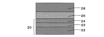
- the organic EL element shown in FIG. 2 includes an anode electrode foil 20 including a metal foil 22, a reflective layer 23, and a buffer layer 24, an organic EL layer 26 provided directly on the buffer layer 24, and an organic EL layer 26. And a cathode 28 as a counter electrode provided directly.
- the buffer layer 24 is preferably composed of a conductive amorphous carbon film or a conductive oxide film so as to be suitable as an anode.
- organic EL layer 26 various known EL layer configurations used for organic EL elements can be used.
- the electron injection layer may be sequentially provided from the anode electrode foil 20 toward the cathode 26.
- layers having various known configurations and compositions can be used as appropriate, and are not particularly limited.
- an organic solar cell can be configured by replacing the organic EL layer 26 with a known organic solar cell active layer.
- a hole transport layer PEDOT: PSS (30 nm)
- a p-type organic semiconductor layer for example, BP (benzoporphyrin) are formed on a buffer layer (for example, a carbon buffer layer).
- An i-type mixing layer of an n-type organic semiconductor and a p-type organic semiconductor for example, BP: PCBNB (fullerene derivative)
- an n-type organic semiconductor layer for example, PCBM (fullerene derivative)
- a buffer layer having a low work function for example, a solar cell can be formed by sequentially laminating Mg—Ag) and a transparent electrode layer (for example, IZO).
- a known material can be appropriately used as a material constituting each of these layers, and is not particularly limited.
- the electrode used for the organic solar cell may have the same material and structure as the electrode used for the organic EL element.
- the electrode foil of the present invention is expected to improve the power generation efficiency due to light confinement due to the cavity effect by providing the reflective layer.
- FIG. 3 shows an example of a layer configuration of a top emission type organic EL lighting in which the organic EL element shown in FIG. 2 is incorporated.
- the organic EL element can be electrically connected to the power source 30 through the metal foil 22 of the anode electrode foil 20.
- a region on the buffer layer 24 that is not in contact with the organic EL layer 26 is covered with an interlayer insulating film 29.
- the interlayer insulating film 29 a Si-based insulating film formed by CVD is preferable because it has a high barrier property against moisture and oxygen that cause deterioration of the organic layer, and more preferably a SiN-based insulating film.
- a more preferred interlayer insulating film is a SiNO insulating film in that the internal stress of the film is small and the flexibility is excellent.
- a sealing material 32 is provided above the cathode 28 so as to face the organic EL element, and a sealing resin 34 is filled between the sealing material 32 and the organic EL element 20 to form a sealing film 34.
- the sealing material 32 glass or a film can be used. In the case of glass, it can be directly bonded onto the sealing film 34 using a hydrophobic adhesive tape. In the case of a film, both surfaces and end surfaces can be covered with a Si-based insulating film. When a film having a high barrier property is developed in the future, it is possible to perform sealing without performing a coating treatment, and it is expected that the film has excellent mass productivity.
- a film is desirable from the viewpoint of imparting flexibility, but a desired performance is obtained by using a sealing material in which a film is bonded to a very thin glass having a thickness of 20 to 100 ⁇ m. It is also possible.
- cathode 28 various known cathodes used for top emission type organic EL elements can be used, and since it is necessary to transmit light, it is not particularly limited as long as it is transparent or translucent. A low one is preferred.
- Preferred cathodes include conductive oxide films, magnesium-based alloy films, and fluoride films, and it is more preferable to combine these in two or more layers. These films can be the same as those described for the buffer layer of the electrode foil.
- a particularly preferable cathode has a two-layer structure in which a transparent oxide layer as a cathode layer made of a conductive oxide film is laminated with a semi-transmissive metal layer as a buffer layer made of a magnesium alloy film and / or a fluoride film.
- a semi-transmissive metal layer as a buffer layer made of a magnesium alloy film and / or a fluoride film.
- the most preferred example is a cathode structure in which a transparent oxide layer (cathode layer) made of IZO (indium zinc oxide) and a semi-transmissive metal layer (buffer layer) made of Mg—Ag are laminated. Further, the cathode structure may include two or more transparent oxide layers and / or two or more semi-transmissive metal layers.
- the light generated in the organic EL layer 26 passes through the cathode 28, the sealing film 34, and the sealing material 32 and is emitted to the outside.
- assistant base material suitably in the back surface of the electrode foil 20 according to a usage form. Since this portion does not affect the light emission characteristics, the degree of freedom in material selection is high. For example, if resin films such as polyethylene terephthalate (PET), polyimide (PI), polycarbonate (PC), polyethersulfone (PES), and polyethernitrile (PEN) are used, the flexibility will not be impaired, so it is optimal. I can say that.
- PET polyethylene terephthalate
- PI polyimide
- PC polycarbonate
- PES polyethersulfone
- PEN polyethernitrile
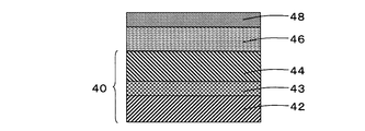
- FIG. 4 shows an example of a layer structure of a top emission type organic EL element using the electrode foil of the present invention as a cathode.
- the organic EL element shown in FIG. 4 includes a cathode electrode foil 40 including a metal foil 42, a reflective layer 43, and a buffer layer 44, an organic EL layer 46 provided directly on the buffer layer 44, and an organic EL layer 46. And an anode 48 as a counter electrode provided directly.
- the organic EL layer 46 can be configured in the same manner as the organic EL layer 26 shown in FIG. 2, and the buffer layer 44 can be configured in the same manner as the cathode 28 shown in FIG. It is preferably composed of a system alloy film, a fluoride film, or a combination of two or more layers thereof.
- a more preferable buffer layer 44 is a semi-transmissive metal layer made of a magnesium-based alloy film and / or a fluoride film.
- the organic EL element using the cathode electrode foil 40 shown in FIG. 4 is the same as the organic EL element using the anode electrode foil 20 shown in FIG. 26 corresponds to a configuration in which the stacking order from the anode side to the cathode side in the interior 26 is reversed.
- a magnesium alloy film or a fluoride film is formed as the buffer layer 44 of the cathode electrode foil 40 by sputtering or vapor deposition, while a conductive amorphous carbon, MoO 3 or V 2 O 5 film is vapor deposited as the anode 48. It is preferable to form by.
- a conductive amorphous carbon film is formed on the organic EL layer, it is preferable to use a vacuum deposition method in order to avoid plasma damage during sputtering.
- Example 1 Preparation of Cu / Al alloy / ITO electrode foil As a metal foil, a commercially available double-sided flat electrolytic copper foil having a thickness of 64 ⁇ m (DFF (Dual Flat Foil) manufactured by Mitsui Metal Mining Co., Ltd.) was prepared.
- DFF Double Flat Foil
- This copper foil was subjected to a CMP (Chemical Mechanical Polishing) process using a polishing machine manufactured by MTT.
- This CMP treatment was performed using a polishing pad with XY grooves and a colloidal silica-based polishing liquid under the conditions of pad rotation speed: 30 rpm, load: 200 gf / cm 2 , and liquid supply amount: 100 cc / min.
- the roughness of the copper foil surface thus treated with CMP was measured in accordance with JIS B 0601-2001 using a scanning probe microscope (Veeco, Nano Scope V). The arithmetic average roughness Ra was 0.7 nm. Met. This measurement was performed by Tapping Mode AFM for a range of 10 ⁇ m square.
- the thickness of the copper foil after the CMP treatment was 48 ⁇ m.
- a 150 nm-thick Al alloy reflective layer was formed on the surface of the CMP-treated copper foil by sputtering.
- This sputtering is performed using a magnetron sputtering apparatus (MSL-) in which an aluminum alloy target (diameter 203.2 mm ⁇ 8 mm thickness) having a composition of Al-0.2B-3.2Ni (at.%) Is connected to a cryo pump. 464, manufactured by Tokki Co., Ltd.), input power (DC): 1000 W (3.1 W / cm 2 ), ultimate vacuum: ⁇ 5 ⁇ 10 ⁇ 5 Pa, sputtering pressure: 0.5 Pa, Ar flow rate: The measurement was performed under the conditions of 100 sccm and substrate temperature: room temperature.
- MSL- magnetron sputtering apparatus
- An ITO buffer layer having a thickness of 10 nm was formed on the surface of the aluminum alloy reflective layer thus obtained by sputtering.
- an ITO (In 2 O 3 —SnO 2 ) target (diameter 203.2 mm ⁇ 6 mm thickness) containing 10% by weight of Sn is connected to a magnetron sputtering apparatus (MSL-464, Tokki) to which a Cryo pump is connected.
- Example 2 Preparation of Cu / Al alloy / C electrode foil An electrode foil was prepared in the same manner as in Example 1 except that a carbon buffer layer having a film thickness of 1.7 nm or 3.5 nm was formed by sputtering instead of the ITO buffer layer. Produced. As a carbon target for this sputtering, an untreated carbon target with a purity of 3N (99.9%) made from a carbon material (IGS743 material, manufactured by Tokai Carbon Co., Ltd.) and a purification treatment with halogen gas on this carbon material. Two types of carbon targets having a purity of 5N (99.999%) were prepared. A carbon buffer layer was formed by sputtering using each of these targets.
- a carbon buffer layer having a film thickness of 1.7 nm or 3.5 nm was formed by sputtering instead of the ITO buffer layer.
- each carbon target (diameter 203.2 mm ⁇ 8 mm thickness) was mounted on a magnetron sputtering apparatus (multi-chamber single-wafer type film forming apparatus MSL-464, manufactured by Tokki Co., Ltd.) connected to a cryo pump.
- ultimate vacuum ⁇ 5 ⁇ 10 ⁇ 5 Pa
- sputtering pressure 0.5 Pa
- Ar flow rate 100 sccm
- substrate temperature room temperature.
- the film thickness was controlled by controlling the discharge time.
- the roughness of the buffer layer surface thus obtained was measured in the same manner as in Example 1, the arithmetic average roughness Ra was 2.45 nm.
- the total thickness of the obtained electrode foil was 48 ⁇ m.
- Example 3 Preparation of Cu / Ag alloy / ITO electrode foil A buffer layer and a reflective layer were provided in the same manner as in Example 1 except that a 150 nm-thick Ag alloy reflective layer was formed by sputtering instead of the Al alloy reflective layer. An electrode foil is prepared.
- a magnetron sputtering apparatus MSL- in which a silver alloy target (diameter 101.6 mm ⁇ 5 mm thickness) having a composition of Ag-1.0Cu-1.0Pd (at.%) Is connected to a Cryo pump.
- Example 4 Production of Organic EL Element An organic EL element having a structure as shown in FIGS. 2 and 3 was produced using the electrode foil (Cu / Al alloy / ITO) produced in Example 1 as an anode.
- a glass substrate (3 cm square ⁇ 0.5 mm thickness) was placed on the electrode foil 20 (5 cm square) for masking, and an interlayer insulating film 29 made of silicon nitride was formed by a plasma CVD (Chemical Vapor Deposition) method.
- This plasma CVD uses a plasma CVD apparatus (PD2202L, manufactured by Samco) connected with a mechanical booster pump (MBP) and a rotary pump (RP).
- the surface of the electrode foil on which the interlayer insulating film was formed was washed as follows. First, in a tank filled with ultrapure water (> 18.0 M ⁇ ), ultrasonic cleaning for 3 minutes was performed twice by replacing ultrapure water. Subsequently, after moisture was removed using nitrogen gas, after-curing was performed at 100 ° C. for 3 hours. The surface thus treated was cleaned by UV irradiation.
- ultrapure water > 18.0 M ⁇
- the organic EL layer 26, the cathode 28, the sealing layer 34, and the sealing material 32 were laminated. Specifically, a 50-nm-thick hole injection layer made of copper phthalocyanine, 4,4′-bis (N, N ′-(3-tolyl) amino) -3,3 ′ is formed on the buffer layer surface of the electrode foil.
- a hole transport layer made of dimethylbiphenyl (HMTPD) with a thickness of 40 nm, a light emitting layer with a thickness of 30 nm formed by doping tris (2-phenylpyridine) iridium complex (Ir (ppy) 3 ) in a host material, Alq3 A 30 nm thick electron transport layer, a 10 nm thick Mg—Ag semi-transmissive film layer (Mg: Ag 9: 1), a 100 nm thick IZO (In—Zn—O) transparent oxide layer, a thickness A 300 nm silicon nitride passivation film (sealing layer), a 2000 nm thick adhesive layer, and a 200 ⁇ m thick sealing glass (sealing material) were laminated in this order.
- HMTPD dimethylbiphenyl
- the sealing glass layer is laminated with a double-sided tape, and this double-sided tape corresponds to the adhesive layer.
- an organic EL element sample having a size of 50 mm square x thickness of 300 ⁇ m and a light emitting area of 30 mm square as shown in FIG. 3 was obtained.
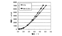
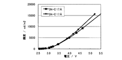
- a voltage of 5.0 V was applied, strong light emission as shown in FIG. 5 could be confirmed.
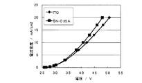
- the change in luminance (cd / m 2 ) and current density (mA / cm 2 ) was measured by changing the applied voltage, the results shown in FIG. 6 and FIG. 7 were obtained (“ITO” in the figure). ”).
- ITO in the figure.
- Example 5 Preparation of organic EL element 3
- the electrode foil (Cu / Al alloy / C) having the following three types of carbon buffer layers prepared in Example 2 was used.
- Various types of organic EL element samples were prepared.
- Sample “3N-C 17 ⁇ ” an organic EL element using a carbon buffer layer having a thickness of 1.7 nm formed using a carbon target having a purity of 3N
- Sample “5N-C 17 ⁇ ” carbon having a purity of 5N
- each of the samples was connected to a power supply 30 as shown in FIG.
- changes in luminance (cd / m 2 ) and / or current density (mA / cm 2 ) were measured by changing the applied voltage, the results shown in FIGS. 6 to 8 were obtained.
- the electrode foil of the present invention when used, light emission with extremely high luminance can be obtained at a low voltage.
- Example 6 Preparation of Cu / Al alloy / Al alloy / ITO electrode foil Example 1 except that an Al alloy reflective layer having a two-layer structure composed of an upper layer and a lower layer was formed by two-stage sputtering through standing in a vacuum. An electrode foil was produced basically in the same manner. In this two-stage sputtering, a lower layer having a thickness of 50 nm is formed on a metal foil under the same conditions as those of the Al alloy reflective layer of Example 1, and the sputtering is temporarily stopped, and the metal foil is vacuum-evacuated as it is in a chamber.
- the film was allowed to stand for about 30 seconds, and sputtering was resumed under the same conditions as described above to form an upper layer having a thickness of 100 nm on the lower layer.
- the overall thickness of the electrode foil thus obtained was 48 ⁇ m.
- the cross section of the electrode foil thus obtained was observed with a transmission electron microscope (TEM), the micrograph shown in FIG. 10 was obtained.
- the reflective layer has a laminated structure composed of two layers separated by an interface that appears to be amorphous with a thickness of about 1 nm, and the two layers have different crystal orientations ( It was observed that the lower layer has a generally horizontal direction and the upper layer has a generally vertical direction.
- Example 7 Preparation of Cu / Al alloy / Al alloy / ITO electrode foil Example 1 except that an Al alloy reflective layer having a two-layer structure consisting of an upper layer and a lower layer was formed by two-step sputtering through standing in the atmosphere. Similarly, an electrode foil was produced. In this two-stage sputtering, a lower layer having a thickness of 50 nm is formed on the metal foil under the same conditions as those of the Al alloy reflective layer of Example 1, and the sputtering is temporarily stopped, and the metal foil is taken out of the chamber into the atmosphere.
- the metal foil was returned to the chamber again for about 30 seconds, and sputtering was resumed under the same conditions as described above to form an upper layer having a thickness of 100 nm on the lower layer.
- the overall thickness of the electrode foil thus obtained was 48 ⁇ m.
- the cross section of the electrode foil thus obtained was observed with a TEM, the micrograph shown in FIG. 12 was obtained.
- the reflective layer had a laminated structure composed of two layers separated by an interface, and the two layers had different crystal orientations with the interface as a boundary.
- EDX analysis was performed on the interface of the obtained reflective layer, a spectrum having peaks derived from Al and O as shown in FIG. 13 was obtained.
- the oxygen component was detected from the interface, it is understood that the natural oxide film constitutes the interface.
- Example 8 Preparation of Cu / Al Alloy Electrode Foil
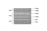
- an Al alloy reflective layer 143 with a film thickness of 150 nm was formed by sputtering on a copper foil 142 manufactured under the same conditions as in Example 1. .
- This sputtering is performed using a magnetron sputtering apparatus (MSL-464, manufactured by Tokki Co., Ltd.) in which an aluminum alloy target (diameter 203.2 nm ⁇ 8 mm thickness) having a composition of Al-4Mg (at.%) Is connected to a Cryo pump.
- MSL-464 magnetron sputtering apparatus
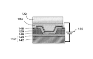
- Example 9 Production of Organic EL Device Using the electrode foil 140 (Cu / Al alloy) produced in Example 8 as a cathode, an organic EL device having a structure as shown in FIGS. 14 and 15 was produced. First, a glass substrate (3 cm square ⁇ 0.5 mm thickness) was placed on the electrode foil 140 (5 cm square) for masking, and an interlayer insulating film 29 made of silicon nitride was formed by a plasma CVD (Chemical Vapor Deposition) method. This plasma CVD uses a plasma CVD apparatus (PD2202L, manufactured by Samco) connected with a mechanical booster pump (MBP) and a rotary pump (RP).
- P2202L plasma CVD apparatus
- MBP mechanical booster pump
- RP rotary pump
- the organic EL layer 146, the anode 148, the sealing layer 134, and the sealing material 132 were laminated on the electrode foil thus cleaned.
- an ⁇ -NPD layer 146b with a thickness of 50 nm, an Alq3 layer 146a with a thickness of 50 nm, a MoO 3 layer 148b with a thickness of 20 nm, an IZO (In—Zn) with a thickness of 100 nm are formed on the surface of the reflective layer 143 of the electrode foil.
- a transparent oxide layer 148a, a 300 nm thick silicon nitride passivation film (sealing layer 134), a 2000 nm thick adhesive layer, and a 200 ⁇ m thick sealing glass (sealing material 132) were laminated in this order.
- the sealing glass layer is laminated with a double-sided tape, and this double-sided tape corresponds to the adhesive layer.
- an organic EL element sample having a size of 50 mm square x thickness of 300 ⁇ m and a light emitting area of 30 mm square as shown in FIG. 15 was obtained. When this sample was connected to the power supply 130 and a voltage of 10 V was applied, green light emission caused by Alq3 could be confirmed.
Landscapes
- Physics & Mathematics (AREA)
- Optics & Photonics (AREA)
- Electromagnetism (AREA)
- Electroluminescent Light Sources (AREA)
- Photovoltaic Devices (AREA)
- Physical Vapour Deposition (AREA)
Abstract
支持基材および反射電極としての機能を兼ね備え、かつ、熱伝導性に優れた、電極箔ならびにそれを用いた有機デバイスが提供される。この電極箔は、金属箔と、金属箔上に直接設けられる反射層とを備えてなる。
Description
この出願は、2010年6月4日に出願された日本国特許出願第2010-129064号および2010年8月4日に出願された日本国特許出願第2010-175420号に基づく優先権を主張するものであり、それらの全体の開示内容が参照により本明細書に組み込まれる。
本発明は、金属箔を用いた電極箔、ならびに電極箔を用いた有機EL素子、有機EL照明、有機太陽電池等の有機デバイスに関する。
近年、有機EL照明が、環境に配慮したグリーンデバイスとして注目されている。有機EL照明の特徴としては、1)白熱灯に対して低消費電力であること、2)薄型かつ軽量であること、3)フレキシブルであることが挙げられる。現在、有機EL照明は、上記2)および3)の特徴を実現すべく開発が進められている。この点、フラットパネルディスプレイ(FPD)等で従来使用されてきたガラス基板では、上記2)および3)の特徴を実現することは不可能である。
そこで、有機EL照明のための支持体としての基板(以下、支持基材という)に対する研究が進められており、その候補として、極薄ガラス、樹脂フィルム、金属箔等が提案されている。極薄ガラスは、耐熱性、バリア性、および光透過性に優れ、フレキシブル性も良好であるが、ハンドリング性がやや劣り、熱伝導性が低く、材料コストも高い。また、樹脂フィルムは、ハンドリング性およびフレキシブル性に優れ、材料コストも低く、光透過性も良好であるが、耐熱性およびバリア性に乏しく、熱伝導性が低い。
これに対し、金属箔は、光透過性が無いことを除けば、耐熱性、バリア性、ハンドリング性、熱伝導性に優れ、フレキシブル性も良好であり、材料コストも低いといった優れた特徴を有する。特に、熱伝導性については、典型的なフレキシブルガラスやフィルムが1W/m℃以下と極めて低いのに対し、銅箔の場合、280W/m℃程度と極めて高い。ただし、金属箔をフレキシブル電子デバイスの支持基材として用いるためには、その表面を絶縁膜で被覆することが必要とされている。
例えば、特許文献1には、フレキシブル基板上に、下部電極層、有機層および上部電極層を備えた有機発光デバイスが開示されており、フレキシブル基板として、絶縁層で被覆してもよい金属箔を使用できることが記載されている。
特許文献2には、表面粗さRaが30nm以上500nm以下のステンレス箔を備えた、フレキシブルな電子デバイス用絶縁被覆金属箔が開示されている。この金属箔は、表面に絶縁膜が被覆されることで、薄膜トランジスタ(TFT)等の電子デバイスが形成されるための支持基材として用いられる。
特許文献3には、表面粗さRaが0.2μm以下程度の金属箔表面に熱圧着性ポリイミド塗膜が積層されたフレキシブル金属箔積層体が開示されている。
特許文献4には、絶縁層構成材料との張り合わせ面の低プロファイル化を図るべく、析出面側の表面粗さ(Rzjis)を1.0μm未満とした電解銅箔が開示されているが、この文献に開示される表面粗さ(Rzjis)は最も平坦なものでもせいぜい0.27μmである。
本発明者は、今般、反射層を金属箔上に直接設けることで、支持基材および反射電極としての機能を兼ね備え、かつ、熱伝導性に優れた、フレキシブル電子デバイスに有用な電極箔が得られるとの知見を得た。
したがって、本発明の目的は、支持基材および反射電極としての機能を兼ね備え、かつ、熱伝導性に優れた、フレキシブル電子デバイスに有用な電極箔を提供することにある。
本発明の一態様によれば、金属箔と、前記金属箔上に直接設けられる反射層とを備えてなる電極箔が提供される。
本発明の別の態様によれば、上記電極箔と、
前記電極箔の前記反射層側の最表面に直接設けられる有機EL層および/または有機太陽電池活性層からなる有機半導体層と、
前記有機半導体層上に設けられる、透明又は半透明の対向電極と、
を備えた、有機EL素子および/または有機太陽電池である、有機デバイスが提供される。
前記電極箔の前記反射層側の最表面に直接設けられる有機EL層および/または有機太陽電池活性層からなる有機半導体層と、
前記有機半導体層上に設けられる、透明又は半透明の対向電極と、
を備えた、有機EL素子および/または有機太陽電池である、有機デバイスが提供される。
本発明にさらに別の態様によれば、上記有機デバイスを有機EL素子として備えてなる、有機EL照明が提供される。
電極箔
図1に本発明による電極箔の一例の模式断面図を示す。図1に示される電極箔10は、金属箔12、金属箔上に直接設けられる反射層13、および所望により反射層上に直接設けられるバッファ層14を備えてなる。すなわち、電極箔10は金属箔12、反射層13およびバッファ層14を備えた3層構成であるが、本発明の電極箔はこれに限定されず、金属箔12および反射層13の2層構成であってもよい。トップエミッション型有機EL素子において金属電極層上に反射層を形成することは一般的に行われているが、この金属電極層は絶縁基板等の支持基材上に形成されなければならないものと信じられてきた。事実、本発明者の知るかぎり、それ自体単独でハンドリングが可能な金属箔に反射層を形成して有機EL素子のアノードまたはカソードとして使用しようとする試みは今までなされていない。本発明にあっては、金属箔12を支持基材のみならず電極として用い、かつ、その上に反射層13を直接設けることで、支持基材、電極および反射層の3つの機能を兼ね備えた従来に無い電極箔を提供することができる。したがって、本発明の電極箔によれば、従来のトップエミッション型フレキシブル発光デバイスで必要とされてきた支持基材および反射層を不要にすることができる。このため、本発明の電極箔は、少なくとも反射層側に絶縁層を有しないものであり、好ましくはいかなる部位にも絶縁層を有しない。
図1に本発明による電極箔の一例の模式断面図を示す。図1に示される電極箔10は、金属箔12、金属箔上に直接設けられる反射層13、および所望により反射層上に直接設けられるバッファ層14を備えてなる。すなわち、電極箔10は金属箔12、反射層13およびバッファ層14を備えた3層構成であるが、本発明の電極箔はこれに限定されず、金属箔12および反射層13の2層構成であってもよい。トップエミッション型有機EL素子において金属電極層上に反射層を形成することは一般的に行われているが、この金属電極層は絶縁基板等の支持基材上に形成されなければならないものと信じられてきた。事実、本発明者の知るかぎり、それ自体単独でハンドリングが可能な金属箔に反射層を形成して有機EL素子のアノードまたはカソードとして使用しようとする試みは今までなされていない。本発明にあっては、金属箔12を支持基材のみならず電極として用い、かつ、その上に反射層13を直接設けることで、支持基材、電極および反射層の3つの機能を兼ね備えた従来に無い電極箔を提供することができる。したがって、本発明の電極箔によれば、従来のトップエミッション型フレキシブル発光デバイスで必要とされてきた支持基材および反射層を不要にすることができる。このため、本発明の電極箔は、少なくとも反射層側に絶縁層を有しないものであり、好ましくはいかなる部位にも絶縁層を有しない。
金属箔12は、支持基材としての強度および電極として必要な電気的特性を有する箔状金属材料であれば特に限定されない。好ましい金属箔は、加工時に発生する粒子状物の帯磁による付着を防止できる観点から、非磁性金属箔である。非磁性金属の好ましい例としては、銅、アルミニウム、非磁性ステンレス、チタン、タンタル、モリブデン等が挙げられ、より好ましくは銅、アルミニウム、および非磁性ステンレスである。最も好ましい金属箔は銅箔である。銅箔は比較的安価でありながら、強度、フレキシブル性、電気的特性等に優れる。
電極箔10の少なくとも一方の最表面は、10.0nm以下の算術平均粗さRaを有する超平坦面とするのが好ましく、より好ましくは7.0nm以下、さらに好ましくは5.0nm、さらにより好ましくは3.0nm以下、特に好ましくは2.8nm以下、特により好ましくは2.5nm以下、最も好ましくは2.0nm以下である。算術平均粗さRaの下限は特に限定されずゼロであってもよいが、平坦化処理の効率を考慮すると0.5nmが下限値の目安として挙げられる。この算術平均粗さRaは、JIS B 0601-2001に準拠して市販の粗さ測定装置を用いて測定することができる。
ここで、電極箔10の少なくとも一方の最表面とは、2層構成の場合には反射層13の表面13aを、3層構成の場合にはバッファ層14の表面14aを意味する。もっとも、2層構成の場合において反射層13の表面13aにおける上記算術平均粗さRaの実現は、反射層13が形成されることになる金属箔12の表面12aの算術平均粗さRaを上記同様の範囲、すなわち10.0nm以下、好ましくは6.0nm以下、より好ましくは3.0nm以下、さらに好ましくは2.0nm以下、さらにより好ましくは1.5nm以下にしておき、その上にバッファ層14を成膜することにより行うことができる。3層構成の場合におけるバッファ層14の表面14aにおける上記算術平均粗さRaの実現は、上記のようにして10.0nm以下、好ましくは6.5nm以下、より好ましくは3.0nm以下、さらに好ましくは2.5nm以下、さらにより好ましくは2.0nm以下の算術平均粗さRaが付与された反射層13の上にバッファ層14を成膜することにより行うことができる。こうして形成されたバッファ層14の表面14aは、10.0nm以下、好ましくは7.0nm以下、より好ましくは5.0nm、さらにより好ましくは3.0nm以下、特に好ましくは2.8nm以下、特により好ましくは2.5nm以下の算術平均粗さRaを有する。このように、最表面において付与されるべき算術平均粗さRaよりも同等もしくは若干小さめの算術平均粗さRaをそれよりも下の層ないし箔の表面に付与しておくのが好ましい。なお、積層状態のため最表面を構成しない金属箔表面の算術平均粗さRaの評価は、金属箔表面からFIB(Focused Ion Beam)加工にて断面を作製し、その断面を透過型電子顕微鏡(TEM)にて観察することにより行うことができ、積層状態のため最表面を構成しない反射層表面の算術平均粗さRaの評価も同様にして行うことができる。
本発明者の知るかぎり、このような超平坦表面を有する金属箔(特に銅箔)は今まで工業的に製造されておらず、ましてやそれをフレキシブル電子デバイスの電極そのものとして応用しようとする試みは今までなされていなかった。表面を平坦化した銅箔は市販されているが、このような銅箔の平坦化レベルは有機EL素子用電極としては不十分なものであり、有機EL素子とした場合に表面の凹凸により短絡を起こしてしまい、発光が得られないおそれがある。
これに対し、金属箔12の超平坦面12aの算術平均粗さRaが上述のごとく極めて小さいと、有機EL素子用電極として用いても対向電極等との間で起こりうる短絡を効果的に防止できる。このような超平坦面は、CMP(Chemical Mechanical Polishing)処理により金属箔を研磨することにより実現することができる。CMP処理は、公知の研磨液および公知の研磨パッドを用いて、公知の条件に従って行うことができる。好ましい研磨液としては、セリア、シリカ、アルミナ、ジルコニア等から選択される1種以上の研磨砥粒約0.5~2重量%程度を含んでなり、かつ、ベンゾトリアゾール(BTA)等の酸化剤と、さらに/または、キナルシン酸、キノリン酸、ニコチン酸等の有機錯体形成剤と、カチオン性界面活性剤、アニオン性界面活性剤等の界面活性剤と、所望により防食剤とをさらに含むものが挙げられる。好ましい研磨パッドとしては、ウレタン製のパッドが挙げられる。研磨条件は、パッド回転速度、ワーク荷重、研磨液塗布流量等を適宜調整すればよく特に限定されないが、回転速度を20~1000rpmの範囲内に、ワーク荷重を100~500gf/cm2の範囲内に、研磨液塗布流量を20~200cc/min範囲内に調整するのが好ましい。
超平坦面12aは、電解研磨法、バフ研磨法、薬液研磨法、およびこれらの組み合わせ等を用いて金属箔12を研磨することによっても実現することができる。薬液研磨法は、薬液、薬液温度、薬液浸漬時間等を適宜調整して行えばよく特に限定されないが、例えば、銅箔の薬液研磨は、2-アミノエタノールと塩化アンモニウムとの混合物を使用することにより行うことができる。薬液温度は室温が好ましく、浸漬法(Dip法)を用いるのが好ましい。また、薬液浸漬時間は、長くなると平坦性が悪化する傾向があるため、10~120秒間が好ましく、30~90秒間がより好ましい。薬液研磨後の金属箔は流水により洗浄されるのが好ましい。このような平坦化処理によれば、Ra算術平均粗さRa12nm程度の表面をRa10.0nm以下、例えば3.0nm程度にまで平坦化することができる。
超平坦面12aは、金属箔12の表面をブラストにより研磨する方法や、金属箔12の表面をレーザー、抵抗加熱、ランプ加熱等の手法により溶融させた後に急冷させる方法等によっても実現することもできる。また、金属箔12として、銅、ニッケル、クロムのようにメッキが可能な金属箔を用いた場合には、転写法を用いて超平坦面を実現することもできる。転写法は、公知の手法及び公知の条件に基づいて行えばよい。例えば、電解研磨法及びバフ研磨法を用いて、SUS、チタン等の電極板の表面を算術平均粗さRaが10.0nm以下、例えば3.0nm以下になるよう平坦化しておく。この平坦化された電極板の表面に金属箔12の材料をめっきし、所望の厚さに達した時点で金属箔12の材料を電極板より剥離する。こうして金属箔12の剥離面に電極板表面の平坦性を転写させることで、超平坦面を実現することができる。
金属箔12の厚さは、フレキシブル性を損なうことなく、箔として単独でハンドリングが可能な厚さである限り特に限定されないが、1~250μm、好ましくは25~250μm、より好ましくは35~150μmである。このような厚さであれば、市販の裁断機を用いて簡単に切断することが可能である。また、金属箔12は、ガラス基板と異なり、割れ、欠け等の問題が無く、また、切断時のパーティクルが発生しづらい等の利点も有する。金属箔12は、四角形以外の形状、例えば、円形、三角形、多角形といった様々な形状とすることができ、しかも切断および溶接も可能なことから、切り貼りによりキュービック状やボール状といった立体的な形状の発光体を作製することも可能である。この場合、金属箔12の切断部や溶接部には、発光層を形成しないことが好ましい。
超平坦面12aはアルカリ溶液で洗浄することが好ましい。そのようなアルカリ溶液としては、アンモニアを含有した溶液、水酸化ナトリウム溶液、水酸化カリウム溶液等の公知のアルカリ溶液が使用可能である。好ましいアルカリ溶液はアンモニアを含有した溶液であり、より好ましくはアンモニアを含有した有機系アルカリ溶液、さらに好ましくはテトラメチルアンモニウムハイドロオキサイド(TMAH)溶液である。TMAH溶液の好ましい濃度は0.1~3.0wt%である。そのような洗浄の一例としては、0.4%TMAH溶液を用いて23℃で1分間の洗浄を行うことが挙げられる。このようなアルカリ溶液による洗浄と併せて、または、アルカリ溶液による洗浄の代わりに、UV(Ultra Violet)処理を行っても同様の洗浄効果を得ることができる。さらに、銅箔等の場合、希硫酸等の酸性洗浄液を用いて、銅表面に形成されうる酸化物を除去することも可能である。
酸洗浄の一例としては、希硫酸を用いて30秒間の洗浄を行うことが挙げられる。
酸洗浄の一例としては、希硫酸を用いて30秒間の洗浄を行うことが挙げられる。
反射層13の成膜前に、超平坦面12a上に存在するパーティクルを除去することが好ましい。有効なパーティクル除去の手法としては、超純水によるソニック洗浄法やドライアイスブラスト法等が挙げられるが、ドライアイスブラスト法がより効果的である。ドライアイスブラスト法は、高圧に圧縮した炭酸ガスを細いノズルから噴射させることにより、低温固化した炭酸を超平坦面12aに吹き付けてパーティクルを除去する方法である。
このドライアイスブラスト法は、ウェット工程とは異なり、乾燥工程を省くことができ、また有機物の除去ができる等の利点を有する。ドライアイスブラスト法は、例えばドライアイススノーシステム(エアウォーター社製)等の市販の装置を用いて行うことができる。
このドライアイスブラスト法は、ウェット工程とは異なり、乾燥工程を省くことができ、また有機物の除去ができる等の利点を有する。ドライアイスブラスト法は、例えばドライアイススノーシステム(エアウォーター社製)等の市販の装置を用いて行うことができる。
金属箔12の超平坦面上には反射層13が直接設けられる。反射層13は、アルミニウム、アルミニウム系合金、銀、および銀系合金からなる群から選択される少なくとも一種で構成されるのが好ましい。これらの材料は、光の反射率が高いため反射層に適しており、しかも薄膜化した際の平坦性にも優れる。特に、アルミニウムまたはアルミニウム系合金は安価な材料であることから好ましい。アルミニウム系合金および銀系合金としては、有機EL素子等の表示デバイスにおいてアノードまたはカソードとして使用される一般的な合金組成を有するものが幅広く採用可能である。好ましいアルミニウム系合金組成の例としては、Al-Ni、Al-Cu、Al-Ag、Al-Ce、Al-Zn、Al-B、Al-Ta、Al-Nd、Al-Si、Al-La、Al-Co、Al-Ge、Al-Fe、Al-Li、Al-Mg、Al-Mn合金が挙げられる。これらの合金を構成する元素であれば、必要な特性に合わせて任意に組み合わせることが可能である。また、好ましい銀合金組成の例としては、Ag-Pd、Ag-Cu、Ag-Al、Ag-Zn、Ag-Mg、Ag-Mn、Ag-Cr、Ag-Ti、Ag-Ta、Ag-Co、Ag-Si、Ag-Ge、Ag-Li、Ag-B、Ag-Pt、Ag-Fe、Ag-Nd、Ag-La、Ag-Ce合金が挙げられる。これらの合金を構成する元素であれば、必要な特性に合わせて任意に組み合わせることが可能である。反射層13の膜厚は特に限定されるものではないが、30~500nmの厚さを有するのが好ましく、より好ましくは50~300nmであり、さらに好ましくは100~250nmである。
反射層13の表面13aは好ましくは10.0nm以下、より好ましくは6.5nm以下、さらに好ましくは3.0nm以下、さらにより好ましくは2.5nm以下、特に好ましくは2.0nm以下の算術平均粗さRaを有する。前述のとおり、本発明の電極箔においては超平坦な金属箔表面に反射層が形成されるため、反射層の表面においても算術平均粗さRaを小さくして高い平坦性を実現できる。これにより、過度な凹凸の発生に起因する有機EL層間における短絡のリスクを低減することができる。また、反射層表面の凹凸による影響を排除すべく正孔注入層および正孔輸送層あるいは電子注入層および電子輸送層を厚く設ける必要がないので、これらの層ならびにそれらを含む有機EL層を従来以上に薄くすることができる。その結果、極めて高価な有機原料の使用量を減らして製造コストを低減するとともに、有機EL層の薄膜化により発光効率を向上することができる。
反射層13がアルミニウム膜またはアルミニウム系合金膜で構成される場合、図9に示されるように反射層を少なくとも2つの層からなる積層構造で構成してもよい。すなわち、図9に示される電極箔50は、図1に示される電極箔10と同様、金属箔52、反射層53および所望によるバッファ層54を有するが、反射層53が界面53cによって仕切られた2つの層53a,53bの積層構造を有し、この界面53cを境に下層53aおよび上層53bが互いに異なる結晶方位を有する。これにより、電極箔がかなりの高温に曝される場合であっても、銅箔とアルミニウム含有反射層の間の界面から起こりうるサーマルマイグレーションを効果的に抑制して、サーマルマイグレーションに起因する表面平坦性や反射率の低下を抑制することができる。すなわち、電極箔の耐熱性を向上することができる。したがって、この態様は、200℃以上、好ましくは230℃以上、より好ましくは250℃以上の温度で行われる、正孔注入層塗布後の熱処理において特に有効であるといえる。このような耐熱性の向上は、結晶粒界を優先して進行するサーマルマイグレーションが、結晶粒界が不連続となる界面53cによって阻止されることにより実現されるものと考えられる。なお、反射層53中の界面53cの数は2つ以上であってもよく、この場合、反射層は3層以上の積層構造となる。
積層構造の反射層53は、スパッタリング等の成膜プロセスを、所定のインターバルを経て複数回行うことにより作製することができる。そのような方法の好ましい例としては以下のものが挙げられる。
(1)スパッタリング法により下層53aの成膜を好ましくは厚さが10nm以上になるまで行い、スパッタリングを一時的に停止する。この状態で下層53aをスパッタリング装置のチャンバ内に放置する。この放置時間は30秒以上とすることが好ましい。次いで、スパッタリングを再開して上層53bの成膜を行う。
(2)スパッタリング法により下層53aの成膜を好ましくは厚さが10nm以上になるまで行い、スパッタリングを一時的に停止する。そして、下層53aを大気に接触させる。この大気接触は、下層53aが形成された金属箔をスパッタリング装置のチャンバから取り出して大気に曝してもよいし、金属箔を取り出すことなくチャンバを大気に解放してもよい。次いで、スパッタリングを再開して上層53bの成膜を行う。下層53aを大気に曝す時間は数秒程度で十分であり、通常のクリーンルーム環境におけるような湿度および温度で所望の効果が得られる。
(3)スパッタリング法により下層53aの成膜を好ましくは厚さが10nm以上になるまで行い、スパッタリングを一時的に停止する。次いで、スパッタリング装置のチャンバ内に酸素を導入して酸素雰囲気にした後、再度真空引きして上層53bの成膜を行う。酸素を導入したチャンバ内の圧力は0.01Pa以上であるのが好ましく、より好ましくは0.1Pa以上、さらに好ましくは1Pa以上である。
積層構造の反射層53において、界面53cの数は一つで十分である。一つの界面であっても250℃程度という高温下で十分な耐熱性を発揮する。もっとも、成膜プロセスの回数を増やして界面を2つ以上に設けることにより、更なる耐熱性の向上を図ってもよい。
反射層13上にはバッファ層14が直接設けられるのが好ましい。バッファ層14は、有機EL素子において有機EL層と接触して正孔注入効率または電子注入効率を向上させ、所望の仕事関数を与えるものであれば特に限定されない。もっとも、本発明におけるバッファ層は、金属箔を反射層として機能させる観点から、透明または半透明であるのが好ましい。
バッファ層14は、導電性非晶質炭素膜、導電性酸化物膜、マグネシウム系合金膜、およびフッ化物膜から選択される少なくとも一種であるのが好ましく、アノードまたはカソードといった適用用途および要求される特性に応じて適宜選択すればよい。
導電性非晶質炭素膜としては、水素濃度や不純物濃度を制御することにより導電性が付与された種々の非晶質炭素膜が使用可能である。導電性非晶質炭素膜の形成はスパッタリング法によって行われるのが好ましい。スパッタリングに用いるカーボンターゲットとしては、純化処理を施した物を使用することが望ましい。また、多孔質のカーボンに、B、Si、Al、Cuを含浸させたものを使用することも可能である。導電性非晶質炭素膜をバッファ層として用いる場合には、反射層として、アルミニウム膜、アルミニウム系合金膜、銀膜、および銀系合金膜のいずれも適するが、平坦性および材料コストを考慮するとアルミニウム合金が好ましい。
好ましい導電性非晶質炭素膜は、水素濃度が15at%以下である導電性非晶質炭素で構成される。より好ましい水素濃度は12at%以下であり、さらに好ましくは5at%以下である。なお、水素濃度の下限は特に限定されずゼロであってもよいが、スパッタリング時の成膜環境等に起因する水素の不可避的混入を考慮すると3at%が下限値の目安として挙げられる。なお、バッファ層中の水素濃度の測定は公知の各種方法により行うことができるが、HFS(水素前方散乱:Hydrogen Forward Scattering)により行われるのが好ましい。本明細書において、導電性非晶質炭素膜中の水素濃度は、HFS等で炭素および水素を定量し、これらの原子数の合計を100at%としたときの水素濃度として定義される。このように水素濃度を極めて低くすることにより、バッファ層を構成する炭素が水素で終端されることによる導電性の低下ないし絶縁性の発現を回避して、電極としての高い導電性をバッファ層に持たせることができる。したがって、導電性非晶質炭素には炭素および水素以外の不純物が実質的にドープされていないのが好ましい。ここで「実質的にドープされていない」とは何らかの機能を付与するために不純物が意図的にドープされていないとの意味であり、スパッタリング時の成膜環境等に起因して不可避的に混入される不純物は許容される。このような観点から、本発明において導電性非晶質炭素は、0~300wtppmの酸素濃度、0~1000wtppmのハロゲン元素濃度、0~500wtppmの窒素濃度を有するのが好ましい。バッファ層14の膜厚は特に限定されないが3~30nmであるのが好ましく、より好ましくは3~15nmであり、さらに好ましくは5~10nmである。
好ましい導電性酸化物膜としてはInOx、SnOx、ZnOx、MoOx、GaOx、VOx、WOx、RuOx、AlOx、TiOx、およびGeOxからなる群から選ばれる1種または2種以上で構成される膜が挙げられ、典型例としてはITO(インジウム錫酸化物)やIZO(インジウム亜鉛酸化物)が挙げられる。導電性酸化物膜の形成は、スパッタリング法、真空蒸着法等の公知の手法によって行えばよく、好ましくはDCマグネトロンスパッタリング法により行われる。スパッタリング法に用いられるターゲット材は、ホットプレス法やコールドプレス法により作製可能であるため、上記酸化物を適宜組み合わせて所望の特性が得られるようにすることが可能である。導電性酸化物膜をバッファ層として用いる場合には、反射層としては、Al-Ni系合金、Ag、またはAg系合金が特に適する。
好ましいマグネシウム系合金膜としては、MgにAg、Al、Zn、Li、YおよびCaから選択される1種以上が添加された合金で構成される膜が挙げられる。マグネシウム系合金膜の形成はスパッタリング法、真空蒸着法等の公知の手法によって行えばよく、好ましくは真空蒸着法により行われる。
好ましいフッ化物膜としては、LiF、MgF2、CaF2、AlF3、Na3AlF6およびNaF6から選択される1種以上で構成される膜が挙げられる。フッ化物膜の形成はスパッタリング法、真空蒸着法等の公知の手法によって行えばよく、好ましくは真空蒸着法により行われる。
バッファ層14の表面14aは好ましくは10.0nm以下、より好ましくは7.0nm以下、さらに好ましくは5.0nm、さらにより好ましくは3.0nm以下、特に好ましくは2.8nm以下、特により好ましくは2.5nm以下の算術平均粗さRaを有する。前述のとおり、本発明の電極箔においては超平坦な金属箔に起因する超平坦な反射膜表面にバッファ層が形成されるため、バッファ層の表面においても算術平均粗さRaを小さくして高い平坦性を実現できる。これにより、過度な凹凸の発生に起因する有機EL層間における短絡のリスクを低減することができる。また、バッファ層表面の凹凸による影響を排除すべく正孔注入層および正孔輸送層あるいは電子注入層および電子輸送層を厚く設ける必要がないので、これらの層ならびにそれらを含む有機EL層を従来以上に薄くすることができる。その結果、極めて高価な有機原料の使用量を減らして製造コストを低減するとともに、有機EL層の薄膜化により発光効率を向上することができる。
反射層13とバッファ層14との間には酸化膜(図示せず)が存在していてもよい。この酸化膜は、典型的にはアノード層が雰囲気中の酸素によって不可避的に酸化されることにより形成されることがある。このような酸化膜はできるだけ薄い方が好ましく、好ましい厚さは3.0nm以下であり、より好ましくは1.5nm以下である。このような酸化膜はエッチング等により除去してもよい。
本発明による電極箔は、1~300μmの厚さを有するのが好ましく、より好ましくは25~250μm、さらに好ましくは35~150μm、最も好ましくは40~100μmの厚さを有する。
本発明の好ましい態様によれば、金属箔12の反射層13と反対側の表面12bが、1.0μm以上、より好ましくは2.0μm以上、さらに好ましくは5.0μm以上の十点平均粗さRzを有する粗化面となるように加工してもよい。この十点平均粗さRzは、JIS B 0601-1994に準拠して市販の粗さ測定装置を用いて測定することができる。この表面を粗くする加工は、ドライアイスブラスト、サンドブラスト、ウェットエッチング、ドライエッチング等の公知の手法により好ましく行うことができる。この粗化面の表面に形成された凹凸により放熱特性を向上させることができる。
本発明による電極箔は、金属箔をベースとしているため、支持基材を特に必要とすることなく、例えばロール・トゥ・ロール(roll-to-roll)プロセスによって効率的に製造することができる。
本発明による電極箔は、各種フレキシブル電子デバイス用(特にフレキシブル発光または発電デバイス)のアノードまたはカソードとして好ましく用いることができ、それにより反射電極として機能することができる。そのようなフレキシブル電子デバイスの例としては、有機EL素子、有機EL照明、有機ELディスプレイ、電子ペーパー、薄膜太陽電池、液晶ディスプレイ、無機EL素子、無機ELディスプレイ、LED照明、LEDディスプレイが挙げられるが、好ましくは有機EL素子、有機EL照明、有機ELディスプレイ、有機太陽電池、色素増感太陽電池であり、より好ましくは極薄で高輝度の発光が得られる点で有機EL照明である。また、有機太陽電池の場合、電極材料に求められる特性の多くが有機EL素子の場合に求められる特性と共通するため、本発明による電極箔は有機太陽電池のアノードまたはカソードとして好ましく用いることができる。すなわち、本発明による電極箔上に積層させる有機半導体層の種類を公知の技術に従い適宜選択することにより、有機デバイスを有機EL素子および有機太陽電池のいずれにも構成することが可能となる。また、同一電極上に発光素子および発電素子を同時に形成することも可能となり、それによって有機EL素子の機能と有機太陽電池の機能を併せ持った複合デバイスを作製することもできる。さらに、本発明による電極箔は、有機EL素子の電極のみならず、LEDの実装基板にも使用することができる。特に、本発明による電極箔は、LED素子を密に実装することができる点でLED照明用のアノードまたはカソードとして好ましく用いることができる。
有機EL素子および有機EL照明
本発明による電極箔を反射電極として用いて、トップエミッション型有機EL素子および有機EL照明を構築することができる。
本発明による電極箔を反射電極として用いて、トップエミッション型有機EL素子および有機EL照明を構築することができる。
図2に、本発明の電極箔をアノードとして用いたトップエミッション型有機EL素子の層構成の一例を示す。図2に示される有機EL素子は、金属箔22、反射層23およびバッファ層24を備えたアノード電極箔20と、バッファ層24上に直接設けられる有機EL層26と、有機EL層26上に直接設けられる対向電極としてのカソード28とを備えてなる。バッファ層24は、アノードとして適するように導電性非晶質炭素膜または導電性酸化物膜で構成されるのが好ましい。
有機EL層26としては、有機EL素子に使用される公知の種々のEL層構成が使用可能であり、所望により正孔注入層および/または正孔輸送層、発光層、ならびに所望により電子輸送層および/または電子注入層を、アノード電極箔20からカソード26に向かって順次備えてなることができる。正孔注入層、正孔輸送層、発光層、電子輸送層、および電子注入層としては、それぞれ公知の種々の構成ないし組成の層が適宜使用可能であり特に限定されるものではない。
前述のように、有機EL層26を公知の有機太陽電池活性層で置き換えることにより、有機太陽電池を構成することができる。本発明の電極箔をアノードとして用いる有機太陽電池の場合、バッファ層(例えばカーボンバッファ層)上に、正孔輸送層(PEDOT:PSS(30nm))、p型有機半導体層(例えばBP(ベンゾポルフィリン))、n型有機半導体とp型有機半導体のi型ミキシング層(例えばBP:PCBNB(フラーレン誘導体))、n型有機半導体層(例えばPCBM(フラーレン誘導体))、低い仕事関数を有するバッファ層(例えばMg-Ag)および透明電極層(例えばIZO)を順次積層させて太陽電池を構成することが可能である。これらの各層を構成する材料としては公知の材料を適宜使用することができ、特に限定されない。有機太陽電池に使用される電極は、有機EL素子に使用される電極と同じ材料および構造を有するものであってよい。本発明の電極箔は反射層を備えることで、キャビティー効果に起因する光の閉じ込めによる発電効率の向上が期待される。
図3に、図2に示される有機EL素子が組み込まれたトップエミッション型有機EL照明の層構成の一例が示される。図3に示される有機EL照明において、有機EL素子はアノード電極箔20の金属箔22を介して電源30に電気的に接続可能とされる。バッファ層24上の、有機EL層26と非接触の領域は層間絶縁膜29で被覆される。層間絶縁膜29としては、CVD成膜したSi系絶縁膜が、有機層を劣化させる原因となる水分および酸素に対するバリア性が高いことから好ましく、より好ましくはSiN系絶縁膜である。さらに好ましい層間絶縁膜は、膜の内部応力が小さく、屈曲性に優れる点で、SiNO系絶縁膜である。
カソード28の上方には有機EL素子と対向して封止材32が設けられ、封止材32と有機EL素子20との間には封止用樹脂が充填されて封止膜34が形成される。封止材32としては、ガラスやフィルムを用いることができる。ガラスの場合は、封止膜34上に疎水性粘着テープを用いて直接接着することができる。フィルムの場合は、両面及び端面をSi系絶縁膜で被覆して用いることが可能である。将来的にバリア性の高いフィルムが開発された場合には、被覆処理を行うことなく封止することが可能となり、量産性に優れたものになることが予想される。封止材32としては、フレキシブル性を付与する観点からはフィルムの方が望ましいが、厚さ20~100μmの非常に薄いガラスにフィルムを接着させた封止材を使用して所望の性能を得ることも可能である。
カソード28としてはトップエミッション型有機EL素子に使用される公知の種々のカソードが使用可能であり、光を透過する必要があるため透明または半透明のものであれば特に限定されないが、仕事関数の低いものが好ましい。好ましいカソードとしては、導電性酸化物膜、マグネシウム系合金膜およびフッ化物膜が挙げられ、これらを2層以上に組み合わせるのがより好ましい。これらの膜は、電極箔のバッファ層で述べたものと同様のものが使用可能である。
特に好ましいカソードは、導電性酸化物膜からなるカソード層としての透明酸化物層に、マグネシウム系合金膜および/またはフッ化物膜からなるバッファ層としての半透過金属層を積層させた2層構造であり、抵抗の観点からも実用性が高い。この場合、カソード28の半透過金属層(バッファ層)側を有機EL層26と接触させて用いることにより、高い光透過性と低い仕事関数がもたらされ、有機EL素子の輝度および電力効率を向上することができる。最も好ましい例としては、IZO(インジウム亜鉛酸化物)からなる透明酸化物層(カソード層)とMg-Agからなる半透過金属層(バッファ層)が積層されてなるカソード構造体が挙げられる。また、カソード構造体は、2層以上の透明酸化物層および/または2層以上の半透過金属層を備えるものであってもよい。こうして、有機EL層26で発生した光はカソード28および封止膜34および封止材32を通過して外部に放出される。
なお、電極箔20の裏面には、使用形態に応じて補助的な基材を適宜設置してもよい。
この部分は、発光特性に影響を与えない為、材料選択の自由度は高い。例えば、ポリエチレンテレフタレート(PET)、ポリイミド(PI)、ポリカーボネート(PC)、ポリエーテルサルフォン(PES)、ポリエーテルニトリル(PEN)等の樹脂フィルムを使用すればフレキシブル性を損なうことが無いので最適といえる。
この部分は、発光特性に影響を与えない為、材料選択の自由度は高い。例えば、ポリエチレンテレフタレート(PET)、ポリイミド(PI)、ポリカーボネート(PC)、ポリエーテルサルフォン(PES)、ポリエーテルニトリル(PEN)等の樹脂フィルムを使用すればフレキシブル性を損なうことが無いので最適といえる。
図4に、本発明の電極箔をカソードとして用いたトップエミッション型有機EL素子の層構成の一例を示す。図4に示される有機EL素子は、金属箔42、反射層43およびバッファ層44を備えたカソード電極箔40と、バッファ層44上に直接設けられる有機EL層46と、有機EL層46上に直接設けられる対向電極としてのアノード48とを備えてなる。有機EL層46は、図2に示される有機EL層26と同様に構成可能であり、バッファ層44は、図2に示されるカソード28と同様に構成可能であり、導電性酸化物膜、マグネシウム系合金膜、フッ化物膜、またはそれらの2層以上の組み合わせで構成されるのが好ましい。より好ましいバッファ層44は、マグネシウム系合金膜および/またはフッ化物膜からなる半透過金属層である。
すなわち、図4に示されるカソード電極箔40を用いた有機EL素子は、図2に示されるアノード電極箔20を用いた有機EL素子において、バッファ層24とカソード28を入れ替え、かつ、有機EL層26内部のアノード側からカソード側への積層順序を逆転させた構成に相当する。例えば、カソード電極箔40のバッファ層44としてマグネシウム系合金膜またはフッ化物膜をスパッタリングまたは蒸着により形成する一方、アノード48として導電性非晶質炭素、MoO3またはV2O5の膜を蒸着法により形成するのが好ましい。特に、導電性非晶質炭素膜を有機EL層上に成膜する場合には、スパッタ時のプラズマダメージを避けるため真空蒸着法を用いるのが好ましい。
本発明を以下の実施例によってさらに具体的に説明する。
例1:Cu/Al合金/ITO電極箔の作製
金属箔として、厚さ64μmの市販の両面平坦電解銅箔(三井金属鉱業社製DFF(Dual Flat Foil)を用意した。銅箔表面の粗さを走査型プローブ顕微鏡(Veeco社製、Nano Scope V)を用いてJIS B 0601-2001に準拠して測定したところ、算術平均粗さRa:12.20nmであった。この測定は、10μm平方の範囲について、Tapping Mode AFMにて行った。
金属箔として、厚さ64μmの市販の両面平坦電解銅箔(三井金属鉱業社製DFF(Dual Flat Foil)を用意した。銅箔表面の粗さを走査型プローブ顕微鏡(Veeco社製、Nano Scope V)を用いてJIS B 0601-2001に準拠して測定したところ、算術平均粗さRa:12.20nmであった。この測定は、10μm平方の範囲について、Tapping Mode AFMにて行った。
この銅箔を、エムエーティー社製研磨機を用いたCMP(Chemical Mechanical Polishing)処理に付した。このCMP処理は、XY溝付き研磨パットおよびコロイダルシリカ系研磨液を用いて、パッド回転数:30rpm、荷重:200gf/cm2、液供給量:100cc/minの条件で行った。こうしてCMP処理された銅箔表面の粗さを走査型プローブ顕微鏡(Veeco社製、Nano Scope V)を用いてJIS B 0601-2001に準拠して測定したところ、算術平均粗さRaは0.7nmであった。この測定は、10μm平方の範囲について、Tapping Mode AFMにて行った。CMP処理後の銅箔の厚さは48μmであった。
CMP処理された銅箔の表面に、膜厚150nmのAl合金反射層をスパッタリング法により成膜した。このスパッタリングは、Al-0.2B-3.2Ni (at.%)の組成を有するアルミニウム合金ターゲット(直径203.2mm×8mm厚)をクライオ(Cryo)ポンプが接続されたマグネトロンスパッタ装置(MSL-464、トッキ株式会社製)に装着した後、投入パワー(DC):1000W(3.1W/cm2)、到達真空度:<5×10-5Pa、スパッタ圧力:0.5Pa、Ar流量:100sccm、基板温度:室温の条件で行った。
こうして得られたアルミ合金反射層の表面に、膜厚10nmのITOバッファ層をスパッタリング法により成膜した。このスパッタリングは、Snを10重量%含有したITO(In2O3-SnO2)ターゲット(直径203.2mm×6mm厚)をクライオ(Cryo)ポンプが接続されたマグネトロンスパッタ装置(MSL-464、トッキ株式会社製)に装着した後、投入パワー(DC):300W(0.9W/cm2)、到達真空度:<5×10-5Pa、スパッタ圧力:0.35Pa、Ar流量:80sccm、O2流量:1.9sccm、基板温度:室温の条件で行った。膜厚の制御は、放電時間を制御することにより行った。こうして得られたバッファ層表面の粗さを上記同様にして測定したところ、算術平均粗さRaは2.0nmであった。得られた電極箔の全体としての厚さは48μmであった。
例2:Cu/Al合金/C電極箔の作製
ITOバッファ層の代わりに膜厚1.7nmまたは3.5nmのカーボンバッファ層をスパッタリング法により形成したこと以外は例1と同様にして電極箔を作製した。このスパッタリングのためのカーボンターゲットとしては、カーボン材料(IGS743材、東海カーボン社製)から作製された未処理の純度3N(99.9%)のカーボンターゲットと、このカーボン材料にハロゲンガスによる純化処理を施して作製された純度5N(99.999%)のカーボンターゲットの2種類を用意した。これらのターゲットの各々を用いてスパッタリング法によりカーボンバッファ層を成膜した。このスパッタリングは、各カーボンターゲット(直径203.2mm×8mm厚)をクライオ(Cryo)ポンプが接続されたマグネトロンスパッタ装置(マルチチャンバー枚葉式成膜装置MSL-464、トッキ株式会社製)に装着した後、投入パワー(DC):250W(0.8W/cm2)、到達真空度:<5×10-5Pa、スパッタ圧力:0.5Pa、Ar流量:100sccm、基板温度:室温の条件で行った。膜厚の制御は、放電時間を制御することにより行った。こうして得られたバッファ層表面の粗さを例1と同様にして測定したところ、算術平均粗さRaは2.45nmであった。得られた電極箔の全体としての厚さは48μmであった。
ITOバッファ層の代わりに膜厚1.7nmまたは3.5nmのカーボンバッファ層をスパッタリング法により形成したこと以外は例1と同様にして電極箔を作製した。このスパッタリングのためのカーボンターゲットとしては、カーボン材料(IGS743材、東海カーボン社製)から作製された未処理の純度3N(99.9%)のカーボンターゲットと、このカーボン材料にハロゲンガスによる純化処理を施して作製された純度5N(99.999%)のカーボンターゲットの2種類を用意した。これらのターゲットの各々を用いてスパッタリング法によりカーボンバッファ層を成膜した。このスパッタリングは、各カーボンターゲット(直径203.2mm×8mm厚)をクライオ(Cryo)ポンプが接続されたマグネトロンスパッタ装置(マルチチャンバー枚葉式成膜装置MSL-464、トッキ株式会社製)に装着した後、投入パワー(DC):250W(0.8W/cm2)、到達真空度:<5×10-5Pa、スパッタ圧力:0.5Pa、Ar流量:100sccm、基板温度:室温の条件で行った。膜厚の制御は、放電時間を制御することにより行った。こうして得られたバッファ層表面の粗さを例1と同様にして測定したところ、算術平均粗さRaは2.45nmであった。得られた電極箔の全体としての厚さは48μmであった。
例3:Cu/Ag合金/ITO電極箔の作製
Al合金反射層の代わりに膜厚150nmのAg合金反射層をスパッタリング法により形成したこと以外は例1と同様にして、バッファ層および反射層付き電極箔を作製する。
このスパッタリングは、Ag-1.0Cu-1.0Pd(at.%)の組成を有する銀合金ターゲット(直径101.6mm×5mm厚)をクライオ(Cryo)ポンプが接続されたマグネトロンスパッタ装置(MSL-464、トッキ株式会社製)に装着した後、投入パワー(DC):150W(1.9W/cm2)、到達真空度:<5×10-5Pa、スパッタ圧力:0.5Pa、Ar流量:90sccm、基板温度:室温の条件で行う。膜厚の制御は、放電時間を制御することにより行う。
例4:有機EL素子の作製
例1で作製された電極箔(Cu/Al合金/ITO)をアノードとして用いて図2および3に示されるような構造の有機EL素子を作製した。まず、電極箔20(5cm平方)の上にガラス基板(3cm平方×0.5mm厚)を載せてマスキングし、窒化ケイ素からなる層間絶縁膜29をプラズマCVD(Chemical Vapor Deposition)法により形成した。このプラズマCVDは、メカニカルブースターポンプ(MBP)およびロータリーポンプ(RP)が接続されたプラズマCVD装置(PD-2202L、サムコ社製)を用い、成膜エリア:有効エリア直径8inch、投入パワー(RF):250W(0.8W/cm2)、 到達真空度:<5×10⁻³Pa、スパッタ圧力:80Pa、ガス:SiH4(H2希釈10%):NH3:N2=100:10: 200sccm、基板温度:250℃の条件で行った。その後、ガラスを電極箔20から除去して、3cm平方の開口部を有する層間絶縁膜29を電極箔上に得た。
例1で作製された電極箔(Cu/Al合金/ITO)をアノードとして用いて図2および3に示されるような構造の有機EL素子を作製した。まず、電極箔20(5cm平方)の上にガラス基板(3cm平方×0.5mm厚)を載せてマスキングし、窒化ケイ素からなる層間絶縁膜29をプラズマCVD(Chemical Vapor Deposition)法により形成した。このプラズマCVDは、メカニカルブースターポンプ(MBP)およびロータリーポンプ(RP)が接続されたプラズマCVD装置(PD-2202L、サムコ社製)を用い、成膜エリア:有効エリア直径8inch、投入パワー(RF):250W(0.8W/cm2)、 到達真空度:<5×10⁻³Pa、スパッタ圧力:80Pa、ガス:SiH4(H2希釈10%):NH3:N2=100:10: 200sccm、基板温度:250℃の条件で行った。その後、ガラスを電極箔20から除去して、3cm平方の開口部を有する層間絶縁膜29を電極箔上に得た。
次に、層間絶縁膜が形成された電極箔の表面を以下のとおり洗浄した。まず、超純水(>18.0MΩ)で満たした槽内において、3分間の超音波洗浄を、超純水を入れ替えて2回行った。引き続き、窒素ガスを用いて水分を除去したのち、アフターキュアを100℃で3時間行った。こうして処理された表面をUV照射により洗浄した。
こうして洗浄された電極箔上に、有機EL層26、カソード28、封止層34および封止材32の積層を行った。具体的には、電極箔のバッファ層表面に、銅フタロシアニンからなる厚さ50nmの正孔注入層、4,4’-ビス(N,N’-(3-トリル)アミノ)-3,3’-ジメチルビフェニル(HMTPD)からなる厚さ40nmの正孔輸送層、トリス(2-フェニルピリジン)イリジウム錯体(Ir(ppy)3)がホスト材料中にドープされてなる厚さ30nmの発光層、Alq3からなる厚さ30nmの電子輸送層、厚さ10nmのMg-Ag半透過膜層(Mg:Ag=9:1)、厚さ100nmのIZO(In-Zn-O)透明酸化物層、厚さ300nmの窒化ケイ素パシベーション膜(封止層)、厚さ2000nmの接着層、厚さ200μmの封止ガラス(封止材)の順に積層した。なお、封止ガラス層の積層は両面テープで行い、この両面テープが接着層に相当する。
こうして、図3に示されるような、50mm平方×厚さ300μm、発光面積30mm平方の有機EL素子サンプルを得た。このサンプルを電源30に接続して5.0Vの電圧を加えたところ、図5に示されるような強い発光を確認することができた。また、印加電圧を変化させて、輝度(cd/m2)および電流密度(mA/cm2)の変化を測定したところ、図6および図7に示される結果を得た(図中、「ITO」と表記されるプロットを参照)。このように、本発明の電極箔を用いれば、低電圧で極めて高い輝度の発光を得ることができる。
こうして、図3に示されるような、50mm平方×厚さ300μm、発光面積30mm平方の有機EL素子サンプルを得た。このサンプルを電源30に接続して5.0Vの電圧を加えたところ、図5に示されるような強い発光を確認することができた。また、印加電圧を変化させて、輝度(cd/m2)および電流密度(mA/cm2)の変化を測定したところ、図6および図7に示される結果を得た(図中、「ITO」と表記されるプロットを参照)。このように、本発明の電極箔を用いれば、低電圧で極めて高い輝度の発光を得ることができる。
また、CMP処理時間を変えて銅箔表面の粗さをRa:6.8nmまたはRa:4.5nmとしたこと以外は例1と同様の条件により作製した電極箔を用いて、上記同様にして有機EL素子の作製および評価を行った。こうして得られた有機EL素子においても短絡を起こすことなく発光を確認することができた。
なお、比較のため、例1で用いた算術平均粗さRa:12.20nmの両面平坦電解銅箔を用いて上記同様に有機EL素子を作製して通電したところ、電極間で短絡が起きてしまい、点灯しなかった。
例5:有機EL素子の作製
例2で作製された、以下の3種類のカーボンバッファ層を有する電極箔(Cu/Al合金/C)を用いたこと以外は、例4と同様にして、3種類の有機EL素子サンプルを作製した。
・サンプル「5N-C 35Å」:純度5Nのカーボンターゲットを用いて形成された厚さ3.5nmのカーボンバッファ層を用いた有機EL素子、
・サンプル「3N-C 17Å」:純度3Nのカーボンターゲットを用いて形成された厚さ1.7nmのカーボンバッファ層を用いた有機EL素子、および
・サンプル「5N-C 17Å」:純度5Nのカーボンターゲットを用いて形成された厚さ1.7nmのカーボンバッファ層を用いた有機EL素子。
例2で作製された、以下の3種類のカーボンバッファ層を有する電極箔(Cu/Al合金/C)を用いたこと以外は、例4と同様にして、3種類の有機EL素子サンプルを作製した。
・サンプル「5N-C 35Å」:純度5Nのカーボンターゲットを用いて形成された厚さ3.5nmのカーボンバッファ層を用いた有機EL素子、
・サンプル「3N-C 17Å」:純度3Nのカーボンターゲットを用いて形成された厚さ1.7nmのカーボンバッファ層を用いた有機EL素子、および
・サンプル「5N-C 17Å」:純度5Nのカーボンターゲットを用いて形成された厚さ1.7nmのカーボンバッファ層を用いた有機EL素子。
上記サンプルの各々を図3に示されるように電源30に接続した。印加電圧を変化させて、輝度(cd/m2)および/または電流密度(mA/cm2)の変化を測定したところ、図6~8に示される結果を得た。このように、本発明の電極箔を用いれば、低電圧で極めて高い輝度の発光を得ることができる。
例6:Cu/Al合金/Al合金/ITO電極箔の作製
上層および下層からなる2層構造のAl合金反射層を、真空中放置を介した2段階スパッタリングにより形成したこと以外は、例1と基本的に同様にして電極箔を作製した。この2段階スパッタリングは、金属箔上に厚さ50nmの下層を例1のAl合金反射層と同様の条件で成膜してスパッタリングを一時的に停止し、そのまま金属箔を真空引きされたチャンバ内に約30秒間放置し、スパッタリングを上記同様の条件で再開して下層上に厚さ100nmの上層を成膜することにより行った。こうして得られた電極箔の全体としての厚さは48μmであった。このようにして得られた電極箔の断面を透過型電子顕微鏡(TEM)で観察したところ、図10に示される顕微鏡写真が得られた。この図から明らかなように、反射層は厚さ約1nmのアモルファス状と見受けられる界面によって仕切られた2つの層からなる積層構造を有し、2つの層は界面を境に互いに異なる結晶方位(下層は概ね横方向、上層は概ね縦方向)を有していることが観察された。また、得られた反射層中の界面に対してエネルギー分散型X線分析(EDX分析)を行ったところ、図11に示されるようにAlに由来するピークを有するスペクトルが得られた。なお、このスペクトルにはCuに由来するピークも存在するが、これはサンプルの支持体に起因するものであり、サンプル自体に関するピークではない。
上層および下層からなる2層構造のAl合金反射層を、真空中放置を介した2段階スパッタリングにより形成したこと以外は、例1と基本的に同様にして電極箔を作製した。この2段階スパッタリングは、金属箔上に厚さ50nmの下層を例1のAl合金反射層と同様の条件で成膜してスパッタリングを一時的に停止し、そのまま金属箔を真空引きされたチャンバ内に約30秒間放置し、スパッタリングを上記同様の条件で再開して下層上に厚さ100nmの上層を成膜することにより行った。こうして得られた電極箔の全体としての厚さは48μmであった。このようにして得られた電極箔の断面を透過型電子顕微鏡(TEM)で観察したところ、図10に示される顕微鏡写真が得られた。この図から明らかなように、反射層は厚さ約1nmのアモルファス状と見受けられる界面によって仕切られた2つの層からなる積層構造を有し、2つの層は界面を境に互いに異なる結晶方位(下層は概ね横方向、上層は概ね縦方向)を有していることが観察された。また、得られた反射層中の界面に対してエネルギー分散型X線分析(EDX分析)を行ったところ、図11に示されるようにAlに由来するピークを有するスペクトルが得られた。なお、このスペクトルにはCuに由来するピークも存在するが、これはサンプルの支持体に起因するものであり、サンプル自体に関するピークではない。
例7:Cu/Al合金/Al合金/ITO電極箔の作製
上層および下層からなる2層構造のAl合金反射層を、大気中放置を介した2段階スパッタリングにより形成したこと以外は、例1と同様にして電極箔を作製した。この2段階スパッタリングは、金属箔上に厚さ50nmの下層を例1のAl合金反射層と同様の条件で成膜してスパッタリングを一時的に停止し、金属箔をチャンバから取り出して大気中に約30秒間放置し、金属箔をチャンバ内に再度戻し、スパッタリングを上記同様の条件で再開して下層上に厚さ100nmの上層を成膜することにより行った。こうして得られた電極箔の全体としての厚さは48μmであった。このようにして得られた電極箔の断面をTEMで観察したところ、図12に示される顕微鏡写真が得られた。この図から明らかなように、反射層が界面によって仕切られた2つの層からなる積層構造を有し、2つの層が界面を境に互いに異なる結晶方位を有していることが観察された。また、得られた反射層の界面に対してEDX分析を行ったところ、図13に示されるようにAlおよびOに由来するピークを有するスペクトルが得られた。このように界面から酸素成分が検出されたことから、自然酸化膜が界面を構成しているものと解される。なお、このスペクトルにはCuに由来するピークも存在するが、これはサンプルの支持体に起因するものであり、サンプル自体に関するピークではない。
上層および下層からなる2層構造のAl合金反射層を、大気中放置を介した2段階スパッタリングにより形成したこと以外は、例1と同様にして電極箔を作製した。この2段階スパッタリングは、金属箔上に厚さ50nmの下層を例1のAl合金反射層と同様の条件で成膜してスパッタリングを一時的に停止し、金属箔をチャンバから取り出して大気中に約30秒間放置し、金属箔をチャンバ内に再度戻し、スパッタリングを上記同様の条件で再開して下層上に厚さ100nmの上層を成膜することにより行った。こうして得られた電極箔の全体としての厚さは48μmであった。このようにして得られた電極箔の断面をTEMで観察したところ、図12に示される顕微鏡写真が得られた。この図から明らかなように、反射層が界面によって仕切られた2つの層からなる積層構造を有し、2つの層が界面を境に互いに異なる結晶方位を有していることが観察された。また、得られた反射層の界面に対してEDX分析を行ったところ、図13に示されるようにAlおよびOに由来するピークを有するスペクトルが得られた。このように界面から酸素成分が検出されたことから、自然酸化膜が界面を構成しているものと解される。なお、このスペクトルにはCuに由来するピークも存在するが、これはサンプルの支持体に起因するものであり、サンプル自体に関するピークではない。
例8:Cu/Al合金電極箔の作製
図14に示されるように、例1と同様の条件で作製した銅箔142上に、膜厚150nmのAl合金反射層143をスパッタリング法により成膜した。このスパッタリングは、Al-4Mg(at.%)の組成を有するアルミニウム合金ターゲット(直径203.2nm×8mm厚)をクライオ(Cryo)ポンプが接続されたマグネトロンスパッタ装置(MSL-464、トッキ株式会社製)に装着した後、投入パワー(DC):1000W(3.1W/cm2)、到達真空度:<5×10-5Pa、スパッタ圧力:0.5Pa、Ar流量:100sccm、基板温度:室温の条件で行った。こうして、有機EL素子においてカソード電極として用いることができる電極箔140を得た。
図14に示されるように、例1と同様の条件で作製した銅箔142上に、膜厚150nmのAl合金反射層143をスパッタリング法により成膜した。このスパッタリングは、Al-4Mg(at.%)の組成を有するアルミニウム合金ターゲット(直径203.2nm×8mm厚)をクライオ(Cryo)ポンプが接続されたマグネトロンスパッタ装置(MSL-464、トッキ株式会社製)に装着した後、投入パワー(DC):1000W(3.1W/cm2)、到達真空度:<5×10-5Pa、スパッタ圧力:0.5Pa、Ar流量:100sccm、基板温度:室温の条件で行った。こうして、有機EL素子においてカソード電極として用いることができる電極箔140を得た。
例9:有機EL素子の作製
例8で作製された電極箔140(Cu/Al合金)をカソードとして用いて、図14および図15に示されるような構造の有機EL素子を作製した。まず、電極箔140(5cm平方)の上にガラス基板(3cm平方×0.5mm厚)を載せてマスキングし、窒化ケイ素からなる層間絶縁膜29をプラズマCVD(Chemical Vapor Deposition)法により形成した。このプラズマCVDは、メカニカルブースターポンプ(MBP)およびロータリーポンプ(RP)が接続されたプラズマCVD装置(PD-2202L、サムコ社製)を用い、成膜エリア:有効エリア直径8inch、投入パワー(RF):250W(0.8W/cm2)、 到達真空度:<5×10⁻³Pa、スパッタ圧力:80Pa、ガス:SiH4(H2希釈10%):NH3:N2=100:10: 200sccm、基板温度:250℃の条件で行った。その後、ガラスを電極箔140から除去して、3cm平方の開口部を有する層間絶縁膜129を電極箔上に得た。
例8で作製された電極箔140(Cu/Al合金)をカソードとして用いて、図14および図15に示されるような構造の有機EL素子を作製した。まず、電極箔140(5cm平方)の上にガラス基板(3cm平方×0.5mm厚)を載せてマスキングし、窒化ケイ素からなる層間絶縁膜29をプラズマCVD(Chemical Vapor Deposition)法により形成した。このプラズマCVDは、メカニカルブースターポンプ(MBP)およびロータリーポンプ(RP)が接続されたプラズマCVD装置(PD-2202L、サムコ社製)を用い、成膜エリア:有効エリア直径8inch、投入パワー(RF):250W(0.8W/cm2)、 到達真空度:<5×10⁻³Pa、スパッタ圧力:80Pa、ガス:SiH4(H2希釈10%):NH3:N2=100:10: 200sccm、基板温度:250℃の条件で行った。その後、ガラスを電極箔140から除去して、3cm平方の開口部を有する層間絶縁膜129を電極箔上に得た。
こうして洗浄された電極箔上に、有機EL層146、アノード148、封止層134および封止材132の積層を行った。具体的には、電極箔の反射層143表面に、厚さ50nmのα-NPD層146b、厚さ50nmのAlq3層146a、厚さ20nmのMoO3層148b、厚さ100nmのIZO(In-Zn-O)透明酸化物層148a、厚さ300nmの窒化ケイ素パシベーション膜(封止層134)、厚さ2000nmの接着層、厚さ200μmの封止ガラス(封止材132)の順に積層した。なお、封止ガラス層の積層は両面テープで行い、この両面テープが接着層に相当する。こうして、図15に示されるような、50mm平方×厚さ300μm、発光面積30mm平方の有機EL素子サンプルを得た。このサンプルを電源130に接続して10Vの電圧を加えたところ、Alq3に起因する緑色の発光を確認することができた。
Claims (17)
- 金属箔と、前記金属箔上に直接設けられる反射層とを備えてなる電極箔。
- 有機EL素子または有機太陽電池のアノードまたはカソードとして用いられる、請求項1に記載の電極箔。
- 少なくとも前記反射層側に絶縁層を有しない、請求項1~3のいずれか一項に記載の電極箔。
- 前記電極箔の前記反射層側の最表面が、JIS B 0601-2001に準拠して測定される、10.0nm以下の算術平均粗さRaを有する超平坦面である、請求項1~4のいずれか一項に記載の電極箔。
- 前記算術平均粗さRaが3.0nm以下である、請求項4に記載の電極箔。
- 前記金属箔が、1~250μmの厚さを有する、請求項1~5のいずれか一項に記載の電極箔。
- 前記金属箔が、非磁性金属箔である、請求項1~6のいずれか一項に記載の電極箔。
- 前記金属箔が、銅箔である、請求項1~6のいずれか一項に記載の電極箔。
- 前記反射層が、アルミニウム膜、アルミニウム系合金膜、銀膜、銀系合金膜からなる群から選択される少なくとも一種である、請求項1~8のいずれか一項に記載の電極箔。
- 前記反射層が、アルミニウム膜またはアルミニウム系合金膜であり、前記アルミニウム膜またはアルミニウム系合金膜が、界面によって仕切られた少なくとも2つの層の積層構造を有してなり、前記少なくとも2つの層が前記界面を境に互いに異なる結晶方位を有する、請求項1~9のいずれか一項に記載の電極箔。
- 前記反射層上に直接設けられる透明又は半透明のバッファ層をさらに備えてなり、前記バッファ層の表面が前記超平坦面を構成する、請求項1~10のいずれか一項に記載の電極箔。
- 前記バッファ層が、導電性非晶質炭素膜、導電性酸化物膜、マグネシウム系合金膜、およびフッ化物膜からなる群から選択される少なくとも一種である、請求項10または11に記載の電極箔。
- 前記電極箔が、1~300μmの厚さを有する、請求項1~12のいずれか一項に記載の電極箔。
- 前記金属箔の前記反射層と反対側の表面が、JIS B 0601-1994に準拠して測定される、1.0μm以上の十点平均粗さRzを有する粗化面である、請求項1~13のいずれか一項に記載の電極箔。
- 請求項1~14のいずれか一項に記載の電極箔と、
前記電極箔の前記反射層側の最表面に直接設けられる有機EL層および/または有機太陽電池活性層からなる有機半導体層と、
前記有機半導体層上に設けられる、透明又は半透明の対向電極と、
を備えた、有機EL素子および/または有機太陽電池である、有機デバイス。 - 前記対向電極が、導電性非晶質炭素膜、導電性酸化物膜、マグネシウム系合金膜、およびフッ化物膜からなる群から選択される少なくとも一種を備えてなる、請求項15に記載の有機デバイス。
- 請求項15または16に記載の有機デバイスを有機EL素子として備えてなる、有機EL照明。
Priority Applications (4)
| Application Number | Priority Date | Filing Date | Title |
|---|---|---|---|
| EP11789503.7A EP2579686B1 (en) | 2010-06-04 | 2011-03-01 | Electrode foil and organic device |
| US13/515,416 US8803135B2 (en) | 2010-06-04 | 2011-03-01 | Electrode foil and organic device |
| JP2011536655A JP5010758B2 (ja) | 2010-06-04 | 2011-03-01 | 電極箔および有機デバイス |
| US14/300,517 US9490440B2 (en) | 2010-06-04 | 2014-06-10 | Electrode foil and organic device |
Applications Claiming Priority (4)
| Application Number | Priority Date | Filing Date | Title |
|---|---|---|---|
| JP2010129064 | 2010-06-04 | ||
| JP2010-129064 | 2010-06-04 | ||
| JP2010-175420 | 2010-08-04 | ||
| JP2010175420 | 2010-08-04 |
Related Child Applications (2)
| Application Number | Title | Priority Date | Filing Date |
|---|---|---|---|
| US13/515,416 A-371-Of-International US8803135B2 (en) | 2010-06-04 | 2011-03-01 | Electrode foil and organic device |
| US14/300,517 Continuation US9490440B2 (en) | 2010-06-04 | 2014-06-10 | Electrode foil and organic device |
Publications (1)
| Publication Number | Publication Date |
|---|---|
| WO2011152091A1 true WO2011152091A1 (ja) | 2011-12-08 |
Family
ID=45066480
Family Applications (1)
| Application Number | Title | Priority Date | Filing Date |
|---|---|---|---|
| PCT/JP2011/054627 WO2011152091A1 (ja) | 2010-06-04 | 2011-03-01 | 電極箔および有機デバイス |
Country Status (5)
| Country | Link |
|---|---|
| US (2) | US8803135B2 (ja) |
| EP (1) | EP2579686B1 (ja) |
| JP (3) | JP5010758B2 (ja) |
| TW (1) | TWI466772B (ja) |
| WO (1) | WO2011152091A1 (ja) |
Cited By (9)
| Publication number | Priority date | Publication date | Assignee | Title |
|---|---|---|---|---|
| WO2013118325A1 (ja) | 2012-02-07 | 2013-08-15 | 三井金属鉱業株式会社 | 電極箔および電子デバイス |
| JP2013182853A (ja) * | 2012-03-05 | 2013-09-12 | Dainippon Printing Co Ltd | 薄膜素子用基板、薄膜素子、有機エレクトロルミネッセンス表示装置、および電子ペーパー |
| JP2013225447A (ja) * | 2012-04-23 | 2013-10-31 | Mitsui Mining & Smelting Co Ltd | 電極箔及び電子デバイス |
| WO2014017135A1 (ja) | 2012-07-27 | 2014-01-30 | 三井金属鉱業株式会社 | 金属箔及び電子デバイス |
| WO2014017183A1 (ja) | 2012-07-24 | 2014-01-30 | 三井金属鉱業株式会社 | 電極箔及び有機発光デバイス |
| WO2014109081A1 (ja) | 2013-01-09 | 2014-07-17 | 三井金属鉱業株式会社 | 電解銅箔及び電子デバイス |
| WO2015025530A1 (ja) * | 2013-08-23 | 2015-02-26 | 三井金属鉱業株式会社 | 有機半導体デバイス |
| KR20150028289A (ko) * | 2012-06-25 | 2015-03-13 | 더 리젠츠 오브 더 유니버시티 오브 미시간 | 대면적 유기 광전변환 소자 |
| KR20160098196A (ko) | 2013-12-13 | 2016-08-18 | 미쓰이금속광업주식회사 | 전해 동박 및 그 제조 방법 |
Families Citing this family (12)
| Publication number | Priority date | Publication date | Assignee | Title |
|---|---|---|---|---|
| JPH0936608A (ja) * | 1995-07-13 | 1997-02-07 | Tokin Corp | 同軸型誘電体共振器を用いた高周波電子部品 |
| CN102760841B (zh) * | 2012-07-11 | 2014-11-26 | 深圳市华星光电技术有限公司 | 有机发光二极管器件及相应的显示装置 |
| TWI511188B (zh) * | 2012-09-07 | 2015-12-01 | Iner Aec Executive Yuan | 一種可撓式薄膜元件形成指狀金屬電極佈線的方法及所製造之裝置 |
| TWI476284B (zh) * | 2012-12-14 | 2015-03-11 | Solar Applied Mat Tech Corp | 多元合金材料層及包含其之太陽能電池 |
| JP5840743B2 (ja) * | 2013-09-05 | 2016-01-06 | 旭化成ケミカルズ株式会社 | ポリエチレン樹脂組成物、微多孔性フィルム及びその製造方法、並びに、電池用セパレーター |
| US10103202B2 (en) * | 2014-06-12 | 2018-10-16 | Sharp Kabushiki Kaisha | Organic element |
| KR20170046732A (ko) * | 2014-08-29 | 2017-05-02 | 스미또모 가가꾸 가부시키가이샤 | 유기 일렉트로루미네센스 소자 |
| US10763002B2 (en) * | 2015-04-28 | 2020-09-01 | Mitsui Mining & Smelting Co., Ltd. | Surface-treated copper foil, manufacturing method therefor, printed circuit board copper-clad laminate, and printed circuit board |
| JP6355288B1 (ja) * | 2017-04-26 | 2018-07-11 | 国立大学法人九州大学 | 電極、構造体およびその製造方法、接続構造体、並びに、その電極を用いた素子 |
| KR102661275B1 (ko) * | 2017-10-26 | 2024-04-29 | 미쓰이금속광업주식회사 | 극박 구리박 및 캐리어 구비 극박 구리박, 그리고 프린트 배선판의 제조 방법 |
| CN110594699B (zh) * | 2019-10-18 | 2024-07-30 | 深圳市尚为照明有限公司 | 防水灯罩和防水灯具 |
| KR20220033650A (ko) * | 2020-09-09 | 2022-03-17 | 삼성디스플레이 주식회사 | 반사 전극 및 이를 포함하는 표시 장치 |
Citations (6)
| Publication number | Priority date | Publication date | Assignee | Title |
|---|---|---|---|---|
| JP2002015859A (ja) * | 2000-06-30 | 2002-01-18 | Sony Corp | 有機エレクトロルミネッセンス素子及び有機エレクトロルミネッセンス表示装置 |
| JP2004006221A (ja) * | 2002-03-27 | 2004-01-08 | Sumitomo Metal Mining Co Ltd | 透明導電性薄膜、その製造方法と製造用焼結体ターゲット、及び有機エレクトロルミネッセンス素子とその製造方法 |
| JP2004087451A (ja) * | 2002-07-05 | 2004-03-18 | Sumitomo Metal Mining Co Ltd | 透明導電性薄膜、その形成方法、それを用いた表示パネル用透明導電性基材及び有機エレクトロルミネッセンス素子 |
| JP2006269224A (ja) * | 2005-03-23 | 2006-10-05 | Fuji Electric Holdings Co Ltd | 有機発光素子及びその製造方法 |
| JP2006331694A (ja) * | 2005-05-23 | 2006-12-07 | Matsushita Electric Works Ltd | 有機発光素子及び有機発光素子用基板 |
| WO2009060916A1 (ja) * | 2007-11-09 | 2009-05-14 | Asahi Glass Co., Ltd. | 透光性基板、その製造方法、有機led素子およびその製造方法 |
Family Cites Families (18)
| Publication number | Priority date | Publication date | Assignee | Title |
|---|---|---|---|---|
| JP2001270036A (ja) | 2000-03-28 | 2001-10-02 | Ube Ind Ltd | フレキシブル金属箔積層体 |
| JP2001345460A (ja) * | 2000-03-29 | 2001-12-14 | Sanyo Electric Co Ltd | 太陽電池装置 |
| TWI254080B (en) | 2002-03-27 | 2006-05-01 | Sumitomo Metal Mining Co | Transparent conductive thin film, process for producing the same, sintered target for producing the same, and transparent, electroconductive substrate for display panel, and organic electroluminescence device |
| CN1895003A (zh) | 2003-12-30 | 2007-01-10 | 新加坡科技研究局 | 可挠性电致发光元件 |
| DE102004022004B4 (de) * | 2004-05-03 | 2007-07-05 | Novaled Ag | Schichtanordnung für eine organische lichtemittierende Diode |
| WO2006106956A1 (ja) | 2005-03-31 | 2006-10-12 | Mitsui Mining & Smelting Co., Ltd | 電解銅箔及び電解銅箔の製造方法、その電解銅箔を用いて得られた表面処理電解銅箔、その表面処理電解銅箔を用いた銅張積層板及びプリント配線板 |
| JP3910623B1 (ja) | 2005-03-31 | 2007-04-25 | 三井金属鉱業株式会社 | 電解銅箔の製造方法及びその製造方法で得られた電解銅箔、その電解銅箔を用いて得られた表面処理電解銅箔、その表面処理電解銅箔を用いた銅張積層板及びプリント配線板 |
| JP4770268B2 (ja) | 2005-05-23 | 2011-09-14 | トヨタ自動車株式会社 | 燃料電池システム |
| JP4860448B2 (ja) | 2006-12-07 | 2012-01-25 | 新日鉄マテリアルズ株式会社 | 電子デバイス作製用絶縁被覆金属箔 |
| JP2008243772A (ja) | 2007-03-29 | 2008-10-09 | Seiko Epson Corp | 発光装置およびその製造方法 |
| JP2009129681A (ja) | 2007-11-22 | 2009-06-11 | Sumitomo Chemical Co Ltd | 有機エレクトロルミネッセンス装置およびその製造方法 |
| KR20110000744A (ko) * | 2008-03-26 | 2011-01-05 | 코닌클리즈케 필립스 일렉트로닉스 엔.브이. | 발광 다이오드 디바이스 |
| DE102008031533B4 (de) * | 2008-07-03 | 2021-10-21 | Pictiva Displays International Limited | Organisches elektronisches Bauelement |
| DE102008053326A1 (de) * | 2008-07-25 | 2010-01-28 | Osram Opto Semiconductors Gmbh | Strahlungsemittierende Vorrichtung und Verfahren zur Herstellung einer strahlungsemittierenden Vorrichtung |
| JP5215098B2 (ja) | 2008-09-17 | 2013-06-19 | オリンパス株式会社 | 情報処理システム、プログラム及び情報記憶媒体 |
| JP5131128B2 (ja) * | 2008-09-30 | 2013-01-30 | 大日本印刷株式会社 | 可撓性基板、可撓性基板の製造方法、及び製品 |
| WO2010106853A1 (ja) * | 2009-03-16 | 2010-09-23 | コニカミノルタホールディングス株式会社 | 有機エレクトロニクスパネルおよび有機エレクトロニクスパネルの製造方法 |
| US8581247B2 (en) * | 2009-03-31 | 2013-11-12 | Panasonic Corporation | Flexible semiconductor device having gate electrode disposed within an opening of a resin film |
-
2011
- 2011-03-01 EP EP11789503.7A patent/EP2579686B1/en not_active Not-in-force
- 2011-03-01 US US13/515,416 patent/US8803135B2/en not_active Expired - Fee Related
- 2011-03-01 WO PCT/JP2011/054627 patent/WO2011152091A1/ja active Application Filing
- 2011-03-01 JP JP2011536655A patent/JP5010758B2/ja not_active Expired - Fee Related
- 2011-03-04 TW TW100107336A patent/TWI466772B/zh not_active IP Right Cessation
-
2012
- 2012-05-25 JP JP2012119754A patent/JP2012212675A/ja active Pending
-
2013
- 2013-02-26 JP JP2013035556A patent/JP5832034B2/ja not_active Expired - Fee Related
-
2014
- 2014-06-10 US US14/300,517 patent/US9490440B2/en not_active Expired - Fee Related
Patent Citations (6)
| Publication number | Priority date | Publication date | Assignee | Title |
|---|---|---|---|---|
| JP2002015859A (ja) * | 2000-06-30 | 2002-01-18 | Sony Corp | 有機エレクトロルミネッセンス素子及び有機エレクトロルミネッセンス表示装置 |
| JP2004006221A (ja) * | 2002-03-27 | 2004-01-08 | Sumitomo Metal Mining Co Ltd | 透明導電性薄膜、その製造方法と製造用焼結体ターゲット、及び有機エレクトロルミネッセンス素子とその製造方法 |
| JP2004087451A (ja) * | 2002-07-05 | 2004-03-18 | Sumitomo Metal Mining Co Ltd | 透明導電性薄膜、その形成方法、それを用いた表示パネル用透明導電性基材及び有機エレクトロルミネッセンス素子 |
| JP2006269224A (ja) * | 2005-03-23 | 2006-10-05 | Fuji Electric Holdings Co Ltd | 有機発光素子及びその製造方法 |
| JP2006331694A (ja) * | 2005-05-23 | 2006-12-07 | Matsushita Electric Works Ltd | 有機発光素子及び有機発光素子用基板 |
| WO2009060916A1 (ja) * | 2007-11-09 | 2009-05-14 | Asahi Glass Co., Ltd. | 透光性基板、その製造方法、有機led素子およびその製造方法 |
Non-Patent Citations (1)
| Title |
|---|
| See also references of EP2579686A4 * |
Cited By (32)
| Publication number | Priority date | Publication date | Assignee | Title |
|---|---|---|---|---|
| WO2013118325A1 (ja) | 2012-02-07 | 2013-08-15 | 三井金属鉱業株式会社 | 電極箔および電子デバイス |
| JP2013161698A (ja) * | 2012-02-07 | 2013-08-19 | Mitsui Mining & Smelting Co Ltd | 電極箔および電子デバイス |
| EP2814303A4 (en) * | 2012-02-07 | 2015-11-04 | Mitsui Mining & Smelting Co | ELECTRODE SHEET AND ELECTRONIC DEVICE |
| JP2013182853A (ja) * | 2012-03-05 | 2013-09-12 | Dainippon Printing Co Ltd | 薄膜素子用基板、薄膜素子、有機エレクトロルミネッセンス表示装置、および電子ペーパー |
| JP2013225447A (ja) * | 2012-04-23 | 2013-10-31 | Mitsui Mining & Smelting Co Ltd | 電極箔及び電子デバイス |
| WO2013161129A1 (ja) | 2012-04-23 | 2013-10-31 | 三井金属鉱業株式会社 | 電極箔及び電子デバイス |
| US9029885B2 (en) | 2012-04-23 | 2015-05-12 | Mitsui Mining & Smelting Co., Ltd. | Electrode foil and electronic device |
| EP2844038A4 (en) * | 2012-04-23 | 2016-01-13 | Mitsui Mining & Smelting Co | ELECTRODE SHEET AND ELECTRONIC DEVICE |
| KR102254362B1 (ko) * | 2012-06-25 | 2021-05-24 | 더 리젠츠 오브 더 유니버시티 오브 미시간 | 대면적 유기 광전변환 소자 |
| KR20150028289A (ko) * | 2012-06-25 | 2015-03-13 | 더 리젠츠 오브 더 유니버시티 오브 미시간 | 대면적 유기 광전변환 소자 |
| JP2018152590A (ja) * | 2012-06-25 | 2018-09-27 | ザ リージェンツ オブ ザ ユニヴァシティ オブ ミシガン | 大面積の有機太陽電池 |
| JP2020188263A (ja) * | 2012-06-25 | 2020-11-19 | ザ リージェンツ オブ ザ ユニヴァシティ オブ ミシガン | 大面積の有機太陽電池 |
| EP2865028A1 (en) * | 2012-06-25 | 2015-04-29 | The Regents Of The University Of Michigan | Large area organic photovoltaics |
| JP2015521806A (ja) * | 2012-06-25 | 2015-07-30 | ザ リージェンツ オブ ザ ユニヴァシティ オブ ミシガン | 大面積の有機太陽電池 |
| EP2865028B1 (en) * | 2012-06-25 | 2024-04-24 | The Regents Of The University Of Michigan | Large area organic photovoltaics |
| US9508951B2 (en) | 2012-07-24 | 2016-11-29 | Mitsui Mining & Smelting Co., Ltd. | Electrode foil and organic light-emitting device |
| JPWO2014017183A1 (ja) * | 2012-07-24 | 2016-07-07 | 三井金属鉱業株式会社 | 電極箔及び有機発光デバイス |
| CN104472012A (zh) * | 2012-07-24 | 2015-03-25 | 三井金属矿业株式会社 | 电极箔和有机发光器件 |
| WO2014017183A1 (ja) | 2012-07-24 | 2014-01-30 | 三井金属鉱業株式会社 | 電極箔及び有機発光デバイス |
| US20150207096A1 (en) * | 2012-07-24 | 2015-07-23 | Mitsui Mining & Smelting Co., Ltd. | Electrode Foil and Organic Light-Emitting Device |
| CN104472012B (zh) * | 2012-07-24 | 2016-06-29 | 三井金属矿业株式会社 | 电极箔和有机发光器件 |
| KR20150032291A (ko) | 2012-07-27 | 2015-03-25 | 미쓰이금속광업주식회사 | 금속박 및 전자 디바이스 |
| JPWO2014017135A1 (ja) * | 2012-07-27 | 2016-07-07 | 三井金属鉱業株式会社 | 金属箔及び電子デバイス |
| EP2879466A4 (en) * | 2012-07-27 | 2016-04-13 | Mitsui Mining & Smelting Co | METALLIC FILM AND ELECTRONIC DEVICE |
| US9786404B2 (en) | 2012-07-27 | 2017-10-10 | Mitsui Mining & Smelting Co., Ltd. | Metal foil and electronic device |
| KR101597749B1 (ko) | 2012-07-27 | 2016-02-25 | 미쓰이금속광업주식회사 | 금속박 및 전자 디바이스 |
| WO2014017135A1 (ja) | 2012-07-27 | 2014-01-30 | 三井金属鉱業株式会社 | 金属箔及び電子デバイス |
| US9985238B2 (en) | 2013-01-09 | 2018-05-29 | Mitsui Mining & Smelting Co., Ltd. | Electrolytic copper foil and electronic device |
| WO2014109081A1 (ja) | 2013-01-09 | 2014-07-17 | 三井金属鉱業株式会社 | 電解銅箔及び電子デバイス |
| WO2015025530A1 (ja) * | 2013-08-23 | 2015-02-26 | 三井金属鉱業株式会社 | 有機半導体デバイス |
| KR20160098196A (ko) | 2013-12-13 | 2016-08-18 | 미쓰이금속광업주식회사 | 전해 동박 및 그 제조 방법 |
| US10283728B2 (en) | 2013-12-13 | 2019-05-07 | Mitsui Mining & Smelting Co., Ltd. | Electrolytic copper foil and manufacturing method therefor |
Also Published As
| Publication number | Publication date |
|---|---|
| TW201144054A (en) | 2011-12-16 |
| JP2012212675A (ja) | 2012-11-01 |
| US20140284589A1 (en) | 2014-09-25 |
| US9490440B2 (en) | 2016-11-08 |
| JPWO2011152091A1 (ja) | 2013-07-25 |
| JP5832034B2 (ja) | 2015-12-16 |
| TWI466772B (zh) | 2015-01-01 |
| JP2013157325A (ja) | 2013-08-15 |
| EP2579686A1 (en) | 2013-04-10 |
| EP2579686A4 (en) | 2014-12-31 |
| US8803135B2 (en) | 2014-08-12 |
| EP2579686B1 (en) | 2018-07-25 |
| US20130069042A1 (en) | 2013-03-21 |
| JP5010758B2 (ja) | 2012-08-29 |
Similar Documents
| Publication | Publication Date | Title |
|---|---|---|
| JP5832034B2 (ja) | 電極箔および有機デバイス | |
| JP5016712B2 (ja) | 電極箔および有機デバイス | |
| WO2011152092A1 (ja) | 電極箔および有機デバイス | |
| WO2013118325A1 (ja) | 電極箔および電子デバイス | |
| JP5297546B1 (ja) | 電極箔及び電子デバイス | |
| WO2012137525A1 (ja) | 有機デバイス用電極シート、有機デバイスモジュールおよびその製造方法 | |
| JP6134317B2 (ja) | 金属箔及び電子デバイス |
Legal Events
| Date | Code | Title | Description |
|---|---|---|---|
| WWE | Wipo information: entry into national phase |
Ref document number: 2011536655 Country of ref document: JP |
|
| 121 | Ep: the epo has been informed by wipo that ep was designated in this application |
Ref document number: 11789503 Country of ref document: EP Kind code of ref document: A1 |
|
| WWE | Wipo information: entry into national phase |
Ref document number: 2011789503 Country of ref document: EP |
|
| WWE | Wipo information: entry into national phase |
Ref document number: 13515416 Country of ref document: US |
|
| NENP | Non-entry into the national phase |
Ref country code: DE |