WO2011132578A1 - 異方性導電フィルム、接合体及び接続方法 - Google Patents
異方性導電フィルム、接合体及び接続方法 Download PDFInfo
- Publication number
- WO2011132578A1 WO2011132578A1 PCT/JP2011/059146 JP2011059146W WO2011132578A1 WO 2011132578 A1 WO2011132578 A1 WO 2011132578A1 JP 2011059146 W JP2011059146 W JP 2011059146W WO 2011132578 A1 WO2011132578 A1 WO 2011132578A1
- Authority
- WO
- WIPO (PCT)
- Prior art keywords
- circuit member
- conductive film
- anisotropic conductive
- amine
- coupling agent
- Prior art date
- Legal status (The legal status is an assumption and is not a legal conclusion. Google has not performed a legal analysis and makes no representation as to the accuracy of the status listed.)
- Ceased
Links
Images
Classifications
-
- H—ELECTRICITY
- H10—SEMICONDUCTOR DEVICES; ELECTRIC SOLID-STATE DEVICES NOT OTHERWISE PROVIDED FOR
- H10W—GENERIC PACKAGES, INTERCONNECTIONS, CONNECTORS OR OTHER CONSTRUCTIONAL DETAILS OF DEVICES COVERED BY CLASS H10
- H10W72/00—Interconnections or connectors in packages
- H10W72/30—Die-attach connectors
-
- C—CHEMISTRY; METALLURGY
- C09—DYES; PAINTS; POLISHES; NATURAL RESINS; ADHESIVES; COMPOSITIONS NOT OTHERWISE PROVIDED FOR; APPLICATIONS OF MATERIALS NOT OTHERWISE PROVIDED FOR
- C09J—ADHESIVES; NON-MECHANICAL ASPECTS OF ADHESIVE PROCESSES IN GENERAL; ADHESIVE PROCESSES NOT PROVIDED FOR ELSEWHERE; USE OF MATERIALS AS ADHESIVES
- C09J9/00—Adhesives characterised by their physical nature or the effects produced, e.g. glue sticks
- C09J9/02—Electrically-conducting adhesives
-
- C—CHEMISTRY; METALLURGY
- C08—ORGANIC MACROMOLECULAR COMPOUNDS; THEIR PREPARATION OR CHEMICAL WORKING-UP; COMPOSITIONS BASED THEREON
- C08K—Use of inorganic or non-macromolecular organic substances as compounding ingredients
- C08K9/00—Use of pretreated ingredients
- C08K9/04—Ingredients treated with organic substances
-
- C—CHEMISTRY; METALLURGY
- C09—DYES; PAINTS; POLISHES; NATURAL RESINS; ADHESIVES; COMPOSITIONS NOT OTHERWISE PROVIDED FOR; APPLICATIONS OF MATERIALS NOT OTHERWISE PROVIDED FOR
- C09J—ADHESIVES; NON-MECHANICAL ASPECTS OF ADHESIVE PROCESSES IN GENERAL; ADHESIVE PROCESSES NOT PROVIDED FOR ELSEWHERE; USE OF MATERIALS AS ADHESIVES
- C09J11/00—Features of adhesives not provided for in group C09J9/00, e.g. additives
-
- C—CHEMISTRY; METALLURGY
- C09—DYES; PAINTS; POLISHES; NATURAL RESINS; ADHESIVES; COMPOSITIONS NOT OTHERWISE PROVIDED FOR; APPLICATIONS OF MATERIALS NOT OTHERWISE PROVIDED FOR
- C09J—ADHESIVES; NON-MECHANICAL ASPECTS OF ADHESIVE PROCESSES IN GENERAL; ADHESIVE PROCESSES NOT PROVIDED FOR ELSEWHERE; USE OF MATERIALS AS ADHESIVES
- C09J2203/00—Applications of adhesives in processes or use of adhesives in the form of films or foils
- C09J2203/326—Applications of adhesives in processes or use of adhesives in the form of films or foils for bonding electronic components such as wafers, chips or semiconductors
-
- H—ELECTRICITY
- H10—SEMICONDUCTOR DEVICES; ELECTRIC SOLID-STATE DEVICES NOT OTHERWISE PROVIDED FOR
- H10W—GENERIC PACKAGES, INTERCONNECTIONS, CONNECTORS OR OTHER CONSTRUCTIONAL DETAILS OF DEVICES COVERED BY CLASS H10
- H10W72/00—Interconnections or connectors in packages
- H10W72/071—Connecting or disconnecting
- H10W72/074—Connecting or disconnecting of anisotropic conductive adhesives
-
- H—ELECTRICITY
- H10—SEMICONDUCTOR DEVICES; ELECTRIC SOLID-STATE DEVICES NOT OTHERWISE PROVIDED FOR
- H10W—GENERIC PACKAGES, INTERCONNECTIONS, CONNECTORS OR OTHER CONSTRUCTIONAL DETAILS OF DEVICES COVERED BY CLASS H10
- H10W72/00—Interconnections or connectors in packages
- H10W72/30—Die-attach connectors
- H10W72/321—Structures or relative sizes of die-attach connectors
- H10W72/325—Die-attach connectors having a filler embedded in a matrix
-
- H—ELECTRICITY
- H10—SEMICONDUCTOR DEVICES; ELECTRIC SOLID-STATE DEVICES NOT OTHERWISE PROVIDED FOR
- H10W—GENERIC PACKAGES, INTERCONNECTIONS, CONNECTORS OR OTHER CONSTRUCTIONAL DETAILS OF DEVICES COVERED BY CLASS H10
- H10W72/00—Interconnections or connectors in packages
- H10W72/30—Die-attach connectors
- H10W72/351—Materials of die-attach connectors
- H10W72/352—Materials of die-attach connectors comprising metals or metalloids, e.g. solders
-
- H—ELECTRICITY
- H10—SEMICONDUCTOR DEVICES; ELECTRIC SOLID-STATE DEVICES NOT OTHERWISE PROVIDED FOR
- H10W—GENERIC PACKAGES, INTERCONNECTIONS, CONNECTORS OR OTHER CONSTRUCTIONAL DETAILS OF DEVICES COVERED BY CLASS H10
- H10W72/00—Interconnections or connectors in packages
- H10W72/30—Die-attach connectors
- H10W72/351—Materials of die-attach connectors
- H10W72/353—Materials of die-attach connectors not comprising solid metals or solid metalloids, e.g. ceramics
- H10W72/354—Materials of die-attach connectors not comprising solid metals or solid metalloids, e.g. ceramics comprising polymers
-
- H—ELECTRICITY
- H10—SEMICONDUCTOR DEVICES; ELECTRIC SOLID-STATE DEVICES NOT OTHERWISE PROVIDED FOR
- H10W—GENERIC PACKAGES, INTERCONNECTIONS, CONNECTORS OR OTHER CONSTRUCTIONAL DETAILS OF DEVICES COVERED BY CLASS H10
- H10W74/00—Encapsulations, e.g. protective coatings
- H10W74/10—Encapsulations, e.g. protective coatings characterised by their shape or disposition
- H10W74/15—Encapsulations, e.g. protective coatings characterised by their shape or disposition on active surfaces of flip-chip devices, e.g. underfills
Definitions
- the present invention uses an anisotropic conductive film capable of electrically and mechanically connecting circuit members such as an IC chip and a liquid crystal panel (LCD panel) in a liquid crystal display (LCD), and the anisotropic conductive film.
- the present invention relates to a joined body and a connection method.
- a tape-like connection material for example, anisotropic conductive film (ACF)
- ACF anisotropic conductive film
- This anisotropic conductive film can be used for various purposes including connecting a terminal of a flexible printed circuit (FPC) or an IC chip to an ITO (Indium Tin Oxide) electrode formed on a glass substrate of an LCD panel. These terminals are used for bonding and electrically connecting the terminals.
- FPC flexible printed circuit
- ITO Indium Tin Oxide
- Patent Document 1 proposes a curing agent composition containing an amine salt compound having a silicon-containing group in which a hydroxyl group or a hydrolyzable group is bonded to a silicon atom.
- this proposal does not disclose or suggest an amine salt obtained from phosphoric acid (meth) acrylate and an amine-based silane coupling agent, and further improves adhesion strength to ACF and connection reliability.
- Patent Document 2 discloses an amine salt composed of phosphoric acid (meth) acrylate and tertiary amines, which is intended to reduce water content, improve adhesion, and be used for ACF. Is not disclosed or suggested.
- the present invention shows an anisotropic conductive film having good adhesion to both a highly polar wiring material and a highly hydrophobic insulating film, and improved storage stability, and a bonding using the anisotropic conductive film
- the object is to provide a body and a connection method.
- phosphoric acid (meth) acrylate is added to improve adhesion (adhesion), but when used alone, it has high hydrophobic insulation. Adhesion to the film was suppressed, and it was easy to stick to other materials (especially conductive particles) immediately. As a result, there was a drawback that the resistance value increased. On the other hand, when the amine-based silane coupling agent is added alone, the adhesion to the insulating film is improved, but the adhesion to the wiring material is lowered.
- the present invention is based on the above findings by the present inventors, and means for solving the above problems are as follows. That is, ⁇ 1> A conductive particle, a film-forming resin, a radical polymerizable compound, a curing agent that generates free radicals, and an amine salt obtained from phosphoric acid (meth) acrylate and an amine-based silane coupling agent An anisotropic conductive film. ⁇ 2> The anisotropic conductive film according to ⁇ 1>, wherein the amine salt has a pH of 3 to 8.
- ⁇ 3> a first circuit member in which insulating films and wiring materials are alternately formed on the surface;
- a second circuit member having a wiring material or an electrode formed on a surface thereof facing the wiring material of the first circuit member;
- An anisotropic conductive film according to any one of ⁇ 1> to ⁇ 2>, The joined body is characterized in that the first circuit member and the second circuit member are joined via the anisotropic conductive film.
- ⁇ 4> a first circuit member in which insulating films and wiring materials are alternately formed on the surface;
- the anisotropic conductive film according to any one of ⁇ 1> to ⁇ 2> is sandwiched between the first circuit member and the second circuit member, By pressing while heating from the first circuit member and the second circuit member, the anisotropic conductive film is cured, and the first circuit member and the second circuit member are connected. This is a characteristic connection method.
- the present invention it is possible to solve the above-mentioned problems and achieve the above-mentioned object, exhibit good adhesion to both a highly polar wiring material and a highly hydrophobic insulating film, and have storage stability.
- An improved anisotropic conductive film, a joined body using the anisotropic conductive film, and a connection method can be provided.
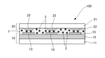
- FIG. 1 is a schematic view showing an example of the joined body of the present invention.
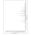
- FIG. 2 is a diagram showing a GC-MS analysis result of a polymerized compound of P-1M (phosphate acrylate) and KBE-903 (aminosilane coupling agent) in Examples.
- the anisotropic conductive film of the present invention comprises conductive particles, a film-forming resin, a radical polymerizable compound, a curing agent that generates free radicals, and an amine obtained from phosphoric acid (meth) acrylate and an amine-based silane coupling agent. It contains salt and further contains other components as required.
- the amine salt obtained from the phosphoric acid (meth) acrylate and the amine-based silane coupling agent is a mixture of phosphoric acid (meth) acrylate and amine-based silane coupling agent and polymerized by an acid-base reaction.
- it is an amine salt (polymerization compound) represented by the following formula. In the above formula, n represents 1 to 2, and a represents 1 to 2.
- phosphoric acid (meth) acrylate The phosphoric acid (meth) acrylate is not particularly limited and may be appropriately selected according to the purpose. For example, mono (2-methacryloyloxyethyl) acid phosphate, di (2-methacryloyloxyethyl) acid phosphate , Etc. Each of these acidities has a pH of less than 1.
- Specific examples of the phosphoric acid (meth) acrylate include compounds represented by the following general formula. However, in the above formula, R represents either a hydrogen atom, CH 2 Cl, and CH 3. n represents 1 to 6, and a represents 1 to 2. In the above formula, n represents 4 to 5, and a represents 1 to 2. In the above formula, n represents 1 to 2, a represents 1 to 2, and b represents 0 to 2.
- amine-based silane coupling agent examples include an aminosilane coupling agent and a ureidosilane coupling agent.
- aminosilane coupling agent include N-2- (aminoethyl) -3-aminopropylmethyldimethoxysilane, N-2- (aminoethyl) -3-aminopropyltrimethoxysilane, and N-2- (aminoethyl).
- ureidosilane coupling agent examples include 3-ureidopropyltriethoxysilane.
- the amine-based silane coupling agent has an acidity that is higher than 10 in pH.
- the reaction temperature is preferably controlled at 20 to 60 ° C., more preferably 40 to 50 ° C. When the reaction temperature is less than 20 ° C., the viscosity is high and the dispersion is subject to dispersibility, so that a local reaction is likely to occur and aggregates may be generated. On the other hand, when the reaction temperature exceeds 60 ° C., the reactivity becomes high, and similarly, aggregates are easily generated.
- the reaction is preferably performed in a state diluted with a solvent such as toluene.
- the mass ratio (A: B) of the phosphoric acid (meth) acrylate (A) and the amine-based silane coupling agent (B) is 7: 3 to 3:16, depending on the molecular weight of each. Is more preferable, and 5: 5 to 3:16 is more preferable. If the proportion of phosphoric acid (meth) acrylate is too large, good adhesion to the insulating film may not be obtained. If the proportion of the amine-based silane coupling agent is too large, the wiring material may be used. Good adhesive strength may not be obtained.
- the acidity of the amine salt is preferably pH 3 to 8, and more preferably 4 to 8.
- the pH can be measured using, for example, a pH meter.
- a polymerization inhibitor may be added to the amine salt to improve storage stability.
- the storage is preferably refrigerated storage.
- the content is preferably 0.1% by mass to 10% by mass, and more preferably 1% by mass to 5% by mass.
- the content is less than 0.1% by mass, the adhesion to both the highly polar wiring material and the highly hydrophobic insulating film may be lowered.
- the content exceeds 10% by mass, the highly polar wiring Adhesiveness to both the material and the highly hydrophobic insulating film is ensured, but the compatibility with the resin composition may be reduced and undissolved may occur.
- ⁇ Conductive particles> there is no restriction
- the metal particles include nickel, cobalt, silver, copper, gold, and palladium. These may be used individually by 1 type and may use 2 or more types together. Among these, nickel, silver, and copper are particularly preferable. In order to prevent these surface oxidations, particles having gold or palladium on the surface may be used. Furthermore, you may use what gave the insulating film with the metal protrusion and organic substance on the surface.
- the metal-coated resin particles include particles in which the surface of the resin core is coated with any metal of nickel, copper, gold, and palladium.
- the coating method of the metal to the said resin core there is no restriction
- the material for the resin core is not particularly limited and may be appropriately selected depending on the intended purpose. Examples thereof include styrene-divinylbenzene copolymer, benzoguanamine resin, cross-linked polystyrene resin, acrylic resin, and styrene-silica composite resin. Can be mentioned.
- the content of the conductive particles in the anisotropic conductive film is not particularly limited and can be appropriately adjusted depending on the wiring pitch of the circuit member, the connection area, and the like.
- the film-forming resin is not particularly limited and can be appropriately selected depending on the purpose.
- phenoxy resin, epoxy resin, unsaturated polyester resin, saturated polyester resin, urethane resin, butadiene resin, polyimide resin, polyamide resin And polyolefin resins may be used alone or in combination of two or more.
- phenoxy resin is particularly preferable from the viewpoints of film formability, processability, and connection reliability.
- the said phenoxy resin is resin synthesize
- the radical polymerizable compound is not particularly limited and may be appropriately selected depending on the intended purpose. Examples thereof include acrylic compounds and liquid acrylates, and specific examples include methyl acrylate, ethyl acrylate, isopropyl acrylate, and isobutyl.
- the curing agent is not particularly limited as long as it can cure the binder resin, and can be appropriately selected according to the purpose.
- a curing agent that generates free radicals by heat or light is preferable.
- an organic peroxide as a curing agent that generates free radicals by heat or light.
- the 1 minute half-life temperature is 90 ° C. to 180 ° C., and 10 hours half.
- An organic peroxide having an initial temperature of 40 ° C. or higher is preferred.
- the half-life temperature for 1 minute is preferably 180 ° C. or less, and if the 10-hour half-life temperature is 40 ° C.
- the curing agent that generates free radicals by light is a material that absorbs at an ultraviolet wavelength, and examples thereof include alkylphenone, benzoin, benzophenone, dicarbonyl compounds, thioxanthone, acylphosphine oxide, and derivatives thereof. These may be used individually by 1 type and may use 2 or more types together.
- the anisotropic conductive film includes, for example, conductive particles, a film-forming resin, a radical polymerizable compound, a curing agent that generates free radicals, and an amine salt obtained from phosphoric acid (meth) acrylate and an amine-based silane coupling agent. Further, it can be formed by preparing a coating solution containing other components (such as an organic solvent) if necessary, applying the coating solution on a substrate, and drying to remove the organic solvent.
- the thickness of the anisotropic conductive film is not particularly limited and may be appropriately selected depending on the purpose. For example, the thickness is preferably 1 ⁇ m to 50 ⁇ m, and more preferably 10 ⁇ m to 40 ⁇ m.
- the said anisotropic conductive film is arrange
- coating on a peeling film and drying There is no restriction
- a release PET (polyethylene terephthalate) sheet coated with a release agent such as silicone is preferable.
- a PTFE (polytetrafluoroethylene) sheet may be used.
- the joined body of the present invention includes the first circuit member, the second circuit member, and the anisotropic conductive film of the present invention, and further includes other members appropriately selected as necessary. Have. The first circuit member and the second circuit member are joined via the anisotropic conductive film.
- the first circuit member is not particularly limited as long as insulating films and wiring materials are alternately formed on the surface, and can be appropriately selected according to the purpose.
- the first circuit member has an insulating film on a substrate,
- a wiring material is formed on the insulating film at a predetermined interval, and the insulating film is exposed between the wiring materials.
- the present invention is not limited to the above, and it is sufficient if the insulating film and the wiring material are alternately formed on the surface of the first circuit member even if the wiring material is not formed on the insulating film.
- substrate There is no restriction
- Examples of the insulating film include SiNx and other organic insulating films.
- Examples of the wiring material of the first circuit member include metals such as aluminum, chromium, titanium, copper, and molybdenum; metal oxides (transparent electrode material) such as ITO and IZO, and the like. The above metals and metal oxides (transparent electrode material) may be laminated.
- the second circuit member has a wiring material or an electrode formed on a surface of the first circuit member facing the wiring material.
- Examples of the second circuit member include a flexible substrate having a wiring material and an IC chip.
- Examples of the wiring material or electrode of the second circuit member include NiSn plating or NiAu plating on Cu.
- connection method of the present invention includes a first circuit member in which insulating films and wiring materials are alternately formed on the surface; In the connection method with the second circuit member in which the wiring material or the electrode is formed on the surface facing the wiring material of the first circuit member, The anisotropic conductive film of the present invention is sandwiched between the first circuit member and the second circuit member, By pressing while heating from the first circuit member and the second circuit member, the anisotropic conductive film is cured, and the first circuit member and the second circuit member are connected. is there.
- Examples of the wiring material for the first circuit member include metals such as aluminum, chromium, titanium, copper, and molybdenum; metal oxides (transparent electrode material) such as ITO and IZO, and the like. These metals and metal oxides (transparent electrode material) may be laminated. Examples of the insulating film include SiNx and other organic insulating films. Examples of the wiring material or electrode of the second circuit member include NiSn plating or NiAu plating on Cu.
- the heating is determined by the total amount of heat, and when the joining is completed within a connection time of 10 seconds or less, the heating temperature is preferably 120 ° C to 220 ° C.
- the pressure bonding differs depending on the type of circuit member, and cannot be defined unconditionally. For example, in the case of TAB tape, the pressure is 2 MPa to 6 MPa, in the case of IC chip, the pressure is 20 MPa to 120 MPa, and in the case of COF, the pressure is 2 MPa to 6 MPa. Each of these is preferably performed for 3 to 10 seconds.
- the mass ratio of P-1M to KBE-903 (P-1M: KBE-903) is 7: 3 (pH 3.3) or more, preferably 5: 5 (pH 4.3) or more.
Landscapes
- Chemical & Material Sciences (AREA)
- Organic Chemistry (AREA)
- Health & Medical Sciences (AREA)
- Chemical Kinetics & Catalysis (AREA)
- Medicinal Chemistry (AREA)
- Polymers & Plastics (AREA)
- Non-Insulated Conductors (AREA)
- Adhesives Or Adhesive Processes (AREA)
- Adhesive Tapes (AREA)
- Conductive Materials (AREA)
Priority Applications (1)
| Application Number | Priority Date | Filing Date | Title |
|---|---|---|---|
| KR1020127030305A KR101437256B1 (ko) | 2010-04-20 | 2011-04-13 | 이방성 도전 필름, 접합체 및 접속 방법 |
Applications Claiming Priority (2)
| Application Number | Priority Date | Filing Date | Title |
|---|---|---|---|
| JP2010-097358 | 2010-04-20 | ||
| JP2010097358A JP5558184B2 (ja) | 2010-04-20 | 2010-04-20 | 異方性導電フィルム、接合体及び接続方法 |
Publications (1)
| Publication Number | Publication Date |
|---|---|
| WO2011132578A1 true WO2011132578A1 (ja) | 2011-10-27 |
Family
ID=42767265
Family Applications (1)
| Application Number | Title | Priority Date | Filing Date |
|---|---|---|---|
| PCT/JP2011/059146 Ceased WO2011132578A1 (ja) | 2010-04-20 | 2011-04-13 | 異方性導電フィルム、接合体及び接続方法 |
Country Status (4)
| Country | Link |
|---|---|
| JP (1) | JP5558184B2 (https=) |
| KR (1) | KR101437256B1 (https=) |
| TW (1) | TWI498410B (https=) |
| WO (1) | WO2011132578A1 (https=) |
Cited By (2)
| Publication number | Priority date | Publication date | Assignee | Title |
|---|---|---|---|---|
| WO2019245863A1 (en) * | 2018-06-18 | 2019-12-26 | Chemetall U.S., Inc. | Amine-functionalized organosilane / organophosphate combination systems as ep agents / corrosion inhibitors in compositions for treating metal surfaces |
| TWI781710B (zh) * | 2014-10-28 | 2022-10-21 | 日商迪睿合股份有限公司 | 異向性導電膜、其製造方法及連接構造體 |
Families Citing this family (1)
| Publication number | Priority date | Publication date | Assignee | Title |
|---|---|---|---|---|
| JP6782532B2 (ja) * | 2014-07-23 | 2020-11-11 | 日本乳化剤株式会社 | イオン結合性塩、イオン結合性塩組成物およびこれを含む樹脂組成物 |
Citations (2)
| Publication number | Priority date | Publication date | Assignee | Title |
|---|---|---|---|---|
| JP2003140179A (ja) * | 2001-10-31 | 2003-05-14 | Optrex Corp | 液晶表示パネルへの回路部品接続装置 |
| JP2004047228A (ja) * | 2002-07-10 | 2004-02-12 | Bridgestone Corp | 異方性導電フィルム及び電極付き基板の接着方法 |
Family Cites Families (3)
| Publication number | Priority date | Publication date | Assignee | Title |
|---|---|---|---|---|
| JPH11279424A (ja) * | 1998-03-26 | 1999-10-12 | Asahi Glass Co Ltd | 硬化性組成物 |
| KR100642445B1 (ko) * | 2004-12-29 | 2006-11-02 | 제일모직주식회사 | 이방 도전성 접착제용 수지 조성물 |
| JP5226562B2 (ja) * | 2008-03-27 | 2013-07-03 | デクセリアルズ株式会社 | 異方性導電フィルム、並びに、接合体及びその製造方法 |
-
2010
- 2010-04-20 JP JP2010097358A patent/JP5558184B2/ja active Active
-
2011
- 2011-04-13 WO PCT/JP2011/059146 patent/WO2011132578A1/ja not_active Ceased
- 2011-04-13 KR KR1020127030305A patent/KR101437256B1/ko not_active Expired - Fee Related
- 2011-04-19 TW TW100113519A patent/TWI498410B/zh not_active IP Right Cessation
Patent Citations (2)
| Publication number | Priority date | Publication date | Assignee | Title |
|---|---|---|---|---|
| JP2003140179A (ja) * | 2001-10-31 | 2003-05-14 | Optrex Corp | 液晶表示パネルへの回路部品接続装置 |
| JP2004047228A (ja) * | 2002-07-10 | 2004-02-12 | Bridgestone Corp | 異方性導電フィルム及び電極付き基板の接着方法 |
Cited By (3)
| Publication number | Priority date | Publication date | Assignee | Title |
|---|---|---|---|---|
| TWI781710B (zh) * | 2014-10-28 | 2022-10-21 | 日商迪睿合股份有限公司 | 異向性導電膜、其製造方法及連接構造體 |
| WO2019245863A1 (en) * | 2018-06-18 | 2019-12-26 | Chemetall U.S., Inc. | Amine-functionalized organosilane / organophosphate combination systems as ep agents / corrosion inhibitors in compositions for treating metal surfaces |
| US11396637B2 (en) | 2018-06-18 | 2022-07-26 | Chemetall U.S., Inc. | Amine-functionalized organosilane/organophosphate combination systems as EP agents / corrosion inhibitors in compositions for treating metal surfaces |
Also Published As
| Publication number | Publication date |
|---|---|
| TWI498410B (zh) | 2015-09-01 |
| JP5558184B2 (ja) | 2014-07-23 |
| TW201144405A (en) | 2011-12-16 |
| KR20130029770A (ko) | 2013-03-25 |
| KR101437256B1 (ko) | 2014-09-02 |
| JP2010186752A (ja) | 2010-08-26 |
Similar Documents
| Publication | Publication Date | Title |
|---|---|---|
| KR101085722B1 (ko) | 접속 필름, 및 접합체 및 그 제조 방법 | |
| JP5823117B2 (ja) | 異方性導電フィルム、接合体、及び接合体の製造方法 | |
| JP5685473B2 (ja) | 異方性導電フィルム、接合体の製造方法、及び接合体 | |
| JP5030196B2 (ja) | 回路接続用接着剤 | |
| JP5644067B2 (ja) | 絶縁被覆導電粒子 | |
| WO2012018123A1 (ja) | 異方導電性接着フィルムおよび硬化剤 | |
| JP5268260B2 (ja) | 異方導電性接着剤及び電気装置 | |
| JPH10168413A (ja) | 異方導電性接着剤 | |
| WO2012169498A1 (ja) | 異方性導電材料 | |
| JP5558184B2 (ja) | 異方性導電フィルム、接合体及び接続方法 | |
| JP2002285103A (ja) | 異方導電性接着剤 | |
| JP4735229B2 (ja) | 異方導電性フィルム | |
| JPH11209713A (ja) | 異方導電性接着剤 | |
| JP2016072239A (ja) | 異方性導電フィルム、及び接続方法 | |
| JP3947532B2 (ja) | 異方導電性接着剤フィルム | |
| JP2001254058A (ja) | 異方導電性接着剤 | |
| JP2002241722A (ja) | 異方導電性接着剤 | |
| JP2014086252A (ja) | 導電粒子及び異方導電性接着剤 | |
| TWI814761B (zh) | 接著劑膜 | |
| JP4730215B2 (ja) | 異方導電性接着剤フィルム | |
| JP6307294B2 (ja) | 回路接続材料、及び電子部品の製造方法 | |
| TWI921517B (zh) | 固化劑、接著劑組成物、電路連接用接著劑膜、連接結構體及連接結構體之製造方法 | |
| JP5328205B2 (ja) | 導電性微粒子、異方性導電材料、及び、導電接続構造体 | |
| JP5457655B2 (ja) | 導電性微粒子、異方性導電材料、及び、導電接続構造体 | |
| JP2002180012A (ja) | 異方導電性接着剤 |
Legal Events
| Date | Code | Title | Description |
|---|---|---|---|
| 121 | Ep: the epo has been informed by wipo that ep was designated in this application |
Ref document number: 11771913 Country of ref document: EP Kind code of ref document: A1 |
|
| DPE1 | Request for preliminary examination filed after expiration of 19th month from priority date (pct application filed from 20040101) | ||
| NENP | Non-entry into the national phase |
Ref country code: DE |
|
| ENP | Entry into the national phase |
Ref document number: 20127030305 Country of ref document: KR Kind code of ref document: A |
|
| 122 | Ep: pct application non-entry in european phase |
Ref document number: 11771913 Country of ref document: EP Kind code of ref document: A1 |