WO2011132578A1 - 異方性導電フィルム、接合体及び接続方法 - Google Patents
異方性導電フィルム、接合体及び接続方法 Download PDFInfo
- Publication number
- WO2011132578A1 WO2011132578A1 PCT/JP2011/059146 JP2011059146W WO2011132578A1 WO 2011132578 A1 WO2011132578 A1 WO 2011132578A1 JP 2011059146 W JP2011059146 W JP 2011059146W WO 2011132578 A1 WO2011132578 A1 WO 2011132578A1
- Authority
- WO
- WIPO (PCT)
- Prior art keywords
- circuit member
- conductive film
- anisotropic conductive
- amine
- coupling agent
- Prior art date
Links
Images
Classifications
-
- H—ELECTRICITY
- H01—ELECTRIC ELEMENTS
- H01L—SEMICONDUCTOR DEVICES NOT COVERED BY CLASS H10
- H01L24/00—Arrangements for connecting or disconnecting semiconductor or solid-state bodies; Methods or apparatus related thereto
- H01L24/01—Means for bonding being attached to, or being formed on, the surface to be connected, e.g. chip-to-package, die-attach, "first-level" interconnects; Manufacturing methods related thereto
- H01L24/26—Layer connectors, e.g. plate connectors, solder or adhesive layers; Manufacturing methods related thereto
- H01L24/28—Structure, shape, material or disposition of the layer connectors prior to the connecting process
- H01L24/29—Structure, shape, material or disposition of the layer connectors prior to the connecting process of an individual layer connector
-
- C—CHEMISTRY; METALLURGY
- C08—ORGANIC MACROMOLECULAR COMPOUNDS; THEIR PREPARATION OR CHEMICAL WORKING-UP; COMPOSITIONS BASED THEREON
- C08K—Use of inorganic or non-macromolecular organic substances as compounding ingredients
- C08K9/00—Use of pretreated ingredients
- C08K9/04—Ingredients treated with organic substances
-
- C—CHEMISTRY; METALLURGY
- C09—DYES; PAINTS; POLISHES; NATURAL RESINS; ADHESIVES; COMPOSITIONS NOT OTHERWISE PROVIDED FOR; APPLICATIONS OF MATERIALS NOT OTHERWISE PROVIDED FOR
- C09J—ADHESIVES; NON-MECHANICAL ASPECTS OF ADHESIVE PROCESSES IN GENERAL; ADHESIVE PROCESSES NOT PROVIDED FOR ELSEWHERE; USE OF MATERIALS AS ADHESIVES
- C09J11/00—Features of adhesives not provided for in group C09J9/00, e.g. additives
-
- C—CHEMISTRY; METALLURGY
- C09—DYES; PAINTS; POLISHES; NATURAL RESINS; ADHESIVES; COMPOSITIONS NOT OTHERWISE PROVIDED FOR; APPLICATIONS OF MATERIALS NOT OTHERWISE PROVIDED FOR
- C09J—ADHESIVES; NON-MECHANICAL ASPECTS OF ADHESIVE PROCESSES IN GENERAL; ADHESIVE PROCESSES NOT PROVIDED FOR ELSEWHERE; USE OF MATERIALS AS ADHESIVES
- C09J9/00—Adhesives characterised by their physical nature or the effects produced, e.g. glue sticks
- C09J9/02—Electrically-conducting adhesives
-
- C—CHEMISTRY; METALLURGY
- C09—DYES; PAINTS; POLISHES; NATURAL RESINS; ADHESIVES; COMPOSITIONS NOT OTHERWISE PROVIDED FOR; APPLICATIONS OF MATERIALS NOT OTHERWISE PROVIDED FOR
- C09J—ADHESIVES; NON-MECHANICAL ASPECTS OF ADHESIVE PROCESSES IN GENERAL; ADHESIVE PROCESSES NOT PROVIDED FOR ELSEWHERE; USE OF MATERIALS AS ADHESIVES
- C09J2203/00—Applications of adhesives in processes or use of adhesives in the form of films or foils
- C09J2203/326—Applications of adhesives in processes or use of adhesives in the form of films or foils for bonding electronic components such as wafers, chips or semiconductors
-
- H—ELECTRICITY
- H01—ELECTRIC ELEMENTS
- H01L—SEMICONDUCTOR DEVICES NOT COVERED BY CLASS H10
- H01L2224/00—Indexing scheme for arrangements for connecting or disconnecting semiconductor or solid-state bodies and methods related thereto as covered by H01L24/00
- H01L2224/01—Means for bonding being attached to, or being formed on, the surface to be connected, e.g. chip-to-package, die-attach, "first-level" interconnects; Manufacturing methods related thereto
- H01L2224/26—Layer connectors, e.g. plate connectors, solder or adhesive layers; Manufacturing methods related thereto
- H01L2224/28—Structure, shape, material or disposition of the layer connectors prior to the connecting process
- H01L2224/29—Structure, shape, material or disposition of the layer connectors prior to the connecting process of an individual layer connector
- H01L2224/29001—Core members of the layer connector
- H01L2224/29099—Material
- H01L2224/29198—Material with a principal constituent of the material being a combination of two or more materials in the form of a matrix with a filler, i.e. being a hybrid material, e.g. segmented structures, foams
- H01L2224/29199—Material of the matrix
- H01L2224/2929—Material of the matrix with a principal constituent of the material being a polymer, e.g. polyester, phenolic based polymer, epoxy
-
- H—ELECTRICITY
- H01—ELECTRIC ELEMENTS
- H01L—SEMICONDUCTOR DEVICES NOT COVERED BY CLASS H10
- H01L2224/00—Indexing scheme for arrangements for connecting or disconnecting semiconductor or solid-state bodies and methods related thereto as covered by H01L24/00
- H01L2224/01—Means for bonding being attached to, or being formed on, the surface to be connected, e.g. chip-to-package, die-attach, "first-level" interconnects; Manufacturing methods related thereto
- H01L2224/26—Layer connectors, e.g. plate connectors, solder or adhesive layers; Manufacturing methods related thereto
- H01L2224/28—Structure, shape, material or disposition of the layer connectors prior to the connecting process
- H01L2224/29—Structure, shape, material or disposition of the layer connectors prior to the connecting process of an individual layer connector
- H01L2224/29001—Core members of the layer connector
- H01L2224/29099—Material
- H01L2224/29198—Material with a principal constituent of the material being a combination of two or more materials in the form of a matrix with a filler, i.e. being a hybrid material, e.g. segmented structures, foams
- H01L2224/29298—Fillers
- H01L2224/29299—Base material
- H01L2224/293—Base material with a principal constituent of the material being a metal or a metalloid, e.g. boron [B], silicon [Si], germanium [Ge], arsenic [As], antimony [Sb], tellurium [Te] and polonium [Po], and alloys thereof
-
- H—ELECTRICITY
- H01—ELECTRIC ELEMENTS
- H01L—SEMICONDUCTOR DEVICES NOT COVERED BY CLASS H10
- H01L2224/00—Indexing scheme for arrangements for connecting or disconnecting semiconductor or solid-state bodies and methods related thereto as covered by H01L24/00
- H01L2224/73—Means for bonding being of different types provided for in two or more of groups H01L2224/10, H01L2224/18, H01L2224/26, H01L2224/34, H01L2224/42, H01L2224/50, H01L2224/63, H01L2224/71
- H01L2224/732—Location after the connecting process
- H01L2224/73201—Location after the connecting process on the same surface
- H01L2224/73203—Bump and layer connectors
- H01L2224/73204—Bump and layer connectors the bump connector being embedded into the layer connector
-
- H—ELECTRICITY
- H01—ELECTRIC ELEMENTS
- H01L—SEMICONDUCTOR DEVICES NOT COVERED BY CLASS H10
- H01L2224/00—Indexing scheme for arrangements for connecting or disconnecting semiconductor or solid-state bodies and methods related thereto as covered by H01L24/00
- H01L2224/80—Methods for connecting semiconductor or other solid state bodies using means for bonding being attached to, or being formed on, the surface to be connected
- H01L2224/83—Methods for connecting semiconductor or other solid state bodies using means for bonding being attached to, or being formed on, the surface to be connected using a layer connector
- H01L2224/838—Bonding techniques
- H01L2224/8385—Bonding techniques using a polymer adhesive, e.g. an adhesive based on silicone, epoxy, polyimide, polyester
- H01L2224/83851—Bonding techniques using a polymer adhesive, e.g. an adhesive based on silicone, epoxy, polyimide, polyester being an anisotropic conductive adhesive
-
- H—ELECTRICITY
- H01—ELECTRIC ELEMENTS
- H01L—SEMICONDUCTOR DEVICES NOT COVERED BY CLASS H10
- H01L2924/00—Indexing scheme for arrangements or methods for connecting or disconnecting semiconductor or solid-state bodies as covered by H01L24/00
- H01L2924/0001—Technical content checked by a classifier
- H01L2924/00011—Not relevant to the scope of the group, the symbol of which is combined with the symbol of this group
-
- H—ELECTRICITY
- H01—ELECTRIC ELEMENTS
- H01L—SEMICONDUCTOR DEVICES NOT COVERED BY CLASS H10
- H01L2924/00—Indexing scheme for arrangements or methods for connecting or disconnecting semiconductor or solid-state bodies as covered by H01L24/00
- H01L2924/01—Chemical elements
- H01L2924/01012—Magnesium [Mg]
-
- H—ELECTRICITY
- H01—ELECTRIC ELEMENTS
- H01L—SEMICONDUCTOR DEVICES NOT COVERED BY CLASS H10
- H01L2924/00—Indexing scheme for arrangements or methods for connecting or disconnecting semiconductor or solid-state bodies as covered by H01L24/00
- H01L2924/10—Details of semiconductor or other solid state devices to be connected
- H01L2924/11—Device type
- H01L2924/14—Integrated circuits
-
- H—ELECTRICITY
- H01—ELECTRIC ELEMENTS
- H01L—SEMICONDUCTOR DEVICES NOT COVERED BY CLASS H10
- H01L2924/00—Indexing scheme for arrangements or methods for connecting or disconnecting semiconductor or solid-state bodies as covered by H01L24/00
- H01L2924/15—Details of package parts other than the semiconductor or other solid state devices to be connected
- H01L2924/151—Die mounting substrate
- H01L2924/156—Material
- H01L2924/15786—Material with a principal constituent of the material being a non metallic, non metalloid inorganic material
- H01L2924/15788—Glasses, e.g. amorphous oxides, nitrides or fluorides
Definitions
- the present invention uses an anisotropic conductive film capable of electrically and mechanically connecting circuit members such as an IC chip and a liquid crystal panel (LCD panel) in a liquid crystal display (LCD), and the anisotropic conductive film.
- the present invention relates to a joined body and a connection method.
- a tape-like connection material for example, anisotropic conductive film (ACF)
- ACF anisotropic conductive film
- This anisotropic conductive film can be used for various purposes including connecting a terminal of a flexible printed circuit (FPC) or an IC chip to an ITO (Indium Tin Oxide) electrode formed on a glass substrate of an LCD panel. These terminals are used for bonding and electrically connecting the terminals.
- FPC flexible printed circuit
- ITO Indium Tin Oxide
- Patent Document 1 proposes a curing agent composition containing an amine salt compound having a silicon-containing group in which a hydroxyl group or a hydrolyzable group is bonded to a silicon atom.
- this proposal does not disclose or suggest an amine salt obtained from phosphoric acid (meth) acrylate and an amine-based silane coupling agent, and further improves adhesion strength to ACF and connection reliability.
- Patent Document 2 discloses an amine salt composed of phosphoric acid (meth) acrylate and tertiary amines, which is intended to reduce water content, improve adhesion, and be used for ACF. Is not disclosed or suggested.
- the present invention shows an anisotropic conductive film having good adhesion to both a highly polar wiring material and a highly hydrophobic insulating film, and improved storage stability, and a bonding using the anisotropic conductive film
- the object is to provide a body and a connection method.
- phosphoric acid (meth) acrylate is added to improve adhesion (adhesion), but when used alone, it has high hydrophobic insulation. Adhesion to the film was suppressed, and it was easy to stick to other materials (especially conductive particles) immediately. As a result, there was a drawback that the resistance value increased. On the other hand, when the amine-based silane coupling agent is added alone, the adhesion to the insulating film is improved, but the adhesion to the wiring material is lowered.
- the present invention is based on the above findings by the present inventors, and means for solving the above problems are as follows. That is, ⁇ 1> A conductive particle, a film-forming resin, a radical polymerizable compound, a curing agent that generates free radicals, and an amine salt obtained from phosphoric acid (meth) acrylate and an amine-based silane coupling agent An anisotropic conductive film. ⁇ 2> The anisotropic conductive film according to ⁇ 1>, wherein the amine salt has a pH of 3 to 8.
- ⁇ 3> a first circuit member in which insulating films and wiring materials are alternately formed on the surface;
- a second circuit member having a wiring material or an electrode formed on a surface thereof facing the wiring material of the first circuit member;
- An anisotropic conductive film according to any one of ⁇ 1> to ⁇ 2>, The joined body is characterized in that the first circuit member and the second circuit member are joined via the anisotropic conductive film.
- ⁇ 4> a first circuit member in which insulating films and wiring materials are alternately formed on the surface;
- the anisotropic conductive film according to any one of ⁇ 1> to ⁇ 2> is sandwiched between the first circuit member and the second circuit member, By pressing while heating from the first circuit member and the second circuit member, the anisotropic conductive film is cured, and the first circuit member and the second circuit member are connected. This is a characteristic connection method.
- the present invention it is possible to solve the above-mentioned problems and achieve the above-mentioned object, exhibit good adhesion to both a highly polar wiring material and a highly hydrophobic insulating film, and have storage stability.
- An improved anisotropic conductive film, a joined body using the anisotropic conductive film, and a connection method can be provided.
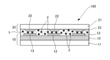
- FIG. 1 is a schematic view showing an example of the joined body of the present invention.
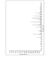
- FIG. 2 is a diagram showing a GC-MS analysis result of a polymerized compound of P-1M (phosphate acrylate) and KBE-903 (aminosilane coupling agent) in Examples.
- the anisotropic conductive film of the present invention comprises conductive particles, a film-forming resin, a radical polymerizable compound, a curing agent that generates free radicals, and an amine obtained from phosphoric acid (meth) acrylate and an amine-based silane coupling agent. It contains salt and further contains other components as required.
- the amine salt obtained from the phosphoric acid (meth) acrylate and the amine-based silane coupling agent is a mixture of phosphoric acid (meth) acrylate and amine-based silane coupling agent and polymerized by an acid-base reaction.
- it is an amine salt (polymerization compound) represented by the following formula. In the above formula, n represents 1 to 2, and a represents 1 to 2.
- phosphoric acid (meth) acrylate The phosphoric acid (meth) acrylate is not particularly limited and may be appropriately selected according to the purpose. For example, mono (2-methacryloyloxyethyl) acid phosphate, di (2-methacryloyloxyethyl) acid phosphate , Etc. Each of these acidities has a pH of less than 1.
- Specific examples of the phosphoric acid (meth) acrylate include compounds represented by the following general formula. However, in the above formula, R represents either a hydrogen atom, CH 2 Cl, and CH 3. n represents 1 to 6, and a represents 1 to 2. In the above formula, n represents 4 to 5, and a represents 1 to 2. In the above formula, n represents 1 to 2, a represents 1 to 2, and b represents 0 to 2.
- amine-based silane coupling agent examples include an aminosilane coupling agent and a ureidosilane coupling agent.
- aminosilane coupling agent include N-2- (aminoethyl) -3-aminopropylmethyldimethoxysilane, N-2- (aminoethyl) -3-aminopropyltrimethoxysilane, and N-2- (aminoethyl).
- ureidosilane coupling agent examples include 3-ureidopropyltriethoxysilane.
- the amine-based silane coupling agent has an acidity that is higher than 10 in pH.
- the reaction temperature is preferably controlled at 20 to 60 ° C., more preferably 40 to 50 ° C. When the reaction temperature is less than 20 ° C., the viscosity is high and the dispersion is subject to dispersibility, so that a local reaction is likely to occur and aggregates may be generated. On the other hand, when the reaction temperature exceeds 60 ° C., the reactivity becomes high, and similarly, aggregates are easily generated.
- the reaction is preferably performed in a state diluted with a solvent such as toluene.
- the mass ratio (A: B) of the phosphoric acid (meth) acrylate (A) and the amine-based silane coupling agent (B) is 7: 3 to 3:16, depending on the molecular weight of each. Is more preferable, and 5: 5 to 3:16 is more preferable. If the proportion of phosphoric acid (meth) acrylate is too large, good adhesion to the insulating film may not be obtained. If the proportion of the amine-based silane coupling agent is too large, the wiring material may be used. Good adhesive strength may not be obtained.
- the acidity of the amine salt is preferably pH 3 to 8, and more preferably 4 to 8.
- the pH can be measured using, for example, a pH meter.
- a polymerization inhibitor may be added to the amine salt to improve storage stability.
- the storage is preferably refrigerated storage.
- the content is preferably 0.1% by mass to 10% by mass, and more preferably 1% by mass to 5% by mass.
- the content is less than 0.1% by mass, the adhesion to both the highly polar wiring material and the highly hydrophobic insulating film may be lowered.
- the content exceeds 10% by mass, the highly polar wiring Adhesiveness to both the material and the highly hydrophobic insulating film is ensured, but the compatibility with the resin composition may be reduced and undissolved may occur.
- ⁇ Conductive particles> there is no restriction
- the metal particles include nickel, cobalt, silver, copper, gold, and palladium. These may be used individually by 1 type and may use 2 or more types together. Among these, nickel, silver, and copper are particularly preferable. In order to prevent these surface oxidations, particles having gold or palladium on the surface may be used. Furthermore, you may use what gave the insulating film with the metal protrusion and organic substance on the surface.
- the metal-coated resin particles include particles in which the surface of the resin core is coated with any metal of nickel, copper, gold, and palladium.
- the coating method of the metal to the said resin core there is no restriction
- the material for the resin core is not particularly limited and may be appropriately selected depending on the intended purpose. Examples thereof include styrene-divinylbenzene copolymer, benzoguanamine resin, cross-linked polystyrene resin, acrylic resin, and styrene-silica composite resin. Can be mentioned.
- the content of the conductive particles in the anisotropic conductive film is not particularly limited and can be appropriately adjusted depending on the wiring pitch of the circuit member, the connection area, and the like.
- the film-forming resin is not particularly limited and can be appropriately selected depending on the purpose.
- phenoxy resin, epoxy resin, unsaturated polyester resin, saturated polyester resin, urethane resin, butadiene resin, polyimide resin, polyamide resin And polyolefin resins may be used alone or in combination of two or more.
- phenoxy resin is particularly preferable from the viewpoints of film formability, processability, and connection reliability.
- the said phenoxy resin is resin synthesize
- the radical polymerizable compound is not particularly limited and may be appropriately selected depending on the intended purpose. Examples thereof include acrylic compounds and liquid acrylates, and specific examples include methyl acrylate, ethyl acrylate, isopropyl acrylate, and isobutyl.
- the curing agent is not particularly limited as long as it can cure the binder resin, and can be appropriately selected according to the purpose.
- a curing agent that generates free radicals by heat or light is preferable.
- an organic peroxide as a curing agent that generates free radicals by heat or light.
- the 1 minute half-life temperature is 90 ° C. to 180 ° C., and 10 hours half.
- An organic peroxide having an initial temperature of 40 ° C. or higher is preferred.
- the half-life temperature for 1 minute is preferably 180 ° C. or less, and if the 10-hour half-life temperature is 40 ° C.
- the curing agent that generates free radicals by light is a material that absorbs at an ultraviolet wavelength, and examples thereof include alkylphenone, benzoin, benzophenone, dicarbonyl compounds, thioxanthone, acylphosphine oxide, and derivatives thereof. These may be used individually by 1 type and may use 2 or more types together.
- the anisotropic conductive film includes, for example, conductive particles, a film-forming resin, a radical polymerizable compound, a curing agent that generates free radicals, and an amine salt obtained from phosphoric acid (meth) acrylate and an amine-based silane coupling agent. Further, it can be formed by preparing a coating solution containing other components (such as an organic solvent) if necessary, applying the coating solution on a substrate, and drying to remove the organic solvent.
- the thickness of the anisotropic conductive film is not particularly limited and may be appropriately selected depending on the purpose. For example, the thickness is preferably 1 ⁇ m to 50 ⁇ m, and more preferably 10 ⁇ m to 40 ⁇ m.
- the said anisotropic conductive film is arrange
- coating on a peeling film and drying There is no restriction
- a release PET (polyethylene terephthalate) sheet coated with a release agent such as silicone is preferable.
- a PTFE (polytetrafluoroethylene) sheet may be used.
- the joined body of the present invention includes the first circuit member, the second circuit member, and the anisotropic conductive film of the present invention, and further includes other members appropriately selected as necessary. Have. The first circuit member and the second circuit member are joined via the anisotropic conductive film.
- the first circuit member is not particularly limited as long as insulating films and wiring materials are alternately formed on the surface, and can be appropriately selected according to the purpose.
- the first circuit member has an insulating film on a substrate,
- a wiring material is formed on the insulating film at a predetermined interval, and the insulating film is exposed between the wiring materials.
- the present invention is not limited to the above, and it is sufficient if the insulating film and the wiring material are alternately formed on the surface of the first circuit member even if the wiring material is not formed on the insulating film.
- substrate There is no restriction
- Examples of the insulating film include SiNx and other organic insulating films.
- Examples of the wiring material of the first circuit member include metals such as aluminum, chromium, titanium, copper, and molybdenum; metal oxides (transparent electrode material) such as ITO and IZO, and the like. The above metals and metal oxides (transparent electrode material) may be laminated.
- the second circuit member has a wiring material or an electrode formed on a surface of the first circuit member facing the wiring material.
- Examples of the second circuit member include a flexible substrate having a wiring material and an IC chip.
- Examples of the wiring material or electrode of the second circuit member include NiSn plating or NiAu plating on Cu.
- connection method of the present invention includes a first circuit member in which insulating films and wiring materials are alternately formed on the surface; In the connection method with the second circuit member in which the wiring material or the electrode is formed on the surface facing the wiring material of the first circuit member, The anisotropic conductive film of the present invention is sandwiched between the first circuit member and the second circuit member, By pressing while heating from the first circuit member and the second circuit member, the anisotropic conductive film is cured, and the first circuit member and the second circuit member are connected. is there.
- Examples of the wiring material for the first circuit member include metals such as aluminum, chromium, titanium, copper, and molybdenum; metal oxides (transparent electrode material) such as ITO and IZO, and the like. These metals and metal oxides (transparent electrode material) may be laminated. Examples of the insulating film include SiNx and other organic insulating films. Examples of the wiring material or electrode of the second circuit member include NiSn plating or NiAu plating on Cu.
- the heating is determined by the total amount of heat, and when the joining is completed within a connection time of 10 seconds or less, the heating temperature is preferably 120 ° C to 220 ° C.
- the pressure bonding differs depending on the type of circuit member, and cannot be defined unconditionally. For example, in the case of TAB tape, the pressure is 2 MPa to 6 MPa, in the case of IC chip, the pressure is 20 MPa to 120 MPa, and in the case of COF, the pressure is 2 MPa to 6 MPa. Each of these is preferably performed for 3 to 10 seconds.
- the mass ratio of P-1M to KBE-903 (P-1M: KBE-903) is 7: 3 (pH 3.3) or more, preferably 5: 5 (pH 4.3) or more.
Abstract
導電性粒子、膜形成樹脂、ラジカル重合性化合物、遊離ラジカルを発生する硬化剤、及びリン酸(メタ)アクリレートとアミン系シランカップリング剤とから得られるアミン塩を含有する異方性導電フィルムを提供する。
Description
本発明は、ICチップ、液晶ディスプレイ(LCD)における液晶パネル(LCDパネル)等の回路部材を電気的かつ機械的に接続可能な異方性導電フィルム、並びに、該異方性導電フィルムを用いた接合体及び接続方法に関する。
従来より、回路部材を接続する手段として、導電性粒子が分散された熱硬化性樹脂を剥離フィルムに塗布したテープ状の接続材料(例えば、異方性導電フィルム(ACF;Anisotropic Conductive Film))が用いられている。
この異方性導電フィルムは、例えば、フレキシブルプリント基板(FPC)やICチップの端子と、LCDパネルのガラス基板上に形成されたITO(Indium Tin Oxide)電極とを接続する場合を始めとして、種々の端子同士を接着すると共に電気的に接続する場合に用いられている。
LCDパネルの接続部は、配線材及び絶縁膜が交互に配置され、構成されているが、従来のACFでは前記配線材及び前記絶縁膜に対する接着性が十分満足できるものではないという課題があった。
そこで、特許文献1には、ケイ素原子に水酸基又は加水分解性基が結合したケイ素含有基を有するアミン塩化合物を配合した硬化剤組成物が提案されている。
しかし、この提案には、リン酸(メタ)アクリレートとアミン系シランカップリング剤から得られるアミン塩については開示も示唆もなく、更に、ACFに対する接着強度、及び接続信頼性が向上することについても記載はない。
また、特許文献2には、リン酸(メタ)アクリレートと3級アミン類からなるアミン塩が開示されているが、含水低減を目的としたものであり、接着性向上すること、ACFに用いることについては開示も示唆もされていない。
そこで、特許文献1には、ケイ素原子に水酸基又は加水分解性基が結合したケイ素含有基を有するアミン塩化合物を配合した硬化剤組成物が提案されている。
しかし、この提案には、リン酸(メタ)アクリレートとアミン系シランカップリング剤から得られるアミン塩については開示も示唆もなく、更に、ACFに対する接着強度、及び接続信頼性が向上することについても記載はない。
また、特許文献2には、リン酸(メタ)アクリレートと3級アミン類からなるアミン塩が開示されているが、含水低減を目的としたものであり、接着性向上すること、ACFに用いることについては開示も示唆もされていない。
本発明は、従来における前記諸問題を解決し、以下の目的を達成することを課題とする。即ち、本発明は、極性の高い配線材及び疎水性の高い絶縁膜の双方に良好な接着性を示し、保存安定性が向上した異方性導電フィルム、該異方性導電フィルムを用いた接合体及び接続方法を提供することを目的とする。
前記課題を解決するため本発明者らが鋭意検討を重ねた結果、リン酸(メタ)アクリレートは密着力(接着力)を向上させるために添加されるが、単独で使用すると疎水性の高い絶縁膜への接着性が抑制され、すぐに他の材料(特に導電粒子)にくっつきやすく、その結果、抵抗値が上昇してしまうという欠点があった。一方、アミン系シランカップリング剤を単独で添加すると、絶縁膜への接着性は向上するが、配線材に対する接着性が低下してしまうという問題があった。
そこで、本発明者らが、更に鋭意検討を進めた結果、リン酸(メタ)アクリレートとアミン系シランカップリング剤とから得られるアミン塩を含有させることにより、極性の高い配線材と疎水性の高い絶縁膜への密着力を両立でき、アミン系シランカップリング剤の失活を防ぐことができるため保存安定性が向上し、導電性粒子表面へのリン酸(メタ)アクリレートの結合を防ぐことができるため低い導通抵抗(接続抵抗)が得られることを知見した。
そこで、本発明者らが、更に鋭意検討を進めた結果、リン酸(メタ)アクリレートとアミン系シランカップリング剤とから得られるアミン塩を含有させることにより、極性の高い配線材と疎水性の高い絶縁膜への密着力を両立でき、アミン系シランカップリング剤の失活を防ぐことができるため保存安定性が向上し、導電性粒子表面へのリン酸(メタ)アクリレートの結合を防ぐことができるため低い導通抵抗(接続抵抗)が得られることを知見した。
本発明は、本発明者らによる前記知見に基づくものであり、前記課題を解決するための手段としては、以下の通りである。即ち、
<1> 導電性粒子、膜形成樹脂、ラジカル重合性化合物、遊離ラジカルを発生する硬化剤、及びリン酸(メタ)アクリレートとアミン系シランカップリング剤とから得られるアミン塩を含有することを特徴とする異方性導電フィルムである。
<2> アミン塩のpHが3~8である前記<1>に記載の異方性導電フィルムである。
<3> 表面に絶縁膜と配線材が交互に形成された第1の回路部材と、
前記第1の回路部材の配線材と対向する面に配線材又は電極が形成された第2の回路部材と、
前記<1>から<2>のいずれかに記載の異方性導電フィルムと、を備え、
前記異方性導電フィルムを介して、前記第1の回路部材と前記第2の回路部材とが接合されていることを特徴とする接合体である。
<4> 表面に絶縁膜と配線材が交互に形成された第1の回路部材と、
前記第1の回路部材の配線材と対向する面に配線材又は電極が形成された第2の回路部材との接続方法において、
前記<1>から<2>のいずれかに記載の異方性導電フィルムが、前記第1の回路部材と第2の回路部材の間に挟持され、
前記第1の回路部材及び第2の回路部材から加熱しながら押圧することにより、前記異方性導電フィルムを硬化させて、前記第1の回路部材と前記第2の回路部材を接続することを特徴とする接続方法である。
本発明によれば、従来における前記諸問題を解決し、前記目的を達成することができ、極性の高い配線材及び疎水性の高い絶縁膜の双方に良好な接着性を示し、保存安定性が向上した異方性導電フィルム、該異方性導電フィルムを用いた接合体及び接続方法を提供することができる。
(異方性導電フィルム)
本発明の異方性導電フィルムは、導電性粒子、膜形成樹脂、ラジカル重合性化合物、遊離ラジカルを発生する硬化剤、及びリン酸(メタ)アクリレートとアミン系シランカップリング剤とから得られるアミン塩を含有してなり、更に必要に応じてその他の成分を含有してなる。
本発明の異方性導電フィルムは、導電性粒子、膜形成樹脂、ラジカル重合性化合物、遊離ラジカルを発生する硬化剤、及びリン酸(メタ)アクリレートとアミン系シランカップリング剤とから得られるアミン塩を含有してなり、更に必要に応じてその他の成分を含有してなる。
<リン酸(メタ)アクリレートとアミン系シランカップリング剤とから得られるアミン塩>
前記リン酸(メタ)アクリレートとアミン系シランカップリング剤とから得られるアミン塩は、リン酸(メタ)アクリレートとアミン系シランカップリング剤とを混合して、酸塩基反応で重合させたものであり、例えば下記式で表されるアミン塩(重合化合物)である。

ただし、前記式中、nは、1~2、aは、1~2を表す。
前記リン酸(メタ)アクリレートとアミン系シランカップリング剤とから得られるアミン塩は、リン酸(メタ)アクリレートとアミン系シランカップリング剤とを混合して、酸塩基反応で重合させたものであり、例えば下記式で表されるアミン塩(重合化合物)である。
-リン酸(メタ)アクリレート-
前記リン酸(メタ)アクリレートとしては、特に制限はなく、目的に応じて適否選択することができ、例えばモノ(2-メタクリロイルオキシエチル)アシッドフォスフェート、ジ(2-メタクリロイルオキシエチル)アシッドフォスフェート、などが挙げられる。
これらの酸性度は、いずれもpHが1より小さいものである。
前記リン酸(メタ)アクリレートの具体例としては、下記一般式で表される化合物などが挙げられる。

ただし、前記式中、Rは、水素原子、CH2Cl、及びCH3のいずれかを表す。nは、1~6、aは1~2を表す。

ただし、前記式中、nは、4~5、aは1~2を表す。

ただし、前記式中、nは、1~2、aは1~2、bは0~2を表す。
前記リン酸(メタ)アクリレートとしては、特に制限はなく、目的に応じて適否選択することができ、例えばモノ(2-メタクリロイルオキシエチル)アシッドフォスフェート、ジ(2-メタクリロイルオキシエチル)アシッドフォスフェート、などが挙げられる。
これらの酸性度は、いずれもpHが1より小さいものである。
前記リン酸(メタ)アクリレートの具体例としては、下記一般式で表される化合物などが挙げられる。
-アミン系シランカップリング剤-
前記アミン系シランカップリング剤としては、アミノシランカップリング剤と、ウレイドシランカップリング剤とがある。
前記アミノシランカップリング剤としては、例えばN-2-(アミノエチル)-3-アミノプロピルメチルジメトキシシラン、N-2-(アミノエチル)-3-アミノプロピルトリメトキシシラン、N-2-(アミノエチル)-3-アミノプロピルトリエトキシシラン、3-アミノプロピルトリメトキシシラン、3-アミノプロピルトリエトキシシラン、3-トリエトキシシリル-N-(1,3-ジメチル-ブチリデン)プロピルアミン、N-フェニル-3-アミノプロピルトリメトキシシラン、N-(ビニルベンジル)-2-アミノエチル-3-アミノプロピルトリメトキシシランなどが挙げられる。
前記ウレイドシランカップリング剤としては、例えば3-ウレイドプロピルトリエトキシシランなどが挙げられる。
前記アミン系シランカップリング剤は、酸性度が、いずれもpHが10よりも大きいものである。
-重合方法-
リン酸(メタ)アクリレートが強酸(pHが1未満)で、アミン系シランカップリング剤が強塩基(pHが10を超える)であるため、両者を混合するだけで酸塩基反応により容易に重合が進行する。触媒の添加は不要である。反応には発熱が伴うため少量滴下しながら重合を行うことが好ましい。反応温度は20℃~60℃で制御するのが好ましく、40℃~50℃がより好ましい。前記反応温度が20℃未満であると、粘度が高く、分散性にかけるため局所反応が起き易く凝集物が生成されることがある。一方、前記反応温度が60℃を超えると、反応性が高くなり、同様に凝集物が生成され易くなる。
前記反応は、トルエン等の溶剤に希釈した状態で行うことが好ましい。
前記リン酸(メタ)アクリレート(A)と前記アミン系シランカップリング剤(B)の質量比(A:B)は、それぞれの分子量などによっても異なるが、7:3~3:16であることが好ましく、5:5~3:16であることがより好ましい。前記リン酸(メタ)アクリレートの割合が多すぎると、絶縁膜に対して良好な接着力が得られなくなることがあり、前記アミン系シランカップリング剤の割合が多すぎると、配線材に対して良好な接着力が得られなくなることがある。
前記アミン塩の酸性度は、pH3~8であることが好ましく、4~8がより好ましい。前記pHが、3未満であると、絶縁膜に対して良好な接着力が得られなくなることがあり、8を超えると、配線材に対して良好な接着力が得られなくなることがある。
ここで、前記pHは、例えばpHメーターなどを用いて測定することができる。
前記アミン塩には、重合禁止剤を添加して保存安定性を高めてもよい。また、保管は冷蔵保存が好ましい。
前記リン酸(メタ)アクリレートと前記アミン系シランカップリング剤とから得られるアミン塩の前記異方性導電フィルムにおける含有量としては、特に制限はなく、目的に応じて適宜選択することができるが、例えば0.1質量%~10質量%であることが好ましく、1質量%~5質量%であることがより好ましい。前記含有量が、0.1質量%未満であると、極性の高い配線材、疎水性の高い絶縁膜双方への接着性が低下することがあり、10質量%を超えると、極性の高い配線材、疎水性の高い絶縁膜双方への接着性は確保されるが、樹脂組成物への相溶性が低下し、溶け残りが生じることがある。
<導電性粒子>
前記導電性粒子としては、特に制限はなく、目的に応じて適宜選択することができ、例えば金属粒子、金属被覆樹脂粒子などが挙げられる。
前記金属粒子としては、ニッケル、コバルト、銀、銅、金、パラジウムなどが挙げられる。これらは、1種単独で使用してもよいし、2種以上を併用してもよい。これらの中でも、ニッケル、銀、銅が特に好ましい。これらの表面酸化を防ぐ目的で、表面に金、パラジウムを施した粒子を用いてもよい。更に、表面に金属突起や有機物で絶縁皮膜を施したものを用いてもよい。
前記金属被覆樹脂粒子としては、樹脂コアの表面をニッケル、銅、金、及びパラジウムのいずれかの金属を被覆した粒子が挙げられる。同様に、最外表面に金、パラジウムを施した粒子を用いてもよい。更に、表面に金属突起や有機物で絶縁皮膜を施したものを用いてもよい。
前記樹脂コアへの金属の被覆方法としては、特に制限はなく、目的に応じて適宜選択することができ、例えば無電解めっき法、スパッタリング法、などが挙げられる。
前記樹脂コアの材料としては、特に制限はなく、目的に応じて適宜選択することができ、例えばスチレン-ジビニルベンゼン共重合体、ベンゾグアナミン樹脂、架橋ポリスチレン樹脂、アクリル樹脂、スチレン-シリカ複合樹脂などが挙げられる。
前記導電性粒子の前記異方性導電フィルムにおける含有量としては、特に制限はなく、回路部材の配線ピッチや、接続面積などによって適宜調整することができる。
<膜形成樹脂>
前記膜形成樹脂としては、特に制限はなく、目的に応じて適宜選択することができ、例えばフェノキシ樹脂、エポキシ樹脂、不飽和ポリエステル樹脂、飽和ポリエステル樹脂、ウレタン樹脂、ブタジエン樹脂、ポリイミド樹脂、ポリアミド樹脂、ポリオレフィン樹脂などが挙げられる。前記膜形成樹脂は、1種単独で使用してもよいし、2種以上を併用してもよい。これらの中でも、製膜性、加工性、接続信頼性の点からフェノキシ樹脂が特に好ましい。
前記フェノキシ樹脂とは、ビスフェノールAとエピクロルヒドリンより合成される樹脂であって、適宜合成したものを使用してもよいし、市販品を使用してもよい。
前記膜形成樹脂としては、特に制限はなく、目的に応じて適宜選択することができ、例えばフェノキシ樹脂、エポキシ樹脂、不飽和ポリエステル樹脂、飽和ポリエステル樹脂、ウレタン樹脂、ブタジエン樹脂、ポリイミド樹脂、ポリアミド樹脂、ポリオレフィン樹脂などが挙げられる。前記膜形成樹脂は、1種単独で使用してもよいし、2種以上を併用してもよい。これらの中でも、製膜性、加工性、接続信頼性の点からフェノキシ樹脂が特に好ましい。
前記フェノキシ樹脂とは、ビスフェノールAとエピクロルヒドリンより合成される樹脂であって、適宜合成したものを使用してもよいし、市販品を使用してもよい。
<ラジカル重合性化合物>
前記ラジカル重合性化合物としては、特に制限はなく、目的に応じて適宜選択することができ、例えばアクリル化合物、液状アクリレート等が例示され、具体的には、メチルアクリレート、エチルアクリレート、イソプロピルアクリレート、イソブチルアクリレート、エポキシアクリレート、エチレングリコールジアクリレート、ジエチレングリコールジアクリレート、トリメチロールプロパントリアクリレート、ジメチロールトリシクロデカンジアクリレート、テトラメチレングリコールテトラアクリレート、2-ヒドロキシ-1,3-ジアクリロキシプロパン、2,2-ビス[4-(アクリロキシメトキシ)フェニル]プロパン、2,2-ビス[4-(アクリロキシエトキシ)フェニル]プロパン、ジシクロペンテニルアクリレート、トリシクロデカニルアクリレート、トリス(アクリロキシエチル)イソシアヌレート、ウレタンアクリレート、エポキシアクリレートなどが挙げられる。なお、前記アクリレートをメタクリレートにしたものを用いることもできる。これらは、1種単独で使用してもよいし、2種以上を併用してもよい。
前記ラジカル重合性化合物としては、特に制限はなく、目的に応じて適宜選択することができ、例えばアクリル化合物、液状アクリレート等が例示され、具体的には、メチルアクリレート、エチルアクリレート、イソプロピルアクリレート、イソブチルアクリレート、エポキシアクリレート、エチレングリコールジアクリレート、ジエチレングリコールジアクリレート、トリメチロールプロパントリアクリレート、ジメチロールトリシクロデカンジアクリレート、テトラメチレングリコールテトラアクリレート、2-ヒドロキシ-1,3-ジアクリロキシプロパン、2,2-ビス[4-(アクリロキシメトキシ)フェニル]プロパン、2,2-ビス[4-(アクリロキシエトキシ)フェニル]プロパン、ジシクロペンテニルアクリレート、トリシクロデカニルアクリレート、トリス(アクリロキシエチル)イソシアヌレート、ウレタンアクリレート、エポキシアクリレートなどが挙げられる。なお、前記アクリレートをメタクリレートにしたものを用いることもできる。これらは、1種単独で使用してもよいし、2種以上を併用してもよい。
<硬化剤>
前記硬化剤としては、バインダー樹脂を硬化できるものであれば特に制限はなく、目的に応じて適宜選択することができるが、熱又は光によって遊離ラジカルを発生する硬化剤が好適である。
前記熱又は光によって遊離ラジカルを発生する硬化剤として有機過酸化物を用いることが好ましく、反応性と保存安定性の観点から1分間半減期温度が90℃~180℃であり、かつ10時間半減期温度が40℃以上である有機過酸化物が好適である。
10秒間以下で接続を行うためには1分間半減期温度が180℃以下であることが好ましく、10時間半減期温度が40℃以下であると冷蔵5℃以下の保管が困難となることがある。
光によって遊離ラジカルを発生する硬化剤としては、紫外線波長に吸収がある材料であり、例えばアルキルフェノン、ベンゾイン、ベンゾフェノン、ジカルボニル化合物、チオキサントン、アシルホスフィンオキサイド、又はこれらの誘導体などが挙げられる。これらは、1種単独で使用してもよいし、2種以上を併用してもよい。
-その他の成分-
前記その他の成分としては、特に制限はなく、目的に応じて適宜選択することができ、例えば充填剤、軟化剤、促進剤、老化防止剤、着色剤(顔料、染料)、有機溶剤、イオンキャッチャー剤などが挙げられる。前記その他の成分の添加量は、特に制限はなく、目的に応じて適宜選択することができる。
前記その他の成分としては、特に制限はなく、目的に応じて適宜選択することができ、例えば充填剤、軟化剤、促進剤、老化防止剤、着色剤(顔料、染料)、有機溶剤、イオンキャッチャー剤などが挙げられる。前記その他の成分の添加量は、特に制限はなく、目的に応じて適宜選択することができる。
前記異方性導電フィルムは、例えば導電性粒子、膜形成樹脂、ラジカル重合性化合物、遊離ラジカルを発生する硬化剤、及びリン酸(メタ)アクリレートとアミン系シランカップリング剤とから得られるアミン塩、更に必要に応じてその他の成分(有機溶媒等)を含有する塗布液を調製し、この塗布液を基材上に塗布し、乾燥させて有機溶媒を除去することにより形成することができる。
前記異方性導電フィルの厚みは、特に制限はなく、目的に応じて適宜選択することができ、例えば1μm~50μmであることが好ましく、10μm~40μmであることがより好ましい。
前記異方性導電フィルの厚みは、特に制限はなく、目的に応じて適宜選択することができ、例えば1μm~50μmであることが好ましく、10μm~40μmであることがより好ましい。
前記異方性導電フィルムは、剥離フィルム上に塗布し、乾燥することにより、剥離フィルム上に配置される。
前記剥離フィルムとしては、その形状、構造、大きさ、厚み、材料(材質)などについては、特に制限はなく、目的に応じて適宜選択することができるが、剥離性の良好なものや耐熱性が高いものが好ましく、例えば、シリコーン等の剥離剤が塗布された剥離PET(ポリエチレンテレフタレート)シートなどが好適に挙げられる。また、PTFE(ポリテトラフルオロエチレン)シートを用いてもよい。
前記剥離フィルムとしては、その形状、構造、大きさ、厚み、材料(材質)などについては、特に制限はなく、目的に応じて適宜選択することができるが、剥離性の良好なものや耐熱性が高いものが好ましく、例えば、シリコーン等の剥離剤が塗布された剥離PET(ポリエチレンテレフタレート)シートなどが好適に挙げられる。また、PTFE(ポリテトラフルオロエチレン)シートを用いてもよい。
(接合体)
本発明の接合体は、第1の回路部材と、第2の回路部材と、本発明の前記異方性導電フィルムとを有してなり、更に必要に応じて適宜選択した、その他の部材を有してなる。
前記異方性導電フィルムを介して、前記第1の回路部材と前記第2の回路部材とが接合されている。
本発明の接合体は、第1の回路部材と、第2の回路部材と、本発明の前記異方性導電フィルムとを有してなり、更に必要に応じて適宜選択した、その他の部材を有してなる。
前記異方性導電フィルムを介して、前記第1の回路部材と前記第2の回路部材とが接合されている。
<第1の回路部材>
前記第1の回路部材としては、表面に絶縁膜と配線材が交互に形成されていれば特に制限はなく、目的に応じて適宜選択することができ、例えば基板上に絶縁膜を有し、該絶縁膜上に配線材が所定間隔離間して形成され、配線材間には絶縁膜が露出している態様などが挙げられる。なお、上記に限定されず、絶縁膜上に配線材が形成されていなくても、第1の回路部材の表面において絶縁膜と配線材が交互に形成されていれば足りる。
前記基板としては、特に制限はなく、目的に応じて適宜選択することができるが、例えばガラス基板などが好ましい。
前記絶縁膜としては、例えばSiNx、その他有機系絶縁膜などが挙げられる。
前記第1の回路部材の配線材としては、例えば、アルミニウム、クロム、チタン、銅、モリブデン等の金属;ITO、IZO等の金属酸化物(透明電極材料)などが挙げられ、1種又は2種以上の金属、金属酸化物(透明電極材料)を積層させてもよい。
<第2の回路部材>
前記第2の回路部材は、前記第1の回路部材の配線材と対向する面に配線材又は電極が形成されたものであり、例えば配線材を有するフレキシブル基板、ICチップなどが挙げられる。
前記第2の回路部材の配線材又は電極としては、例えばCuにNiSnメッキ又はNiAuメッキなどが挙げられる。
前記第2の回路部材は、前記第1の回路部材の配線材と対向する面に配線材又は電極が形成されたものであり、例えば配線材を有するフレキシブル基板、ICチップなどが挙げられる。
前記第2の回路部材の配線材又は電極としては、例えばCuにNiSnメッキ又はNiAuメッキなどが挙げられる。
ここで、図1に示すように、第1の回路部材10は、ガラス基板11と、該基板上に絶縁層12と、該絶縁層上に配線材13が所定間隔離間して形成されている。
第2の回路部材20は、基板21と、該基板上に配線材又は電極22が所定間隔離間して形成されている。
接合体100は、第1の回路部材10と、第2の回路部材20と、本発明の前記異方性導電フィルム1とを有する。
第2の回路部材20の配線材又は電極22と、異方性導電フィルム1における導電性粒子2と、第1の回路部材10における配線材13とが導通することにより、第1の回路部材10と第2の回路部材20とが電気的に接続される。
第2の回路部材20は、基板21と、該基板上に配線材又は電極22が所定間隔離間して形成されている。
接合体100は、第1の回路部材10と、第2の回路部材20と、本発明の前記異方性導電フィルム1とを有する。
第2の回路部材20の配線材又は電極22と、異方性導電フィルム1における導電性粒子2と、第1の回路部材10における配線材13とが導通することにより、第1の回路部材10と第2の回路部材20とが電気的に接続される。
(接続方法)
本発明の接続方法は、表面に絶縁膜と配線材が交互に形成された第1の回路部材と、
前記第1の回路部材の配線材と対向する面に配線材又は電極が形成された第2の回路部材との接続方法において、
本発明の前記異方性導電フィルムが、前記第1の回路部材と第2の回路部材の間に挟持され、
前記第1の回路部材及び第2の回路部材から加熱しながら押圧することにより、前記異方性導電フィルムを硬化させて、前記第1の回路部材と前記第2の回路部材を接続するものである。
本発明の接続方法は、表面に絶縁膜と配線材が交互に形成された第1の回路部材と、
前記第1の回路部材の配線材と対向する面に配線材又は電極が形成された第2の回路部材との接続方法において、
本発明の前記異方性導電フィルムが、前記第1の回路部材と第2の回路部材の間に挟持され、
前記第1の回路部材及び第2の回路部材から加熱しながら押圧することにより、前記異方性導電フィルムを硬化させて、前記第1の回路部材と前記第2の回路部材を接続するものである。
前記第1の回路部材の配線材としては、例えばアルミニウム、クロム、チタン、銅、モリブデン等の金属;ITO、IZO等の金属酸化物(透明電極材料)などが挙げられ、1種又は2種以上の金属、金属酸化物(透明電極材料)を積層させてもよい。
前記絶縁膜としては、例えばSiNx、その他有機系絶縁膜などが挙げられる。
前記第2の回路部材の配線材又は電極としては、例えばCuにNiSnメッキ又はNiAuメッキなどが挙げられる。
前記絶縁膜としては、例えばSiNx、その他有機系絶縁膜などが挙げられる。
前記第2の回路部材の配線材又は電極としては、例えばCuにNiSnメッキ又はNiAuメッキなどが挙げられる。
-圧着条件-
前記加熱は、トータル熱量により決定され、接続時間10秒以下で接合を完了する場合には、加熱温度が120℃~220℃で行われることが好ましい。
前記圧着は、回路部材の種類によって異なり一概には規定できないが、例えばTABテープの場合には圧力2MPa~6MPa、ICチップの場合には圧力20MPa~120MPa、COFの場合には圧力2MPa~6MPaで、それぞれ3~10秒間行うことが好ましい。
前記加熱は、トータル熱量により決定され、接続時間10秒以下で接合を完了する場合には、加熱温度が120℃~220℃で行われることが好ましい。
前記圧着は、回路部材の種類によって異なり一概には規定できないが、例えばTABテープの場合には圧力2MPa~6MPa、ICチップの場合には圧力20MPa~120MPa、COFの場合には圧力2MPa~6MPaで、それぞれ3~10秒間行うことが好ましい。
以下、本発明の実施例について説明するが、本発明は下記実施例に何ら限定されるものではない。
(製造例1)
下記表1に示す組み合わせの配合量(質量部)により、リン酸アクリレートを氷浴中で冷却させながらアミン系シランカップリング剤を滴下し、攪拌した(合成には発熱を伴うため)。リン酸アクリレートとアミン系シランカップリング剤とから得られるアミン塩A1~A8を合成した。
得られた各アミン塩について、pHメーター(品名:HM-30P、東亞ディーケーケー株式会社製)を用いて酸性度の測定を行った。結果を表1に示す。
下記表1に示す組み合わせの配合量(質量部)により、リン酸アクリレートを氷浴中で冷却させながらアミン系シランカップリング剤を滴下し、攪拌した(合成には発熱を伴うため)。リン酸アクリレートとアミン系シランカップリング剤とから得られるアミン塩A1~A8を合成した。
得られた各アミン塩について、pHメーター(品名:HM-30P、東亞ディーケーケー株式会社製)を用いて酸性度の測定を行った。結果を表1に示す。

*リン酸アクリレート(P-2M):ジ-(2-メタクリロイルオキシエチル)アシッドフォスフェート、共栄社化学株式会社製、pH<1
*アミン系シランカップリング剤(KBE-903):N-2-(アミノエチル)3-アミノプロピルメチルジメトキシシラン、信越化学工業株式会社製、pH=10.5
*アミン系シランカップリング剤(KBM-573):N-フェニル-3-アミノプロピルトリメトキシシラン、信越化学工業株式会社製、pH=10.5
*アミン系シランカップリング剤(AY43-031):3-ウレイドプロピルトリエトキシシラン、東レ・ダウコーニング株式会社製、pH=10.1
<P-1M(リン酸アクリレート)とKBE-903(アミン系シランカップリング剤)から得られるアミン塩の分析結果>
-GC-MS分析-
・機器名:AGILENT TECHNOLOGIES社製 型番6890N/5975
・測定条件:試料10mgをTHF溶媒90mLに溶解しサンプルを作製した。試料溶液をGC-MSに1mL注入し測定を行った。気化条件280℃、カラム内温度40℃/5分間保持した後、昇温10℃/minで320℃まで昇温し、7分間保持して測定を終了した。
-GC-MS分析-
・機器名:AGILENT TECHNOLOGIES社製 型番6890N/5975
・測定条件:試料10mgをTHF溶媒90mLに溶解しサンプルを作製した。試料溶液をGC-MSに1mL注入し測定を行った。気化条件280℃、カラム内温度40℃/5分間保持した後、昇温10℃/minで320℃まで昇温し、7分間保持して測定を終了した。
以下の4種類について測定を行った。結果を図2に示す。
・リン酸アクリレート(P-1M)
・アミン系シランカップリング剤(KBE-903)
・アミン塩A2(P-1M:KBE-903=7:3(質量比))
・アミン塩A3(P-1M:KBE-903=5:5(質量比))
アミン塩A2には、KBE-903由来のピークは確認されなかったことから、P-1Mは全てアミン塩化されずに残存していることが分かった。
アミン塩A3には、KBE-903由来のピークが確認されたことから、P-1Mは全てアミン塩化され、アミン塩化の工程で消費されなかったKBE-903が全体面積の9.8%検出されたと考えられる。
よって、P-1MとKBE-903との質量比(P-1M:KBE-903)は、7:3(pH3.3)以上、好ましくは5:5(pH4.3)以上のKBE903を配合することでP-1Mをほぼ消失させることが可能となり、P-1Mの悪影響を受け難くできることが分かった。
-NMR分析-
・機器名 :VARIAN社製 品番マーキュリー300
・測定条件:試料5mgをCDCl3(重クロロホルム)0.75mLで溶解し、サンプルを作製した。積算回数は16回で待ち時間を5秒間で行った。
P-1Mと、KBE-903と、アミン塩(P-1M:KBE903=5:5(質量比))との3種類についてNMR分析を行った。
P-1MのA(-CH3)とB(=CH2)由来のピーク値を基準にしたときにアミン塩では-OH由来のピークが大幅に減少しているのが確認された。また、A(-CH3)とB(=CH2)の比率に変化がなかったことからB(=CH2)は反応していないことが分った。
同様にKBE-903の-CH2由来のピーク値を基準にしたときにアミン塩はNH2由来のピークにほとんど変化はみられないことが確認された。
よって、得られたアミン塩は、以下の構造式であることが推測される。なお、リン酸アクリレートには水酸基が2つあるので、2つの水酸基ともアミン塩化される場合もあるが、下記構造式では1つの水酸基のみアミン塩化された場合を示す。
(実施例1)
フェノキシ樹脂(品名:YP50、東都化成株式会社製)60質量部、ラジカル重合性樹脂(品名:EB-600、ダイセル・サイテック社製)35質量部、表1に記載のリン酸アクリレートとアミン系シランカップリング剤とから得られるアミン塩A1を3質量部、及び反応開始剤(品名:パーヘキサC、日本油脂株式会社製)2質量部で構成された接着剤中に、樹脂コアにNiAuメッキを施した平均粒子径4μmの導電性粒子(品名:AUL704、積水化学工業株式会社製)を粒子密度10,000個/mm2になるよう分散させて、厚み15μmの異方性導電膜S1を作製した。
フェノキシ樹脂(品名:YP50、東都化成株式会社製)60質量部、ラジカル重合性樹脂(品名:EB-600、ダイセル・サイテック社製)35質量部、表1に記載のリン酸アクリレートとアミン系シランカップリング剤とから得られるアミン塩A1を3質量部、及び反応開始剤(品名:パーヘキサC、日本油脂株式会社製)2質量部で構成された接着剤中に、樹脂コアにNiAuメッキを施した平均粒子径4μmの導電性粒子(品名:AUL704、積水化学工業株式会社製)を粒子密度10,000個/mm2になるよう分散させて、厚み15μmの異方性導電膜S1を作製した。
(実施例2)
実施例1において、リン酸アクリレートとアミン系シランカップリング剤とから得られるアミン塩A1を、表1に示すリン酸アクリレートとアミン系シランカップリング剤とから得られるアミン塩A2に代えた以外は、実施例1と同様にして、異方性導電膜S2を作製した。
実施例1において、リン酸アクリレートとアミン系シランカップリング剤とから得られるアミン塩A1を、表1に示すリン酸アクリレートとアミン系シランカップリング剤とから得られるアミン塩A2に代えた以外は、実施例1と同様にして、異方性導電膜S2を作製した。
(実施例3)
実施例1において、リン酸アクリレートとアミン系シランカップリング剤とから得られるアミン塩A1を、表1に示すリン酸アクリレートとアミン系シランカップリング剤とから得られるアミン塩A3に代えた以外は、実施例1と同様にして、異方性導電膜S3を作製した。
実施例1において、リン酸アクリレートとアミン系シランカップリング剤とから得られるアミン塩A1を、表1に示すリン酸アクリレートとアミン系シランカップリング剤とから得られるアミン塩A3に代えた以外は、実施例1と同様にして、異方性導電膜S3を作製した。
(実施例4)
実施例1において、リン酸アクリレートとアミン系シランカップリング剤とから得られるアミン塩A1を、表1に示すリン酸アクリレートとアミン系シランカップリング剤とから得られるアミン塩A4に代えた以外は、実施例1と同様にして、異方性導電膜S4を作製した。
実施例1において、リン酸アクリレートとアミン系シランカップリング剤とから得られるアミン塩A1を、表1に示すリン酸アクリレートとアミン系シランカップリング剤とから得られるアミン塩A4に代えた以外は、実施例1と同様にして、異方性導電膜S4を作製した。
(実施例5)
実施例1において、リン酸アクリレートとアミン系シランカップリング剤とから得られるアミン塩A1を、表1に示すリン酸アクリレートとアミン系シランカップリング剤とから得られるアミン塩A5に代えた以外は、実施例1と同様にして、異方性導電膜S5を作製した。
実施例1において、リン酸アクリレートとアミン系シランカップリング剤とから得られるアミン塩A1を、表1に示すリン酸アクリレートとアミン系シランカップリング剤とから得られるアミン塩A5に代えた以外は、実施例1と同様にして、異方性導電膜S5を作製した。
(実施例6)
実施例1において、リン酸アクリレートとアミン系シランカップリング剤とから得られるアミン塩A1を、表1に示すリン酸アクリレートとアミン系シランカップリング剤とから得られるアミン塩A6に代えた以外は、実施例1と同様にして、異方性導電膜S6を作製した。
実施例1において、リン酸アクリレートとアミン系シランカップリング剤とから得られるアミン塩A1を、表1に示すリン酸アクリレートとアミン系シランカップリング剤とから得られるアミン塩A6に代えた以外は、実施例1と同様にして、異方性導電膜S6を作製した。
(実施例7)
実施例1において、リン酸アクリレートとアミン系シランカップリング剤とから得られるアミン塩A1を、表1に示すリン酸アクリレートとアミン系シランカップリング剤とから得られるアミン塩A7に代えた以外は、実施例1と同様にして、異方性導電膜S7を作製した。
実施例1において、リン酸アクリレートとアミン系シランカップリング剤とから得られるアミン塩A1を、表1に示すリン酸アクリレートとアミン系シランカップリング剤とから得られるアミン塩A7に代えた以外は、実施例1と同様にして、異方性導電膜S7を作製した。
(実施例8)
実施例1において、リン酸アクリレートとアミン系シランカップリング剤とから得られるアミン塩A1を、表1に示すリン酸アクリレートとアミン系シランカップリング剤とから得られるアミン塩A8に代えた以外は、実施例1と同様にして、異方性導電膜S8を作製した。
実施例1において、リン酸アクリレートとアミン系シランカップリング剤とから得られるアミン塩A1を、表1に示すリン酸アクリレートとアミン系シランカップリング剤とから得られるアミン塩A8に代えた以外は、実施例1と同様にして、異方性導電膜S8を作製した。
(比較例1)
-リン酸アクリレート及びアミン系シランカップリング剤を含まない場合-
フェノキシ樹脂(品名:YP50、東都化成株式会社製)60質量部、ラジカル重合性樹脂(品名:EB-600、ダイセル・サイテック社製)35質量部、及び反応開始剤(品名:パーヘキサC、日本油脂株式会社製)2質量部で構成された接着剤中に導電性粒子(品名:AUL704、積水化学工業株式会社製)を粒子密度10,000個/mm2になるよう分散させて、厚み15μmの異方性導電膜R1を作製した。
-リン酸アクリレート及びアミン系シランカップリング剤を含まない場合-
フェノキシ樹脂(品名:YP50、東都化成株式会社製)60質量部、ラジカル重合性樹脂(品名:EB-600、ダイセル・サイテック社製)35質量部、及び反応開始剤(品名:パーヘキサC、日本油脂株式会社製)2質量部で構成された接着剤中に導電性粒子(品名:AUL704、積水化学工業株式会社製)を粒子密度10,000個/mm2になるよう分散させて、厚み15μmの異方性導電膜R1を作製した。
(比較例2)
-リン酸アクリレートのみを含む場合-
比較例1において、リン酸アクリレート(品名:P-1M、共栄社化学株式会社製)1質量部を配合した以外は、比較例1と同様にして、異方性導電膜R2を作製した。
-リン酸アクリレートのみを含む場合-
比較例1において、リン酸アクリレート(品名:P-1M、共栄社化学株式会社製)1質量部を配合した以外は、比較例1と同様にして、異方性導電膜R2を作製した。
(比較例3)
-アミン系シランカップリング剤のみを含む場合-
比較例1において、アミン系シランカップリング剤(品名:KBE-903、信越化学工業株式会社製)1質量部を配合した以外は、比較例1と同様にして、異方性導電膜R3を作製した。
-アミン系シランカップリング剤のみを含む場合-
比較例1において、アミン系シランカップリング剤(品名:KBE-903、信越化学工業株式会社製)1質量部を配合した以外は、比較例1と同様にして、異方性導電膜R3を作製した。
(比較例4)
-ウレイドシランカップリング剤のみを含む場合-
比較例1において、ウレイドシランカップリング剤(品名:AY43-031、東レダウコーニング株式会社製)1質量部を配合した以外は、比較例1と同様にして、異方性導電膜R4を作製した。
-ウレイドシランカップリング剤のみを含む場合-
比較例1において、ウレイドシランカップリング剤(品名:AY43-031、東レダウコーニング株式会社製)1質量部を配合した以外は、比較例1と同様にして、異方性導電膜R4を作製した。
(比較例5)
-リン酸アクリレート+イソシアネート系シランカップリング剤の場合(特開2003-282637号公報のイソシアネート系シランカップリング剤を使用)-
比較例1において、リン酸アクリレート(品名:P-1M、共栄社化学株式会社製)1質量部と、イソシアネート系シランカップリング剤(品名:Y5187、信越化学工業株式会社製)1質量部を単独で配合した以外は、比較例1と同様にして、異方性導電膜R5を作製した。
-リン酸アクリレート+イソシアネート系シランカップリング剤の場合(特開2003-282637号公報のイソシアネート系シランカップリング剤を使用)-
比較例1において、リン酸アクリレート(品名:P-1M、共栄社化学株式会社製)1質量部と、イソシアネート系シランカップリング剤(品名:Y5187、信越化学工業株式会社製)1質量部を単独で配合した以外は、比較例1と同様にして、異方性導電膜R5を作製した。
(比較例6)
-リン酸アクリレートとウレイドシランカップリング剤からアミン塩を事前に形成させずに、それぞれを系に配合した場合-
比較例1において、リン酸アクリレート(品名:P-1M、共栄社化学株式会社製)1質量部と、ウレイドシランカップリング剤(品名:AY43-031、東レダウコーニング株式会社製)1質量部を単独で配合した以外は、比較例1と同様にして、異方性導電膜R6を作製した。
-リン酸アクリレートとウレイドシランカップリング剤からアミン塩を事前に形成させずに、それぞれを系に配合した場合-
比較例1において、リン酸アクリレート(品名:P-1M、共栄社化学株式会社製)1質量部と、ウレイドシランカップリング剤(品名:AY43-031、東レダウコーニング株式会社製)1質量部を単独で配合した以外は、比較例1と同様にして、異方性導電膜R6を作製した。
(比較例7)
-リン酸アクリレートとアミン系シランカップリング剤からアミン塩を事前に形成させずに、それぞれを系に配合した場合-
比較例1において、リン酸アクリレート(品名:P-1M、共栄社化学株式会社製)1質量部と、アミン系シランカップリング剤(品名:KBE-903、信越化学工業株式会社製)1質量部を単独で配合した以外は、比較例1と同様にして、異方性導電膜R7を作製した。
-リン酸アクリレートとアミン系シランカップリング剤からアミン塩を事前に形成させずに、それぞれを系に配合した場合-
比較例1において、リン酸アクリレート(品名:P-1M、共栄社化学株式会社製)1質量部と、アミン系シランカップリング剤(品名:KBE-903、信越化学工業株式会社製)1質量部を単独で配合した以外は、比較例1と同様にして、異方性導電膜R7を作製した。
(比較例8)
-リン酸アクリレート+アミン系シランカップリング剤以外のアミン系化合物を用いた場合-
リン酸アクリレート(品名:P-1M、共栄社化学株式会社製)を攪拌しながらモノエタノールアミン塩(分子構造:NH3CH2OH)を滴下し、アミン塩B1を生成した。得られたアミン塩B1をpHメーター(品名:HM-30P、東亜ディーケーケー株式会社製)を用いて酸性度の測定を行ったところ、pHは7.2であった。
比較例1において、上記で作製したアミン塩B1 3質量部を用いた以外は、比較例1と同様にして、異方性導電膜R8を作製した。
-リン酸アクリレート+アミン系シランカップリング剤以外のアミン系化合物を用いた場合-
リン酸アクリレート(品名:P-1M、共栄社化学株式会社製)を攪拌しながらモノエタノールアミン塩(分子構造:NH3CH2OH)を滴下し、アミン塩B1を生成した。得られたアミン塩B1をpHメーター(品名:HM-30P、東亜ディーケーケー株式会社製)を用いて酸性度の測定を行ったところ、pHは7.2であった。
比較例1において、上記で作製したアミン塩B1 3質量部を用いた以外は、比較例1と同様にして、異方性導電膜R8を作製した。
<保存安定性の評価>
次に、作製直後(初期)の実施例1~8及び比較例1~8の各異方性導電膜と、30℃で60%RH環境下、48時間暴露後の各異方性導電膜とを用い、以下のようにして各実装体を作製し、以下のようにして、導通抵抗及び接着強度を測定した。そして、初期と、30℃で60%RH環境下、48時間暴露後との対比により、保存安定性を評価した。
次に、作製直後(初期)の実施例1~8及び比較例1~8の各異方性導電膜と、30℃で60%RH環境下、48時間暴露後の各異方性導電膜とを用い、以下のようにして各実装体を作製し、以下のようにして、導通抵抗及び接着強度を測定した。そして、初期と、30℃で60%RH環境下、48時間暴露後との対比により、保存安定性を評価した。
<実装体の作製>
評価基材として、COF(50μmP、Cu 8μmt-Snメッキ、38μmt-Sperflex基材)と、IZOコーティングガラス(全表面IZOコート、ガラス厚み0.7mm)の接合を行った。
実施例1~8及び比較例1~8の各異方性導電膜を1.5mm幅にスリットしてIZOコーティングガラスに貼り付けた。その上に、COFを仮固定した後、ヒートツール1.5mm幅で緩衝材として厚み100μmのテフロン(登録商標)を用いて、接合条件190℃、3MPaで10秒間接合を行い、各実装体を作製した。
また、IZOコーティングガラスをSiNxコーティングガラス(全表面SiNxコート、ガラス厚み0.7mm)に変更した以外は、同様にして、各実装体を作製した。
<実装体の導通抵抗の測定>
前記IZOコーティングガラスを用いて作製した各実装体について、初期(接続直後)と、85℃、85%RH、500時間後の導通抵抗を測定した。導通抵抗の測定は、デジタルマルチメータ(品番:デジタルマルチメータ7555、横河電機株式会社製)を用いて4端子法にて電流1mAを流したときの導通抵抗を測定した。各異方性導電膜を作製直後に接続を行った各実装体の結果を表2、及び各異方性導電膜を30℃で60%RH、48時間暴露した後に接続を行った各実装体の結果を表3に示す。
前記IZOコーティングガラスを用いて作製した各実装体について、初期(接続直後)と、85℃、85%RH、500時間後の導通抵抗を測定した。導通抵抗の測定は、デジタルマルチメータ(品番:デジタルマルチメータ7555、横河電機株式会社製)を用いて4端子法にて電流1mAを流したときの導通抵抗を測定した。各異方性導電膜を作製直後に接続を行った各実装体の結果を表2、及び各異方性導電膜を30℃で60%RH、48時間暴露した後に接続を行った各実装体の結果を表3に示す。
<実装体の接着強度の測定>
前記IZOコーティングガラス及び前記SiNxコーティングガラスを用いて作製した各実装体について、初期(接続直後)と、85℃、85%RHで500時間後の接着強度を測定した。接着強度は、引っ張り試験機(品番:RTC1201、AND社製)を用いて測定速度50mm/secでCOFを引き上げたときの接着強度を測定した。各異方性導電膜を作製直後に接続を行った各実装体の結果を表2、及び各異方性導電膜を30℃で60%RH、48時間暴露した後に接続を行った各実装体の結果を表3に示す。
前記IZOコーティングガラス及び前記SiNxコーティングガラスを用いて作製した各実装体について、初期(接続直後)と、85℃、85%RHで500時間後の接着強度を測定した。接着強度は、引っ張り試験機(品番:RTC1201、AND社製)を用いて測定速度50mm/secでCOFを引き上げたときの接着強度を測定した。各異方性導電膜を作製直後に接続を行った各実装体の結果を表2、及び各異方性導電膜を30℃で60%RH、48時間暴露した後に接続を行った各実装体の結果を表3に示す。
<<異方性導電膜を作製直後に接続を行った実装体の結果>>


<<異方性導電膜を30℃で60%RH、48時間暴露した後に接続を行った実装体の結果>>


表2及び表3の結果から、比較例1は、異方性導電膜を作製直後は特性を発現するが、保存安定性が悪いので、作製直後に比べて、異方性導電膜を30℃で60%RH、48時間暴露した後の接着強度が低下してしまうことが分かった。
また、リン酸アクリレートの配合量が多い場合には、導通抵抗が高くなり、IZOに対する接着力は向上するが、SiNxに対する接着力は低下する傾向があることが分かった。
また、アミン系シランカップリング剤の配合量が多い場合には、導通抵抗は低下し、SiNxに対する接着力は向上するが、IZOに対する接着力は低下するが傾向があることが分かった。
リン酸アクリレートとアミン系シランカップリング剤から生成したアミン塩を含有する異方性導電フィルムでは良好な導通信頼性、接着強度を示した(実施例1~8)。特にアミン塩のpHが3~8の範囲である、実施例2~4、及び実施例6~8では30℃で60%RH、48時間曝露試験後も良好な導通抵抗値、接着強度を示した。
一方、アミン塩を含有せず、アミン塩を生成する原料(リン酸アクリレート、アミン系シランカップリング剤)を含有しただけでは、良好な導通信頼性、接着性は得られなかった(比較例1~4)。また、アミン系シランカップリング剤以外のシランカップリング剤を使用した場合でも結果は同様であった(比較例4、5)。また、アミン塩の原料を配合したとしても、アミン塩を事前に形成させなかった場合も良好な結果は得られなかった(比較例6、7)。アミン塩であっても、リン酸アクリレートとアミン系シランカップリング剤以外から形成されたアミン塩では、良好な結果が得られなかった(比較例8)。
本発明の異方性導電フィルムは、例えばフレキシブルプリント基板(FPC)やICチップの端子とLCDパネルのガラス基板上に形成されたITO(Indium Tin Oxide)電極との接続、COFとPWBの接続、TCPとPWBの接続、COFとガラス基板の接続、COFとCOFの接続、IC基板とガラス基板の接続、IC基板とPWBの接続等の回路部材同士の接続に好適に用いられる。
1 異方性導電フィルム
2 導電性粒子
10 第1の回路部材
11 ガラス基板
12 絶縁膜
13 配線材
20 第2の回路部材
21 基板
22 配線材又は電極
100 接合体
2 導電性粒子
10 第1の回路部材
11 ガラス基板
12 絶縁膜
13 配線材
20 第2の回路部材
21 基板
22 配線材又は電極
100 接合体
Claims (4)
- 導電性粒子、膜形成樹脂、ラジカル重合性化合物、遊離ラジカルを発生する硬化剤、及びリン酸(メタ)アクリレートとアミン系シランカップリング剤とから得られるアミン塩を含有することを特徴とする異方性導電フィルム。
- アミン塩のpHが3~8である請求項1に記載の異方性導電フィルム。
- 表面に絶縁膜と配線材が交互に形成された第1の回路部材と、
前記第1の回路部材の配線材と対向する面に配線材又は電極が形成された第2の回路部材と、
請求項1から2のいずれかに記載の異方性導電フィルムと、を備え、
前記異方性導電フィルムを介して、前記第1の回路部材と前記第2の回路部材とが接合されていることを特徴とする接合体。 - 表面に絶縁膜と配線材が交互に形成された第1の回路部材と、
前記第1の回路部材の配線材と対向する面に配線材又は電極が形成された第2の回路部材との接続方法において、
請求項1から2のいずれかに記載の異方性導電フィルムが、前記第1の回路部材と第2の回路部材の間に挟持され、
前記第1の回路部材及び第2の回路部材から加熱しながら押圧することにより、前記異方性導電フィルムを硬化させて、前記第1の回路部材と前記第2の回路部材を接続することを特徴とする接続方法。
Priority Applications (1)
| Application Number | Priority Date | Filing Date | Title |
|---|---|---|---|
| KR1020127030305A KR101437256B1 (ko) | 2010-04-20 | 2011-04-13 | 이방성 도전 필름, 접합체 및 접속 방법 |
Applications Claiming Priority (2)
| Application Number | Priority Date | Filing Date | Title |
|---|---|---|---|
| JP2010-097358 | 2010-04-20 | ||
| JP2010097358A JP5558184B2 (ja) | 2010-04-20 | 2010-04-20 | 異方性導電フィルム、接合体及び接続方法 |
Publications (1)
| Publication Number | Publication Date |
|---|---|
| WO2011132578A1 true WO2011132578A1 (ja) | 2011-10-27 |
Family
ID=42767265
Family Applications (1)
| Application Number | Title | Priority Date | Filing Date |
|---|---|---|---|
| PCT/JP2011/059146 WO2011132578A1 (ja) | 2010-04-20 | 2011-04-13 | 異方性導電フィルム、接合体及び接続方法 |
Country Status (4)
| Country | Link |
|---|---|
| JP (1) | JP5558184B2 (ja) |
| KR (1) | KR101437256B1 (ja) |
| TW (1) | TWI498410B (ja) |
| WO (1) | WO2011132578A1 (ja) |
Cited By (2)
| Publication number | Priority date | Publication date | Assignee | Title |
|---|---|---|---|---|
| WO2019245863A1 (en) * | 2018-06-18 | 2019-12-26 | Chemetall U.S., Inc. | Amine-functionalized organosilane / organophosphate combination systems as ep agents / corrosion inhibitors in compositions for treating metal surfaces |
| TWI781710B (zh) * | 2014-10-28 | 2022-10-21 | 日商迪睿合股份有限公司 | 異向性導電膜、其製造方法及連接構造體 |
Families Citing this family (1)
| Publication number | Priority date | Publication date | Assignee | Title |
|---|---|---|---|---|
| JP6782532B2 (ja) * | 2014-07-23 | 2020-11-11 | 日本乳化剤株式会社 | イオン結合性塩、イオン結合性塩組成物およびこれを含む樹脂組成物 |
Citations (2)
| Publication number | Priority date | Publication date | Assignee | Title |
|---|---|---|---|---|
| JP2003140179A (ja) * | 2001-10-31 | 2003-05-14 | Optrex Corp | 液晶表示パネルへの回路部品接続装置 |
| JP2004047228A (ja) * | 2002-07-10 | 2004-02-12 | Bridgestone Corp | 異方性導電フィルム及び電極付き基板の接着方法 |
Family Cites Families (3)
| Publication number | Priority date | Publication date | Assignee | Title |
|---|---|---|---|---|
| JPH11279424A (ja) * | 1998-03-26 | 1999-10-12 | Asahi Glass Co Ltd | 硬化性組成物 |
| KR100642445B1 (ko) * | 2004-12-29 | 2006-11-02 | 제일모직주식회사 | 이방 도전성 접착제용 수지 조성물 |
| JP5226562B2 (ja) * | 2008-03-27 | 2013-07-03 | デクセリアルズ株式会社 | 異方性導電フィルム、並びに、接合体及びその製造方法 |
-
2010
- 2010-04-20 JP JP2010097358A patent/JP5558184B2/ja active Active
-
2011
- 2011-04-13 WO PCT/JP2011/059146 patent/WO2011132578A1/ja active Application Filing
- 2011-04-13 KR KR1020127030305A patent/KR101437256B1/ko not_active IP Right Cessation
- 2011-04-19 TW TW100113519A patent/TWI498410B/zh not_active IP Right Cessation
Patent Citations (2)
| Publication number | Priority date | Publication date | Assignee | Title |
|---|---|---|---|---|
| JP2003140179A (ja) * | 2001-10-31 | 2003-05-14 | Optrex Corp | 液晶表示パネルへの回路部品接続装置 |
| JP2004047228A (ja) * | 2002-07-10 | 2004-02-12 | Bridgestone Corp | 異方性導電フィルム及び電極付き基板の接着方法 |
Cited By (3)
| Publication number | Priority date | Publication date | Assignee | Title |
|---|---|---|---|---|
| TWI781710B (zh) * | 2014-10-28 | 2022-10-21 | 日商迪睿合股份有限公司 | 異向性導電膜、其製造方法及連接構造體 |
| WO2019245863A1 (en) * | 2018-06-18 | 2019-12-26 | Chemetall U.S., Inc. | Amine-functionalized organosilane / organophosphate combination systems as ep agents / corrosion inhibitors in compositions for treating metal surfaces |
| US11396637B2 (en) | 2018-06-18 | 2022-07-26 | Chemetall U.S., Inc. | Amine-functionalized organosilane/organophosphate combination systems as EP agents / corrosion inhibitors in compositions for treating metal surfaces |
Also Published As
| Publication number | Publication date |
|---|---|
| JP2010186752A (ja) | 2010-08-26 |
| JP5558184B2 (ja) | 2014-07-23 |
| TW201144405A (en) | 2011-12-16 |
| TWI498410B (zh) | 2015-09-01 |
| KR101437256B1 (ko) | 2014-09-02 |
| KR20130029770A (ko) | 2013-03-25 |
Similar Documents
| Publication | Publication Date | Title |
|---|---|---|
| KR101085722B1 (ko) | 접속 필름, 및 접합체 및 그 제조 방법 | |
| JP5030196B2 (ja) | 回路接続用接着剤 | |
| JP5823117B2 (ja) | 異方性導電フィルム、接合体、及び接合体の製造方法 | |
| JP5644067B2 (ja) | 絶縁被覆導電粒子 | |
| WO2013094543A1 (ja) | 導電性接着剤 | |
| WO2012018123A1 (ja) | 異方導電性接着フィルムおよび硬化剤 | |
| JP2007165052A (ja) | 異方導電性フィルム | |
| JP5268260B2 (ja) | 異方導電性接着剤及び電気装置 | |
| JP2011181525A (ja) | 異方性導電材料 | |
| JPH10168413A (ja) | 異方導電性接着剤 | |
| JP5558184B2 (ja) | 異方性導電フィルム、接合体及び接続方法 | |
| JP2018092943A (ja) | 導電材料及び接続構造体 | |
| JP2002285103A (ja) | 異方導電性接着剤 | |
| JP2010129960A (ja) | 接続フィルム、並びに、接合体及びその製造方法 | |
| JP3947532B2 (ja) | 異方導電性接着剤フィルム | |
| JPH11209713A (ja) | 異方導電性接着剤 | |
| JP2001254058A (ja) | 異方導電性接着剤 | |
| JP2002241722A (ja) | 異方導電性接着剤 | |
| JP2000044905A (ja) | 異方導電性接着剤及びそれを用いた電子機器 | |
| JP4730215B2 (ja) | 異方導電性接着剤フィルム | |
| TWI814761B (zh) | 接著劑膜 | |
| JP2016072239A (ja) | 異方性導電フィルム、及び接続方法 | |
| JP2014086252A (ja) | 導電粒子及び異方導電性接着剤 | |
| JP5328205B2 (ja) | 導電性微粒子、異方性導電材料、及び、導電接続構造体 | |
| WO2016163226A1 (ja) | 異方性導電フィルム、及び接続方法 |
Legal Events
| Date | Code | Title | Description |
|---|---|---|---|
| 121 | Ep: the epo has been informed by wipo that ep was designated in this application |
Ref document number: 11771913 Country of ref document: EP Kind code of ref document: A1 |
|
| DPE1 | Request for preliminary examination filed after expiration of 19th month from priority date (pct application filed from 20040101) | ||
| NENP | Non-entry into the national phase |
Ref country code: DE |
|
| ENP | Entry into the national phase |
Ref document number: 20127030305 Country of ref document: KR Kind code of ref document: A |
|
| 122 | Ep: pct application non-entry in european phase |
Ref document number: 11771913 Country of ref document: EP Kind code of ref document: A1 |