WO2011125928A1 - 半導体装置およびその製造方法 - Google Patents
半導体装置およびその製造方法 Download PDFInfo
- Publication number
- WO2011125928A1 WO2011125928A1 PCT/JP2011/058400 JP2011058400W WO2011125928A1 WO 2011125928 A1 WO2011125928 A1 WO 2011125928A1 JP 2011058400 W JP2011058400 W JP 2011058400W WO 2011125928 A1 WO2011125928 A1 WO 2011125928A1
- Authority
- WO
- WIPO (PCT)
- Prior art keywords
- film
- wiring
- nitride
- nitride film
- interlayer insulating
- Prior art date
- Legal status (The legal status is an assumption and is not a legal conclusion. Google has not performed a legal analysis and makes no representation as to the accuracy of the status listed.)
- Ceased
Links
Images








Classifications
-
- H—ELECTRICITY
- H10—SEMICONDUCTOR DEVICES; ELECTRIC SOLID-STATE DEVICES NOT OTHERWISE PROVIDED FOR
- H10W—GENERIC PACKAGES, INTERCONNECTIONS, CONNECTORS OR OTHER CONSTRUCTIONAL DETAILS OF DEVICES COVERED BY CLASS H10
- H10W20/00—Interconnections in chips, wafers or substrates
- H10W20/40—Interconnections external to wafers or substrates, e.g. back-end-of-line [BEOL] metallisations or vias connecting to gate electrodes
- H10W20/45—Interconnections external to wafers or substrates, e.g. back-end-of-line [BEOL] metallisations or vias connecting to gate electrodes characterised by their insulating parts
- H10W20/47—Interconnections external to wafers or substrates, e.g. back-end-of-line [BEOL] metallisations or vias connecting to gate electrodes characterised by their insulating parts comprising two or more dielectric layers having different properties, e.g. different dielectric constants
-
- H—ELECTRICITY
- H10—SEMICONDUCTOR DEVICES; ELECTRIC SOLID-STATE DEVICES NOT OTHERWISE PROVIDED FOR
- H10W—GENERIC PACKAGES, INTERCONNECTIONS, CONNECTORS OR OTHER CONSTRUCTIONAL DETAILS OF DEVICES COVERED BY CLASS H10
- H10W20/00—Interconnections in chips, wafers or substrates
- H10W20/01—Manufacture or treatment
- H10W20/031—Manufacture or treatment of conductive parts of the interconnections
- H10W20/063—Manufacture or treatment of conductive parts of the interconnections by forming conductive members before forming protective insulating material
-
- H—ELECTRICITY
- H10—SEMICONDUCTOR DEVICES; ELECTRIC SOLID-STATE DEVICES NOT OTHERWISE PROVIDED FOR
- H10W—GENERIC PACKAGES, INTERCONNECTIONS, CONNECTORS OR OTHER CONSTRUCTIONAL DETAILS OF DEVICES COVERED BY CLASS H10
- H10W20/00—Interconnections in chips, wafers or substrates
- H10W20/01—Manufacture or treatment
- H10W20/071—Manufacture or treatment of dielectric parts thereof
- H10W20/074—Manufacture or treatment of dielectric parts thereof of dielectric parts comprising thin functional dielectric layers, e.g. dielectric etch-stop, barrier, capping or liner layers
- H10W20/075—Manufacture or treatment of dielectric parts thereof of dielectric parts comprising thin functional dielectric layers, e.g. dielectric etch-stop, barrier, capping or liner layers of multilayered thin functional dielectric layers
-
- H—ELECTRICITY
- H10—SEMICONDUCTOR DEVICES; ELECTRIC SOLID-STATE DEVICES NOT OTHERWISE PROVIDED FOR
- H10W—GENERIC PACKAGES, INTERCONNECTIONS, CONNECTORS OR OTHER CONSTRUCTIONAL DETAILS OF DEVICES COVERED BY CLASS H10
- H10W20/00—Interconnections in chips, wafers or substrates
- H10W20/01—Manufacture or treatment
- H10W20/071—Manufacture or treatment of dielectric parts thereof
- H10W20/074—Manufacture or treatment of dielectric parts thereof of dielectric parts comprising thin functional dielectric layers, e.g. dielectric etch-stop, barrier, capping or liner layers
- H10W20/077—Manufacture or treatment of dielectric parts thereof of dielectric parts comprising thin functional dielectric layers, e.g. dielectric etch-stop, barrier, capping or liner layers on sidewalls or on top surfaces of conductors
-
- H—ELECTRICITY
- H10—SEMICONDUCTOR DEVICES; ELECTRIC SOLID-STATE DEVICES NOT OTHERWISE PROVIDED FOR
- H10W—GENERIC PACKAGES, INTERCONNECTIONS, CONNECTORS OR OTHER CONSTRUCTIONAL DETAILS OF DEVICES COVERED BY CLASS H10
- H10W20/00—Interconnections in chips, wafers or substrates
- H10W20/40—Interconnections external to wafers or substrates, e.g. back-end-of-line [BEOL] metallisations or vias connecting to gate electrodes
- H10W20/41—Interconnections external to wafers or substrates, e.g. back-end-of-line [BEOL] metallisations or vias connecting to gate electrodes characterised by their conductive parts
- H10W20/425—Barrier, adhesion or liner layers
-
- H—ELECTRICITY
- H10—SEMICONDUCTOR DEVICES; ELECTRIC SOLID-STATE DEVICES NOT OTHERWISE PROVIDED FOR
- H10W—GENERIC PACKAGES, INTERCONNECTIONS, CONNECTORS OR OTHER CONSTRUCTIONAL DETAILS OF DEVICES COVERED BY CLASS H10
- H10W20/00—Interconnections in chips, wafers or substrates
- H10W20/40—Interconnections external to wafers or substrates, e.g. back-end-of-line [BEOL] metallisations or vias connecting to gate electrodes
- H10W20/41—Interconnections external to wafers or substrates, e.g. back-end-of-line [BEOL] metallisations or vias connecting to gate electrodes characterised by their conductive parts
- H10W20/435—Cross-sectional shapes or dispositions of interconnections
-
- H—ELECTRICITY
- H10—SEMICONDUCTOR DEVICES; ELECTRIC SOLID-STATE DEVICES NOT OTHERWISE PROVIDED FOR
- H10W—GENERIC PACKAGES, INTERCONNECTIONS, CONNECTORS OR OTHER CONSTRUCTIONAL DETAILS OF DEVICES COVERED BY CLASS H10
- H10W74/00—Encapsulations, e.g. protective coatings
- H10W74/10—Encapsulations, e.g. protective coatings characterised by their shape or disposition
- H10W74/131—Encapsulations, e.g. protective coatings characterised by their shape or disposition the semiconductor body being only partially enclosed
- H10W74/137—Encapsulations, e.g. protective coatings characterised by their shape or disposition the semiconductor body being only partially enclosed the encapsulations being directly on the semiconductor body
-
- H—ELECTRICITY
- H10—SEMICONDUCTOR DEVICES; ELECTRIC SOLID-STATE DEVICES NOT OTHERWISE PROVIDED FOR
- H10W—GENERIC PACKAGES, INTERCONNECTIONS, CONNECTORS OR OTHER CONSTRUCTIONAL DETAILS OF DEVICES COVERED BY CLASS H10
- H10W74/00—Encapsulations, e.g. protective coatings
- H10W74/10—Encapsulations, e.g. protective coatings characterised by their shape or disposition
- H10W74/131—Encapsulations, e.g. protective coatings characterised by their shape or disposition the semiconductor body being only partially enclosed
- H10W74/147—Encapsulations, e.g. protective coatings characterised by their shape or disposition the semiconductor body being only partially enclosed the encapsulations being multilayered
-
- H—ELECTRICITY
- H10—SEMICONDUCTOR DEVICES; ELECTRIC SOLID-STATE DEVICES NOT OTHERWISE PROVIDED FOR
- H10W—GENERIC PACKAGES, INTERCONNECTIONS, CONNECTORS OR OTHER CONSTRUCTIONAL DETAILS OF DEVICES COVERED BY CLASS H10
- H10W70/00—Package substrates; Interposers; Redistribution layers [RDL]
- H10W70/60—Insulating or insulated package substrates; Interposers; Redistribution layers
-
- H—ELECTRICITY
- H10—SEMICONDUCTOR DEVICES; ELECTRIC SOLID-STATE DEVICES NOT OTHERWISE PROVIDED FOR
- H10W—GENERIC PACKAGES, INTERCONNECTIONS, CONNECTORS OR OTHER CONSTRUCTIONAL DETAILS OF DEVICES COVERED BY CLASS H10
- H10W72/00—Interconnections or connectors in packages
- H10W72/01—Manufacture or treatment
- H10W72/019—Manufacture or treatment of bond pads
- H10W72/01951—Changing the shapes of bond pads
- H10W72/01955—Changing the shapes of bond pads by using masks
-
- H—ELECTRICITY
- H10—SEMICONDUCTOR DEVICES; ELECTRIC SOLID-STATE DEVICES NOT OTHERWISE PROVIDED FOR
- H10W—GENERIC PACKAGES, INTERCONNECTIONS, CONNECTORS OR OTHER CONSTRUCTIONAL DETAILS OF DEVICES COVERED BY CLASS H10
- H10W72/00—Interconnections or connectors in packages
- H10W72/50—Bond wires
- H10W72/531—Shapes of wire connectors
- H10W72/536—Shapes of wire connectors the connected ends being ball-shaped
-
- H—ELECTRICITY
- H10—SEMICONDUCTOR DEVICES; ELECTRIC SOLID-STATE DEVICES NOT OTHERWISE PROVIDED FOR
- H10W—GENERIC PACKAGES, INTERCONNECTIONS, CONNECTORS OR OTHER CONSTRUCTIONAL DETAILS OF DEVICES COVERED BY CLASS H10
- H10W72/00—Interconnections or connectors in packages
- H10W72/50—Bond wires
- H10W72/551—Materials of bond wires
- H10W72/552—Materials of bond wires comprising metals or metalloids, e.g. silver
- H10W72/5522—Materials of bond wires comprising metals or metalloids, e.g. silver comprising gold [Au]
-
- H—ELECTRICITY
- H10—SEMICONDUCTOR DEVICES; ELECTRIC SOLID-STATE DEVICES NOT OTHERWISE PROVIDED FOR
- H10W—GENERIC PACKAGES, INTERCONNECTIONS, CONNECTORS OR OTHER CONSTRUCTIONAL DETAILS OF DEVICES COVERED BY CLASS H10
- H10W72/00—Interconnections or connectors in packages
- H10W72/50—Bond wires
- H10W72/59—Bond pads specially adapted therefor
-
- H—ELECTRICITY
- H10—SEMICONDUCTOR DEVICES; ELECTRIC SOLID-STATE DEVICES NOT OTHERWISE PROVIDED FOR
- H10W—GENERIC PACKAGES, INTERCONNECTIONS, CONNECTORS OR OTHER CONSTRUCTIONAL DETAILS OF DEVICES COVERED BY CLASS H10
- H10W72/00—Interconnections or connectors in packages
- H10W72/90—Bond pads, in general
- H10W72/921—Structures or relative sizes of bond pads
- H10W72/923—Bond pads having multiple stacked layers
-
- H—ELECTRICITY
- H10—SEMICONDUCTOR DEVICES; ELECTRIC SOLID-STATE DEVICES NOT OTHERWISE PROVIDED FOR
- H10W—GENERIC PACKAGES, INTERCONNECTIONS, CONNECTORS OR OTHER CONSTRUCTIONAL DETAILS OF DEVICES COVERED BY CLASS H10
- H10W72/00—Interconnections or connectors in packages
- H10W72/90—Bond pads, in general
- H10W72/931—Shapes of bond pads
- H10W72/934—Cross-sectional shape, i.e. in side view
-
- H—ELECTRICITY
- H10—SEMICONDUCTOR DEVICES; ELECTRIC SOLID-STATE DEVICES NOT OTHERWISE PROVIDED FOR
- H10W—GENERIC PACKAGES, INTERCONNECTIONS, CONNECTORS OR OTHER CONSTRUCTIONAL DETAILS OF DEVICES COVERED BY CLASS H10
- H10W72/00—Interconnections or connectors in packages
- H10W72/90—Bond pads, in general
- H10W72/951—Materials of bond pads
- H10W72/952—Materials of bond pads comprising metals or metalloids, e.g. PbSn, Ag or Cu
Definitions
- the present invention relates to a semiconductor device having wiring made of a material mainly composed of copper on an interlayer insulating film, and a method for manufacturing the same.
- Non-Patent Document 1 proposes a structure using copper wiring as the uppermost layer wiring.
- the uppermost layer wiring of the power device is composed of copper wiring
- an organic film formed by coating polyimide or other resin material is applied to the passivation film covering the copper wiring. This is to fill a large step between the thick copper wiring and its surroundings.
- the cost required for forming the organic film is high. Therefore, it is conceivable to use an inorganic film.
- a silicon oxide film which is a typical example of an inorganic film cannot be used as a film in contact with a copper wiring. This is because copper easily diffuses into silicon oxide.
- a silicon nitride film, which is another example of the inorganic film, can prevent diffusion of copper and can be used as a film in contact with the copper wiring.
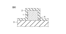
- the inventor of the present application conducted an experiment to form a silicon nitride film 2 so as to cover the thick film copper wiring 1 as shown in FIG.
- the fabricated structure was observed with a microscope, it was found that there was a problem that cracks were likely to occur in the silicon nitride film 2 in the vicinity of the lower corner portion 4 where the thick film copper wiring 1 and the uppermost interlayer insulating film 3 were in contact. This is considered to be caused by stress concentration in the silicon nitride film 2 in the vicinity of the lower corner portion 4. If the thickness of the silicon nitride film 2 is reduced, the problem of stress concentration is alleviated, but in order to prevent moisture from entering, it is necessary to secure a thickness of about 1 ⁇ m or more.
- An object of the present invention is to provide a semiconductor device that overcomes the above-described problems and a method for manufacturing the same.
- the semiconductor device of the present invention includes an interlayer insulating film, a wiring formed to protrude from the interlayer insulating film, and made of a material whose main component is copper, and a passivation film formed so as to cover the wiring.
- the passivation film is a laminated film in which a first nitride film, an intermediate film, and a second nitride film are laminated in order from the wiring side.
- the intermediate film is made of an insulating material different from that of the first and second nitride films.
- the passivation film is formed of a laminated film in which the intermediate film is sandwiched between the first and second nitride films. Since the first nitride film is disposed on the wiring (hereinafter referred to as “copper wiring”) having copper as a main component, copper diffusion can be prevented by the first nitride film.
- the intermediate film relaxes the stress of the first nitride film and further contributes to the thickening of the passivation film. Furthermore, since the second nitride film is laminated on the intermediate film, entry of moisture and other foreign matters can be effectively prevented.
- the copper wiring can be protected by the passivation film having a sufficient film thickness while relaxing the stress of the first nitride film by the intermediate film and suppressing the crack. Since the passivation film is made of an inorganic material, it can be formed at low cost.
- the passivation film made of a laminated film can have a sufficient thickness as a whole. Therefore, since the stress of the first nitride film can be further reduced by forming the first nitride film thin, it is possible to further suppress the occurrence of cracks in the first nitride film.
- the copper wiring may have a thickness of 10 ⁇ m or more (for example, 10 ⁇ m to 20 ⁇ m). By covering such a thick film copper wiring with the passivation film as described above, it is possible to suppress the occurrence of cracks in the passivation film in the vicinity of the contact portion between the thick film copper wiring and the interlayer insulating film. Can be sufficiently protected.
- the copper wiring may have a width of 10 ⁇ m or more (for example, 10 ⁇ m to 20 ⁇ m).
- a wide (preferably even thicker) copper wiring may be a power wiring of a power device.
- the copper wiring may be a top layer wiring.
- the “material mainly composed of copper” for forming the copper wiring for example, copper having a purity of 99.9% or more and a copper alloy to which Al, Ti, Ag, or the like is added can be used.
- the intermediate film is preferably a buffer film made of a material having a stress smaller than that of the material of the first nitride film. With this configuration, the stress generated in the first nitride film can be effectively relaxed.
- the intermediate film may be an oxide film (a silicon oxide film, a silicon oxynitride film, or the like).
- the diffusion of copper into the oxide film is blocked by the nitride film.
- the oxide film has a lower stress than the nitride film, the stress generated in the first nitride film can be relaxed and the occurrence of cracks in the first nitride film can be suppressed.
- the semiconductor device further includes a barrier film that is formed on the interlayer insulating film and prevents copper in the wiring from diffusing into the interlayer insulating film.
- the wiring has an overhang formed on the barrier film and protruding from the edge of the barrier film.
- Such an overhang portion inevitably occurs, for example, when the barrier film is wet-etched using a copper wiring as a mask.
- the first nitride film enters the gap between the overhang portion and the interlayer insulating film.
- the first nitride film adheres to the interlayer insulating film, the sidewall of the barrier film, and the bottom surface of the copper wiring, and as a result, a void may be generated in the first nitride film.
- a large stress is generated in the first nitride film, cracks based on the voids are likely to occur.
- the stress is relieved by stacking the intermediate film on the first nitride film, the occurrence of cracks can be suppressed.
- the film thickness of the first nitride film (the inner film on the side close to the copper wiring) is preferably smaller than the film thickness of the second nitride film.
- the intermediate film may have a tapered portion that becomes narrower as the distance from the interlayer insulating film increases along the thickness direction of the wiring. According to this configuration, since the film thickness of the intermediate film can be increased at the periphery of the contact portion between the wiring and the interlayer insulating film, the stress concentration of the first nitride film can be more effectively alleviated. Thereby, generation
- the intermediate film having a tapered cross-sectional profile can be formed by, for example, a high-density plasma chemical vapor deposition (HDPCVD) method.
- the method of manufacturing a semiconductor device according to the present invention includes a step of forming a wiring made of a material containing copper as a main component so as to protrude on an interlayer insulating film, and a plasma treatment using a reducing gas in the processing chamber. After the plasma treatment and the plasma treatment, the surface of the wiring (including the top surface and the side surface) and the surface of the interlayer insulating film (at least the surface in the vicinity of the side surface of the wiring) are formed in the processing chamber by plasma CVD.
- a step of forming a first nitride film to cover, a step of forming an intermediate film made of a material different from the first nitride film so as to cover the first nitride film, and the intermediate layer so as to cover the intermediate film Forming a second nitride film made of a material different from that of the film.
- the semiconductor device having the above-described configuration can be manufactured. Further, in this method, after the plasma treatment with the reducing gas is performed on the copper wiring (wiring made of a material containing copper as a main component) in the processing chamber, the first nitride film is formed by plasma CVD performed in the same processing chamber. The Thereby, the first nitride film is formed with the oxide film on the surface of the copper wiring removed. As a result, the first nitride film has good adhesion to the copper wiring, so that the first nitride film can be prevented from peeling off.
- the oxide film on the surface of the copper wiring Prior to the formation of the first nitride film in the processing chamber for the plasma CVD method, it may be considered that the oxide film on the surface of the copper wiring is previously removed by wet etching outside the processing chamber. However, in this case, when the copper wiring is exposed to a high temperature atmosphere in the processing chamber, an oxide film is rapidly formed on the surface. Even if the first nitride film is formed on the surface on which such an oxide film is formed, the first nitride film cannot have sufficient adhesion.
- the step of forming the intermediate film preferably includes a step of forming a buffer film made of a material having a stress smaller than that of the material of the first nitride film.
- the step of forming the wiring includes a step of forming a barrier film on the interlayer insulating film, a step of forming a copper film of a predetermined wiring pattern on the burr film, and etching the barrier film into the wiring pattern ( For example, a wet etching process may be included. Etching of the barrier film (particularly wet etching) causes the above-described overhang portion. Even in this case, as described above, the cracks of the first nitride film can be effectively suppressed.
- the first and second nitride films are preferably formed such that the thickness of the first nitride film is smaller than the thickness of the second nitride film.
- the step of forming the intermediate film may include a step of forming an oxide film by a high-density plasma chemical vapor deposition (CVD) method.
- the intermediate film has a tapered cross-sectional profile.
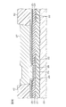
- FIG. 1 is a cross-sectional view showing a configuration of a semiconductor device according to an embodiment of the present invention.
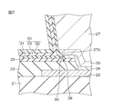
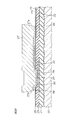
- FIG. 2 is a partially enlarged cross-sectional view showing an enlarged structure near the lower edge of the upper wiring (uppermost layer wiring).
- 3A is a schematic cross-sectional view in the manufacturing process of the semiconductor device shown in FIG. 1 and FIG.
- FIG. 3B is a schematic cross-sectional view in the next step of FIG. 3A.
- FIG. 3C is a schematic cross-sectional view in the next step of FIG. 3B.
- FIG. 3D is a schematic cross-sectional view in the next step of FIG. 3C.
- FIG. 3E is a schematic cross-sectional view in the next step of FIG. 3D.
- FIG. 3F is a schematic cross-sectional view in the next step of FIG. 3E.
- FIG. 3G is a schematic cross-sectional view in the next step of FIG. 3F.
- FIG. 3H is a schematic cross-sectional view in the next step of FIG. 3G.
- FIG. 3I is a schematic cross-sectional view in the next step of FIG. 3H.
- FIG. 3J is a schematic cross-sectional view in the next step of FIG. 3I.
- FIG. 3K is a schematic cross-sectional view in the next step of FIG. 3J.
- 3L is a schematic cross-sectional view in the next step of FIG. 3K.
- FIG. 4A is an electron micrograph of a semiconductor device (Example) manufactured according to the embodiment.
- FIG. 4A is an electron micrograph of a semiconductor device (Example) manufactured according to the embodiment.
- FIG. 4A is an electron micrograph of a semiconductor device (Example) manufactured according to the embodiment.
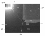
- FIG. 4B is an electron micrograph of a comparative example in which a passivation film is formed of a single layer of SiN having a thickness of 2 ⁇ m.
- FIG. 5 is a cross-sectional view showing a configuration of a semiconductor device according to another embodiment of the present invention. It is sectional drawing which shows the structure of the trial example (comparative example) which covered the thick film copper wiring with the single layer silicon nitride film.
- FIG. 1 is a cross-sectional view showing a configuration of a semiconductor device according to an embodiment of the present invention.
- the semiconductor device 10 includes a semiconductor substrate 20.
- the semiconductor substrate 20 is, for example, a Si (silicon) substrate.
- a transistor for example, a power transistor
- other functional elements are built in the semiconductor substrate 20.
- a first interlayer insulating film 21 is stacked on the semiconductor substrate 20.
- the first interlayer insulating film 21 is made of, for example, SiO 2 (silicon oxide).
- a lower wiring 22 is formed on the first interlayer insulating film 21.
- the lower wiring 22 is made of, for example, aluminum or an aluminum alloy.
- a second interlayer insulating film 23 is stacked on the first interlayer insulating film 21 and the lower wiring 22.
- the second interlayer insulating film 23 is made of, for example, SiO 2 .
- the surface of the second interlayer insulating film 23 is planarized.
- a third interlayer insulating film 25 is stacked on the second interlayer insulating film 23.
- the third interlayer insulating film 25 is made of, for example, SiN (silicon nitride).
- via holes 26 penetrating in the thickness direction are formed in portions facing the lower wiring 22 in the thickness direction.
- the via hole 26 is formed in a tapered shape such that the opening area increases toward the upper side.
- an upper wiring 27 as the uppermost layer wiring is formed on the third interlayer insulating film 25, an upper wiring 27 as the uppermost layer wiring is formed.
- the upper wiring 27 is formed on a region including the via hole 26 in plan view, and is formed to protrude upward from the third interlayer insulating film 25.
- the upper wiring 27 has a thickness such that the protruding amount from the surface of the third interlayer insulating film 25 is 2 ⁇ m or more (for example, 10 ⁇ m to 20 ⁇ m).
- the lower end portion of the upper wiring 27 enters the via hole 26 and is connected to the lower wiring 22.
- the upper wiring 27 is made of Cu (for example, Cu having a purity of 99.9%).
- the barrier film 28 is made of, for example, Ti (titanium) or TiW (titanium-tungsten alloy).
- the barrier film 28 can prevent Cu (Cu ions) from diffusing from the upper wiring 27, thereby preventing a leak path from being formed between the upper wiring 27 and another uppermost wiring.
- a passivation film 30 is formed on the third interlayer insulating film 25 and the upper wiring 27.
- the passivation film 30 is formed so as to cover the surface (top surface and side surface) of the upper wiring 27.
- a recess corresponding to the via hole 26 is formed immediately above the via hole 26.
- a pad opening 34 exposing a part of the surface of the upper wiring 27 is formed in a flat region shifted from the depression so as to penetrate in the thickness direction of the passivation film 30.
- a portion of the upper wiring 27 exposed from the pad opening 34 is a pad.
- a cap metal layer 35 is formed in contact with the pad.
- the cap metal layer 35 is formed in a region covering the pad opening 34, fills up the pad opening 34, and is in contact with the upper wiring 27.
- the cap metal layer 35 is made of, for example, a laminated film of a barrier layer 35a and an adhesive layer 35b.
- the barrier layer 35 a is in contact with the upper wiring 27 at the pad opening 34.
- the barrier layer 35a has a barrier property against diffusion of Cu ions and Au, and is made of, for example, Ti (titanium) or TiW (titanium tungsten).
- the adhesive layer 35b is made of, for example, aluminum or an aluminum alloy.
- One end of a bonding wire 36 made of Au is bonded to the cap metal layer 35.
- the other end of the bonding wire 36 is connected to the outside of the semiconductor device 10.
- the bonding wire 36 is electrically connected to the lower wiring 22 through the cap metal layer 35, the upper wiring 27 and the barrier film 28.
- the barrier layer 35 a included in the cap metal layer 35 prevents Au in the bonding wire 36 from diffusing into the upper wiring 27, and prevents Cu in the upper wiring 27 from diffusing into the bonding wire 36.
- the adhesive layer 35b included in the cap metal layer 35 has good adhesion to the barrier layer 35a and excellent adhesion to the bonding wire 36 made of Au.
- the passivation film 30 is formed of a laminated film in which a first nitride film 31, a second nitride film 32, and an intermediate film 33 are laminated.
- the lowermost first nitride film 31 is in contact with the top surface and the side surface of the upper wiring 27, and is further in contact with the surface of the third interlayer insulating film 25.
- the intermediate film 33 is sandwiched between the first nitride film 31 and the second nitride film 32.
- the uppermost second nitride film 32 is exposed to the outside, and is in contact with the cap metal layer 35 from below (semiconductor substrate 20 side) at the periphery of the pad opening 34.
- the first nitride film 31 and the second nitride film 32 are made of, for example, SiN (silicon nitride).
- the thickness of the first nitride film 31 is preferably 0.1 ⁇ m to 0.5 ⁇ m (for example, 0.5 ⁇ m).
- the thickness of the second nitride film 32 is preferably 0.8 ⁇ m to 2.0 ⁇ m (for example, 1.0 ⁇ m).
- the intermediate film 33 is made of an oxide film such as SiO 2 (silicon oxide).
- the film thickness of the intermediate film 33 is preferably 0.2 ⁇ m to 1.0 ⁇ m (for example, 0.5 ⁇ m).
- the intermediate film 33 is preferably made of a material having a stress smaller than that of the first nitride film 31 and the second nitride film 32.
- the stress of SiN is 0.2 GPa while the stress of SiO 2 is 0.1 GPa.
- the thickness of the intermediate film 33 is preferably set to a value sufficient to alleviate the stress generated in the first nitride film 31.
- FIG. 2 is a partially enlarged cross-sectional view showing the structure near the lower edge of the upper wiring 27 in an enlarged manner.
- the barrier film 28 is patterned by wet etching using the upper wiring 27 as a mask. Therefore, the barrier film 28 is over-etched near the edge of the upper wiring 27. That is, the edge portion of the barrier film 28 recedes inward in the region below the upper wiring 27 rather than the lower edge portion of the upper wiring 27. That is, the upper wiring 27 has an overhang portion 27 a protruding from the edge of the barrier film 28 in the vicinity of the lower edge.
- An over-etching region 38 having a U-shaped cross section (laterally U-shaped) is formed below the overhang portion 27a.
- the first nitride film 31 of the passivation film 30 enters the overetching region 38 and is in contact with the surface of each film that partitions the region 38. That is, the first nitride film 31 is attached to the surface of the third interlayer insulating film 25, the side wall surface of the barrier film 28, and the bottom surface of the upper wiring 27. Since film formation with such a complicated structure is difficult, the air gap 39 may be generated in the first nitride film 31 in some cases. When a large stress is generated in the first nitride film 31, a crack with the gap 39 as a base point is likely to occur. Therefore, in this embodiment, the intermediate film 33 is laminated on the first nitride film 31.
- the passivation film 30 since the stress of the 1st nitride film 31 is relieved, generation
- FIGS. 3A to 3L are schematic cross-sectional views in each manufacturing process of the semiconductor device shown in FIGS.
- a first interlayer insulating film 21 is laminated on the surface of a semiconductor substrate 20 in which a transistor and other functional elements are formed by a CVD (Chemical Vapor Deposition) method.
- an Al film serving as a material for the lower wiring 22 is formed on the first interlayer insulating film 21 by sputtering.
- the lower wiring 22 is formed by patterning the Al film by photolithography and etching.
- an oxide film (SiO 2 film) 23a is formed on the first interlayer insulating film 21 and the lower wiring 22 by HDP (High Density Plasma) CVD.
- HDP High Density Plasma
- a USG (Undoped Silicate Glass) film 23b is formed on the oxide film 23a by plasma CVD.
- a second interlayer insulating film 23 composed of a laminated film of the oxide film 23a and the USG film 23b is formed.
- the second interlayer insulating film 23 is ground from its surface by a CMP (Chemical Mechanical Polishing) method.
- the grinding of the second interlayer insulating film 23 is performed so that the film thickness of the second interlayer insulating film 23 becomes a predetermined target value (for example, 9500 mm).
- a predetermined target value for example, 9500 mm.
- the surface of the second interlayer insulating film 23 is planarized.
- a third interlayer insulating film 25 is formed on the second interlayer insulating film 23 by plasma CVD.
- a resist mask 41 having a pattern having an opening on the lower wiring 22 is formed on the third insulating film 25.
- the third interlayer insulating film 25 and the second interlayer insulating film 23 are selectively removed by dry etching (for example, RIE: reactive ion etching) using the resist mask 41 as a mask, A via hole 26 penetrating them in the thickness direction is formed.
- a barrier film 28 made of, for example, TiW is formed on the inner surface (bottom surface and side wall) of the via hole 26 and the third interlayer insulating film 25 by sputtering.
- a seed film 29 made of Cu is formed on the barrier film 28 by sputtering.
- a resist pattern 42 having an opening in a portion facing the region including the via hole 26 in plan view is formed on the barrier film 28 and the seed film 29.
- the opening of the resist pattern 42 is formed in a pattern corresponding to the wiring pattern of the upper wiring 27.
- Cu is plated and grown in the opening of the resist pattern 42.
- the opening of the resist pattern 42 is completely filled with Cu, and the upper wiring 27 of a predetermined wiring pattern made of Cu is formed.
- the resist pattern 42 is removed.
- the upper wiring 27 has a film thickness of about 10 ⁇ m and a width of about 10 ⁇ m. That is, the upper wiring 27 is formed in a state protruding from the third interlayer insulating film 25 by about 10 ⁇ m.
- the seed film 29 and the barrier film 28 are sequentially etched by wet etching using the upper wiring 27 as a mask. As a result, portions of the seed film 29 and the barrier film 28 that have been formed below the resist pattern 42 are removed. As a result, the seed film 29 and the barrier film 28 are etched into a wiring pattern that matches the upper wiring 27. During the wet etching, the over-etching of the barrier film 28 occurs, whereby the overhang portion 27a and the over-etching region 38 described above are formed.
- the substrate 20 is carried into the processing chamber 50 of the plasma CVD apparatus, and the upper wiring 27 is subjected to plasma processing with a reducing gas in the processing chamber 50.
- the reducing gas is a gas having a property of reducing and removing oxide on the surface of the upper wiring 27.
- Examples of such reducing gas include H 2 (hydrogen) gas and NH 3 (ammonia) gas.
- An NH 3 / H 2 mixed gas may be used as the reducing gas.
- Such reducing gas is supplied to the processing chamber 50, and plasma of the reducing gas is generated in the processing chamber 50.
- the oxide film on the surface of the upper wiring 27 is removed by the plasma treatment using the reducing gas.
- a passivation film 30 is formed in the same processing chamber 50 by plasma CVD.
- the first nitride film 31 is formed, then the intermediate film 33 is formed on the first nitride film 31, and then the second nitride film 32 is formed on the intermediate film 33.
- the first nitride film 31 and the second nitride film 32 are formed by, for example, a plasma CVD method in which SiH 4 (silane), N 2 (nitrogen), and NH 3 (ammonia) are supplied to the processing chamber 50 as source gases. The Thereby, a SiN film is formed.
- the intermediate film 33 is formed by, for example, a plasma CVD method in which SiH 4 (silane), N 2 O (nitrous oxide), and O 2 (oxygen) are supplied to the processing chamber 50 as source gases. Thereby, a SiO 2 film is formed.
- the substrate temperature during film formation is, for example, 300 ° C. to 400 ° C.
- the first nitride film 31 adheres well to the upper wiring 27.
- the first nitride film 31 is formed so as to cover the top surface and side surfaces of the upper wiring 27 and the surface of the third interlayer insulating film 25.
- the first nitride film 31 covers the third interlayer insulating film 25 at least in a region near the side surface of the upper wiring 27.
- the intermediate film 33 is formed so as to cover the first nitride film 31.
- the second nitride film 32 is formed so as to cover the intermediate film 33.
- a resist mask 43 having openings corresponding to the pad openings 34 is formed.
- dry etching for example, RIE
- a pad opening 34 is formed in the passivation film 30 and a part of the upper wiring 27 is exposed.
- the resist mask 43 is peeled off, the state shown in FIG. 3J is obtained.
- a barrier layer 35a and an adhesive layer 35b are formed in this order on the third interlayer insulating film 25 and the upper wiring 27 by sputtering. Then, a resist mask 44 corresponding to the cap metal layer 35 is formed above the pad opening 34.
- the barrier layer 35a is made of, for example, a TiW film having a thickness of 500 mm.
- the adhesive layer 35b is made of, for example, an Al film having a thickness of 1000 mm.
- the adhesive layer 35b is patterned by dry etching (for example, RIE) using the resist mask 44 as a mask. Further, the barrier layer 35a is patterned by wet etching using the patterned adhesive layer 35b as a mask. Thus, a cap metal layer 35 covering the pad opening 34 is formed. Thereafter, one end of the bonding wire 36 is joined to the cap metal layer 35, whereby the semiconductor device 10 shown in FIG. 1 is obtained.
- dry etching for example, RIE
- the barrier layer 35a is patterned by wet etching using the patterned adhesive layer 35b as a mask.
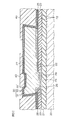
- FIG. 4A is an electron micrograph of the semiconductor device manufactured according to the embodiment, and shows the lower edge portion of the upper wiring 27.
- the first nitride film 31 is made of SiN and has a film thickness of 0.5 ⁇ m.
- the intermediate film 33 is made of SiO 2 and has a film thickness of 0.5 ⁇ m.
- the second nitride film 32 is made of SiN and has a thickness of 1.0 ⁇ m.
- a gap 39 is formed in the vicinity of the overetching region 38, but defects such as cracks are generated in any of the first nitride film 31, the second nitride film 32, and the intermediate film 33. Absent. Therefore, the passivation film 30 as a whole has good protection performance.
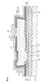
- FIG. 4B is an electron micrograph of a comparative example in which the passivation film 5 is formed of a single layer of SiN having a thickness of 2 ⁇ m.
- the passivation film 5 is formed of a single layer of SiN having a thickness of 2 ⁇ m.
- a crack 7 is generated due to the gap 6 generated in the vicinity of the overetching region 38. Therefore, there is a concern of intrusion of moisture or the like from the outside, and it does not have sufficient protection performance.
- the passivation film 30 covering the upper wiring 27 (uppermost layer wiring) formed so as to protrude from the surface of the third interlayer insulating film 25 includes the first nitride film 31 and It consists of a laminated film with the intermediate film 33 sandwiched between the second nitride films 32.
- the intermediate film 33 is made of an oxide film that is made of a material different from that of the first nitride film 31 and has a lower stress than the nitride film. Therefore, since the intermediate film 33 functions as a buffer film that relieves the stress of the first nitride film 31, the passivation film 30 having a sufficient film thickness as a whole is realized while suppressing cracks in the first nitride film 31. it can. Thereby, the upper wiring 27 made of Cu can be protected. In addition, since the first nitride film 31 without cracks is in contact with the upper wiring 27, copper diffusion from the upper wiring 27 can be prevented.
- the passivation film 30 has a sufficient thickness as a whole. Therefore, by reducing the thickness of the first nitride film 31, the stress of the first nitride film 31 can be further reduced. Particularly, the stress of the first nitride film 31 is reduced by making the film thickness of the first nitride film 31 smaller than the film thickness of the second nitride film 32, while the second nitride film 32 having a large film thickness is used for passivation. The protection performance of the film 30 can be enhanced.
- the upper wiring 27 is formed by plating
- plasma processing with a reducing gas is performed in the processing chamber 50
- the first nitride film 31 is formed by plasma CVD in the same processing chamber 50. Is formed.
- the oxide film on the surface of the upper wiring 27 is removed immediately before the formation of the first nitride film 31, so that the first nitride film 31 has excellent adhesion to the upper wiring 27.
- peeling of the passivation film 30 can be prevented, so that the highly reliable semiconductor device 10 can be provided.
- FIG. 5 is a cross-sectional view showing a configuration of a semiconductor device according to another embodiment of the present invention.
- the intermediate film 33 of the passivation film 30 has a taper-shaped cross-sectional profile (contour) that becomes narrower toward the upper side (the direction away from the semiconductor substrate 20).
- the film thickness of the intermediate film 33 can be increased at the periphery of the contact portion between the upper wiring 27 and the third interlayer insulating film 25. Therefore, the stress concentration of the first nitride film 31 can be more effectively alleviated in the vicinity of the overetching region 38. As a result, the occurrence of cracks in the first nitride film 31 can be more effectively suppressed.
- the surface shape of the intermediate film 33 exhibits a gradual change.
- the surface of the intermediate film 33 has a trapezoidal outline in which the long side and the side side form an obtuse angle in the cross section.
- the second nitride film 32 formed on the intermediate film 33 is in close contact with the intermediate film 33 with good coverage (coverability).
- the protection performance of the passivation film 30 can be further improved.
- the intermediate film 33 as described above can be formed by, for example, a high-density plasma CVD (HDPCVD: High-Density Plasma Chemical Vapor Deposition) method. More specifically, in the process of FIG. 3H (passivation film formation process) described above, the first nitride film 31 is formed by the plasma CVD method, the intermediate film 33 is formed by the HDPCVD method, and then the second film is formed.
- the nitride film 32 may be formed by a plasma CVD method. As a result, the intermediate film 33 has a trapezoidal profile.
- the intermediate film 33 of the passivation film 30 is made of SiO 2
- the intermediate film 33 may be made of SiON (silicon oxynitride).
- SiN is exemplified as the material of the third interlayer insulating film 25.
- SiO 2 may be used instead.
- Cu ions are more easily diffused in SiO 2 than in SiN, the use of SiN as the material of the third interlayer insulating film 25 can more effectively prevent Cu ions from diffusing.
- Ti and TiW are exemplified as the material of the barrier film 28 and the barrier layer 35a.
- the barrier film 28 and the barrier layer 35a are conductive and have other barrier properties against diffusion of Cu ions and Au. May be formed. Examples of such materials include TiN (titanium nitride), WN (tungsten nitride), TaN (tantalum nitride), Ta (tantalum), and W (tungsten) in addition to Ti and TiW.
- Al is exemplified as the material of the adhesive layer 35b of the cap metal layer 35
- any metal material having high adhesion to Cu and an insulating material may be used.
- Al for example, AlSiCu (aluminum-copper alloy) Silicon compound) or AlCu (aluminum-copper alloy) can also be applied.
Landscapes
- Internal Circuitry In Semiconductor Integrated Circuit Devices (AREA)
- Engineering & Computer Science (AREA)
- Manufacturing & Machinery (AREA)
Abstract
Description
この発明の目的は、上記課題を克服した半導体装置およびその製造方法を提供することである。
前記銅配線は厚みが10μm以上(たとえば10μm~20μm)であってもよい。このような厚膜銅配線を前述のようなパッシベーション膜で覆うことによって、厚膜銅配線と層間絶縁膜との接触部近傍などでパッシベーション膜にクラックが生じることを抑制して、厚膜銅配線を充分に保護することができる。また、前記銅配線は幅が10μm以上(たとえば10μm~20μm)であってもよい。たとえば、このような幅広(好ましくはさらに厚膜)の銅配線は、パワーデバイスの電源配線であってもよい。また、前記銅配線は、最上層配線であってもよい。
前記中間膜は、前記第1窒化膜の材料よりも応力の小さい材料からなるバッファ(緩衝)膜であることが好ましい。この構成により、第1窒化膜に生じる応力を効果的に緩和できる。
この発明の一実施形態においては、前記半導体装置は、前記層間絶縁膜上に形成され、前記配線中の銅が前記層間絶縁膜へと拡散することを防ぐバリア膜をさらに含む。そして、前記配線が、前記バリア膜上に形成され、前記バリア膜の縁部から張り出したオーバーハング部を有している。このようなオーバーハング部は、たとえば、銅配線をマスクとしてバリア膜をウェットエッチングする場合に、不可避的に生じる。第1窒化膜を形成すると、オーバーハング部と層間絶縁膜との間の隙間に第1窒化膜が入り込む。この隙間の部分では、第1窒化膜が、層間絶縁膜、バリア膜の側壁、および銅配線の底面に付着し、その結果、第1窒化膜中に空隙が生じる場合がある。第1窒化膜に大きな応力が生じると、当該空隙を基点としたクラックが生じやすくなる。この発明の構成では、第1窒化膜に中間膜が積層されることによってその応力が緩和されるので、クラックの発生を抑制できる。
前記中間膜は、前記配線の厚さ方向に沿って前記層間絶縁膜から離れるほど幅狭となるテーパー部を有していてもよい。この構成によれば、配線と層間絶縁膜との接触部の周縁において中間膜の膜厚を厚くできるから、第1窒化膜の応力集中をより一層効果的に緩和できる。これにより、クラックの発生を一層効果的に抑制できる。また、中間膜に対する第2窒化膜のカバレッジが良くなるから、パッシベーション膜の保護性能を高くすることができる。
この発明の半導体装置の製造方法は、層間絶縁膜上に突出するように、銅を主成分とする材料からなる配線を形成する工程と、処理室内で、還元性ガスによるプラズマ処理を前記配線に施す工程と、前記プラズマ処理の後、前記処理室内で、プラズマCVD法によって前記配線の表面(頂面および側面を含む。)および層間絶縁膜の表面(少なくとも前記配線の側面近傍領域の表面)を覆う第1窒化膜を形成する工程と、前記第1窒化膜を覆うように、前記第1窒化膜とは異なる材料からなる中間膜を形成する工程と、前記中間膜を覆うように、前記中間膜とは異なる材料からなる第2窒化膜を形成する工程とを含む。
前記配線を形成する工程は、前記層間絶縁膜上にバリア膜を形成する工程と、前記バリ膜上に所定の配線パターンの銅膜を形成する工程と、前記バリア膜を前記配線パターンにエッチング(たとえばウェットエッチング)する工程とを含んでいてもよい。バリア膜のエッチング(とくにウェットエッチング)によって、前述のようなオーバーハング部が生じる。この場合でも、第1窒化膜のクラックを効果的に抑制できることは既述のとおりである。
前記中間膜を形成する工程は、高密度プラズマCVD(High-Density Plasma Chemical Vapor Deposition)法によって酸化膜を形成する工程を含んでいてもよい。この場合、中間膜は、テーパー形状の断面プロファイルを有することになる。これにより、銅配線と層間絶縁膜との接触部における中間膜の膜厚が厚くなるので、第1窒化膜の応力を一層効果的に低減できる。加えて、中間膜に対する第2窒化膜のカバレッジが良くなるので、パッシベーション膜の性能を向上できる。
第2層間絶縁膜23上には、第3層間絶縁膜25が積層されている。第3層間絶縁膜25は、たとえば、SiN(窒化シリコン)からなる。
第3層間絶縁膜25上には、最上層配線としての上配線27が形成されている。
上配線27は、平面視でビアホール26を含む領域上に形成され、第3層間絶縁膜25から上方に突出して形成されている。上配線27は、たとえば、第3層間絶縁膜25の表面からの突出量が2μm以上(たとえば、10μm~20μm)となるような厚さを有している。上配線27の下端部は、ビアホール26内に入り込み、下配線22に接続されている。上配線27は、Cu(たとえば、純度99.9%のCu)からなる。
中間膜33は、たとえば、SiO2(酸化シリコン)等の酸化膜からなる。中間膜33の膜厚は、0.2μm~1.0μm(たとえば0.5μm)とすることが好ましい。中間膜33は、第1窒化膜31および第2窒化膜32の材料よりも応力の小さい材料で構成するとよい。たとえば、SiNの応力は0.2GPaであるのに対して、SiO2の応力は0.1GPaである。また、中間膜33の膜厚は、とくに第1窒化膜31に生じる応力を緩和するのに充分な値とすることが好ましい。
図3Aに示すように、トランジスタその他の機能素子が作り込まれた半導体基板20の表面に、CVD(Chemical Vapor Deposition:化学的気相成長)法により、第1層間絶縁膜21が積層される。その後、スパッタ法により、第1層間絶縁膜21上に、下配線22の材料となるAl膜が形成される。そして、フォトリソグラフィおよびエッチングにより、Al膜がパターニングされることにより、下配線22が形成される。次いで、HDP(High Density Plasma:高密度プラズマ)CVD法により、第1層間絶縁膜21および下配線22上に、酸化膜(SiO2膜)23aが形成される。その後、プラズマCVD法により、酸化膜23a上に、USG(Undoped Silicate Glass)膜23bが形成される。これにより、酸化膜23aおよびUSG膜23bの積層膜からなる第2層間絶縁膜23が形成される。
次に、図3Dに示すように、スパッタ法により、ビアホール26の内面(底面および側壁)および第3層間絶縁膜25上に、たとえばTiWからなるバリア膜28が形成される。続いて、スパッタ法により、バリア膜28上に、Cuからなるシード膜29が形成される。
以上のように、この実施形態の半導体装置10においては、第3層間絶縁膜25の表面から突出して形成された上配線27(最上層配線)を覆うパッシベーション膜30が、第1窒化膜31および第2窒化膜32の間に中間膜33を挟んだ積層膜からなる。そして、中間膜33は、第1窒化膜31とは異なる材料であり、窒化膜よりも応力の小さい酸化膜からなっている。これにより、中間膜33は、第1窒化膜31の応力を緩和するバッファ膜として機能するから、第1窒化膜31のクラックを抑制しつつ、全体として充分な膜厚を有するパッシベーション膜30を実現できる。これにより、Cuからなる上配線27を保護できる。また、クラックのない第1窒化膜31が上配線27に接しているので、上配線27からの銅の拡散を阻止できる。
また、前述の実施形態では、第3層間絶縁膜25の材料として、SiNを例示したが、代わりにSiO2を用いてもよい。ただし、Cuイオンは、SiN中よりもSiO2中の方が拡散しやすいので、第3層間絶縁膜25の材料としてSiNを用いることにより、Cuイオンの拡散をより良好に防止することができる。
本発明の実施形態について詳細に説明してきたが、これらは本発明の技術的内容を明らかにするために用いられた具体例に過ぎず、本発明はこれらの具体例に限定して解釈されるべきではなく、本発明の範囲は添付の請求の範囲によってのみ限定される。
20 半導体基板
21 第1層間絶縁膜
22 下配線
23 第2層間絶縁膜
25 第3層間絶縁膜
27 上配線
27a オーバーハング部
28 バリア膜
29 シード膜
30 パッシベーション膜
31 第1窒化膜
32 第2窒化膜
33 中間膜
34 パッド開口
35 キャップメタル層
36 ボンディングワイヤ
38 オーバーエッチング領域
39 空隙
50 処理室
Claims (10)
- 層間絶縁膜と、
前記層間絶縁膜上に突出して形成され、銅を主成分とする材料からなる配線と、
前記配線を覆うように形成されたパッシベーション膜とを含み、
前記パッシベーション膜が、前記配線側から順に第1窒化膜、中間膜および第2窒化膜を積層した積層膜からなり、前記中間膜が、前記第1および第2窒化膜とは異なる絶縁材料からなる、半導体装置。 - 前記中間膜は、前記第1窒化膜の材料よりも応力の小さい材料からなるバッファ膜である、請求項1記載の半導体装置。
- 前記層間絶縁膜上に形成され、前記配線中の銅が前記層間絶縁膜へと拡散することを防ぐバリア膜をさらに含み、
前記配線が、前記バリア膜上に形成され、前記バリア膜の縁部から張り出したオーバーハング部を有している、請求項1または2記載の半導体装置。 - 前記第1窒化膜の膜厚が、前記第2窒化膜の膜厚よりも小さい、請求項1~3のいずれか一項に記載の半導体装置。
- 前記中間膜が、前記配線の厚さ方向に沿って前記層間絶縁膜から離れるほど幅狭となるテーパー部を有している、請求項1~4のいずれか一項に記載の半導体装置。
- 層間絶縁膜上に突出するように、銅を主成分とする材料からなる配線を形成する工程と、
処理室内で、還元性ガスによるプラズマ処理を前記配線に施す工程と、
前記プラズマ処理の後、前記処理室内で、プラズマCVD法によって前記配線の表面および前記層間絶縁膜の表面を覆う第1窒化膜を形成する工程と、
前記第1窒化膜を覆うように、前記第1窒化膜とは異なる材料からなる中間膜を形成する工程と、
前記中間膜を覆うように、前記中間膜とは異なる材料からなる第2窒化膜を形成する工程とを含む、半導体装置の製造方法。 - 前記中間膜を形成する工程は、前記第1窒化膜の材料よりも応力の小さい材料からなるバッファ膜を形成する工程を含む、請求項6記載の半導体装置の製造方法。
- 前記配線を形成する工程は、前記層間絶縁膜上にバリア膜を形成する工程と、前記バリア膜上に所定の配線パターンの銅膜を形成する工程と、前記バリア膜を前記配線パターンにエッチングする工程とを含む、請求項6または7記載の半導体装置の製造方法。
- 前記第1窒化膜の膜厚が前記第2窒化膜の膜厚よりも小さくなるように、前記第1および第2窒化膜が形成される、請求項6~8のいずれか一項に記載の半導体装置の製造方法。
- 前記中間膜を形成する工程が、高密度プラズマCVD法によって酸化膜を形成する工程を含む、請求項6~9のいずれか一項に記載の半導体装置の製造方法。
Priority Applications (2)
| Application Number | Priority Date | Filing Date | Title |
|---|---|---|---|
| US13/634,212 US9425147B2 (en) | 2010-04-01 | 2011-04-01 | Semiconductor device |
| CN2011800158128A CN102822958A (zh) | 2010-04-01 | 2011-04-01 | 半导体装置及其制造方法 |
Applications Claiming Priority (2)
| Application Number | Priority Date | Filing Date | Title |
|---|---|---|---|
| JP2010-085193 | 2010-04-01 | ||
| JP2010085193A JP2011216771A (ja) | 2010-04-01 | 2010-04-01 | 半導体装置およびその製造方法 |
Publications (1)
| Publication Number | Publication Date |
|---|---|
| WO2011125928A1 true WO2011125928A1 (ja) | 2011-10-13 |
Family
ID=44762866
Family Applications (1)
| Application Number | Title | Priority Date | Filing Date |
|---|---|---|---|
| PCT/JP2011/058400 Ceased WO2011125928A1 (ja) | 2010-04-01 | 2011-04-01 | 半導体装置およびその製造方法 |
Country Status (4)
| Country | Link |
|---|---|
| US (1) | US9425147B2 (ja) |
| JP (1) | JP2011216771A (ja) |
| CN (1) | CN102822958A (ja) |
| WO (1) | WO2011125928A1 (ja) |
Cited By (4)
| Publication number | Priority date | Publication date | Assignee | Title |
|---|---|---|---|---|
| WO2014055315A1 (en) * | 2012-10-04 | 2014-04-10 | Cree, Inc. | Hydrogen mitigation schemes in the passivation of advanced devices |
| JP2016115892A (ja) * | 2014-12-17 | 2016-06-23 | ルネサスエレクトロニクス株式会社 | 半導体装置およびその製造方法 |
| US9812338B2 (en) | 2013-03-14 | 2017-11-07 | Cree, Inc. | Encapsulation of advanced devices using novel PECVD and ALD schemes |
| US9991399B2 (en) | 2012-10-04 | 2018-06-05 | Cree, Inc. | Passivation structure for semiconductor devices |
Families Citing this family (13)
| Publication number | Priority date | Publication date | Assignee | Title |
|---|---|---|---|---|
| US20140264865A1 (en) * | 2013-03-14 | 2014-09-18 | Infineon Technologies Ag | Semiconductor device and manufacturing method thereof |
| JP2016174021A (ja) * | 2015-03-16 | 2016-09-29 | 株式会社東芝 | 半導体装置 |
| JP6484490B2 (ja) * | 2015-04-10 | 2019-03-13 | ルネサスエレクトロニクス株式会社 | 半導体装置およびその製造方法 |
| JP6502751B2 (ja) * | 2015-05-29 | 2019-04-17 | 東芝メモリ株式会社 | 半導体装置および半導体装置の製造方法 |
| JP2017033984A (ja) * | 2015-07-29 | 2017-02-09 | セイコーエプソン株式会社 | 半導体装置及びその製造方法、並びに、電子機器 |
| CN105633047B (zh) * | 2016-03-10 | 2018-07-06 | 三星半导体(中国)研究开发有限公司 | 半导体封装件及其制造方法 |
| JP2018064059A (ja) * | 2016-10-14 | 2018-04-19 | 株式会社デンソー | 半導体装置 |
| CN109494214B (zh) * | 2017-09-11 | 2021-05-04 | 联华电子股份有限公司 | 半导体装置的连接结构以及其制作方法 |
| JP7172105B2 (ja) * | 2018-04-09 | 2022-11-16 | 大日本印刷株式会社 | 配線基板、配線基板を有する半導体装置、および半導体装置の作製方法 |
| JP7181699B2 (ja) * | 2018-04-10 | 2022-12-01 | ローム株式会社 | 半導体レーザ装置 |
| US11756832B2 (en) * | 2019-09-30 | 2023-09-12 | Taiwan Semiconductor Manufacturing Company, Ltd. | Gate structures in semiconductor devices |
| DE102020100099B4 (de) | 2019-09-30 | 2025-09-11 | Taiwan Semiconductor Manufacturing Co., Ltd. | Gatestrukturen in halbleitervorrichtungen und deren herstellung |
| US20220157655A1 (en) * | 2020-11-19 | 2022-05-19 | Applied Materials, Inc. | Electroplating with temporary features |
Citations (6)
| Publication number | Priority date | Publication date | Assignee | Title |
|---|---|---|---|---|
| JPH05144811A (ja) * | 1991-11-22 | 1993-06-11 | Hitachi Ltd | 薄膜半導体装置及びその製造方法 |
| JPH0689893A (ja) * | 1991-11-11 | 1994-03-29 | Nec Corp | 半導体装置 |
| JPH09120963A (ja) * | 1995-08-23 | 1997-05-06 | Internatl Business Mach Corp <Ibm> | 半導体デバイス用の平坦化最終パッシベーション |
| WO2000044043A1 (fr) * | 1999-01-22 | 2000-07-27 | Hitachi, Ltd. | Dispositif a semi-conducteurs et son procede de fabrication |
| JP2008066450A (ja) * | 2006-09-06 | 2008-03-21 | Rohm Co Ltd | 半導体装置 |
| JP2008091454A (ja) * | 2006-09-29 | 2008-04-17 | Rohm Co Ltd | 半導体装置及び半導体装置の製造方法 |
Family Cites Families (8)
| Publication number | Priority date | Publication date | Assignee | Title |
|---|---|---|---|---|
| US6060378A (en) * | 1995-11-03 | 2000-05-09 | Micron Technology, Inc. | Semiconductor bonding pad for better reliability |
| EP1139413B1 (en) | 2000-03-24 | 2005-03-16 | Texas Instruments Incorporated | Wire bonding process |
| US6362531B1 (en) * | 2000-05-04 | 2002-03-26 | International Business Machines Corporation | Recessed bond pad |
| DE102004005645B4 (de) * | 2004-02-04 | 2006-01-12 | Infineon Technologies Ag | Verfahren zur Herstellung von Schichtaufbauten zur Signalverteilung |
| US7316971B2 (en) * | 2004-09-14 | 2008-01-08 | International Business Machines Corporation | Wire bond pads |
| US8420520B2 (en) * | 2006-05-18 | 2013-04-16 | Megica Corporation | Non-cyanide gold electroplating for fine-line gold traces and gold pads |
| US7601628B2 (en) * | 2006-11-20 | 2009-10-13 | International Business Machines Corporation | Wire and solder bond forming methods |
| KR100893939B1 (ko) * | 2007-02-16 | 2009-04-21 | 삼성전자주식회사 | 본딩 패드 구조체를 갖는 전자 장치 및 그 제조방법 |
-
2010
- 2010-04-01 JP JP2010085193A patent/JP2011216771A/ja active Pending
-
2011
- 2011-04-01 WO PCT/JP2011/058400 patent/WO2011125928A1/ja not_active Ceased
- 2011-04-01 US US13/634,212 patent/US9425147B2/en active Active
- 2011-04-01 CN CN2011800158128A patent/CN102822958A/zh active Pending
Patent Citations (6)
| Publication number | Priority date | Publication date | Assignee | Title |
|---|---|---|---|---|
| JPH0689893A (ja) * | 1991-11-11 | 1994-03-29 | Nec Corp | 半導体装置 |
| JPH05144811A (ja) * | 1991-11-22 | 1993-06-11 | Hitachi Ltd | 薄膜半導体装置及びその製造方法 |
| JPH09120963A (ja) * | 1995-08-23 | 1997-05-06 | Internatl Business Mach Corp <Ibm> | 半導体デバイス用の平坦化最終パッシベーション |
| WO2000044043A1 (fr) * | 1999-01-22 | 2000-07-27 | Hitachi, Ltd. | Dispositif a semi-conducteurs et son procede de fabrication |
| JP2008066450A (ja) * | 2006-09-06 | 2008-03-21 | Rohm Co Ltd | 半導体装置 |
| JP2008091454A (ja) * | 2006-09-29 | 2008-04-17 | Rohm Co Ltd | 半導体装置及び半導体装置の製造方法 |
Cited By (6)
| Publication number | Priority date | Publication date | Assignee | Title |
|---|---|---|---|---|
| WO2014055315A1 (en) * | 2012-10-04 | 2014-04-10 | Cree, Inc. | Hydrogen mitigation schemes in the passivation of advanced devices |
| US8994073B2 (en) | 2012-10-04 | 2015-03-31 | Cree, Inc. | Hydrogen mitigation schemes in the passivation of advanced devices |
| US9991399B2 (en) | 2012-10-04 | 2018-06-05 | Cree, Inc. | Passivation structure for semiconductor devices |
| USRE49167E1 (en) | 2012-10-04 | 2022-08-09 | Wolfspeed, Inc. | Passivation structure for semiconductor devices |
| US9812338B2 (en) | 2013-03-14 | 2017-11-07 | Cree, Inc. | Encapsulation of advanced devices using novel PECVD and ALD schemes |
| JP2016115892A (ja) * | 2014-12-17 | 2016-06-23 | ルネサスエレクトロニクス株式会社 | 半導体装置およびその製造方法 |
Also Published As
| Publication number | Publication date |
|---|---|
| CN102822958A (zh) | 2012-12-12 |
| US20130001785A1 (en) | 2013-01-03 |
| US9425147B2 (en) | 2016-08-23 |
| JP2011216771A (ja) | 2011-10-27 |
Similar Documents
| Publication | Publication Date | Title |
|---|---|---|
| WO2011125928A1 (ja) | 半導体装置およびその製造方法 | |
| JP5324822B2 (ja) | 半導体装置 | |
| JP5365514B2 (ja) | 半導体装置およびその製造方法 | |
| JP5622433B2 (ja) | 半導体装置およびその製造方法 | |
| US8008779B2 (en) | Semiconductor device and semiconductor device manufacturing method | |
| JP5106933B2 (ja) | 半導体装置 | |
| US7687915B2 (en) | Semiconductor device having crack stop structure | |
| US20060145347A1 (en) | Semiconductor device and method for fabricating the same | |
| US20100051578A1 (en) | Method for fabricating an integrated circuit | |
| US20110254159A1 (en) | Conductive feature for semiconductor substrate and method of manufacture | |
| KR101674057B1 (ko) | 강화된 복합 절연막을 포함하는 반도체 칩 구조 및 그 제조 방법 | |
| US7067922B2 (en) | Semiconductor device | |
| US6696357B2 (en) | Method for manufacturing semiconductor integrated circuit devices using a conductive layer to prevent peeling between a bonding pad and an underlying insulating film | |
| US8102051B2 (en) | Semiconductor device having an electrode and method for manufacturing the same | |
| US20080211030A1 (en) | Semiconductor device and method of manufacturing thereof | |
| JP2010161215A (ja) | 半導体装置及びその製造方法 | |
| US10892239B1 (en) | Bond pad reliability of semiconductor devices | |
| JP4305354B2 (ja) | 半導体装置およびその製造方法 | |
| TWI387025B (zh) | 具有熔絲元件之半導體裝置之製造方法 | |
| JP5655844B2 (ja) | 半導体装置およびその製造方法 | |
| JP2011018832A (ja) | 半導体装置及びその製造方法 | |
| KR100652317B1 (ko) | 반도체 소자의 금속 패드 제조 방법 | |
| KR980012097A (ko) | 반도체 장치 및 그 제조 방법 | |
| JP5541345B2 (ja) | 半導体装置およびその製造方法 | |
| JPH05175196A (ja) | 半導体装置の配線構造 |
Legal Events
| Date | Code | Title | Description |
|---|---|---|---|
| WWE | Wipo information: entry into national phase |
Ref document number: 201180015812.8 Country of ref document: CN |
|
| 121 | Ep: the epo has been informed by wipo that ep was designated in this application |
Ref document number: 11765828 Country of ref document: EP Kind code of ref document: A1 |
|
| WWE | Wipo information: entry into national phase |
Ref document number: 13634212 Country of ref document: US |
|
| NENP | Non-entry into the national phase |
Ref country code: DE |
|
| 122 | Ep: pct application non-entry in european phase |
Ref document number: 11765828 Country of ref document: EP Kind code of ref document: A1 |