WO2011118101A1 - Dispositif semi-conducteur et son procédé de production - Google Patents
Dispositif semi-conducteur et son procédé de production Download PDFInfo
- Publication number
- WO2011118101A1 WO2011118101A1 PCT/JP2010/072769 JP2010072769W WO2011118101A1 WO 2011118101 A1 WO2011118101 A1 WO 2011118101A1 JP 2010072769 W JP2010072769 W JP 2010072769W WO 2011118101 A1 WO2011118101 A1 WO 2011118101A1
- Authority
- WO
- WIPO (PCT)
- Prior art keywords
- substrate
- semiconductor device
- layer
- manufacturing
- insulating film
- Prior art date
Links
- 239000004065 semiconductor Substances 0.000 title claims abstract description 369
- 238000004519 manufacturing process Methods 0.000 title claims description 139
- 239000000758 substrate Substances 0.000 claims abstract description 308
- HBMJWWWQQXIZIP-UHFFFAOYSA-N silicon carbide Chemical compound [Si+]#[C-] HBMJWWWQQXIZIP-UHFFFAOYSA-N 0.000 claims abstract description 200
- 229910010271 silicon carbide Inorganic materials 0.000 claims abstract description 198
- 125000004433 nitrogen atom Chemical group N* 0.000 claims abstract description 78
- 229910052757 nitrogen Inorganic materials 0.000 claims abstract description 76
- 238000000034 method Methods 0.000 claims description 125
- 239000007789 gas Substances 0.000 claims description 102
- 125000004435 hydrogen atom Chemical group [H]* 0.000 claims description 81
- 238000012545 processing Methods 0.000 claims description 55
- 230000008569 process Effects 0.000 claims description 36
- 238000005259 measurement Methods 0.000 claims description 28
- 239000013078 crystal Substances 0.000 claims description 26
- 238000005530 etching Methods 0.000 claims description 22
- 239000011261 inert gas Substances 0.000 claims description 22
- 239000002994 raw material Substances 0.000 claims description 21
- XLYOFNOQVPJJNP-UHFFFAOYSA-N water Chemical compound O XLYOFNOQVPJJNP-UHFFFAOYSA-N 0.000 claims description 18
- 238000005498 polishing Methods 0.000 claims description 14
- 238000005424 photoluminescence Methods 0.000 claims description 11
- 238000001312 dry etching Methods 0.000 claims description 4
- QVGXLLKOCUKJST-UHFFFAOYSA-N atomic oxygen Chemical compound [O] QVGXLLKOCUKJST-UHFFFAOYSA-N 0.000 claims description 2
- 239000001301 oxygen Substances 0.000 claims description 2
- 229910052760 oxygen Inorganic materials 0.000 claims description 2
- 238000000137 annealing Methods 0.000 description 104
- 238000010438 heat treatment Methods 0.000 description 94
- IJGRMHOSHXDMSA-UHFFFAOYSA-N Atomic nitrogen Chemical compound N#N IJGRMHOSHXDMSA-UHFFFAOYSA-N 0.000 description 83
- XKRFYHLGVUSROY-UHFFFAOYSA-N Argon Chemical compound [Ar] XKRFYHLGVUSROY-UHFFFAOYSA-N 0.000 description 58
- 239000012535 impurity Substances 0.000 description 46
- UFHFLCQGNIYNRP-UHFFFAOYSA-N Hydrogen Chemical compound [H][H] UFHFLCQGNIYNRP-UHFFFAOYSA-N 0.000 description 44
- 239000001257 hydrogen Substances 0.000 description 37
- 229910052739 hydrogen Inorganic materials 0.000 description 37
- 229910052786 argon Inorganic materials 0.000 description 29
- 230000015556 catabolic process Effects 0.000 description 24
- MWUXSHHQAYIFBG-UHFFFAOYSA-N Nitric oxide Chemical compound O=[N] MWUXSHHQAYIFBG-UHFFFAOYSA-N 0.000 description 22
- 230000003647 oxidation Effects 0.000 description 22
- 238000007254 oxidation reaction Methods 0.000 description 22
- OKTJSMMVPCPJKN-UHFFFAOYSA-N Carbon Chemical compound [C] OKTJSMMVPCPJKN-UHFFFAOYSA-N 0.000 description 21
- PXHVJJICTQNCMI-UHFFFAOYSA-N Nickel Chemical compound [Ni] PXHVJJICTQNCMI-UHFFFAOYSA-N 0.000 description 20
- 229910052799 carbon Inorganic materials 0.000 description 20
- 238000002360 preparation method Methods 0.000 description 16
- XUIMIQQOPSSXEZ-UHFFFAOYSA-N Silicon Chemical compound [Si] XUIMIQQOPSSXEZ-UHFFFAOYSA-N 0.000 description 15
- 229910052710 silicon Inorganic materials 0.000 description 15
- 239000010703 silicon Substances 0.000 description 15
- 230000007547 defect Effects 0.000 description 13
- 238000002484 cyclic voltammetry Methods 0.000 description 11
- 230000000694 effects Effects 0.000 description 11
- 230000015572 biosynthetic process Effects 0.000 description 10
- 239000000463 material Substances 0.000 description 10
- 229910052751 metal Inorganic materials 0.000 description 10
- 239000002184 metal Substances 0.000 description 10
- 238000012986 modification Methods 0.000 description 10
- 230000004048 modification Effects 0.000 description 10
- MYMOFIZGZYHOMD-UHFFFAOYSA-N Dioxygen Chemical compound O=O MYMOFIZGZYHOMD-UHFFFAOYSA-N 0.000 description 9
- 230000000052 comparative effect Effects 0.000 description 9
- 229910001882 dioxygen Inorganic materials 0.000 description 9
- 229910052782 aluminium Inorganic materials 0.000 description 8
- XAGFODPZIPBFFR-UHFFFAOYSA-N aluminium Chemical compound [Al] XAGFODPZIPBFFR-UHFFFAOYSA-N 0.000 description 8
- 239000004020 conductor Substances 0.000 description 8
- 238000002474 experimental method Methods 0.000 description 8
- 238000002513 implantation Methods 0.000 description 8
- 239000000853 adhesive Substances 0.000 description 7
- 230000001070 adhesive effect Effects 0.000 description 7
- 238000010586 diagram Methods 0.000 description 7
- 229910052759 nickel Inorganic materials 0.000 description 7
- 239000002243 precursor Substances 0.000 description 7
- OAICVXFJPJFONN-UHFFFAOYSA-N Phosphorus Chemical compound [P] OAICVXFJPJFONN-UHFFFAOYSA-N 0.000 description 6
- 239000003990 capacitor Substances 0.000 description 6
- 229910021421 monocrystalline silicon Inorganic materials 0.000 description 6
- 229910052698 phosphorus Inorganic materials 0.000 description 6
- 239000011574 phosphorus Substances 0.000 description 6
- 238000000206 photolithography Methods 0.000 description 5
- 238000012360 testing method Methods 0.000 description 5
- 230000004913 activation Effects 0.000 description 4
- 239000008186 active pharmaceutical agent Substances 0.000 description 4
- 238000005464 sample preparation method Methods 0.000 description 4
- 239000002904 solvent Substances 0.000 description 4
- 230000007423 decrease Effects 0.000 description 3
- 230000005669 field effect Effects 0.000 description 3
- 239000011347 resin Substances 0.000 description 3
- 229920005989 resin Polymers 0.000 description 3
- 239000000126 substance Substances 0.000 description 3
- LFQSCWFLJHTTHZ-UHFFFAOYSA-N Ethanol Chemical compound CCO LFQSCWFLJHTTHZ-UHFFFAOYSA-N 0.000 description 2
- ATUOYWHBWRKTHZ-UHFFFAOYSA-N Propane Chemical compound CCC ATUOYWHBWRKTHZ-UHFFFAOYSA-N 0.000 description 2
- 238000005275 alloying Methods 0.000 description 2
- 238000013459 approach Methods 0.000 description 2
- 238000005520 cutting process Methods 0.000 description 2
- 238000010304 firing Methods 0.000 description 2
- 230000006872 improvement Effects 0.000 description 2
- 239000000155 melt Substances 0.000 description 2
- 238000000859 sublimation Methods 0.000 description 2
- 230000008022 sublimation Effects 0.000 description 2
- ZOKXTWBITQBERF-UHFFFAOYSA-N Molybdenum Chemical compound [Mo] ZOKXTWBITQBERF-UHFFFAOYSA-N 0.000 description 1
- ISWSIDIOOBJBQZ-UHFFFAOYSA-N Phenol Chemical compound OC1=CC=CC=C1 ISWSIDIOOBJBQZ-UHFFFAOYSA-N 0.000 description 1
- RTAQQCXQSZGOHL-UHFFFAOYSA-N Titanium Chemical compound [Ti] RTAQQCXQSZGOHL-UHFFFAOYSA-N 0.000 description 1
- 238000009835 boiling Methods 0.000 description 1
- 239000011248 coating agent Substances 0.000 description 1
- 238000000576 coating method Methods 0.000 description 1
- 238000007872 degassing Methods 0.000 description 1
- 238000000151 deposition Methods 0.000 description 1
- 238000009792 diffusion process Methods 0.000 description 1
- 230000005284 excitation Effects 0.000 description 1
- 230000001747 exhibiting effect Effects 0.000 description 1
- 239000010419 fine particle Substances 0.000 description 1
- -1 for example Substances 0.000 description 1
- 229910002804 graphite Inorganic materials 0.000 description 1
- 239000010439 graphite Substances 0.000 description 1
- 238000000227 grinding Methods 0.000 description 1
- 239000001307 helium Substances 0.000 description 1
- 229910052734 helium Inorganic materials 0.000 description 1
- SWQJXJOGLNCZEY-UHFFFAOYSA-N helium atom Chemical compound [He] SWQJXJOGLNCZEY-UHFFFAOYSA-N 0.000 description 1
- 150000002431 hydrogen Chemical class 0.000 description 1
- 238000002347 injection Methods 0.000 description 1
- 239000007924 injection Substances 0.000 description 1
- 238000011835 investigation Methods 0.000 description 1
- 238000005304 joining Methods 0.000 description 1
- 239000011159 matrix material Substances 0.000 description 1
- 238000000691 measurement method Methods 0.000 description 1
- 230000007246 mechanism Effects 0.000 description 1
- 229910044991 metal oxide Inorganic materials 0.000 description 1
- 150000004706 metal oxides Chemical class 0.000 description 1
- 150000002739 metals Chemical class 0.000 description 1
- WSFSSNUMVMOOMR-NJFSPNSNSA-N methanone Chemical compound O=[14CH2] WSFSSNUMVMOOMR-NJFSPNSNSA-N 0.000 description 1
- 229910052750 molybdenum Inorganic materials 0.000 description 1
- 239000011733 molybdenum Substances 0.000 description 1
- 150000002829 nitrogen Chemical class 0.000 description 1
- 229910021470 non-graphitizable carbon Inorganic materials 0.000 description 1
- 230000001590 oxidative effect Effects 0.000 description 1
- 239000005011 phenolic resin Substances 0.000 description 1
- 238000000103 photoluminescence spectrum Methods 0.000 description 1
- 238000007517 polishing process Methods 0.000 description 1
- 229910021420 polycrystalline silicon Inorganic materials 0.000 description 1
- 239000000843 powder Substances 0.000 description 1
- 239000001294 propane Substances 0.000 description 1
- 230000009467 reduction Effects 0.000 description 1
- 238000011160 research Methods 0.000 description 1
- 230000004044 response Effects 0.000 description 1
- 230000000717 retained effect Effects 0.000 description 1
- 229910021332 silicide Inorganic materials 0.000 description 1
- FVBUAEGBCNSCDD-UHFFFAOYSA-N silicide(4-) Chemical compound [Si-4] FVBUAEGBCNSCDD-UHFFFAOYSA-N 0.000 description 1
- 239000007787 solid Substances 0.000 description 1
- 238000004544 sputter deposition Methods 0.000 description 1
- 238000005092 sublimation method Methods 0.000 description 1
- 229910052719 titanium Inorganic materials 0.000 description 1
- 239000010936 titanium Substances 0.000 description 1
- WFKWXMTUELFFGS-UHFFFAOYSA-N tungsten Chemical compound [W] WFKWXMTUELFFGS-UHFFFAOYSA-N 0.000 description 1
- 229910052721 tungsten Inorganic materials 0.000 description 1
- 239000010937 tungsten Substances 0.000 description 1
Images


Classifications
-
- H—ELECTRICITY
- H01—ELECTRIC ELEMENTS
- H01L—SEMICONDUCTOR DEVICES NOT COVERED BY CLASS H10
- H01L29/00—Semiconductor devices adapted for rectifying, amplifying, oscillating or switching, or capacitors or resistors with at least one potential-jump barrier or surface barrier, e.g. PN junction depletion layer or carrier concentration layer; Details of semiconductor bodies or of electrodes thereof ; Multistep manufacturing processes therefor
- H01L29/66—Types of semiconductor device ; Multistep manufacturing processes therefor
- H01L29/68—Types of semiconductor device ; Multistep manufacturing processes therefor controllable by only the electric current supplied, or only the electric potential applied, to an electrode which does not carry the current to be rectified, amplified or switched
- H01L29/76—Unipolar devices, e.g. field effect transistors
- H01L29/772—Field effect transistors
- H01L29/78—Field effect transistors with field effect produced by an insulated gate
- H01L29/7801—DMOS transistors, i.e. MISFETs with a channel accommodating body or base region adjoining a drain drift region
- H01L29/7802—Vertical DMOS transistors, i.e. VDMOS transistors
-
- H—ELECTRICITY
- H01—ELECTRIC ELEMENTS
- H01L—SEMICONDUCTOR DEVICES NOT COVERED BY CLASS H10
- H01L21/00—Processes or apparatus adapted for the manufacture or treatment of semiconductor or solid state devices or of parts thereof
- H01L21/02—Manufacture or treatment of semiconductor devices or of parts thereof
- H01L21/02104—Forming layers
- H01L21/02365—Forming inorganic semiconducting materials on a substrate
- H01L21/02367—Substrates
- H01L21/0237—Materials
- H01L21/02373—Group 14 semiconducting materials
- H01L21/02378—Silicon carbide
-
- H—ELECTRICITY
- H01—ELECTRIC ELEMENTS
- H01L—SEMICONDUCTOR DEVICES NOT COVERED BY CLASS H10
- H01L21/00—Processes or apparatus adapted for the manufacture or treatment of semiconductor or solid state devices or of parts thereof
- H01L21/02—Manufacture or treatment of semiconductor devices or of parts thereof
- H01L21/02104—Forming layers
- H01L21/02365—Forming inorganic semiconducting materials on a substrate
- H01L21/02367—Substrates
- H01L21/02433—Crystal orientation
-
- H—ELECTRICITY
- H01—ELECTRIC ELEMENTS
- H01L—SEMICONDUCTOR DEVICES NOT COVERED BY CLASS H10
- H01L21/00—Processes or apparatus adapted for the manufacture or treatment of semiconductor or solid state devices or of parts thereof
- H01L21/02—Manufacture or treatment of semiconductor devices or of parts thereof
- H01L21/02104—Forming layers
- H01L21/02365—Forming inorganic semiconducting materials on a substrate
- H01L21/02436—Intermediate layers between substrates and deposited layers
- H01L21/02439—Materials
- H01L21/02441—Group 14 semiconducting materials
- H01L21/02447—Silicon carbide
-
- H—ELECTRICITY
- H01—ELECTRIC ELEMENTS
- H01L—SEMICONDUCTOR DEVICES NOT COVERED BY CLASS H10
- H01L21/00—Processes or apparatus adapted for the manufacture or treatment of semiconductor or solid state devices or of parts thereof
- H01L21/02—Manufacture or treatment of semiconductor devices or of parts thereof
- H01L21/02104—Forming layers
- H01L21/02365—Forming inorganic semiconducting materials on a substrate
- H01L21/02518—Deposited layers
- H01L21/02521—Materials
- H01L21/02524—Group 14 semiconducting materials
- H01L21/02529—Silicon carbide
-
- H—ELECTRICITY
- H01—ELECTRIC ELEMENTS
- H01L—SEMICONDUCTOR DEVICES NOT COVERED BY CLASS H10
- H01L21/00—Processes or apparatus adapted for the manufacture or treatment of semiconductor or solid state devices or of parts thereof
- H01L21/02—Manufacture or treatment of semiconductor devices or of parts thereof
- H01L21/02104—Forming layers
- H01L21/02365—Forming inorganic semiconducting materials on a substrate
- H01L21/02518—Deposited layers
- H01L21/02609—Crystal orientation
-
- H—ELECTRICITY
- H01—ELECTRIC ELEMENTS
- H01L—SEMICONDUCTOR DEVICES NOT COVERED BY CLASS H10
- H01L21/00—Processes or apparatus adapted for the manufacture or treatment of semiconductor or solid state devices or of parts thereof
- H01L21/02—Manufacture or treatment of semiconductor devices or of parts thereof
- H01L21/04—Manufacture or treatment of semiconductor devices or of parts thereof the devices having at least one potential-jump barrier or surface barrier, e.g. PN junction, depletion layer or carrier concentration layer
- H01L21/0445—Manufacture or treatment of semiconductor devices or of parts thereof the devices having at least one potential-jump barrier or surface barrier, e.g. PN junction, depletion layer or carrier concentration layer the devices having semiconductor bodies comprising crystalline silicon carbide
- H01L21/048—Making electrodes
- H01L21/049—Conductor-insulator-semiconductor electrodes, e.g. MIS contacts
-
- H—ELECTRICITY
- H01—ELECTRIC ELEMENTS
- H01L—SEMICONDUCTOR DEVICES NOT COVERED BY CLASS H10
- H01L21/00—Processes or apparatus adapted for the manufacture or treatment of semiconductor or solid state devices or of parts thereof
- H01L21/02—Manufacture or treatment of semiconductor devices or of parts thereof
- H01L21/04—Manufacture or treatment of semiconductor devices or of parts thereof the devices having at least one potential-jump barrier or surface barrier, e.g. PN junction, depletion layer or carrier concentration layer
- H01L21/18—Manufacture or treatment of semiconductor devices or of parts thereof the devices having at least one potential-jump barrier or surface barrier, e.g. PN junction, depletion layer or carrier concentration layer the devices having semiconductor bodies comprising elements of Group IV of the Periodic System or AIIIBV compounds with or without impurities, e.g. doping materials
- H01L21/20—Deposition of semiconductor materials on a substrate, e.g. epitaxial growth solid phase epitaxy
- H01L21/2003—Deposition of semiconductor materials on a substrate, e.g. epitaxial growth solid phase epitaxy characterised by the substrate
- H01L21/2007—Bonding of semiconductor wafers to insulating substrates or to semiconducting substrates using an intermediate insulating layer
-
- H—ELECTRICITY
- H01—ELECTRIC ELEMENTS
- H01L—SEMICONDUCTOR DEVICES NOT COVERED BY CLASS H10
- H01L29/00—Semiconductor devices adapted for rectifying, amplifying, oscillating or switching, or capacitors or resistors with at least one potential-jump barrier or surface barrier, e.g. PN junction depletion layer or carrier concentration layer; Details of semiconductor bodies or of electrodes thereof ; Multistep manufacturing processes therefor
- H01L29/02—Semiconductor bodies ; Multistep manufacturing processes therefor
- H01L29/04—Semiconductor bodies ; Multistep manufacturing processes therefor characterised by their crystalline structure, e.g. polycrystalline, cubic or particular orientation of crystalline planes
- H01L29/045—Semiconductor bodies ; Multistep manufacturing processes therefor characterised by their crystalline structure, e.g. polycrystalline, cubic or particular orientation of crystalline planes by their particular orientation of crystalline planes
-
- H—ELECTRICITY
- H01—ELECTRIC ELEMENTS
- H01L—SEMICONDUCTOR DEVICES NOT COVERED BY CLASS H10
- H01L29/00—Semiconductor devices adapted for rectifying, amplifying, oscillating or switching, or capacitors or resistors with at least one potential-jump barrier or surface barrier, e.g. PN junction depletion layer or carrier concentration layer; Details of semiconductor bodies or of electrodes thereof ; Multistep manufacturing processes therefor
- H01L29/40—Electrodes ; Multistep manufacturing processes therefor
- H01L29/43—Electrodes ; Multistep manufacturing processes therefor characterised by the materials of which they are formed
- H01L29/49—Metal-insulator-semiconductor electrodes, e.g. gates of MOSFET
- H01L29/51—Insulating materials associated therewith
- H01L29/518—Insulating materials associated therewith the insulating material containing nitrogen, e.g. nitride, oxynitride, nitrogen-doped material
-
- H—ELECTRICITY
- H01—ELECTRIC ELEMENTS
- H01L—SEMICONDUCTOR DEVICES NOT COVERED BY CLASS H10
- H01L29/00—Semiconductor devices adapted for rectifying, amplifying, oscillating or switching, or capacitors or resistors with at least one potential-jump barrier or surface barrier, e.g. PN junction depletion layer or carrier concentration layer; Details of semiconductor bodies or of electrodes thereof ; Multistep manufacturing processes therefor
- H01L29/66—Types of semiconductor device ; Multistep manufacturing processes therefor
- H01L29/66007—Multistep manufacturing processes
- H01L29/66053—Multistep manufacturing processes of devices having a semiconductor body comprising crystalline silicon carbide
- H01L29/66068—Multistep manufacturing processes of devices having a semiconductor body comprising crystalline silicon carbide the devices being controllable only by the electric current supplied or the electric potential applied, to an electrode which does not carry the current to be rectified, amplified or switched, e.g. three-terminal devices
-
- H—ELECTRICITY
- H01—ELECTRIC ELEMENTS
- H01L—SEMICONDUCTOR DEVICES NOT COVERED BY CLASS H10
- H01L29/00—Semiconductor devices adapted for rectifying, amplifying, oscillating or switching, or capacitors or resistors with at least one potential-jump barrier or surface barrier, e.g. PN junction depletion layer or carrier concentration layer; Details of semiconductor bodies or of electrodes thereof ; Multistep manufacturing processes therefor
- H01L29/66—Types of semiconductor device ; Multistep manufacturing processes therefor
- H01L29/86—Types of semiconductor device ; Multistep manufacturing processes therefor controllable only by variation of the electric current supplied, or only the electric potential applied, to one or more of the electrodes carrying the current to be rectified, amplified, oscillated or switched
- H01L29/92—Capacitors with potential-jump barrier or surface barrier
- H01L29/94—Metal-insulator-semiconductors, e.g. MOS
-
- H—ELECTRICITY
- H01—ELECTRIC ELEMENTS
- H01L—SEMICONDUCTOR DEVICES NOT COVERED BY CLASS H10
- H01L29/00—Semiconductor devices adapted for rectifying, amplifying, oscillating or switching, or capacitors or resistors with at least one potential-jump barrier or surface barrier, e.g. PN junction depletion layer or carrier concentration layer; Details of semiconductor bodies or of electrodes thereof ; Multistep manufacturing processes therefor
- H01L29/02—Semiconductor bodies ; Multistep manufacturing processes therefor
- H01L29/12—Semiconductor bodies ; Multistep manufacturing processes therefor characterised by the materials of which they are formed
- H01L29/16—Semiconductor bodies ; Multistep manufacturing processes therefor characterised by the materials of which they are formed including, apart from doping materials or other impurities, only elements of Group IV of the Periodic System
- H01L29/1608—Silicon carbide
Definitions
- the present invention relates to a semiconductor device and a manufacturing method thereof, and more particularly to a semiconductor device exhibiting excellent electrical characteristics and a manufacturing method thereof.
- Patent Document 1 a semiconductor device using silicon carbide (SiC) is known (for example, International Publication WO01 / 018872 pamphlet (hereinafter referred to as Patent Document 1)).
- a MOS type field effect transistor MOSFET; Metal Oxide Field Effect Transistor
- MOSFET Metal Oxide Field Effect Transistor
- the gate oxide film is formed by dry oxidation.
- a large channel mobility about 100 cm 2 / Vs
- the channel mobility may not be sufficiently increased in the above-described MOSFET.
- SiC silicon carbide
- the present invention has been made to solve the above problems, and an object of the present invention is to provide a semiconductor device having excellent electrical characteristics such as channel mobility and a method for manufacturing the same. is there.
- the inventor has completed the present invention as a result of diligent research on the cause of the decrease in channel mobility in order to achieve high channel mobility with high reproducibility in a semiconductor device using SiC as described above. That is, in the above-described semiconductor device, the gate oxide film is formed by dry oxidation, but by such dry oxidation, a trap (interface) is formed at the interface between the gate oxide film and the SiC semiconductor film located under the gate oxide film. Many levels are considered to be formed. The presence of such interface states can be a factor for reducing the above-described channel mobility. This is also estimated from the fact that the threshold voltage of the MOSFET described above is significantly higher than the theoretical value.
- the inventors have found that the channel mobility can be increased by increasing the nitrogen atom concentration or the hydrogen atom concentration in the vicinity of the interface. This is presumably because the influence of the interface state can be suppressed by increasing the nitrogen atom concentration or the hydrogen atom concentration in the vicinity of the interface.
- a semiconductor device in which a semiconductor layer is formed by epitaxial growth on a main surface close to the ⁇ 03-38 ⁇ plane of a substrate made of silicon carbide, and an insulating film (for example, a gate oxide film) is formed on the surface of the semiconductor layer, Carrier mobility in the semiconductor layer near the interface between the semiconductor layer and the insulating film is improved.
- a semiconductor layer and an insulating film are formed on a surface near the (0-33-8) surface, which is the surface on the C (carbon) surface side, among the ⁇ 03-38 ⁇ surfaces, It was found that the mobility was greatly improved.
- the semiconductor device has an off-angle with respect to the (0-33-8) plane in the ⁇ 01-10> direction of ⁇ 3 ° to + 5 °.
- a substrate having a surface and made of silicon carbide, a semiconductor layer formed by epitaxial growth on the main surface of the substrate and made of silicon carbide, and an insulating film formed so as to be in contact with the surface of the semiconductor layer Yes.
- the maximum value of the nitrogen atom concentration in a region within 10 nm from the interface between the semiconductor layer and the insulating film is 1 ⁇ 10 21 cm ⁇ 3 or more.
- a semiconductor device has a main surface having an off angle of ⁇ 3 ° to + 5 ° with respect to the (0-33-8) plane in the ⁇ 01-10> direction, A substrate made of silicon, a semiconductor layer formed by epitaxial growth on the main surface of the substrate and made of silicon carbide, and an insulating film formed in contact with the surface of the semiconductor layer are provided.
- the maximum value of the hydrogen atom concentration in a region within 10 nm from the interface between the semiconductor layer and the insulating film is 1 ⁇ 10 21 cm ⁇ 3 or more.
- a semiconductor device has a main surface with an off angle with respect to the (0-33-8) plane in the ⁇ 01-10> direction being ⁇ 3 ° to + 5 °.
- a substrate made of silicon carbide, a semiconductor layer formed by epitaxial growth on the main surface of the substrate and made of silicon carbide, and an insulating film formed in contact with the surface of the semiconductor layer are provided.
- the maximum value of the total concentration of nitrogen atoms and hydrogen atoms in a region within 10 nm from the interface between the semiconductor layer and the insulating film is 1 ⁇ 10 21 cm ⁇ 3 or more.
- carrier mobility in the semiconductor layer in the vicinity of the interface between the insulating film and the semiconductor layer (for example, channel mobility when the insulating film is used as a gate insulating film) It can be made larger than the case where no hydrogen atom is contained, and an on-resistance lower than that of a conventional semiconductor device using silicon can be realized.
- the carrier mobility can be further increased, and the on-resistance can be further reduced.
- the semiconductor device of the present invention it is possible to obtain a semiconductor device having sufficiently high carrier mobility (channel mobility) and excellent electrical characteristics.
- the (0001) plane of hexagonal single crystal silicon carbide is defined as the silicon plane
- the (000-1) plane is defined as the carbon plane.
- the “off angle with respect to the (0-33-8) plane in the ⁇ 01-10> direction” refers to the above described plane extending in the ⁇ 01-10> direction as a reference for the ⁇ 000-1> direction and the off orientation. This is the angle between the normal projection of the normal of the main surface and the normal of the (0-33-8) plane, and the sign is that the orthogonal projection may approach parallel to the ⁇ 01-10> direction. It is positive and negative when the orthographic projection approaches parallel to the ⁇ 000-1> direction.
- the main surface having an off angle with respect to the (0-33-8) plane in the ⁇ 01-10> direction of not less than ⁇ 3 ° and not more than + 5 ° is a carbon surface satisfying the above conditions in the silicon carbide crystal. Means the side face.
- the (0-33-8) plane includes an equivalent carbon plane-side plane whose expression differs depending on the setting of an axis for defining a crystal plane, and does not include a silicon plane-side plane.
- hydrogen atoms may be contained in the region within 10 nm from the interface between the semiconductor layer and the insulating film.
- nitrogen atoms may be contained in the region within 10 nm from the interface between the semiconductor layer and the insulating film.
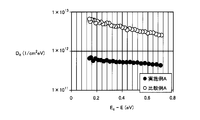
- the interface state density at 0.1 eV below the conduction band is preferably smaller than 1 ⁇ 10 12 cm ⁇ 2 eV ⁇ 1 . Thereby, carrier mobility can be increased more reliably.
- the semiconductor layer may be made of 4H type silicon carbide.
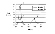
- the ratio of the intensity of the peak appearing near the wavelength of 500 nm to the intensity of the peak appearing near the wavelength of 390 nm is preferably 0.1 or less.
- the on-resistance of the semiconductor device is reduced by reducing the peak appearing in the vicinity of a wavelength of 500 nm in the photoluminescence measurement at room temperature. It was also found that the interface state density can be reduced. More specifically, the peak near the wavelength of 500 nm appears due to the presence of a predetermined stacking fault. The stacking fault corresponding to this peak increases the on-resistance of the semiconductor device, and MOS (Metal- It has been found that the interface state density of the Oxide-Semiconductor structure is increased.
- the peak appearing near the wavelength of 390 nm corresponds to the interband emission of 4H—SiC.
- the peak intensity ratio is 0.1 or less, the on-resistance and interface state density of the semiconductor device can be reduced.
- the ratio of the peak intensities is 0.01 or less, the on-resistance and interface state density of the semiconductor device can be further reduced.
- the state where the peak intensity ratio is 0.1 or less, or 0.01 or less includes the case where the peak intensity ratio is 0. That is, the peak near the wavelength of 500 nm does not have to appear, and most preferably does not appear.
- the method for manufacturing a semiconductor device has a main surface with an off angle of not less than ⁇ 3 ° and not more than + 5 ° with respect to the (0-33-8) plane in the ⁇ 01-10> direction, A step of preparing a substrate made of silicon carbide, a step of forming a semiconductor layer by epitaxial growth on the main surface of the substrate, a step of forming an insulating film in contact with the surface of the semiconductor layer, and the semiconductor layer and the insulating film And a step of adjusting the nitrogen atom concentration so that the maximum value of the nitrogen atom concentration in the region within 10 nm from the interface is 1 ⁇ 10 21 cm ⁇ 3 or more.
- the method for manufacturing a semiconductor device has a main surface with an off angle with respect to the (0-33-8) plane in the ⁇ 01-10> direction of ⁇ 3 ° to + 5 °.
- a step of preparing a substrate made of silicon carbide, a step of forming a semiconductor layer by epitaxial growth on the main surface of the substrate, a step of forming an insulating film in contact with the surface of the semiconductor layer, and the semiconductor layer and the insulating film And a step of adjusting the hydrogen atom concentration so that the maximum value of the hydrogen atom concentration in a region within 10 nm from the interface is 1 ⁇ 10 21 cm ⁇ 3 or more.
- a method for manufacturing a semiconductor device provides a main surface having an off angle of not less than ⁇ 3 ° and not more than + 5 ° with respect to the (0-33-8) plane in the ⁇ 01-10> direction. And a step of preparing a substrate made of silicon carbide, a step of forming a semiconductor layer by epitaxial growth on the main surface of the substrate, a step of forming an insulating film in contact with the surface of the semiconductor layer, and a semiconductor layer, Adjusting the total concentration so that the maximum value of the total concentration of nitrogen atoms and hydrogen atoms in a region within 10 nm from the interface with the insulating film is 1 ⁇ 10 21 cm ⁇ 3 or more.
- the method for manufacturing a semiconductor device may further include a step of containing hydrogen atoms in the region within 10 nm from the interface between the semiconductor layer and the insulating film.
- a step of containing hydrogen atoms in the region within 10 nm from the interface between the semiconductor layer and the insulating film may further include a step of containing hydrogen atoms in the region within 10 nm from the interface between the semiconductor layer and the insulating film.
- the step of containing hydrogen atoms includes the step of heat-treating the substrate on which the insulating film is formed using a gas containing hydrogen atoms as an atmospheric gas. Also good.
- the step of adjusting the nitrogen atom concentration includes a step of heat-treating the substrate on which the insulating film is formed using a gas containing nitrogen atoms as an atmospheric gas. May be included.
- the step of adjusting the nitrogen atom concentration is performed using the inert gas as the atmospheric gas after the step of performing heat treatment using a gas containing nitrogen atoms as the atmospheric gas.
- a step of heat-treating the substrate may be included.
- the method for manufacturing a semiconductor device may further include a step of incorporating nitrogen atoms into the region within 10 nm from the interface between the semiconductor layer and the insulating film.
- a step of incorporating nitrogen atoms into the region within 10 nm from the interface between the semiconductor layer and the insulating film may further include a step of incorporating nitrogen atoms into the region within 10 nm from the interface between the semiconductor layer and the insulating film.
- the step of containing the nitrogen atom includes a step of heat-treating the substrate on which the insulating film is formed using a gas containing a nitrogen atom as an atmospheric gas. May be.
- the step of adjusting the hydrogen atom concentration includes a step of heat-treating the substrate on which the insulating film is formed using a gas containing hydrogen atoms as an atmospheric gas. May be included.
- the step of adjusting the hydrogen atom concentration includes the step of performing a heat treatment using a gas containing hydrogen atoms as the atmospheric gas, and then using the inert gas as the atmospheric gas.
- a step of heat-treating the substrate may be included.
- the gas containing hydrogen atoms may be water vapor or water vapor-containing oxygen.
- hydrogen atoms can be easily introduced in the vicinity of the interface between the semiconductor layer and the insulating film.
- the step of preparing the substrate includes a step of collecting the substrate from a raw crystal made of 4H-type silicon carbide, and another main side opposite to the main surface of the collected substrate. And a step of removing the processing damage layer formed in the region including the surface.
- the on-resistance and interface state density of the semiconductor device are reduced by reducing the peak intensity near the wavelength of 500 nm in the photoluminescence measurement at room temperature. It was found that can be reduced.
- the peak intensity is increased by the following mechanism. Thus, it was found that the on-resistance of the semiconductor device was increased.
- a processing damage layer is formed near the main surface of the substrate.
- the main surface on which the semiconductor layer is formed by epitaxial growth is planarized with high accuracy by polishing or the like.
- the processing damage layer on the semiconductor layer side main surface is removed.
- the processing damage layer near the main surface (back side main surface) opposite to the side on which the semiconductor layer is formed remains.
- a semiconductor layer, an insulating film (oxide film) and the like are formed on the semiconductor-side main surface, and a semiconductor device is manufactured.
- a step of heating to a temperature range of about 1000 ° C. to 1200 ° C. such as thermal oxidation treatment, and a step of passing through the temperature range and heating to a higher temperature range are performed.
- the impurity concentration (for example, nitrogen concentration) in the substrate is high for the purpose of reducing the resistivity of the substrate, a stacking fault is generated from the processing damage layer remaining in the vicinity of the main surface on the back side, and grows inside the substrate. To do.
- the stacking fault grows in the ⁇ 11-20> direction. Therefore, for example, when a general main surface close to the ⁇ 0001 ⁇ plane is adopted as the main surface of the substrate, the stacking fault grown from the processing damage layer grows along the back side main surface, so the semiconductor layer side main surface Will not reach. Therefore, the stacking fault does not propagate to the semiconductor layer formed on the semiconductor layer side main surface. However, when the semiconductor layer side main surface is close to the (0-33-8) plane as in the substrate included in the semiconductor device of the present invention, stacking faults growing from the processing damage layer grow away from the back side main surface. Therefore, it reaches the semiconductor layer side main surface.
- the stacking fault propagates to the semiconductor layer formed on the semiconductor layer side main surface, the peak intensity near the wavelength of 500 nm in the photoluminescence measurement increases, and the on-resistance and interface state density of the semiconductor device increase. To rise.
- the step of preparing the substrate as described above includes the step of removing the processing damage layer, so that the propagation of stacking faults to the semiconductor layer is suppressed, and the on-resistance and interface state density of the semiconductor device are reduced. Can be reduced.
- the substrate in the step of collecting the substrate, the substrate is collected by slicing the raw material crystal, and in the step of removing the processing damage layer, the processing damage formed on the substrate by slicing the raw material crystal. The layer is removed.
- the substrate can be easily collected by slicing the raw crystal. Then, by removing the processing damage layer formed on the substrate by slicing, propagation of stacking faults to the semiconductor layer is suppressed, and the on-resistance and interface state density of the semiconductor device can be reduced.
- the processing damage layer in the step of removing the processing damage layer, may be removed by molten KOH etching.
- the processing damage layer may be removed by dry etching in the step of removing the processing damage layer.
- the processing damage layer in the step of removing the processing damage layer, may be removed by thermal etching.
- the processing damage layer in the step of removing the processing damage layer, may be removed by polishing.
- the processing damage layer can be easily removed by molten KOH etching, dry etching, thermal etching, polishing, or the like.
- the semiconductor device and the manufacturing method thereof of the present invention it is possible to provide a semiconductor device having excellent electrical characteristics such as channel mobility and a manufacturing method thereof.
- FIG. 2 is a flowchart for explaining a method of manufacturing the semiconductor device shown in FIG. It is a cross-sectional schematic diagram for demonstrating each process of the manufacturing method shown in FIG. It is a cross-sectional schematic diagram for demonstrating each process of the manufacturing method shown in FIG. It is a cross-sectional schematic diagram for demonstrating each process of the manufacturing method shown in FIG. It is a cross-sectional schematic diagram for demonstrating each process of the manufacturing method shown in FIG. It is a cross-sectional schematic diagram for demonstrating each process of the manufacturing method shown in FIG. It is a cross-sectional schematic diagram for demonstrating each process of the manufacturing method shown in FIG.
- FIG. 6 is a schematic cross-sectional view illustrating a structure of a semiconductor device in a second embodiment.
- FIG. 9 is a schematic cross-sectional view for illustrating the method for manufacturing the semiconductor device shown in FIG. 8.
- FIG. 9 is a schematic cross-sectional view for illustrating the method for manufacturing the semiconductor device shown in FIG. 8.
- FIG. 9 is a schematic cross-sectional view for illustrating the method for manufacturing the semiconductor device shown in FIG. 8.
- FIG. 9 is a schematic cross-sectional view for illustrating the method for manufacturing the semiconductor device shown in FIG. 8.
- FIG. 6 is a schematic cross-sectional view illustrating a structure of a semiconductor device in a third embodiment.
- 14 is a flowchart for explaining a manufacturing method of the semiconductor device shown in FIG. 13;
- FIG. 10 is a schematic cross-sectional view illustrating the structure of a semiconductor device in a fourth embodiment.
- FIG. 16 is a flowchart for explaining a manufacturing method of the semiconductor device shown in FIG. 15; 17 is a flowchart showing a modification of the method for manufacturing the semiconductor device shown in FIG. 18 is a flowchart showing a second modification of the method for manufacturing the semiconductor device shown in FIG.
- FIG. 6 is a schematic cross sectional view showing a structure of a silicon carbide substrate in a fifth embodiment. It is a flowchart which shows the outline of the manufacturing method of a silicon carbide substrate. 17 is a flowchart showing an outline of a method for manufacturing a silicon carbide substrate in a sixth embodiment.
- FIG. 12 is a schematic cross sectional view for illustrating the method for manufacturing the silicon carbide substrate in the sixth embodiment.
- FIG. 12 is a schematic cross sectional view for illustrating the method for manufacturing the silicon carbide substrate in the sixth embodiment.
- FIG. 12 is a schematic cross sectional view for illustrating the method for manufacturing the silicon carbide substrate in the sixth embodiment.
- FIG. 13 is a schematic cross sectional view showing a structure of a silicon carbide substrate in a seventh embodiment.
- FIG. 22 is a schematic cross sectional view showing a structure of a silicon carbide substrate in an eighth embodiment.
- 20 is a flowchart showing an outline of a method for manufacturing a silicon carbide substrate in an eighth embodiment.
- FIG. 22 is a schematic cross sectional view showing a structure of a silicon carbide substrate in a ninth embodiment.
- 20 is a flowchart showing an outline of a method for manufacturing a silicon carbide substrate in a ninth embodiment.
- FIG. 22 is a schematic cross sectional view showing a structure of a silicon carbide substrate in a tenth embodiment.
- 20 is a flowchart showing an outline of a method for manufacturing a silicon carbide substrate in a tenth embodiment.
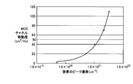
- FIG. 22 is a schematic cross sectional view for illustrating the method for manufacturing the silicon carbide substrate in the tenth embodiment. It is a graph which shows the relationship between the peak value of nitrogen atom concentration, and channel mobility. It is a graph which shows the relationship between the peak value of the total concentration of a nitrogen atom and a hydrogen atom, and channel mobility.
- 10 is a schematic cross-sectional view showing a semiconductor device prepared for measurement in Example 5.
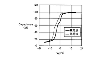
- FIG. It is a graph which shows the CV characteristic about the sample of Example A.
- 6 is a graph showing CV characteristics of a sample of Comparative Example A.
- 10 is a graph showing CV characteristics of the sample of Reference Example A. It is a graph which shows the relationship between the energy at the time of making a conduction band into a reference
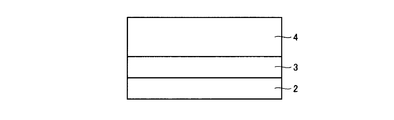
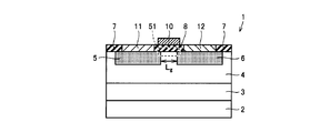
- a semiconductor device 1 shown in FIG. 1 is a lateral MOSFET (Metal-Oxide-Semiconductor Field Effect Transistor) as a semiconductor device, and is formed on a substrate 2 made of 4H-type silicon carbide (SiC).
- MOSFET Metal-Oxide-Semiconductor Field Effect Transistor
- Epitaxial layer 3 made of silicon carbide, p-type layer 4 made of silicon carbide formed on epitaxial layer 3, and an n + region formed at a distance from the region including the surface of p-type layer 4 5, 6 and an oxide film 8 as a gate insulating film located on the channel region between the n + regions 5 and 6, a gate electrode 10 formed on the oxide film 8, an n + region 5, Source electrode 11 and drain electrode 12 formed on each of 6.
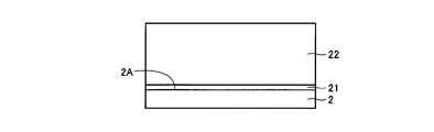
- the substrate 2 is a substrate in which the (0-33-8) plane having an off angle of about 53 ° with respect to the plane orientation ⁇ 0001 ⁇ is the main surface 2A on the epitaxial layer 3 side as a semiconductor layer.
- Substrate 2 contains n-type impurities (impurities that make the conductivity type of substrate 2 n-type; for example, nitrogen).
- Epitaxial layer 3 made of silicon carbide formed on substrate 2 is an undoped layer.
- the p-type layer 4 formed on the epitaxial layer 3 contains a p-type impurity (impurities whose conductivity type of the p-type layer 4 is p-type; for example, aluminum).
- n-type impurities are implanted into the n + regions 5 and 6.
- Oxide films 7 and 8 are formed so as to cover p-type layer 4 and n + regions 5 and 6. Openings are formed in the oxide films 7 and 8 in regions located on the n + regions 5 and 6. Inside the opening, a source electrode 11 and a drain electrode 12 electrically connected to each of the n + regions 5 and 6 are formed.
- a gate electrode 10 is disposed on the oxide film 8 that acts as a gate insulating film.
- the channel length L g which is the distance between the n + regions 5 and 6 can be set to about 100 ⁇ m, for example.
- the channel width may be, for example, about 2 times the channel length L g (about 200 [mu] m).
- the maximum value of the nitrogen atom concentration in the region within 10 nm from the interface between the p-type layer 4 as the semiconductor layer and the oxide film 8 is 1 ⁇ 10 21 cm ⁇ 3 or more.
- the mobility (channel mobility) in the channel region having the channel length L g (the region between the n + regions 5 and 6 in the p-type layer 4) can be made sufficiently large.
- the main surface 2A on the epitaxial layer 3 side of the substrate 2 is a (0-33-8) plane. Therefore, the main surface opposite to the substrate 2 of the p-type layer 4 formed by epitaxial growth and impurity implantation on the main surface 2A is a (0-33-8) plane. As a result, carrier mobility (channel mobility) in the channel region (region including the interface with the oxide film 8 in the n + regions 5 and 6 formed in the p-type layer 4) can be further increased.
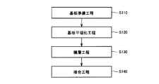
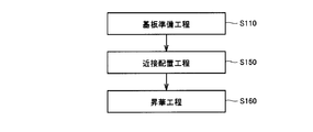
- a silicon carbide substrate preparation step (S10) is performed.
- an n-type conductivity type silicon carbide substrate having a plane orientation (0-33-8) plane as main surface 2A is prepared as substrate 2.
- Such a substrate can be obtained by, for example, a method of cutting a substrate from an ingot (raw material crystal) having a (0001) plane as a main surface so that the (0-33-8) plane is exposed as the main surface 2A. .
- an epitaxial layer forming step (S20) is performed. Specifically, as shown in FIG. 3, undoped silicon carbide epitaxial layer 3 is formed on substrate 2 by epitaxial growth.
- an injection step (S30) is performed. Specifically, first, p-type impurities (for example, aluminum (Al)) are implanted into the epitaxial layer 3 to form the p-type layer 4 as shown in FIG. Next, n + regions 5 and 6 are formed by implanting n-type impurities as shown in FIG. As this n-type impurity, for example, phosphorus (P) can be used. In forming the n + regions 5 and 6, any known method can be used.
- p-type impurities for example, aluminum (Al)
- Al aluminum
- n + regions 5 and 6 are formed by implanting n-type impurities as shown in FIG.
- n-type impurity for example, phosphorus (P) can be used.
- P phosphorus
- an activation annealing process is performed to activate the implanted impurities.
- this activation annealing treatment for example, conditions where the heating temperature is 1700 ° C. and the heating time is 30 minutes may be used.
- a gate insulating film forming step (S40) is performed. Specifically, by oxidizing the upper surfaces of the p-type layer 4 and the n + regions 5 and 6, an oxide film 7 as a gate insulating film is formed as shown in FIG. As the thickness of the oxide film 7, for example, a value of 40 nm can be used.
- a nitrogen annealing step (S50) is performed as shown in FIG. Specifically, heat treatment is performed using nitrogen monoxide (NO) gas as the atmospheric gas.
- NO nitrogen monoxide
- conditions for this heat treatment for example, a condition in which the heating temperature is 1100 ° C. and the heating time is 1 hour can be used.
- nitrogen atoms can be introduced into the interface region between oxide film 7 and p-type layer 4 and n + regions 5 and 6.
- an annealing process using an inert gas for example, an annealing process using argon (Ar) gas as the atmospheric gas is performed. May be.
- an electrode formation step (S60) is performed as shown in FIG. Specifically, a resist film having a pattern is formed on the oxide film 7 by photolithography. Using this resist film as a mask, the oxide film 7 is partially removed to form an opening 15 in a region located above the n + regions 5 and 6. Inside the opening 15, a conductor film to be the source electrode 11 and the drain electrode 12 is formed as shown in FIG. This conductor film is formed with the above-described resist film remaining. Thereafter, the resist film is removed, and the conductive film located on the oxide film 7 is removed (lifted off) together with the resist film, whereby the source electrode 11 and the drain electrode 12 can be formed as shown in FIG. it can. At this time, the oxide film 8 (a part of the oxide film 7 shown in FIG. 6) located between the source electrode 11 and the drain electrode 12 becomes a gate insulating film of the semiconductor device.
- a gate electrode 10 (see FIG. 1) is further formed on the oxide film 8 acting as a gate insulating film.
- the following method can be used. For example, a resist film having an opening pattern located in a region on the oxide film 8 is formed in advance, and a conductor film constituting the gate electrode is formed so as to cover the entire surface of the resist film. Then, by removing the resist film, the conductor film other than the portion of the conductor film to be the gate electrode is removed (lifted off). As a result, the gate electrode 10 is formed as shown in FIG. In this way, the semiconductor device 1 as shown in FIG. 1 can be obtained.
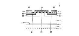
- the semiconductor device 1 is a vertical DiMOSFET (Double Implanted MOSFET), and includes a substrate 2, a buffer layer 21, a breakdown voltage holding layer 22, a p region 23, an n + region 24, a p + region 25, and an oxide film. 26, the source electrode 11 and the upper source electrode 27, the gate electrode 10, and the drain electrode 12 formed on the back surface side of the substrate 2.
- buffer layer 21 made of silicon carbide is formed on main surface 2A of substrate 2 made of silicon carbide of n-type conductivity.
- Buffer layer 21 is n-type in conductivity type and has a thickness of 0.5 ⁇ m, for example.
- the concentration of the n-type impurity in the buffer layer 21 can be set to 5 ⁇ 10 17 cm ⁇ 3 , for example.
- a breakdown voltage holding layer 22 is formed on the buffer layer 21.
- the breakdown voltage holding layer 22 is made of silicon carbide of n-type conductivity, and has a thickness of 10 ⁇ m, for example. Further, as the concentration of the n-type impurity in the breakdown voltage holding layer 22, for example, a value of 5 ⁇ 10 15 cm ⁇ 3 can be used.
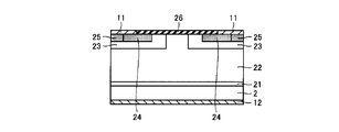
- p regions 23 having a p-type conductivity are formed at intervals.
- n + region 24 is formed in a region including the main surface of p region 23.
- a p + region 25 is formed at a position adjacent to the n + region 24.
- An oxide film 26 is formed so as to extend up to.
- a gate electrode 10 is formed on the oxide film 26.
- the source electrode 11 is formed so as to be in contact with the n + region 24 and the p + region 25.
- An upper source electrode 27 is formed on the source electrode 11.
- the drain electrode 12 is formed on the main surface (back surface) opposite to the main surface on which the buffer layer 21 is formed.
- the maximum value of the nitrogen atom concentration in a region within 10 nm from the interface between the oxide film 26 and the n + region 24, p + region 25, p region 23, and breakdown voltage holding layer 22 as a semiconductor layer is 1 ⁇ 10 It is 21 cm ⁇ 3 or more.
- the mobility of the channel region under the oxide film 26 (part of the p region 23 that is in contact with the oxide film 26 and between the n + region 24 and the breakdown voltage holding layer 22) is shown in FIG. Improvements can be made in the same manner as in the case of the semiconductor device 1.
- the main surface 2A on the buffer layer 21 side of the substrate 2 is a (0-33-8) plane. Therefore, the main surface opposite to the substrate 2 of the p region 23 formed by epitaxial growth and impurity implantation on the main surface 2A is a (0-33-8) plane. As a result, carrier mobility (channel mobility) in the channel region can be further increased.
- a method for manufacturing the semiconductor device 1 shown in FIG. 8 will be described with reference to FIGS.
- a silicon carbide substrate preparation step S10 is performed.
- substrate 2 (see FIG. 9) made of silicon carbide having (0-33-8) plane as the main surface is prepared in the same manner as in the method of manufacturing the semiconductor device in the first embodiment.
- the substrate 2 for example, a substrate having an n-type conductivity and a substrate resistance of 0.02 ⁇ cm may be used as the substrate 2 (see FIG. 9).
- buffer layer 21 is formed on main surface 2 ⁇ / b> A of substrate 2.
- an epitaxial layer made of silicon carbide of n-type conductivity for example, having a thickness of 0.5 ⁇ m is formed.
- a value of 5 ⁇ 10 17 cm ⁇ 3 can be used as the impurity concentration in the buffer layer 21.
- a breakdown voltage holding layer 22 is formed on the buffer layer 21 as shown in FIG.
- a layer made of silicon carbide of n-type conductivity is formed by an epitaxial growth method.
- a value of 10 ⁇ m can be used as the thickness of the breakdown voltage holding layer 22.
- concentration of the n-type conductive impurity in the breakdown voltage holding layer 22 for example, a value of 5 ⁇ 10 15 cm ⁇ 3 can be used.
- an implantation step (S30) is performed in the same manner as the step shown in FIG. Specifically, by using an oxide film formed by photolithography and etching as a mask, an impurity having a conductivity type of p-type is implanted into the breakdown voltage holding layer 22, thereby forming the p region 23 as shown in FIG. Form. Further, after removing the used oxide film, an oxide film having a new pattern is formed again by photolithography and etching. Then, using the oxide film as a mask, an n-type impurity is implanted into a predetermined region, thereby forming an n + region 24. Further, the p + region 25 is formed by implanting an impurity having a p-type conductivity by a similar method. As a result, a structure as shown in FIG. 10 is obtained.
- activation annealing is performed.
- this activation annealing treatment for example, argon gas is used as an atmospheric gas, and conditions such as a heating temperature of 1700 ° C. and a heating time of 30 minutes can be used.
- a gate insulating film forming step (S40) is performed as in the step shown in FIG. Specifically, as illustrated in FIG. 11, an oxide film 26 is formed so as to cover the breakdown voltage holding layer 22, the p region 23, the n + region 24, and the p + region 25.
- the oxide film 26 may be formed by dry oxidation (thermal oxidation), for example.
- dry oxidation thermal oxidation
- conditions for this dry oxidation conditions such as a heating temperature of 1200 ° C. and a heating time of 30 minutes can be used.
- a nitrogen annealing step (S50) is performed as in the step shown in FIG. Specifically, the annealing process is performed using nitrogen monoxide (NO) as the atmosphere gas.
- NO nitrogen monoxide
- the heating temperature is 1100 ° C. and the heating time is 120 minutes.
- nitrogen atoms are introduced near the interface between the oxide film 26 and the underlying breakdown voltage holding layer 22, p region 23, n + region 24, and p + region 25.
- annealing using nitrogen monoxide as an atmospheric gas annealing using nitrogen monoxide as an atmospheric gas.
- argon (Ar) gas which is an inert gas may be performed.
- argon gas may be used as the atmosphere gas
- the heating temperature may be 1100 ° C. and the heating time may be 60 minutes.
- an electrode formation step (S60) is performed in the same manner as the step shown in FIG. Specifically, a resist film having a pattern is formed on the oxide film 26 by using a photolithography method. Then, using the resist film as a mask, portions of the oxide film located on the n + region 24 and the p + region 25 are removed by etching. Thereafter, on the resist film, in the opening formed in the oxide film 26, the region in contact with the n + region 24 and the p + region 25, and the main surface opposite to the buffer layer 21 of the substrate 2, A conductor film such as metal is formed. Thereafter, by removing the resist film, the conductor film located on the resist film is removed (lifted off).
- nickel (Ni) can be used as the conductor.
- the source electrode 11 and the drain electrode 12 can be obtained as shown in FIG.
- Ar argon
- a semiconductor device 1 according to the present invention basically has the same configuration as that of the semiconductor device 1 shown in FIG. 1, but an interface between a p-type layer 4 as a semiconductor layer and an oxide film 8. 1 differs from the semiconductor device 1 shown in FIG. 1 in that the maximum value of the hydrogen atom concentration is 1 ⁇ 10 21 cm ⁇ 3 or more in the boundary region 41 including the region within 10 nm from the region. Even in this case, similarly to the semiconductor device shown in FIG. 1, the mobility (channel mobility) in the channel region including the boundary region 41 can be set to a sufficiently large value. In the semiconductor device 1 shown in FIG.
- the hydrogen atoms contained in the boundary region 41 are in a region within 10 nm from the interface between the p-type layer 4 and the oxide film 8 of the semiconductor device 1 shown in FIG. 1. This is presumably because the interface state is reduced similarly to the nitrogen atom contained.
- the manufacturing method of the semiconductor device shown in FIG. 14 is basically the same as the manufacturing method of the semiconductor device shown in FIG. 2, but a hydrogen annealing step (S70) is performed instead of the nitrogen annealing step (S50) in FIG. Different points are implemented. Specifically, the silicon carbide substrate preparation step (S10), the epitaxial layer formation step (S20), the implantation step (S30), and the gate insulating film formation step (S40) are performed in the same manner as the manufacturing method shown in FIG. . Thereafter, a hydrogen annealing step (S70) is performed. Specifically, heat treatment is performed using hydrogen gas (H 2 ) gas as the atmosphere gas.
- H 2 hydrogen gas
- a condition in which the heating temperature is 1100 ° C. and the heating time is 1 hour can be used.
- hydrogen atoms can be introduced into the interface region between oxide film 7 and p-type layer 4 and n + regions 5 and 6.
- an annealing process using an inert gas for example, an annealing process using argon (Ar) gas as the atmosphere gas is performed. May be.
- water vapor or water vapor-containing oxygen gas may be used as the atmospheric gas instead of hydrogen gas.
- the semiconductor device 1 shown in FIG. 13 can be obtained by performing the electrode forming step (S60) in the same manner as the manufacturing method shown in FIG.
- semiconductor device 1 in the present embodiment basically has the same configuration as that of semiconductor device 1 shown in FIG. 1, but includes p-type layer 4 as a semiconductor layer, oxide film 8, and the like.
- the maximum value of the total concentration of nitrogen atoms and hydrogen atoms is 1 ⁇ 10 21 cm ⁇ 3 or more in the boundary region 51 including the region within 10 nm from the interface of Yes.
- the mobility (channel mobility) in the channel region including the boundary region 41 can be set to a sufficiently large value.
- the manufacturing method of the semiconductor device shown in FIG. 16 is basically the same as the manufacturing method of the semiconductor device shown in FIG. 2, but after the nitrogen annealing step (S50) in FIG.
- the hydrogen annealing step (S70) is performed before ().
- a silicon carbide substrate preparation step (S10), an epitaxial layer formation step (S20), an implantation step (S30), a gate insulating film formation step (S40), nitrogen annealing Step (S50) is performed.
- a hydrogen annealing step (S70) is performed.
- this step (S70) the same conditions (annealing conditions using hydrogen gas) as in the hydrogen annealing step (S70) in the manufacturing method of Embodiment 3 can be used.
- nitrogen atoms and hydrogen atoms can be introduced into the interface region between oxide film 7 and p-type layer 4 and n + regions 5 and 6.
- water vapor or water vapor-containing oxygen gas may be used as the atmospheric gas instead of hydrogen gas.
- the hydrogen annealing step (S70) may be performed prior to the nitrogen annealing step (S50).
- the hydrogen annealing step (S70) and the nitrogen annealing step (S50) may be performed simultaneously by performing a heat treatment using an atmosphere gas containing hydrogen atoms and nitrogen atoms.
- the semiconductor device 1 shown in FIG. 15 can be obtained by performing the electrode forming step (S60) in the same manner as the manufacturing method shown in FIG.
- the manufacturing method of the semiconductor device shown in FIG. 17 is basically the same as the manufacturing method of the semiconductor device shown in FIG. 16, but after the hydrogen annealing step (S70) in FIG. ) Is different in that a post heat treatment step (S80) is performed.
- a silicon carbide substrate preparation step (S10), an epitaxial layer formation step (S20), an implantation step (S30), a gate insulating film formation step (S40), nitrogen annealing A process (S50) and a hydrogen annealing process (S70) are performed. Thereafter, a post heat treatment step (S80) is performed.
- an annealing process using an inert gas is performed.
- an inert gas for example, argon (Ar)
- the heating temperature is 1100 ° C.
- the heating time is 60 minutes.
- the semiconductor device 1 shown in FIG. 15 can be obtained by performing the electrode forming step (S60) in the same manner as the manufacturing method shown in FIG.
- a heat treatment step similar to the above-described post heat treatment step (S80) may be additionally performed between the nitrogen annealing step (S50) and the hydrogen annealing step (S70).
- the hydrogen annealing step (S70) may be performed prior to the nitrogen annealing step (S50).
- the hydrogen annealing step (S70) and the nitrogen annealing step (S50) may be performed simultaneously by performing a heat treatment using an atmosphere gas containing hydrogen atoms and nitrogen atoms.
- the manufacturing method of the semiconductor device shown in FIG. 18 is basically the same as the manufacturing method of the semiconductor device shown in FIG. 17, but is different from the manufacturing method shown in FIG. 17 in the silicon carbide substrate preparation step.
- the silicon carbide substrate preparation step in the present modification includes a raw material crystal preparation step (S11), a slicing step (S12), and a processing damage layer removal step (S13). It is out.
- a raw material crystal made of 4H type silicon carbide is produced, for example, by a sublimation method.
- step (S12) the raw material crystal produced in step (S11) is sliced, and substrate 2 is collected. At this time, the raw material is such that one main surface of the substrate 2 is a (0-33-8) plane (carbon surface side surface) and the other main surface is a (03-38) surface (silicon surface side surface). Crystals are sliced.
- step (S13) at least the (03-38) plane processing damage layer is removed from the processing damage layers formed in the region including the main surfaces on both sides of the substrate 2 by slicing in step (S12).
- This processing damage layer can be removed by, for example, etching treatment such as molten KOH etching, dry etching, thermal etching, or polishing.
- the main surface on the (0-33-8) plane side on which an epitaxial layer is to be formed in a later step is a surface suitable for epitaxial growth by combining mechanical polishing (MP), chemical mechanical polishing (CMP), etc. The surface is flattened to be rough.
- the processing damage layer is also removed from the region including the main surface on the (0-33-8) plane side.
- the region including the main surface on the (0-33-8) plane side may be subjected to the above planarization after the processing damage layer is removed in the same manner as the (03-38) plane side. .
- the epitaxial layer forming step (S20), the implantation step (S30), the gate insulating film forming step (S40), and the nitrogen annealing step By performing the S50), the hydrogen annealing step (S70), the post heat treatment step (S80), and the electrode formation step (S60), the semiconductor device according to the second modification is obtained.
- the processing damage layer introduced into the region including the (03-38) surface of the substrate 2 in the step (S12) is removed in the step (S13). Further, the processing damage layer introduced into the region including the (0-33-8) plane of the substrate 2 is removed in a polishing process such as MP or CMP. Therefore, the growth of stacking faults from the processing damage layer in the process such as the gate insulating film forming step (S40) heated to about 1000 ° C. to 1200 ° C. is suppressed.
- the lateral MOSFET is shown as the semiconductor device 1, but the features of the third and fourth embodiments may be applied to the vertical DiMOSFET shown in FIG. That is, in the semiconductor device 1 shown in FIG. 8, hydrogen atoms in a region within 10 nm from the interface between the oxide film 26 and the n + region 24, the p + region 25, the p region 23, and the breakdown voltage holding layer 22 as semiconductor layers.
- the maximum value of the concentration or the maximum value of the total concentration of nitrogen atoms and hydrogen atoms can be 1 ⁇ 10 21 cm ⁇ 3 or more.
- the main surface 2A on the semiconductor side of the substrate 2 can be a (0-33-8) plane.
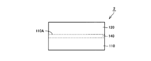
- the semiconductor device according to the present embodiment has basically the same structure as the semiconductor device according to the first to fourth embodiments and has the same effects. However, the semiconductor device according to the present embodiment is different from the first to fourth embodiments in the structure of the substrate 2.
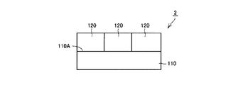
- substrate 2 constituting semiconductor device 1 in the present embodiment includes base layer 110 made of silicon carbide and single crystal silicon carbide, and is arranged on one main surface 110 ⁇ / b> A of base layer 110.
- SiC layer 120 formed.
- Base layer 110 and SiC layer 120 are made of different crystals.
- the defect density of SiC layer 120 is smaller than the defect density of base layer 110.
- High-quality silicon carbide single crystal is difficult to increase in diameter.
- a substrate having a predetermined shape and size is required. Therefore, even when a high-quality silicon carbide single crystal (for example, a silicon carbide single crystal having a low defect density) is obtained, a region that cannot be processed into a predetermined shape by cutting or the like may not be used effectively.
- substrate 2 constituting the semiconductor device of the present embodiment includes base layer 110 made of silicon carbide and SiC layer 120 made of single crystal silicon carbide and disposed on base layer 110.
- the defect density of the SiC layer 120 is smaller than the defect density of the base layer 110. Therefore, the base substrate 110 made of silicon carbide crystal having a high defect density and low quality is processed into the predetermined shape and size to form the base layer 110, and the desired shape of the high quality on the base layer 110 is obtained.
- a silicon carbide single crystal in which the above is not realized can be arranged as SiC layer 120. Since the substrate 2 obtained in this way is unified in a predetermined shape and size, the production of the semiconductor device 1 can be made efficient.
- the silicon carbide substrate obtained in this way can manufacture semiconductor device 1 using high quality SiC layer 120, a silicon carbide single crystal can be used effectively.
- a semiconductor device capable of reducing the manufacturing cost can be provided.
- the half width of the X-ray rocking curve of the SiC layer 120 may be smaller than the half width of the X-ray rocking curve of the base layer 110.
- the impurity concentration of the base layer 110 is higher than 2 ⁇ 10 19 cm ⁇ 3
- the impurity concentration of the SiC layer 120 is higher than 5 ⁇ 10 18 cm ⁇ 3 and lower than 2 ⁇ 10 19 cm ⁇ 3. Also good.
- the impurity concentration is less than 2 ⁇ 10 19 cm ⁇ 3 , generation of stacking faults due to heat treatment (for example, thermal oxidation treatment) in the semiconductor device manufacturing process is suppressed.
- heat treatment for example, thermal oxidation treatment
- it exceeds 2 ⁇ 10 19 cm ⁇ 3 it is difficult to suppress stacking faults. Therefore, when the impurity concentration exceeds 2 ⁇ 10 19 cm ⁇ 3 , it is preferable to perform the step of removing the processing damage layer as in the second modification of the fourth embodiment.
- impurity concentration in the substrate 2 made of silicon carbide is 2 ⁇ 10 19 cm -3, with small layer provided (base layer 110) resistivity, impurity concentration is smaller than 2 ⁇ 10 19 cm -3
- the layer (SiC layer 120) By disposing the layer (SiC layer 120) on the base layer 110, even if heat treatment in the device manufacturing process is subsequently performed, at least the SiC layer 120 causes stacking faults and the processing damage layer is removed. It can suppress without doing.
- the semiconductor device 1 by forming an epitaxially grown layer (active layer) made of SiC on the SiC layer 120 to produce the semiconductor device 1, while reducing the resistivity of the silicon carbide substrate 2 due to the presence of the base layer 110, It is possible to suppress the influence of stacking faults that may occur in the base layer 110 from affecting the characteristics of the semiconductor device.
- the impurity concentration of the SiC layer 120 is 5 ⁇ 10 18 cm ⁇ 3 or less, the resistivity of the SiC layer 120 becomes too high, so that the vertical semiconductor device (in the thickness direction of the substrate 2) as shown in FIG. There may be a problem that the substrate 2 suitable for a semiconductor device through which a current flows cannot be obtained.
- the impurity concentration of the base layer 110 is higher than 2 ⁇ 10 19 cm ⁇ 3
- the impurity concentration of the SiC layer 120 is higher than 5 ⁇ 10 18 cm ⁇ 3 and lower than 2 ⁇ 10 19 cm ⁇ 3.
- the micropipe density of the SiC layer 120 is smaller than the micropipe density of the base layer 110.
- the threading screw dislocation density of SiC layer 120 is preferably smaller than the threading screw dislocation density of base layer 110.
- the threading edge dislocation density of SiC layer 120 is preferably smaller than the threading edge dislocation density of base layer 110.
- the basal plane dislocation density of SiC layer 120 is preferably smaller than the basal plane dislocation density of base layer 110.
- the mixed dislocation density of SiC layer 120 is preferably smaller than the mixed dislocation density of base layer 110.
- the stacking fault density of SiC layer 120 is preferably smaller than the stacking fault density of base layer 110.
- the point defect density of SiC layer 120 is preferably smaller than the point defect density of base layer 110.
- the SiC layer in which the defect density such as the micropipe density, the threading screw dislocation density, the threading edge dislocation density, the basal plane dislocation density, the mixed dislocation density, the stacking fault density, and the point defect density is reduced as compared with the base layer 110.
- a high-quality active layer epitaxial growth layer
- the base layer 110 and the SiC layer 120 are bonded, for example. Thereby, silicon carbide substrate 2 on which SiC layer 120 is arranged can be easily obtained while suppressing the propagation of defects in base layer 110. At this time, the base layer 110 and the SiC layer 120 may be joined directly, or may be joined via an intermediate layer.
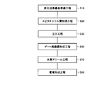
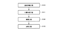
- a substrate preparation step is first performed as a step (S110).
- step (S110) referring to FIG. 19, for example, base substrate 110 made of single crystal silicon carbide and SiC substrate 120 made of single crystal silicon carbide are prepared.
- main surface 120A of SiC substrate 120 is the main surface of substrate 2 obtained by this manufacturing method, so the plane orientation of main surface 120A of SiC substrate 120 is selected in accordance with the plane orientation of the desired main surface.
- SiC substrate 120 whose main surface is a (0-33-8) plane is prepared.
- the base substrate 110 for example, a substrate having an impurity concentration higher than 2 ⁇ 10 19 cm ⁇ 3 is employed.
- SiC substrate 120 for example, a substrate having an impurity concentration larger than 5 ⁇ 10 18 cm ⁇ 3 and smaller than 2 ⁇ 10 19 cm ⁇ 3 is employed.
- a substrate flattening step is performed as a step (S120).
- This step (S120) is not an essential step, but can be performed when the flatness of the base substrate 110 and the SiC substrate 120 prepared in the step (S110) is insufficient. Specifically, for example, the main surface of base substrate 110 or SiC substrate 120 is polished. On the other hand, the manufacturing cost can be reduced by omitting this step.
- an etching process may be performed to remove a processing damage layer formed in a region including the main surface when the SiC substrate 120 is collected from the raw crystal (ingot). The etching process can be performed by, for example, molten KOH etching.
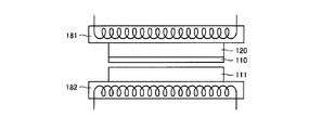
- a stacking step is performed.
- base substrate 110 and SiC substrate 120 are stacked so that their main surfaces 110A and 120B are in contact with each other, and a laminated substrate is manufactured.
- a joining step is performed as a step (S140).
- step (S140) base substrate 110 and SiC substrate 120 are joined by heating the laminated substrate to a temperature range equal to or higher than the sublimation temperature of silicon carbide, for example.
- substrate 2 including base layer 110 and SiC layer 120 is completed.
- this substrate 2 is used, and the semiconductor device 1 is manufactured in the same manner as in the first to fourth embodiments.
- the heating temperature of the multilayer substrate in the step (S140) is preferably 1800 ° C. or higher and 2500 ° C. or lower.
- the heating temperature is lower than 1800 ° C., it takes a long time to join base substrate 110 and SiC substrate 120, and the manufacturing efficiency of substrate 2 decreases.
- the heating temperature exceeds 2500 ° C., the surfaces of the base substrate 110 and the SiC substrate 120 are roughened, and there is a possibility that the generation of defects in the manufactured substrate 2 increases.
- the heating temperature of the laminated substrate in the step (S140) is preferably 1900 ° C. or higher and 2100 ° C. or lower.
- the pressure of the atmosphere in the heating in the step (S140) is 10 ⁇ 5 Pa to 10 6 Pa, more preferably 10 ⁇ 2 Pa to 10 4 Pa, so that the above bonding is performed with a simple apparatus. can do.
- the atmosphere at the time of a heating in a process (S140) is an inert gas atmosphere.
- the atmosphere is more preferably an inert gas atmosphere containing at least one selected from the group consisting of argon, helium and nitrogen.
- FIGS. 6 Next, as a sixth embodiment, another method for manufacturing a substrate constituting the semiconductor device of the present invention will be described with reference to FIGS.
- the substrate manufacturing method according to the sixth embodiment is basically performed in the same manner as in the fifth embodiment. However, the substrate manufacturing method in the sixth embodiment is different from that in the fifth embodiment in the formation process of the base layer 110.
- a substrate preparation step is first performed as a step (S110).
- SiC substrate 120 is prepared in the same manner as in the fifth embodiment, and source substrate 111 made of silicon carbide is prepared.
- Raw material substrate 111 may be made of single crystal silicon carbide, may be made of polycrystalline silicon carbide, or may be a sintered body of silicon carbide. Further, a raw material powder made of silicon carbide can be employed instead of the raw material substrate 111.
- a proximity placement step is performed as a step (S150).
- SiC substrate 120 and raw material substrate 111 are held by first heater 181 and second heater 182 arranged to face each other.
- SiC substrate 120 and raw material substrate 111 are arranged close to each other so that main surface 120B and main surface 111A as the main surfaces face each other at an interval of 1 ⁇ m or more and 1 cm or less, for example, an interval of about 1 mm. Is done.
- a sublimation step is performed as a step (S160).
- SiC substrate 120 is heated to a predetermined substrate temperature by first heater 181.
- the raw material substrate 111 is heated to a predetermined raw material temperature by the second heater 182.
- SiC is sublimated from the surface of the source substrate by heating source substrate 111 to the source temperature.
- the substrate temperature is set lower than the raw material temperature. Specifically, for example, the substrate temperature is set to be 1 ° C. or more and 100 ° C. or less lower than the raw material temperature.
- the substrate temperature is, for example, 1800 ° C. or higher and 2500 ° C. or lower.
- SiC sublimated from the raw material substrate 111 reaches a surface of the SiC substrate 120 and becomes a solid, thereby forming the base layer 110.
- all of the SiC constituting the raw material substrate 111 is sublimated and moves onto the surface of the SiC substrate 120.
- the step (S160) is completed, and the substrate 2 shown in FIG. 19 is completed.
- Embodiment 7 which is still another embodiment of the present invention will be described.
- the semiconductor device according to the seventh embodiment basically has the same structure as that of the fifth embodiment. However, the semiconductor device of the seventh embodiment is different from that of the fifth embodiment in the manufacturing method.
- a substrate having a structure different from that in the fifth embodiment is prepared in the silicon carbide substrate preparation step performed as step (S10).
- a plurality of SiC layers 120 are arranged side by side in plan view. That is, a plurality of SiC layers 120 are arranged along main surface 110 ⁇ / b> A of base layer 110. More specifically, the plurality of SiC layers 120 are arranged in a matrix so that adjacent SiC layers 120 on base layer 110 are in contact with each other.
- substrate 2 in the present embodiment is substrate 2 that can be handled as a large-diameter substrate having high-quality SiC layer 120.
- the manufacturing process of the semiconductor device can be made efficient.
- the substrate 2 in the seventh embodiment is implemented by arranging a plurality of SiC substrates 120 in a plane on the base substrate 110 in the step (S130) in the fifth embodiment (see FIG. 19) or
- the first heater 181 holds the plurality of SiC substrates 120 in a state of being arranged in a plane (see FIG. 22). Can be produced in the same manner.
- the substrate 2 is used and the semiconductor device 1 is manufactured.
- the semiconductor device 1 is manufactured by forming a plurality of semiconductor layers on the SiC layer 120 of the substrate 2 shown in FIG. At this time, each semiconductor device 1 is manufactured so as not to cross the boundary region between adjacent SiC layers 120.
- the semiconductor device 1 according to the eighth embodiment basically has the same structure as the semiconductor device 1 according to the fifth embodiment, and has the same effects. However, the semiconductor device 1 of the eighth embodiment is different from that of the fifth embodiment in the structure of the substrate 2.
- amorphous SiC layer 140 as an intermediate layer made of amorphous SiC is arranged between base layer 110 and SiC layer 120.
- Base layer 110 and SiC layer 120 are connected by amorphous SiC layer 140. Due to the presence of the amorphous SiC layer 140, for example, the substrate 2 in which the base layer 110 and the SiC layer 120 having different impurity concentrations are stacked can be easily manufactured.
- a substrate preparation step is performed as step (S110) in the same manner as in the fifth embodiment, and base substrate 110, SiC substrate 120, Is prepared.
- a Si layer forming step is performed as a step (S111).
- an Si layer having a thickness of, for example, about 100 nm is formed on one main surface of base substrate 110 prepared in step (S110).
- the Si layer can be formed by, for example, a sputtering method.
- step (S130) SiC substrate 120 prepared in step (S110) is placed on the Si layer formed in step (S111). Thereby, a laminated substrate in which the SiC substrate 120 is laminated on the base substrate 110 with the Si layer interposed therebetween is obtained.
- a heating step is performed as a step (S170).
- the laminated substrate produced in the step (S130) is heated to about 1500 ° C. in a mixed gas atmosphere of hydrogen gas and propane gas having a pressure of 1 ⁇ 10 3 Pa, for example, for about 3 hours. Retained.
- carbon is supplied to the Si layer mainly by diffusion from the base substrate 110 and the SiC substrate 120, and an amorphous SiC layer 140 is formed as shown in FIG.
- substrate 2 in the eighth embodiment in which base layer 110 and SiC layer 120 having different impurity concentrations are connected by amorphous SiC layer 140 can be easily manufactured.
- Embodiment 9 which is still another embodiment of the present invention will be described.
- the semiconductor device 1 according to the ninth embodiment basically has the same structure as the semiconductor device 1 according to the fifth embodiment, and has the same effects. However, the semiconductor device 1 of the ninth embodiment is different from that of the fifth embodiment in the structure of the substrate 2.
- substrate 2 in the ninth embodiment ohmic as an intermediate layer formed by siliciding at least a part of a metal layer between base layer 110 and SiC layer 120.
- the contact layer 150 is different from the fifth embodiment in that the contact layer 150 is formed.
- Base layer 110 and SiC layer 120 are connected by ohmic contact layer 150. Due to the presence of the ohmic contact layer 150, for example, the substrate 2 in which the base layer 110 and the SiC layer 120 having different impurity concentrations are stacked can be easily manufactured.
- a substrate preparation step is performed as step (S110) in the same manner as in the fifth embodiment, and base substrate 110, SiC substrate 120, Is prepared.
- a metal film forming step is performed as a step (S112).
- a metal film is formed, for example, by vapor-depositing metal on one main surface of the base substrate 110 prepared in the step (S110).
- This metal film contains, for example, at least one selected from metals that form silicide when heated, for example, nickel, molybdenum, titanium, aluminum, and tungsten.
- step (S130) SiC substrate 120 prepared in step (S110) is placed on the metal film formed in step (S112). Thereby, a laminated substrate is obtained in which SiC substrate 120 is laminated on base substrate 110 with a metal film interposed therebetween.
- a heating step is performed as a step (S170).
- the multilayer substrate manufactured in step (S130) is heated to about 1000 ° C. in an inert gas atmosphere such as argon.
- an inert gas atmosphere such as argon.
- the metal film the region in contact with the base substrate 110 and the region in contact with the SiC substrate
- the ohmic contact layer 150 that makes ohmic contact with the base layer 110 and the SiC layer 120 is formed.
- substrate 2 in the ninth embodiment in which base layer 110 and SiC layer 120 having different impurity concentrations are connected by ohmic contact layer 150 can be easily manufactured.
- Embodiment 10 which is still another embodiment of the present invention will be described.
- the semiconductor device 1 according to the tenth embodiment basically has the same structure as the semiconductor device 1 according to the fifth embodiment, and has the same effects. However, the semiconductor device 1 according to the tenth embodiment is different from the fifth embodiment in the structure of the substrate 2.
- carbon layer 160 as an intermediate layer is formed between base layer 110 and SiC layer 120. It is different from the case. Base layer 110 and SiC layer 120 are connected by carbon layer 160. Due to the presence of the carbon layer 160, for example, the substrate 2 in which the base layer 110 and the SiC layer 120 having different impurity concentrations are stacked can be easily manufactured.
- step (S110) is performed in the same manner as in the fifth embodiment, and then step (S120) is performed in the same manner as in the fifth embodiment as necessary.
- a carbon adhesive is applied onto the main surface of base substrate 110, whereby precursor layer 161 is formed.
- a carbon adhesive what consists of resin, graphite fine particles, and a solvent can be employ
- the resin a resin that becomes non-graphitizable carbon when heated, such as a phenol resin, can be employed.
- the solvent for example, phenol, formaldehyde, ethanol, or the like can be used.
- the coating amount of the carbon adhesive is preferably 10 mg / cm 2 or more and 40 mg / cm 2 or less, and more preferably 20 mg / cm 2 or more and 30 mg / cm 2 or less.
- the thickness of the carbon adhesive to be applied is preferably 100 ⁇ m or less, and more preferably 50 ⁇ m or less.
- a stacking step is performed.
- SiC substrate 120 is placed in contact with precursor layer 161 formed in contact with the main surface of base substrate 110, and the laminated substrate is Produced.
- a pre-baking step is performed.
- the solvent component is removed from the carbon adhesive constituting the precursor layer 161 by heating the laminated substrate.
- the multilayer substrate is gradually heated to a temperature range exceeding the boiling point of the solvent component while applying a load to the multilayer substrate in the thickness direction. This heating is preferably performed while the base substrate 110 and the SiC substrate 120 are pressure-bonded using a clamp or the like. Further, by performing pre-baking (heating) as much as possible, degassing from the adhesive proceeds, and the strength of bonding can be improved.
- a firing step is performed as a step (S190).
- the laminated substrate heated in the step (S180) and pre-baked with the precursor layer 161 is heated to a high temperature, preferably 900 ° C. to 1100 ° C., for example, 1000 ° C., preferably 10 minutes to 10 minutes.
- the precursor layer 161 is fired by being held for a period of time, for example, 1 hour.
- an atmosphere at the time of firing an inert gas atmosphere such as argon is adopted, and the pressure of the atmosphere can be set to atmospheric pressure, for example.
- the precursor layer 161 becomes the carbon layer 160 made of carbon.
- substrate 2 in the tenth embodiment in which base substrate (base layer) 10 and SiC substrate (SiC layer) 20 are bonded by carbon layer 160 is obtained.
- a semiconductor device 1 according to the present invention has a main surface having an off angle of ⁇ 3 ° to + 5 ° with respect to the (0-33-8) plane in the ⁇ 01-10> direction, and is a substrate 2 made of silicon carbide. And a semiconductor layer (p-type layer 4 in FIG. 1 and p region 23 in FIG. 8) and an insulating film (oxide film 8 in FIG. 1 and oxide film 26 in FIG. 8).
- the semiconductor layer (p-type layer 4, p region 23) is formed on substrate 2 and is made of silicon carbide.
- the insulating films (oxide films 8 and 26) are formed in contact with the surface of the semiconductor layer (p-type layer 4 including channel region, p region 23).
- the maximum value of the nitrogen atom concentration in a region within 10 nm from the interface between the semiconductor layer and the insulating film (interface between the channel region and the oxide films 8 and 26) is 1 ⁇ 10 21 cm ⁇ 3 or more.
- the carrier mobility (channel mobility) in the channel region in the vicinity of the interface between the oxide films 8 and 26 acting as the gate insulating film and the channel region is not included in the vicinity of the interface. It is possible to realize a lower on-resistance than a conventional semiconductor device using silicon. For this reason, it is possible to obtain a semiconductor device 1 that exhibits sufficiently large channel mobility and excellent electrical characteristics.
- the maximum value of the nitrogen atom concentration is set to 1 ⁇ 10 21 cm ⁇ 3 or more because the channel mobility is a practically sufficient value by setting the nitrogen atom concentration to the above value or more. It is because it can be set to 2 / Vs or more.
- hydrogen atoms are contained in a region within 10 nm from the interface between the semiconductor layer (p-type layer 4 in FIG. 1 and p region 23 in FIG. 8) and the insulating film (oxide films 8 and 26). May be. In this case, the interface state in the region can be more reliably reduced.
- a semiconductor device 1 according to the present invention has a main surface having an off angle of ⁇ 3 ° to + 5 ° with respect to the (0-33-8) plane in the ⁇ 01-10> direction, and is a substrate 2 made of silicon carbide. And a semiconductor layer (p-type layer 4 in FIG. 13 and p region 23 in FIG. 8) and an insulating film (oxide film 8 in FIG. 13 and oxide film 26 in FIG. 8).
- the semiconductor layer (p-type layer 4, p region 23) is formed on substrate 2 and is made of silicon carbide.
- the insulating films (oxide films 8 and 26) are formed in contact with the surface of the semiconductor layer (p-type layer 4 including channel region, p region 23).
- the maximum value of the hydrogen atom concentration in a region within 10 nm from the interface between the semiconductor layer and the insulating film is 1 ⁇ 10 21 cm. -3 or more.
- the carrier mobility in the channel region in the vicinity of the interface between the oxide films 8 and 26 acting as the gate insulating film and the channel region is made larger than in the case where hydrogen atoms are not contained in the vicinity of the interface, Lower on-resistance than conventional semiconductor devices using silicon can be realized.
- the maximum value of the hydrogen atom concentration is set to 1 ⁇ 10 21 cm ⁇ 3 or more because the channel mobility is a practically sufficient value by setting the hydrogen atom concentration to the above value or more. It is because it can be set to 2 / Vs or more.
- a semiconductor device 1 according to the present invention has a main surface having an off angle of ⁇ 3 ° to + 5 ° with respect to the (0-33-8) plane in the ⁇ 01-10> direction, and is a substrate 2 made of silicon carbide. And a semiconductor layer (p-type layer 4 in FIG. 15 and p region 23 in FIG. 8) and an insulating film (oxide film 8 in FIG. 15 and oxide film 26 in FIG. 8).
- the semiconductor layer (p-type layer 4, p region 23) is formed on substrate 2 and is made of silicon carbide.
- the insulating films (oxide films 8 and 26) are formed in contact with the surface of the semiconductor layer (p-type layer 4 including channel region, p region 23).
- the maximum value of the total concentration of nitrogen atoms and hydrogen atoms in a region within 10 nm from the interface between the semiconductor layer and the insulating film is 1 ⁇ 10 21 cm ⁇ 3 or more.
- the carrier mobility in the channel region in the vicinity of the interface between the oxide films 8 and 26 acting as the gate insulating film and the channel region can be made higher than in the case where nitrogen and hydrogen atoms are not included in the vicinity of the interface.
- the on-resistance can be increased and lower than that of a conventional semiconductor device using silicon. Note that, as described above, the maximum value of the total concentration of nitrogen atoms and hydrogen atoms is set to 1 ⁇ 10 21 cm ⁇ 3 or more. It is because it can be set to 50 cm 2 / Vs or more which is a small value.
- the semiconductor device 1 includes a substrate 2 made of silicon carbide having a main surface with an off angle with respect to the (0-33-8) plane in the ⁇ 01-10> direction being ⁇ 3 ° to + 5 °. ing. More preferably, the plane orientation of the main surface of the substrate 2 is substantially (0-33-8), and more preferably, the plane orientation of the main surface of the substrate is (0-33-8).
- the main surface of the substrate is substantially (0-33-8) means that the substrate is within an off-angle range in which the plane orientation can be substantially regarded as (0-33-8) due to the processing accuracy of the substrate.
- the off angle range is, for example, a range of ⁇ 2 ° with respect to (0-33-8).
- the above-described carrier mobility channel mobility
- the interface state density at 0.1 eV below the conduction band is preferably smaller than 1 ⁇ 10 12 cm ⁇ 2 eV ⁇ 1 .
- carrier mobility in the channel region can be sufficiently increased by setting the interface state density as described above.
- the interface state density is higher than 1 ⁇ 10 12 cm ⁇ 2 eV ⁇ 1
- the channel mobility in the semiconductor device 1 is 50 cm 2 / Vs, which is considered to be a practically sufficient value. Therefore, the value of the interface state density is preferably smaller than 1 ⁇ 10 12 cm ⁇ 2 eV ⁇ 1 as described above.
- the semiconductor device has a main surface having an off angle with respect to the (0-33-8) plane in the ⁇ 01-10> direction of ⁇ 3 ° to + 5 ° and is made of silicon carbide.
- a step of preparing the substrate 2 (substrate preparation step (S10)) is performed.
- a step of forming a semiconductor layer on the substrate 2 is performed.
- a step of forming an insulating film so as to be in contact with the surface of the semiconductor layer (a gate insulating film forming step (S40)) is performed.
- the step of adjusting the nitrogen atom concentration so that the maximum value of the nitrogen atom concentration in the region within 10 nm from the interface between the semiconductor layer and the insulating film is 1 ⁇ 10 21 cm ⁇ 3 or more (nitrogen annealing step (S50)) To implement.
- the semiconductor device 1 with increased carrier mobility (channel mobility) according to the present invention can be easily manufactured.
- the semiconductor device manufacturing method includes a step of containing hydrogen atoms in a region within 10 nm from the interface between the semiconductor layer (p-type layer 4 and p region 23) and the insulating film (oxide films 8 and 26) (for example, FIG. A hydrogen annealing step (S70) in FIG. 17 may be further provided.
- a semiconductor device containing a hydrogen atom in addition to a nitrogen atom can be easily manufactured in the above region.
- the step of containing hydrogen atoms (hydrogen annealing step (S70)) is performed on the substrate on which the insulating films (oxide films 8 and 26) are formed using a gas containing hydrogen atoms as an atmospheric gas. And a heat treatment step.
- the hydrogen atom concentration in the vicinity of the interface between the semiconductor layer (p-type layer 4 including channel region, p region 23) and oxide films 8 and 26 can be easily adjusted.
- the step of containing hydrogen atoms uses the inert gas as the atmospheric gas after the step of heat-treating the gas containing hydrogen atoms as the atmospheric gas. And a step of heat treating the substrate.
- the carrier mobility of the semiconductor device 1 can be further increased.
- the nitrogen annealing step (S50) includes a step of heat-treating the substrate 2 on which the insulating films (oxide films 8 and 26) are formed using a gas containing nitrogen atoms as an atmospheric gas. You may go out. In this case, the nitrogen atom concentration in the vicinity of the interface between the semiconductor layer (the p-type layer 4 including the channel region and the p region 23) and the oxide films 8 and 26 can be easily adjusted.
- the nitrogen annealing step (S50) is a substrate using an inert gas (Ar gas) as an atmospheric gas after the above-described heat treatment using the gas containing nitrogen atoms as an atmospheric gas.
- the process of heat-processing 2 may be included. In this case, the carrier mobility of the semiconductor device 1 can be further increased.
- the main surface has an off angle of not less than ⁇ 3 ° and not more than + 5 ° with respect to the (0-33-8) plane in the ⁇ 01-10> direction.
- a step of preparing the substrate 2 to be formed (silicon carbide substrate preparation step (S10)) is performed.
- a step of forming a semiconductor layer on the substrate 2 is performed.
- a step of forming an insulating film so as to be in contact with the surface of the semiconductor layer (a gate insulating film forming step (S40)) is performed.
- the step of adjusting the hydrogen atom concentration so that the maximum value of the hydrogen atom concentration in the region within 10 nm from the interface between the semiconductor layer and the insulating film becomes 1 ⁇ 10 21 cm ⁇ 3 or more (hydrogen annealing step (S70)) ).
- the semiconductor device 1 with increased carrier mobility (channel mobility) according to the present invention can be easily manufactured.
- the semiconductor device manufacturing method includes a step of adding nitrogen atoms to a region within 10 nm from the interface between the semiconductor layer (p-type layer 4, p region 23) and the insulating film (oxide films 8, 26) (nitrogen annealing step ( S50)) may be further provided.
- nitrogen annealing step ( S50) nitrogen annealing step
- the step of containing nitrogen atoms (nitrogen annealing step (S50)) is performed on the substrate on which the insulating films (oxide films 8 and 26) are formed using a gas containing nitrogen atoms as an atmospheric gas.
- the process of using and heat-processing may be included.
- the nitrogen atom concentration in the vicinity of the interface between the semiconductor layer (the p-type layer 4 including the channel region and the p region 23) and the oxide films 8 and 26 can be easily adjusted.
- the step of incorporating nitrogen atoms uses an inert gas as the atmospheric gas after the step of heat-treating the gas containing nitrogen atoms as the atmospheric gas. And a step of heat-treating the substrate.
- the carrier mobility of the semiconductor device 1 can be further increased.
- the step of adjusting the hydrogen atom concentration is performed on the substrate on which the insulating film (oxide films 8 and 26) is formed by using a gas containing hydrogen atoms as an atmospheric gas. And a heat treatment step.
- the hydrogen atom concentration in the vicinity of the interface between the semiconductor layer (p-type layer 4 including channel region, p region 23) and oxide films 8 and 26 can be easily adjusted.
- the step of adjusting the hydrogen atom concentration includes a step of performing heat treatment using a gas containing hydrogen atoms as an atmospheric gas, and then using an inert gas as an atmospheric gas. And a step of heat-treating the substrate.
- the carrier mobility of the semiconductor device 1 can be further increased.
- the gas containing hydrogen atoms may be water vapor or water vapor-containing oxygen gas.
- the hydrogen annealing step (S70) can be performed relatively easily.
- the main surface has an off angle of not less than ⁇ 3 ° and not more than + 5 ° with respect to the (0-33-8) plane in the ⁇ 01-10> direction.
- a step of preparing the substrate 2 to be formed (silicon carbide substrate preparation step (S10)) is performed.
- a step of forming a semiconductor layer on the substrate 2 is performed.
- a step of forming an insulating film so as to be in contact with the surface of the semiconductor layer (a gate insulating film forming step (S40)) is performed.
- a step of adjusting the total concentration so that the maximum value of the total concentration of nitrogen atoms and hydrogen atoms in a region within 10 nm from the interface between the semiconductor layer and the insulating film is 1 ⁇ 10 21 cm ⁇ 3 or more (nitrogen annealing step (S50) and hydrogen annealing step (S70)) are performed.
- the semiconductor device 1 with increased carrier mobility (channel mobility) according to the present invention can be easily manufactured.
- Example 1 Hereinafter, experiments conducted for confirming the effects of the present invention will be described.
- a semiconductor device having the structure shown in FIG. 1 was fabricated as a sample as follows. That is, an epitaxial layer 3 having a thickness of 10 ⁇ m was formed on an n-type silicon carbide substrate 2 having a thickness of 400 ⁇ m, and a p-type layer 4 having a thickness of 1 ⁇ m was formed on the epitaxial layer 3. Then, phosphorus (P) was implanted as an n-type impurity in the n + regions 5 and 6, and a value of 1 ⁇ 10 20 cm ⁇ 3 was used as the impurity concentration.
- the gate length (channel length L g ), which is the distance between the n + regions 5 and 6, was set to 100 ⁇ m.
- the gate width (channel width) was 200 ⁇ m.
- a sample subjected to nitrogen annealing was produced.
- nitrogen annealing was performed, and a sample subjected to annealing treatment (argon annealing treatment) using an argon gas as an inert gas as an atmosphere was also produced.
- argon annealing treatment argon annealing treatment
- the heating temperature was 1200 ° C. and the heating time was 30 minutes.
- the thickness of the oxide film was 33 to 46 nm.
- nitrogen monoxide gas was used as the atmosphere gas, the heating temperature was 1100 ° C., and the heating time was 60 minutes.
- the nitrogen annealing step nitrogen monoxide gas was used as the atmosphere gas, the heating temperature was 1100 ° C., and the heating time was 120 minutes.
- argon gas was used as the atmosphere gas, and the heating temperature was 1100 ° C. and the heating time was 60 minutes.
- a sample that was not subjected to the nitrogen annealing step after the gate insulating film was formed was also manufactured.
- the gate electrode 10 was formed on the source electrode 11 and the drain electrode 12 and the oxide film 8 as the gate insulating film as shown in FIG.
- the material of the source electrode 11 and the drain electrode 12 was nickel (Ni), and the thickness thereof was 0.1 ⁇ m.
- the gate electrode 10 is made of aluminum (Al) and has a thickness of 1 ⁇ m.
- the measurement results of the mobility in the channel are as shown in FIG. In FIG. 33, the horizontal axis represents the peak value of nitrogen atom concentration (nitrogen atom peak concentration) measured in each sample, and the vertical axis represents the measured channel mobility (MOS channel mobility) of the semiconductor device.
- the MOS channel mobility increases as the nitrogen peak concentration increases.
- the minimum channel mobility necessary for achieving a lower on-resistance is about 50 cm 2 / Vs. Therefore, with reference to FIG. 33, it is considered that a sufficient channel mobility value can be realized if the peak concentration of nitrogen atoms is 1 ⁇ 10 21 cm ⁇ 3 or more.
- Example 2 Next, the contents of an experiment conducted to confirm the effect when hydrogen atoms are contained in a region within 10 nm from the interface between the semiconductor layer and the insulating film will be described.
- a semiconductor device having the structure shown in FIG. 1 was fabricated as a sample as follows. That is, an epitaxial layer 3 having a thickness of 10 ⁇ m was formed on an n-type silicon carbide substrate 2 having a thickness of 400 ⁇ m, and a p-type layer 4 having a thickness of 1 ⁇ m was formed on the epitaxial layer 3. Then, phosphorus (P) was implanted as an n-type impurity in the n + regions 5 and 6. The impurity concentration was 1 ⁇ 10 20 cm ⁇ 3 .
- the gate length (channel length L g ), which is the distance between the n + regions 5 and 6, was 100 ⁇ m.
- the gate width (channel width) was 200 ⁇ m.
- a sample subjected to hydrogen annealing was fabricated.
- hydrogen annealing was performed, and a sample that was subjected to an annealing process (argon annealing process) using an argon gas as an inert gas as an atmosphere was also produced.
- argon annealing process argon annealing process
- the heating temperature was 1200 ° C. and the heating time was 30 minutes.
- the thickness of the oxide film was 33 to 45 nm.
- hydrogen gas was used as the atmosphere gas, the heating temperature was 1100 ° C., and the heating time was 60 minutes.
- a gate electrode 10 was formed thereon.
- the material of the source electrode 11 and the drain electrode 12 was nickel (Ni), and the thickness thereof was 0.1 ⁇ m.
- the gate electrode 10 is made of aluminum (Al) and has a thickness of 1 ⁇ m.
- Measurement method Channel mobility was measured for each sample described above. As a measuring method, the same method as the measuring method in the test of Example 1 was used.
- Example 3 Next, an experiment in which water vapor is used as an atmosphere gas for heat treatment and hydrogen atoms are contained in a region within 10 nm from the interface between the semiconductor layer and the insulating film will be described.
- a semiconductor device having the structure shown in FIG. 1 was manufactured as a sample.
- the sample preparation method is basically the same as the sample preparation method in Example 2 described above. That is, an epitaxial layer 3 having a thickness of 10 ⁇ m was formed on an n-type silicon carbide substrate 2 having a thickness of 400 ⁇ m, and a p-type layer 4 having a thickness of 1 ⁇ m was formed on the epitaxial layer 3. Then, phosphorus (P) was implanted as an n-type impurity in the n + regions 5 and 6. The impurity concentration was 1 ⁇ 10 20 cm ⁇ 3 .
- the gate length (channel length L g ), which is the distance between the n + regions 5 and 6, was 100 ⁇ m.
- the gate width (channel width) was 200 ⁇ m.
- a sample subjected to water vapor-containing oxygen gas annealing was produced.
- the sample was subjected to water vapor-containing oxygen gas annealing, and further annealed using argon gas as an inert gas as an atmosphere (argon annealing treatment).
- argon annealing treatment As the conditions for the dry oxidation treatment for forming the oxide film 8, the heating temperature was 1200 ° C. and the heating time was 30 minutes. The thickness of the oxide film was 33 to 44 nm.
- the heating temperature was 1100 ° C., and the heating time was 60 minutes.
- the oxygen gas containing water vapor was used as the atmospheric gas, the heating temperature was 1100 ° C., and the heating time was 120 minutes.
- argon gas was used for atmospheric gas, heating temperature was 1100 degreeC and heating time was 60 minutes.
- a sample in which the water vapor-containing oxygen gas annealing step is not performed after forming the gate insulating film was also produced.
- a gate electrode 10 was formed thereon.
- the material of the source electrode 11 and the drain electrode 12 was nickel (Ni), and the thickness thereof was 0.1 ⁇ m.
- the gate electrode 10 is made of aluminum (Al) and has a thickness of 1 ⁇ m.
- Measurement method Channel mobility was measured for each sample described above. As a measuring method, the same method as the measuring method in the test of Example 1 was used.
- Example 4 Next, an experiment in which nitrogen atoms and hydrogen atoms are contained in a region within 10 nm from the interface between the semiconductor layer and the insulating film using a gas containing nitrogen atoms and hydrogen atoms as an atmosphere gas for heat treatment will be described.
- a semiconductor device having the structure shown in FIG. 1 was manufactured as a sample.
- the sample preparation method is basically the same as the sample preparation method in Example 2 described above. That is, an epitaxial layer 3 having a thickness of 10 ⁇ m was formed on an n-type silicon carbide substrate 2 having a thickness of 400 ⁇ m, and a p-type layer 4 having a thickness of 1 ⁇ m was formed on the epitaxial layer 3. Then, phosphorus (P) was implanted as n-type conductive impurities in the n + regions 5 and 6. The impurity concentration was 1 ⁇ 10 20 cm ⁇ 3 .
- the gate length (channel length L g ), which is the distance between the n + regions 5 and 6, was 100 ⁇ m.
- the gate width (channel width) was 200 ⁇ m.
- a sample subjected to nitrogen annealing was produced.
- nitrogen annealing was performed, and a sample subjected to hydrogen annealing was also produced.
- the heating temperature was 1200 ° C. and the heating time was 30 minutes.
- the thickness of the oxide film was 33 to 45 nm.
- nitrogen monoxide (NO) gas was used as the atmosphere gas, the heating temperature was 1100 ° C., and the heating time was 20 minutes or 60 minutes.
- the heating temperature was 1100 ° C.
- the heating time was 30 minutes.
- a sample that was not subjected to the nitrogen annealing step and the hydrogen annealing step after forming the gate insulating film was also produced.
- each sample is used as the source electrode 11 and the drain electrode 12 as shown in FIG.
- a gate electrode 10 was formed on the oxide film 8.
- the material of the source electrode 11 and the drain electrode 12 was nickel (Ni), and the thickness thereof was 0.1 ⁇ m.
- the gate electrode 10 is made of aluminum (Al) and has a thickness of 1 ⁇ m.
- Measurement method Channel mobility was measured for each sample described above. As a measuring method, the same method as the measuring method in the test of Example 1 was used.
- FIG. 34 shows the measurement result of the mobility in the channel.
- the horizontal axis represents the peak value of the total concentration of nitrogen atoms and hydrogen atoms (total peak concentration of nitrogen and hydrogen) measured in each sample
- the vertical axis represents the measured channel mobility of the semiconductor device (MOS channel). Mobility).
- the MOS channel mobility increases as the total peak concentration of nitrogen and hydrogen increases.
- the minimum channel mobility necessary for achieving a lower on-resistance is about 50 cm 2 / Vs. Therefore, referring to FIG. 34, it is considered that if the peak value of the total concentration of nitrogen atoms and hydrogen atoms is 1 ⁇ 10 21 cm ⁇ 3 or more, a sufficient channel mobility value can be realized. .
- Example 5 In order to confirm the effect of the present invention, a semiconductor device was prototyped and the interface state of the interface between the semiconductor layer and the insulating film of the semiconductor device was evaluated.
- FIG. 35 is a schematic cross-sectional view showing a semiconductor device prepared for measurement in Example 5.
- the semiconductor device shown in FIG. 35 is a MOS capacitor, which is a substrate 2 that is an n-type silicon carbide substrate, a buffer layer 21 formed on the substrate 2, and a breakdown voltage holding layer 22 formed on the buffer layer 21. And the oxide film 26 formed on the breakdown voltage holding layer 22, the gate electrode 10 formed on the oxide film, and the back surface of the substrate 2 (the main surface opposite to the surface on which the buffer layer 21 is formed). And a back electrode 31 formed.
- the semiconductor device was manufactured by the following process. First, a substrate 2 having a thickness of 400 ⁇ m was obtained by slicing a 4H—SiC ingot (raw crystal). At this time, one main surface of the substrate 2 is a (0-33-8) plane (carbon surface side surface) and the other main surface is a (03-38) surface (silicon surface side surface). The substrate 2 was collected. Next, by performing molten KOH etching, the processing damage layer formed in the region including the main surface at the time of slicing was removed. The melt KOH etching conditions were a temperature of 520 ° C. and a time of 10 minutes. Next, the main surface on the (0-33-8) plane side was polished. This polishing was performed by sequentially performing LAP (lapping), MP (mechanical polishing), and CMP (chemical mechanical polishing).
- LAP lapping
- MP mechanical polishing
- CMP chemical mechanical polishing
- the buffer layer 21 and the breakdown voltage holding layer 22 were formed by epitaxial growth on the polished main surface on the (0-33-8) plane side. Further, after forming an oxide film 26 on the breakdown voltage holding layer 22 by thermal oxidation, the gate electrode 10 and the back electrode 31 were formed to obtain the MOS capacitor shown in FIG. 35 (Example A).
- Example A the main surface (the other main surface) on the (03-38) side is polished instead of the (0-33-8) side, and the other side is polished.
- a buffer capacitor 21, a breakdown voltage holding layer 22, an oxide film 26 and a gate electrode 10 were formed on the main surface, and a MOS capacitor having a back electrode 31 formed on the one main surface was also fabricated (Comparative Example A).
- Capacitance-voltage characteristics (CV characteristics) of the samples of Example A, Comparative Example A, and Reference Example A having the configuration of the semiconductor device (MOS capacitor) shown in FIG. 35 were measured.
- the measurement frequency was 1 MHz.
- the low frequency CV measurement was performed by the quasistatic CV measurement method.
- the capacity C s due to the depletion layer formed on the semiconductor side of the MOS interface was obtained by solving the Poisson equation. At this time, a deep depletion state was assumed without considering the inversion state.
- the interface state density was calculated for the samples of Example A and Comparative Example A using the High-Low method.
- the outline of a method for calculating the interface state density using the High-Low method will be described below.
- the capacitance Cit due to the interface state having a relatively large emission time constant does not appear as a capacitance component.
- the CV measurement low frequency CV measurement
- the capacitance obtained by the low-frequency CV measurement includes information on oxide film capacitance, depletion layer capacitance, and interface state capacitance. Therefore, the capacitance C LF obtained by the low frequency CV measurement is
- FIG. 39 is a graph showing the relationship between the interface state density calculated from the CV characteristics shown in FIGS. 36 and 37 and the energy when the conduction band is used as a reference.
- the horizontal axis represents voltage
- the vertical axis represents capacity
- the capacitance is displayed by normalizing the entire capacitance C with the oxide film capacitance C ox .
- the comparative example A shown in FIG. 37 and the sample of Reference Example A shown in FIG. 38 show a relatively large difference between the high frequency CV characteristics and the low frequency CV characteristics. This is presumably because the samples of Comparative Example A and Reference Example A are more affected by the capacity due to the interface state (interface state capacity) than the sample of the example.
- FIG. 39 shows the result of calculating the interface quasi-density for the samples of Example A and Comparative Example A by the above-described High-Low method.
- the vertical axis represents the interface state density
- the horizontal axis represents the energy value based on the conduction band.
- the sample of Example A (the sample in which the buffer layer 21, the breakdown voltage holding layer 22, the oxide film 26, and the gate electrode 10 are formed on the (0-33-8) plane) Even at the energy level, the interface state density is lower than that of the sample of Comparative Example A (sample in which the buffer layer 21, the breakdown voltage holding layer 22, the oxide film 26, and the gate electrode 10 are formed on the (03-38) plane). Further, it can be determined that the interface state density of the sample of Example A is smaller than 1 ⁇ 10 12 cm ⁇ 2 eV ⁇ 1 even at an energy level 0.1 eV below the conduction band.
- the silicon plane side plane is adopted. It was confirmed that the interface state density of the semiconductor device can be reduced as compared with the case where the structure in which the semiconductor layer and the insulating film are formed on the (03-38) plane is adopted.
- the interface state density was calculated for the sample of Reference Example A (see FIG. 38) by the High-Low method, and a graph plotted together with the calculation result of Example A (see FIG. 36) is shown in FIG. Referring to FIG. 40, the sample of Example A (the sample from which the processing damage layer was removed) was the sample of Reference Example A (the sample from which the processing damage layer was not removed) at any energy level. ) The interface state density is lower.
- the interface state density of the semiconductor device can be reduced by removing the processing damage layer on the back side of the substrate.
- Example 6 In order to confirm the effect of the present invention, a sample was prepared and the relationship between the interface state density and the MOS channel mobility was evaluated.
- a semiconductor device having the structure shown in FIG. 1 was fabricated as a sample as follows. That is, an epitaxial layer 3 having a thickness of 10 ⁇ m was formed on an n-type silicon carbide substrate 2 having a thickness of 400 ⁇ m, and a p-type layer 4 having a thickness of 1 ⁇ m was formed on the epitaxial layer 3. Then, phosphorus (P) was implanted as n-type conductive impurities in the n + regions 5 and 6. The impurity concentration was 1 ⁇ 10 20 cm ⁇ 3 .
- the gate length (channel length L g ), which is the distance between the n + regions 5 and 6, was set to 100 ⁇ m.
- the gate width (channel width) was 200 ⁇ m.
- a sample subjected to nitrogen annealing was produced.
- NO gas was used as the atmosphere gas
- the heating temperature was 1100 ° C.
- the heating time was 60 minutes.
- nitrogen annealing was performed, and a sample subjected to annealing treatment (argon annealing treatment) using an argon gas as an inert gas as an atmosphere was also produced.
- NO gas was used as the atmosphere gas
- the heating temperature was 1100 ° C.
- the heating time 120 minutes.
- the heating temperature was 1100 ° C.
- the heating time was 60 minutes.
- the conditions for the dry oxidation treatment for forming the oxide film 8 the common conditions of a heating temperature of 1200 ° C. and a heating time of 30 minutes were used.
- a sample that was not subjected to the nitrogen annealing step after the gate insulating film was formed was also manufactured. In the above sample, the thickness of the oxide film was 33 to 46 nm.
- a gate electrode 10 was formed thereon.
- the material of the source electrode 11 and the drain electrode 12 was nickel (Ni), and the thickness thereof was 0.1 ⁇ m.
- the gate electrode 10 is made of aluminum (Al) and has a thickness of 1 ⁇ m.
- Measurement method Channel mobility was measured using the sample of the manufactured semiconductor device. As a measuring method, the same method as the measuring method in the test of Example 1 was used.
- the interface state density is calculated by the same method as in the test of Example 5 (that is, using the High-Low method based on the data of the high frequency CV characteristics and the low frequency CV characteristics). did.
- the measurement results are shown in FIG.
- the horizontal axis in FIG. 41 indicates the interface state density value at an energy level 0.1 eV below the conduction band.
- the vertical axis in FIG. 41 indicates the measured channel mobility (MOS channel mobility) of the semiconductor device.
- the channel mobility increases as the interface state density decreases.
- the minimum necessary value for channel mobility is considered to be 50 cm 2 / Vs as described above.
- the range of the interface state density where the channel mobility is 50 cm 2 / Vs is a range of 7 ⁇ 10 11 cm ⁇ 2 eV ⁇ 1 or less.
- the interface state density (under 0.1 eV from the conduction band) is 1 ⁇ 10 12. It can be considered that sufficient channel mobility can be realized if it is smaller than cm ⁇ 2 eV ⁇ 1 .
- Example 7 An experiment was conducted to confirm the reason why the on-resistance of the semiconductor device was reduced by removing the processing damage layer on the back surface of the substrate.
- the experimental procedure is as follows.
- a substrate was obtained by slicing a 4H—SiC ingot (raw crystal). By performing melt KOH etching on this substrate, the processing damage layer formed in the region including the main surface at the time of slicing was removed.
- the melt KOH etching conditions were a temperature of 520 ° C. and a time of 10 minutes.
- one main surface was polished. This polishing was performed by sequentially performing LAP (lapping), MP (mechanical polishing), and CMP (chemical mechanical polishing).
- an epitaxial growth layer was formed on the polished one main surface. Further, an oxide film was formed on the epitaxial growth layer by thermal oxidation. As the conditions for thermal oxidation, the conditions of 1200 ° C. and 120 minutes were employed (Example B).
- the photoluminescence generated from the sample was converged by a lens, passed through a filter, etc., and then incident on a spectroscope and dispersed in wavelength, and a photoluminescence spectrum was obtained with a CCD (Charge Coupled Device) or the like.
- the wavelength resolution was 1 nm.
- FIG. 42 is a diagram showing the results of the photoluminescence measurement, in which the horizontal axis indicates the wavelength and the vertical axis indicates the intensity.
- peak ⁇ peak corresponding to interband emission
- peak ⁇ peak corresponding to interband emission
- the MOSFET has been described as an example of the semiconductor device of the present invention.
- the semiconductor device of the present invention is not limited to this, and may be a semiconductor device of another form such as an IGBT (Insulated Gate Bipolar Transistor). There may be.
- IGBT Insulated Gate Bipolar Transistor
- the semiconductor device and the manufacturing method thereof of the present invention can be particularly advantageously applied to a semiconductor device and a manufacturing method thereof that require improvement in channel mobility.
- SYMBOLS 1 Semiconductor device, 2 board
Landscapes
- Engineering & Computer Science (AREA)
- Power Engineering (AREA)
- Microelectronics & Electronic Packaging (AREA)
- General Physics & Mathematics (AREA)
- Computer Hardware Design (AREA)
- Physics & Mathematics (AREA)
- Condensed Matter Physics & Semiconductors (AREA)
- Manufacturing & Machinery (AREA)
- Chemical & Material Sciences (AREA)
- Crystallography & Structural Chemistry (AREA)
- Ceramic Engineering (AREA)
- Materials Engineering (AREA)
- Insulated Gate Type Field-Effect Transistor (AREA)
- Recrystallisation Techniques (AREA)
- Formation Of Insulating Films (AREA)
Abstract
L'invention concerne un dispositif semi-conducteur (1) comportant une surface principale (2A) avec un angle de décalage compris entre -3° et +5° depuis une surface (0-33-8) dans une direction <01-10>. Le dispositif comporte un substrat (2) comprenant un carbure de silicium, une couche de type p (4) formée par croissance épitaxique sur la surface principale (2A) du substrat (2) et comprenant du carbure de silicium, et une couche d'oxyde (8) formée en butée contre la surface de la couche de type p (4). De plus, la valeur maximale pour la concentration en atomes d'azote dans la zone comprise dans les 10 nm de l'interface entre la couche de type p (4) et la couche d'oxyde (8) est d'au moins 1×1021 cm-3.
Priority Applications (3)
| Application Number | Priority Date | Filing Date | Title |
|---|---|---|---|
| US13/512,459 US8513676B2 (en) | 2010-03-23 | 2010-12-17 | Semiconductor device and method for manufacturing same |
| CA2783784A CA2783784A1 (fr) | 2010-03-23 | 2010-12-17 | Dispositif semi-conducteur et methode pour le produire |
| EP10848493.2A EP2555246A4 (fr) | 2010-03-23 | 2010-12-17 | Dispositif semi-conducteur et son procédé de production |
Applications Claiming Priority (2)
| Application Number | Priority Date | Filing Date | Title |
|---|---|---|---|
| JP2010066196A JP2011199132A (ja) | 2010-03-23 | 2010-03-23 | 半導体装置およびその製造方法 |
| JP2010-066196 | 2010-03-23 |
Publications (1)
| Publication Number | Publication Date |
|---|---|
| WO2011118101A1 true WO2011118101A1 (fr) | 2011-09-29 |
Family
ID=44672683
Family Applications (1)
| Application Number | Title | Priority Date | Filing Date |
|---|---|---|---|
| PCT/JP2010/072769 WO2011118101A1 (fr) | 2010-03-23 | 2010-12-17 | Dispositif semi-conducteur et son procédé de production |
Country Status (6)
| Country | Link |
|---|---|
| US (1) | US8513676B2 (fr) |
| EP (1) | EP2555246A4 (fr) |
| JP (1) | JP2011199132A (fr) |
| CA (1) | CA2783784A1 (fr) |
| TW (1) | TW201135925A (fr) |
| WO (1) | WO2011118101A1 (fr) |
Cited By (1)
| Publication number | Priority date | Publication date | Assignee | Title |
|---|---|---|---|---|
| WO2015015672A1 (fr) * | 2013-07-31 | 2015-02-05 | 三菱電機株式会社 | Dispositif à semi-conducteur au carbure de silicium et son procédé de fabrication |
Families Citing this family (8)
| Publication number | Priority date | Publication date | Assignee | Title |
|---|---|---|---|---|
| JP5879770B2 (ja) * | 2011-06-27 | 2016-03-08 | 住友電気工業株式会社 | 半導体装置およびその製造方法 |
| US9590067B2 (en) | 2012-12-18 | 2017-03-07 | Global Power Technologies Group, Inc. | Silicon carbide semiconductor devices having nitrogen-doped interface |
| JP6041311B2 (ja) * | 2013-06-21 | 2016-12-07 | 国立研究開発法人産業技術総合研究所 | 炭化珪素半導体装置の製造方法 |
| EP3021353A4 (fr) * | 2013-07-11 | 2017-02-15 | Fuji Electric Co., Ltd. | Dispositif à semi-conducteur en carbure de silicium et procédé de fabrication du dispositif à semi-conducteur en carbure de silicium |
| JP6206012B2 (ja) * | 2013-09-06 | 2017-10-04 | 住友電気工業株式会社 | 炭化珪素半導体装置 |
| JP6180978B2 (ja) * | 2014-03-20 | 2017-08-16 | 株式会社東芝 | 半導体装置およびその製造方法 |
| JP2018006639A (ja) * | 2016-07-06 | 2018-01-11 | 株式会社東芝 | 半導体装置及びその製造方法 |
| RU2637992C1 (ru) * | 2016-08-25 | 2017-12-08 | Общество с ограниченной ответственностью "Аби Продакшн" | Способ извлечения фактов из текстов на естественном языке |
Citations (9)
| Publication number | Priority date | Publication date | Assignee | Title |
|---|---|---|---|---|
| JPH0797299A (ja) * | 1993-09-28 | 1995-04-11 | Nippon Steel Corp | SiC単結晶の成長方法 |
| JP2001002499A (ja) * | 1999-06-17 | 2001-01-09 | Denso Corp | 種結晶とそれを用いた炭化珪素単結晶の製造方法、炭化珪素単結晶体および単結晶製造装置 |
| WO2001018872A1 (fr) | 1999-09-07 | 2001-03-15 | Sixon Inc. | TRANCHE DE SiC, DISPOSITIF A SEMI-CONDUCTEUR DE SiC, ET PROCEDE DE PRODUCTION D'UNE TRANCHE DE SiC |
| JP2009016602A (ja) * | 2007-07-05 | 2009-01-22 | Denso Corp | 炭化珪素半導体装置の製造方法 |
| JP2009158933A (ja) * | 2007-12-04 | 2009-07-16 | Sumitomo Electric Ind Ltd | 炭化ケイ素半導体装置およびその製造方法 |
| JP2009176804A (ja) * | 2008-01-22 | 2009-08-06 | Nippon Steel Corp | 電力変換素子 |
| JP2009256159A (ja) * | 2008-04-14 | 2009-11-05 | Incubation Alliance Inc | 結晶炭化珪素基板の製造方法 |
| WO2010110253A1 (fr) * | 2009-03-27 | 2010-09-30 | 住友電気工業株式会社 | Transistor mos et son procédé de fabrication |
| WO2010116886A1 (fr) * | 2009-04-10 | 2010-10-14 | 住友電気工業株式会社 | Transistor bipolaire à grille isolée |
Family Cites Families (8)
| Publication number | Priority date | Publication date | Assignee | Title |
|---|---|---|---|---|
| KR20070000386A (ko) * | 2003-11-25 | 2007-01-02 | 마츠시타 덴끼 산교 가부시키가이샤 | 반도체소자 |
| US7407837B2 (en) * | 2004-01-27 | 2008-08-05 | Fuji Electric Holdings Co., Ltd. | Method of manufacturing silicon carbide semiconductor device |
| US7344793B2 (en) * | 2004-03-01 | 2008-03-18 | Utc Power Corporation | Reinforcement structures for electrolyte-supported solid oxide fuel cell |
| JP4481181B2 (ja) * | 2005-01-27 | 2010-06-16 | 富士通マイクロエレクトロニクス株式会社 | 半導体装置およびその製造方法 |
| JP4786223B2 (ja) | 2005-05-24 | 2011-10-05 | 新日本製鐵株式会社 | エピタキシャル炭化珪素単結晶基板及びその製造方法 |
| JP5233241B2 (ja) | 2007-10-22 | 2013-07-10 | 株式会社デンソー | 炭化珪素ウェハの製造方法 |
| DE102010002746A1 (de) | 2010-03-11 | 2011-09-15 | Zf Friedrichshafen Ag | Hybridgetriebe |
| JP5343984B2 (ja) * | 2011-01-17 | 2013-11-13 | 株式会社デンソー | 化合物半導体基板およびその製造方法 |
-
2010
- 2010-03-23 JP JP2010066196A patent/JP2011199132A/ja active Pending
- 2010-12-17 EP EP10848493.2A patent/EP2555246A4/fr not_active Withdrawn
- 2010-12-17 US US13/512,459 patent/US8513676B2/en active Active
- 2010-12-17 CA CA2783784A patent/CA2783784A1/fr not_active Abandoned
- 2010-12-17 WO PCT/JP2010/072769 patent/WO2011118101A1/fr active Application Filing
-
2011
- 2011-01-11 TW TW100100989A patent/TW201135925A/zh unknown
Patent Citations (9)
| Publication number | Priority date | Publication date | Assignee | Title |
|---|---|---|---|---|
| JPH0797299A (ja) * | 1993-09-28 | 1995-04-11 | Nippon Steel Corp | SiC単結晶の成長方法 |
| JP2001002499A (ja) * | 1999-06-17 | 2001-01-09 | Denso Corp | 種結晶とそれを用いた炭化珪素単結晶の製造方法、炭化珪素単結晶体および単結晶製造装置 |
| WO2001018872A1 (fr) | 1999-09-07 | 2001-03-15 | Sixon Inc. | TRANCHE DE SiC, DISPOSITIF A SEMI-CONDUCTEUR DE SiC, ET PROCEDE DE PRODUCTION D'UNE TRANCHE DE SiC |
| JP2009016602A (ja) * | 2007-07-05 | 2009-01-22 | Denso Corp | 炭化珪素半導体装置の製造方法 |
| JP2009158933A (ja) * | 2007-12-04 | 2009-07-16 | Sumitomo Electric Ind Ltd | 炭化ケイ素半導体装置およびその製造方法 |
| JP2009176804A (ja) * | 2008-01-22 | 2009-08-06 | Nippon Steel Corp | 電力変換素子 |
| JP2009256159A (ja) * | 2008-04-14 | 2009-11-05 | Incubation Alliance Inc | 結晶炭化珪素基板の製造方法 |
| WO2010110253A1 (fr) * | 2009-03-27 | 2010-09-30 | 住友電気工業株式会社 | Transistor mos et son procédé de fabrication |
| WO2010116886A1 (fr) * | 2009-04-10 | 2010-10-14 | 住友電気工業株式会社 | Transistor bipolaire à grille isolée |
Non-Patent Citations (1)
| Title |
|---|
| See also references of EP2555246A4 |
Cited By (3)
| Publication number | Priority date | Publication date | Assignee | Title |
|---|---|---|---|---|
| WO2015015672A1 (fr) * | 2013-07-31 | 2015-02-05 | 三菱電機株式会社 | Dispositif à semi-conducteur au carbure de silicium et son procédé de fabrication |
| JP5800107B2 (ja) * | 2013-07-31 | 2015-10-28 | 三菱電機株式会社 | 炭化珪素半導体装置 |
| US10002931B2 (en) | 2013-07-31 | 2018-06-19 | Mitsubishi Electric Corporation | Silicon carbide semiconductor device |
Also Published As
| Publication number | Publication date |
|---|---|
| US20120235165A1 (en) | 2012-09-20 |
| JP2011199132A (ja) | 2011-10-06 |
| CA2783784A1 (fr) | 2011-09-29 |
| EP2555246A1 (fr) | 2013-02-06 |
| TW201135925A (en) | 2011-10-16 |
| EP2555246A4 (fr) | 2014-05-14 |
| US8513676B2 (en) | 2013-08-20 |
Similar Documents
| Publication | Publication Date | Title |
|---|---|---|
| WO2011118101A1 (fr) | Dispositif semi-conducteur et son procédé de production | |
| TWI440180B (zh) | Silicon carbide semiconductor device and manufacturing method thereof | |
| WO2010131572A1 (fr) | Dispositif à semi-conducteurs | |
| US10741683B2 (en) | Semiconductor device and method for manufacturing same | |
| WO2011046021A1 (fr) | Procédé de fabrication de substrat en carbure de silicone et substrat en carbure de silicone | |
| WO2010110253A1 (fr) | Transistor mos et son procédé de fabrication | |
| JP5928335B2 (ja) | 炭化珪素基板の製造方法および半導体装置の製造方法 | |
| WO2010131571A1 (fr) | Dispositif à semi-conducteurs | |
| US20140042453A1 (en) | Silicon carbide semiconductor device and method for manufacturing same | |
| WO2011077797A1 (fr) | Substrat de carbure de silicium | |
| TW201201284A (en) | Method for manufacturing silicon carbide substrate, method for manufacturing semiconductor device, silicon carbide substrate and semiconductor device | |
| WO2011086734A1 (fr) | Procédé pour la production de substrat en carbure de silicium | |
| JP2011166022A (ja) | 炭化珪素基板の製造方法 |
Legal Events
| Date | Code | Title | Description |
|---|---|---|---|
| 121 | Ep: the epo has been informed by wipo that ep was designated in this application |
Ref document number: 10848493 Country of ref document: EP Kind code of ref document: A1 |
|
| WWE | Wipo information: entry into national phase |
Ref document number: 13512459 Country of ref document: US |
|
| WWE | Wipo information: entry into national phase |
Ref document number: 2010848493 Country of ref document: EP |
|
| ENP | Entry into the national phase |
Ref document number: 2783784 Country of ref document: CA |
|
| NENP | Non-entry into the national phase |
Ref country code: DE |