WO2011118101A1 - Semiconductor device and method for producing same - Google Patents
Semiconductor device and method for producing same Download PDFInfo
- Publication number
- WO2011118101A1 WO2011118101A1 PCT/JP2010/072769 JP2010072769W WO2011118101A1 WO 2011118101 A1 WO2011118101 A1 WO 2011118101A1 JP 2010072769 W JP2010072769 W JP 2010072769W WO 2011118101 A1 WO2011118101 A1 WO 2011118101A1
- Authority
- WO
- WIPO (PCT)
- Prior art keywords
- substrate
- semiconductor device
- layer
- manufacturing
- insulating film
- Prior art date
Links
- 239000004065 semiconductor Substances 0.000 title claims abstract description 369
- 238000004519 manufacturing process Methods 0.000 title claims description 139
- 239000000758 substrate Substances 0.000 claims abstract description 308
- HBMJWWWQQXIZIP-UHFFFAOYSA-N silicon carbide Chemical compound [Si+]#[C-] HBMJWWWQQXIZIP-UHFFFAOYSA-N 0.000 claims abstract description 200
- 229910010271 silicon carbide Inorganic materials 0.000 claims abstract description 198
- 125000004433 nitrogen atom Chemical group N* 0.000 claims abstract description 78
- 229910052757 nitrogen Inorganic materials 0.000 claims abstract description 76
- 238000000034 method Methods 0.000 claims description 125
- 239000007789 gas Substances 0.000 claims description 102
- 125000004435 hydrogen atom Chemical group [H]* 0.000 claims description 81
- 238000012545 processing Methods 0.000 claims description 55
- 230000008569 process Effects 0.000 claims description 36
- 238000005259 measurement Methods 0.000 claims description 28
- 239000013078 crystal Substances 0.000 claims description 26
- 238000005530 etching Methods 0.000 claims description 22
- 239000011261 inert gas Substances 0.000 claims description 22
- 239000002994 raw material Substances 0.000 claims description 21
- XLYOFNOQVPJJNP-UHFFFAOYSA-N water Chemical compound O XLYOFNOQVPJJNP-UHFFFAOYSA-N 0.000 claims description 18
- 238000005498 polishing Methods 0.000 claims description 14
- 238000005424 photoluminescence Methods 0.000 claims description 11
- 238000001312 dry etching Methods 0.000 claims description 4
- QVGXLLKOCUKJST-UHFFFAOYSA-N atomic oxygen Chemical compound [O] QVGXLLKOCUKJST-UHFFFAOYSA-N 0.000 claims description 2
- 239000001301 oxygen Substances 0.000 claims description 2
- 229910052760 oxygen Inorganic materials 0.000 claims description 2
- 238000000137 annealing Methods 0.000 description 104
- 238000010438 heat treatment Methods 0.000 description 94
- IJGRMHOSHXDMSA-UHFFFAOYSA-N Atomic nitrogen Chemical compound N#N IJGRMHOSHXDMSA-UHFFFAOYSA-N 0.000 description 83
- XKRFYHLGVUSROY-UHFFFAOYSA-N Argon Chemical compound [Ar] XKRFYHLGVUSROY-UHFFFAOYSA-N 0.000 description 58
- 239000012535 impurity Substances 0.000 description 46
- UFHFLCQGNIYNRP-UHFFFAOYSA-N Hydrogen Chemical compound [H][H] UFHFLCQGNIYNRP-UHFFFAOYSA-N 0.000 description 44
- 239000001257 hydrogen Substances 0.000 description 37
- 229910052739 hydrogen Inorganic materials 0.000 description 37
- 229910052786 argon Inorganic materials 0.000 description 29
- 230000015556 catabolic process Effects 0.000 description 24
- MWUXSHHQAYIFBG-UHFFFAOYSA-N Nitric oxide Chemical compound O=[N] MWUXSHHQAYIFBG-UHFFFAOYSA-N 0.000 description 22
- 230000003647 oxidation Effects 0.000 description 22
- 238000007254 oxidation reaction Methods 0.000 description 22
- OKTJSMMVPCPJKN-UHFFFAOYSA-N Carbon Chemical compound [C] OKTJSMMVPCPJKN-UHFFFAOYSA-N 0.000 description 21
- PXHVJJICTQNCMI-UHFFFAOYSA-N Nickel Chemical compound [Ni] PXHVJJICTQNCMI-UHFFFAOYSA-N 0.000 description 20
- 229910052799 carbon Inorganic materials 0.000 description 20
- 238000002360 preparation method Methods 0.000 description 16
- XUIMIQQOPSSXEZ-UHFFFAOYSA-N Silicon Chemical compound [Si] XUIMIQQOPSSXEZ-UHFFFAOYSA-N 0.000 description 15
- 229910052710 silicon Inorganic materials 0.000 description 15
- 239000010703 silicon Substances 0.000 description 15
- 230000007547 defect Effects 0.000 description 13
- 238000002484 cyclic voltammetry Methods 0.000 description 11
- 230000000694 effects Effects 0.000 description 11
- 230000015572 biosynthetic process Effects 0.000 description 10
- 239000000463 material Substances 0.000 description 10
- 229910052751 metal Inorganic materials 0.000 description 10
- 239000002184 metal Substances 0.000 description 10
- 238000012986 modification Methods 0.000 description 10
- 230000004048 modification Effects 0.000 description 10
- MYMOFIZGZYHOMD-UHFFFAOYSA-N Dioxygen Chemical compound O=O MYMOFIZGZYHOMD-UHFFFAOYSA-N 0.000 description 9
- 230000000052 comparative effect Effects 0.000 description 9
- 229910001882 dioxygen Inorganic materials 0.000 description 9
- 229910052782 aluminium Inorganic materials 0.000 description 8
- XAGFODPZIPBFFR-UHFFFAOYSA-N aluminium Chemical compound [Al] XAGFODPZIPBFFR-UHFFFAOYSA-N 0.000 description 8
- 239000004020 conductor Substances 0.000 description 8
- 238000002474 experimental method Methods 0.000 description 8
- 238000002513 implantation Methods 0.000 description 8
- 239000000853 adhesive Substances 0.000 description 7
- 230000001070 adhesive effect Effects 0.000 description 7
- 238000010586 diagram Methods 0.000 description 7
- 229910052759 nickel Inorganic materials 0.000 description 7
- 239000002243 precursor Substances 0.000 description 7
- OAICVXFJPJFONN-UHFFFAOYSA-N Phosphorus Chemical compound [P] OAICVXFJPJFONN-UHFFFAOYSA-N 0.000 description 6
- 239000003990 capacitor Substances 0.000 description 6
- 229910021421 monocrystalline silicon Inorganic materials 0.000 description 6
- 229910052698 phosphorus Inorganic materials 0.000 description 6
- 239000011574 phosphorus Substances 0.000 description 6
- 238000000206 photolithography Methods 0.000 description 5
- 238000012360 testing method Methods 0.000 description 5
- 230000004913 activation Effects 0.000 description 4
- 239000008186 active pharmaceutical agent Substances 0.000 description 4
- 238000005464 sample preparation method Methods 0.000 description 4
- 239000002904 solvent Substances 0.000 description 4
- 230000007423 decrease Effects 0.000 description 3
- 230000005669 field effect Effects 0.000 description 3
- 239000011347 resin Substances 0.000 description 3
- 229920005989 resin Polymers 0.000 description 3
- 239000000126 substance Substances 0.000 description 3
- LFQSCWFLJHTTHZ-UHFFFAOYSA-N Ethanol Chemical compound CCO LFQSCWFLJHTTHZ-UHFFFAOYSA-N 0.000 description 2
- ATUOYWHBWRKTHZ-UHFFFAOYSA-N Propane Chemical compound CCC ATUOYWHBWRKTHZ-UHFFFAOYSA-N 0.000 description 2
- 238000005275 alloying Methods 0.000 description 2
- 238000013459 approach Methods 0.000 description 2
- 238000005520 cutting process Methods 0.000 description 2
- 238000010304 firing Methods 0.000 description 2
- 230000006872 improvement Effects 0.000 description 2
- 239000000155 melt Substances 0.000 description 2
- 238000000859 sublimation Methods 0.000 description 2
- 230000008022 sublimation Effects 0.000 description 2
- ZOKXTWBITQBERF-UHFFFAOYSA-N Molybdenum Chemical compound [Mo] ZOKXTWBITQBERF-UHFFFAOYSA-N 0.000 description 1
- ISWSIDIOOBJBQZ-UHFFFAOYSA-N Phenol Chemical compound OC1=CC=CC=C1 ISWSIDIOOBJBQZ-UHFFFAOYSA-N 0.000 description 1
- RTAQQCXQSZGOHL-UHFFFAOYSA-N Titanium Chemical compound [Ti] RTAQQCXQSZGOHL-UHFFFAOYSA-N 0.000 description 1
- 238000009835 boiling Methods 0.000 description 1
- 239000011248 coating agent Substances 0.000 description 1
- 238000000576 coating method Methods 0.000 description 1
- 238000007872 degassing Methods 0.000 description 1
- 238000000151 deposition Methods 0.000 description 1
- 238000009792 diffusion process Methods 0.000 description 1
- 230000005284 excitation Effects 0.000 description 1
- 230000001747 exhibiting effect Effects 0.000 description 1
- 239000010419 fine particle Substances 0.000 description 1
- -1 for example Substances 0.000 description 1
- 229910002804 graphite Inorganic materials 0.000 description 1
- 239000010439 graphite Substances 0.000 description 1
- 238000000227 grinding Methods 0.000 description 1
- 239000001307 helium Substances 0.000 description 1
- 229910052734 helium Inorganic materials 0.000 description 1
- SWQJXJOGLNCZEY-UHFFFAOYSA-N helium atom Chemical compound [He] SWQJXJOGLNCZEY-UHFFFAOYSA-N 0.000 description 1
- 150000002431 hydrogen Chemical class 0.000 description 1
- 238000002347 injection Methods 0.000 description 1
- 239000007924 injection Substances 0.000 description 1
- 238000011835 investigation Methods 0.000 description 1
- 238000005304 joining Methods 0.000 description 1
- 239000011159 matrix material Substances 0.000 description 1
- 238000000691 measurement method Methods 0.000 description 1
- 230000007246 mechanism Effects 0.000 description 1
- 229910044991 metal oxide Inorganic materials 0.000 description 1
- 150000004706 metal oxides Chemical class 0.000 description 1
- 150000002739 metals Chemical class 0.000 description 1
- WSFSSNUMVMOOMR-NJFSPNSNSA-N methanone Chemical compound O=[14CH2] WSFSSNUMVMOOMR-NJFSPNSNSA-N 0.000 description 1
- 229910052750 molybdenum Inorganic materials 0.000 description 1
- 239000011733 molybdenum Substances 0.000 description 1
- 150000002829 nitrogen Chemical class 0.000 description 1
- 229910021470 non-graphitizable carbon Inorganic materials 0.000 description 1
- 230000001590 oxidative effect Effects 0.000 description 1
- 239000005011 phenolic resin Substances 0.000 description 1
- 238000000103 photoluminescence spectrum Methods 0.000 description 1
- 238000007517 polishing process Methods 0.000 description 1
- 229910021420 polycrystalline silicon Inorganic materials 0.000 description 1
- 239000000843 powder Substances 0.000 description 1
- 239000001294 propane Substances 0.000 description 1
- 230000009467 reduction Effects 0.000 description 1
- 238000011160 research Methods 0.000 description 1
- 230000004044 response Effects 0.000 description 1
- 230000000717 retained effect Effects 0.000 description 1
- 229910021332 silicide Inorganic materials 0.000 description 1
- FVBUAEGBCNSCDD-UHFFFAOYSA-N silicide(4-) Chemical compound [Si-4] FVBUAEGBCNSCDD-UHFFFAOYSA-N 0.000 description 1
- 239000007787 solid Substances 0.000 description 1
- 238000004544 sputter deposition Methods 0.000 description 1
- 238000005092 sublimation method Methods 0.000 description 1
- 229910052719 titanium Inorganic materials 0.000 description 1
- 239000010936 titanium Substances 0.000 description 1
- WFKWXMTUELFFGS-UHFFFAOYSA-N tungsten Chemical compound [W] WFKWXMTUELFFGS-UHFFFAOYSA-N 0.000 description 1
- 229910052721 tungsten Inorganic materials 0.000 description 1
- 239000010937 tungsten Substances 0.000 description 1
Images


Classifications
-
- H—ELECTRICITY
- H01—ELECTRIC ELEMENTS
- H01L—SEMICONDUCTOR DEVICES NOT COVERED BY CLASS H10
- H01L29/00—Semiconductor devices adapted for rectifying, amplifying, oscillating or switching, or capacitors or resistors with at least one potential-jump barrier or surface barrier, e.g. PN junction depletion layer or carrier concentration layer; Details of semiconductor bodies or of electrodes thereof ; Multistep manufacturing processes therefor
- H01L29/66—Types of semiconductor device ; Multistep manufacturing processes therefor
- H01L29/68—Types of semiconductor device ; Multistep manufacturing processes therefor controllable by only the electric current supplied, or only the electric potential applied, to an electrode which does not carry the current to be rectified, amplified or switched
- H01L29/76—Unipolar devices, e.g. field effect transistors
- H01L29/772—Field effect transistors
- H01L29/78—Field effect transistors with field effect produced by an insulated gate
- H01L29/7801—DMOS transistors, i.e. MISFETs with a channel accommodating body or base region adjoining a drain drift region
- H01L29/7802—Vertical DMOS transistors, i.e. VDMOS transistors
-
- H—ELECTRICITY
- H01—ELECTRIC ELEMENTS
- H01L—SEMICONDUCTOR DEVICES NOT COVERED BY CLASS H10
- H01L21/00—Processes or apparatus adapted for the manufacture or treatment of semiconductor or solid state devices or of parts thereof
- H01L21/02—Manufacture or treatment of semiconductor devices or of parts thereof
- H01L21/02104—Forming layers
- H01L21/02365—Forming inorganic semiconducting materials on a substrate
- H01L21/02367—Substrates
- H01L21/0237—Materials
- H01L21/02373—Group 14 semiconducting materials
- H01L21/02378—Silicon carbide
-
- H—ELECTRICITY
- H01—ELECTRIC ELEMENTS
- H01L—SEMICONDUCTOR DEVICES NOT COVERED BY CLASS H10
- H01L21/00—Processes or apparatus adapted for the manufacture or treatment of semiconductor or solid state devices or of parts thereof
- H01L21/02—Manufacture or treatment of semiconductor devices or of parts thereof
- H01L21/02104—Forming layers
- H01L21/02365—Forming inorganic semiconducting materials on a substrate
- H01L21/02367—Substrates
- H01L21/02433—Crystal orientation
-
- H—ELECTRICITY
- H01—ELECTRIC ELEMENTS
- H01L—SEMICONDUCTOR DEVICES NOT COVERED BY CLASS H10
- H01L21/00—Processes or apparatus adapted for the manufacture or treatment of semiconductor or solid state devices or of parts thereof
- H01L21/02—Manufacture or treatment of semiconductor devices or of parts thereof
- H01L21/02104—Forming layers
- H01L21/02365—Forming inorganic semiconducting materials on a substrate
- H01L21/02436—Intermediate layers between substrates and deposited layers
- H01L21/02439—Materials
- H01L21/02441—Group 14 semiconducting materials
- H01L21/02447—Silicon carbide
-
- H—ELECTRICITY
- H01—ELECTRIC ELEMENTS
- H01L—SEMICONDUCTOR DEVICES NOT COVERED BY CLASS H10
- H01L21/00—Processes or apparatus adapted for the manufacture or treatment of semiconductor or solid state devices or of parts thereof
- H01L21/02—Manufacture or treatment of semiconductor devices or of parts thereof
- H01L21/02104—Forming layers
- H01L21/02365—Forming inorganic semiconducting materials on a substrate
- H01L21/02518—Deposited layers
- H01L21/02521—Materials
- H01L21/02524—Group 14 semiconducting materials
- H01L21/02529—Silicon carbide
-
- H—ELECTRICITY
- H01—ELECTRIC ELEMENTS
- H01L—SEMICONDUCTOR DEVICES NOT COVERED BY CLASS H10
- H01L21/00—Processes or apparatus adapted for the manufacture or treatment of semiconductor or solid state devices or of parts thereof
- H01L21/02—Manufacture or treatment of semiconductor devices or of parts thereof
- H01L21/02104—Forming layers
- H01L21/02365—Forming inorganic semiconducting materials on a substrate
- H01L21/02518—Deposited layers
- H01L21/02609—Crystal orientation
-
- H—ELECTRICITY
- H01—ELECTRIC ELEMENTS
- H01L—SEMICONDUCTOR DEVICES NOT COVERED BY CLASS H10
- H01L21/00—Processes or apparatus adapted for the manufacture or treatment of semiconductor or solid state devices or of parts thereof
- H01L21/02—Manufacture or treatment of semiconductor devices or of parts thereof
- H01L21/04—Manufacture or treatment of semiconductor devices or of parts thereof the devices having at least one potential-jump barrier or surface barrier, e.g. PN junction, depletion layer or carrier concentration layer
- H01L21/0445—Manufacture or treatment of semiconductor devices or of parts thereof the devices having at least one potential-jump barrier or surface barrier, e.g. PN junction, depletion layer or carrier concentration layer the devices having semiconductor bodies comprising crystalline silicon carbide
- H01L21/048—Making electrodes
- H01L21/049—Conductor-insulator-semiconductor electrodes, e.g. MIS contacts
-
- H—ELECTRICITY
- H01—ELECTRIC ELEMENTS
- H01L—SEMICONDUCTOR DEVICES NOT COVERED BY CLASS H10
- H01L21/00—Processes or apparatus adapted for the manufacture or treatment of semiconductor or solid state devices or of parts thereof
- H01L21/02—Manufacture or treatment of semiconductor devices or of parts thereof
- H01L21/04—Manufacture or treatment of semiconductor devices or of parts thereof the devices having at least one potential-jump barrier or surface barrier, e.g. PN junction, depletion layer or carrier concentration layer
- H01L21/18—Manufacture or treatment of semiconductor devices or of parts thereof the devices having at least one potential-jump barrier or surface barrier, e.g. PN junction, depletion layer or carrier concentration layer the devices having semiconductor bodies comprising elements of Group IV of the Periodic System or AIIIBV compounds with or without impurities, e.g. doping materials
- H01L21/20—Deposition of semiconductor materials on a substrate, e.g. epitaxial growth solid phase epitaxy
- H01L21/2003—Deposition of semiconductor materials on a substrate, e.g. epitaxial growth solid phase epitaxy characterised by the substrate
- H01L21/2007—Bonding of semiconductor wafers to insulating substrates or to semiconducting substrates using an intermediate insulating layer
-
- H—ELECTRICITY
- H01—ELECTRIC ELEMENTS
- H01L—SEMICONDUCTOR DEVICES NOT COVERED BY CLASS H10
- H01L29/00—Semiconductor devices adapted for rectifying, amplifying, oscillating or switching, or capacitors or resistors with at least one potential-jump barrier or surface barrier, e.g. PN junction depletion layer or carrier concentration layer; Details of semiconductor bodies or of electrodes thereof ; Multistep manufacturing processes therefor
- H01L29/02—Semiconductor bodies ; Multistep manufacturing processes therefor
- H01L29/04—Semiconductor bodies ; Multistep manufacturing processes therefor characterised by their crystalline structure, e.g. polycrystalline, cubic or particular orientation of crystalline planes
- H01L29/045—Semiconductor bodies ; Multistep manufacturing processes therefor characterised by their crystalline structure, e.g. polycrystalline, cubic or particular orientation of crystalline planes by their particular orientation of crystalline planes
-
- H—ELECTRICITY
- H01—ELECTRIC ELEMENTS
- H01L—SEMICONDUCTOR DEVICES NOT COVERED BY CLASS H10
- H01L29/00—Semiconductor devices adapted for rectifying, amplifying, oscillating or switching, or capacitors or resistors with at least one potential-jump barrier or surface barrier, e.g. PN junction depletion layer or carrier concentration layer; Details of semiconductor bodies or of electrodes thereof ; Multistep manufacturing processes therefor
- H01L29/40—Electrodes ; Multistep manufacturing processes therefor
- H01L29/43—Electrodes ; Multistep manufacturing processes therefor characterised by the materials of which they are formed
- H01L29/49—Metal-insulator-semiconductor electrodes, e.g. gates of MOSFET
- H01L29/51—Insulating materials associated therewith
- H01L29/518—Insulating materials associated therewith the insulating material containing nitrogen, e.g. nitride, oxynitride, nitrogen-doped material
-
- H—ELECTRICITY
- H01—ELECTRIC ELEMENTS
- H01L—SEMICONDUCTOR DEVICES NOT COVERED BY CLASS H10
- H01L29/00—Semiconductor devices adapted for rectifying, amplifying, oscillating or switching, or capacitors or resistors with at least one potential-jump barrier or surface barrier, e.g. PN junction depletion layer or carrier concentration layer; Details of semiconductor bodies or of electrodes thereof ; Multistep manufacturing processes therefor
- H01L29/66—Types of semiconductor device ; Multistep manufacturing processes therefor
- H01L29/66007—Multistep manufacturing processes
- H01L29/66053—Multistep manufacturing processes of devices having a semiconductor body comprising crystalline silicon carbide
- H01L29/66068—Multistep manufacturing processes of devices having a semiconductor body comprising crystalline silicon carbide the devices being controllable only by the electric current supplied or the electric potential applied, to an electrode which does not carry the current to be rectified, amplified or switched, e.g. three-terminal devices
-
- H—ELECTRICITY
- H01—ELECTRIC ELEMENTS
- H01L—SEMICONDUCTOR DEVICES NOT COVERED BY CLASS H10
- H01L29/00—Semiconductor devices adapted for rectifying, amplifying, oscillating or switching, or capacitors or resistors with at least one potential-jump barrier or surface barrier, e.g. PN junction depletion layer or carrier concentration layer; Details of semiconductor bodies or of electrodes thereof ; Multistep manufacturing processes therefor
- H01L29/66—Types of semiconductor device ; Multistep manufacturing processes therefor
- H01L29/86—Types of semiconductor device ; Multistep manufacturing processes therefor controllable only by variation of the electric current supplied, or only the electric potential applied, to one or more of the electrodes carrying the current to be rectified, amplified, oscillated or switched
- H01L29/92—Capacitors with potential-jump barrier or surface barrier
- H01L29/94—Metal-insulator-semiconductors, e.g. MOS
-
- H—ELECTRICITY
- H01—ELECTRIC ELEMENTS
- H01L—SEMICONDUCTOR DEVICES NOT COVERED BY CLASS H10
- H01L29/00—Semiconductor devices adapted for rectifying, amplifying, oscillating or switching, or capacitors or resistors with at least one potential-jump barrier or surface barrier, e.g. PN junction depletion layer or carrier concentration layer; Details of semiconductor bodies or of electrodes thereof ; Multistep manufacturing processes therefor
- H01L29/02—Semiconductor bodies ; Multistep manufacturing processes therefor
- H01L29/12—Semiconductor bodies ; Multistep manufacturing processes therefor characterised by the materials of which they are formed
- H01L29/16—Semiconductor bodies ; Multistep manufacturing processes therefor characterised by the materials of which they are formed including, apart from doping materials or other impurities, only elements of Group IV of the Periodic System
- H01L29/1608—Silicon carbide
Definitions
- the present invention relates to a semiconductor device and a manufacturing method thereof, and more particularly to a semiconductor device exhibiting excellent electrical characteristics and a manufacturing method thereof.
- Patent Document 1 a semiconductor device using silicon carbide (SiC) is known (for example, International Publication WO01 / 018872 pamphlet (hereinafter referred to as Patent Document 1)).
- a MOS type field effect transistor MOSFET; Metal Oxide Field Effect Transistor
- MOSFET Metal Oxide Field Effect Transistor
- the gate oxide film is formed by dry oxidation.
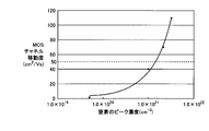
- a large channel mobility about 100 cm 2 / Vs
- the channel mobility may not be sufficiently increased in the above-described MOSFET.
- SiC silicon carbide
- the present invention has been made to solve the above problems, and an object of the present invention is to provide a semiconductor device having excellent electrical characteristics such as channel mobility and a method for manufacturing the same. is there.
- the inventor has completed the present invention as a result of diligent research on the cause of the decrease in channel mobility in order to achieve high channel mobility with high reproducibility in a semiconductor device using SiC as described above. That is, in the above-described semiconductor device, the gate oxide film is formed by dry oxidation, but by such dry oxidation, a trap (interface) is formed at the interface between the gate oxide film and the SiC semiconductor film located under the gate oxide film. Many levels are considered to be formed. The presence of such interface states can be a factor for reducing the above-described channel mobility. This is also estimated from the fact that the threshold voltage of the MOSFET described above is significantly higher than the theoretical value.
- the inventors have found that the channel mobility can be increased by increasing the nitrogen atom concentration or the hydrogen atom concentration in the vicinity of the interface. This is presumably because the influence of the interface state can be suppressed by increasing the nitrogen atom concentration or the hydrogen atom concentration in the vicinity of the interface.
- a semiconductor device in which a semiconductor layer is formed by epitaxial growth on a main surface close to the ⁇ 03-38 ⁇ plane of a substrate made of silicon carbide, and an insulating film (for example, a gate oxide film) is formed on the surface of the semiconductor layer, Carrier mobility in the semiconductor layer near the interface between the semiconductor layer and the insulating film is improved.
- a semiconductor layer and an insulating film are formed on a surface near the (0-33-8) surface, which is the surface on the C (carbon) surface side, among the ⁇ 03-38 ⁇ surfaces, It was found that the mobility was greatly improved.
- the semiconductor device has an off-angle with respect to the (0-33-8) plane in the ⁇ 01-10> direction of ⁇ 3 ° to + 5 °.
- a substrate having a surface and made of silicon carbide, a semiconductor layer formed by epitaxial growth on the main surface of the substrate and made of silicon carbide, and an insulating film formed so as to be in contact with the surface of the semiconductor layer Yes.
- the maximum value of the nitrogen atom concentration in a region within 10 nm from the interface between the semiconductor layer and the insulating film is 1 ⁇ 10 21 cm ⁇ 3 or more.
- a semiconductor device has a main surface having an off angle of ⁇ 3 ° to + 5 ° with respect to the (0-33-8) plane in the ⁇ 01-10> direction, A substrate made of silicon, a semiconductor layer formed by epitaxial growth on the main surface of the substrate and made of silicon carbide, and an insulating film formed in contact with the surface of the semiconductor layer are provided.
- the maximum value of the hydrogen atom concentration in a region within 10 nm from the interface between the semiconductor layer and the insulating film is 1 ⁇ 10 21 cm ⁇ 3 or more.
- a semiconductor device has a main surface with an off angle with respect to the (0-33-8) plane in the ⁇ 01-10> direction being ⁇ 3 ° to + 5 °.
- a substrate made of silicon carbide, a semiconductor layer formed by epitaxial growth on the main surface of the substrate and made of silicon carbide, and an insulating film formed in contact with the surface of the semiconductor layer are provided.
- the maximum value of the total concentration of nitrogen atoms and hydrogen atoms in a region within 10 nm from the interface between the semiconductor layer and the insulating film is 1 ⁇ 10 21 cm ⁇ 3 or more.
- carrier mobility in the semiconductor layer in the vicinity of the interface between the insulating film and the semiconductor layer (for example, channel mobility when the insulating film is used as a gate insulating film) It can be made larger than the case where no hydrogen atom is contained, and an on-resistance lower than that of a conventional semiconductor device using silicon can be realized.
- the carrier mobility can be further increased, and the on-resistance can be further reduced.
- the semiconductor device of the present invention it is possible to obtain a semiconductor device having sufficiently high carrier mobility (channel mobility) and excellent electrical characteristics.
- the (0001) plane of hexagonal single crystal silicon carbide is defined as the silicon plane
- the (000-1) plane is defined as the carbon plane.
- the “off angle with respect to the (0-33-8) plane in the ⁇ 01-10> direction” refers to the above described plane extending in the ⁇ 01-10> direction as a reference for the ⁇ 000-1> direction and the off orientation. This is the angle between the normal projection of the normal of the main surface and the normal of the (0-33-8) plane, and the sign is that the orthogonal projection may approach parallel to the ⁇ 01-10> direction. It is positive and negative when the orthographic projection approaches parallel to the ⁇ 000-1> direction.
- the main surface having an off angle with respect to the (0-33-8) plane in the ⁇ 01-10> direction of not less than ⁇ 3 ° and not more than + 5 ° is a carbon surface satisfying the above conditions in the silicon carbide crystal. Means the side face.
- the (0-33-8) plane includes an equivalent carbon plane-side plane whose expression differs depending on the setting of an axis for defining a crystal plane, and does not include a silicon plane-side plane.
- hydrogen atoms may be contained in the region within 10 nm from the interface between the semiconductor layer and the insulating film.
- nitrogen atoms may be contained in the region within 10 nm from the interface between the semiconductor layer and the insulating film.
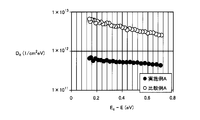
- the interface state density at 0.1 eV below the conduction band is preferably smaller than 1 ⁇ 10 12 cm ⁇ 2 eV ⁇ 1 . Thereby, carrier mobility can be increased more reliably.
- the semiconductor layer may be made of 4H type silicon carbide.
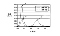
- the ratio of the intensity of the peak appearing near the wavelength of 500 nm to the intensity of the peak appearing near the wavelength of 390 nm is preferably 0.1 or less.
- the on-resistance of the semiconductor device is reduced by reducing the peak appearing in the vicinity of a wavelength of 500 nm in the photoluminescence measurement at room temperature. It was also found that the interface state density can be reduced. More specifically, the peak near the wavelength of 500 nm appears due to the presence of a predetermined stacking fault. The stacking fault corresponding to this peak increases the on-resistance of the semiconductor device, and MOS (Metal- It has been found that the interface state density of the Oxide-Semiconductor structure is increased.
- the peak appearing near the wavelength of 390 nm corresponds to the interband emission of 4H—SiC.
- the peak intensity ratio is 0.1 or less, the on-resistance and interface state density of the semiconductor device can be reduced.
- the ratio of the peak intensities is 0.01 or less, the on-resistance and interface state density of the semiconductor device can be further reduced.
- the state where the peak intensity ratio is 0.1 or less, or 0.01 or less includes the case where the peak intensity ratio is 0. That is, the peak near the wavelength of 500 nm does not have to appear, and most preferably does not appear.
- the method for manufacturing a semiconductor device has a main surface with an off angle of not less than ⁇ 3 ° and not more than + 5 ° with respect to the (0-33-8) plane in the ⁇ 01-10> direction, A step of preparing a substrate made of silicon carbide, a step of forming a semiconductor layer by epitaxial growth on the main surface of the substrate, a step of forming an insulating film in contact with the surface of the semiconductor layer, and the semiconductor layer and the insulating film And a step of adjusting the nitrogen atom concentration so that the maximum value of the nitrogen atom concentration in the region within 10 nm from the interface is 1 ⁇ 10 21 cm ⁇ 3 or more.
- the method for manufacturing a semiconductor device has a main surface with an off angle with respect to the (0-33-8) plane in the ⁇ 01-10> direction of ⁇ 3 ° to + 5 °.
- a step of preparing a substrate made of silicon carbide, a step of forming a semiconductor layer by epitaxial growth on the main surface of the substrate, a step of forming an insulating film in contact with the surface of the semiconductor layer, and the semiconductor layer and the insulating film And a step of adjusting the hydrogen atom concentration so that the maximum value of the hydrogen atom concentration in a region within 10 nm from the interface is 1 ⁇ 10 21 cm ⁇ 3 or more.
- a method for manufacturing a semiconductor device provides a main surface having an off angle of not less than ⁇ 3 ° and not more than + 5 ° with respect to the (0-33-8) plane in the ⁇ 01-10> direction. And a step of preparing a substrate made of silicon carbide, a step of forming a semiconductor layer by epitaxial growth on the main surface of the substrate, a step of forming an insulating film in contact with the surface of the semiconductor layer, and a semiconductor layer, Adjusting the total concentration so that the maximum value of the total concentration of nitrogen atoms and hydrogen atoms in a region within 10 nm from the interface with the insulating film is 1 ⁇ 10 21 cm ⁇ 3 or more.
- the method for manufacturing a semiconductor device may further include a step of containing hydrogen atoms in the region within 10 nm from the interface between the semiconductor layer and the insulating film.
- a step of containing hydrogen atoms in the region within 10 nm from the interface between the semiconductor layer and the insulating film may further include a step of containing hydrogen atoms in the region within 10 nm from the interface between the semiconductor layer and the insulating film.
- the step of containing hydrogen atoms includes the step of heat-treating the substrate on which the insulating film is formed using a gas containing hydrogen atoms as an atmospheric gas. Also good.
- the step of adjusting the nitrogen atom concentration includes a step of heat-treating the substrate on which the insulating film is formed using a gas containing nitrogen atoms as an atmospheric gas. May be included.
- the step of adjusting the nitrogen atom concentration is performed using the inert gas as the atmospheric gas after the step of performing heat treatment using a gas containing nitrogen atoms as the atmospheric gas.
- a step of heat-treating the substrate may be included.
- the method for manufacturing a semiconductor device may further include a step of incorporating nitrogen atoms into the region within 10 nm from the interface between the semiconductor layer and the insulating film.
- a step of incorporating nitrogen atoms into the region within 10 nm from the interface between the semiconductor layer and the insulating film may further include a step of incorporating nitrogen atoms into the region within 10 nm from the interface between the semiconductor layer and the insulating film.
- the step of containing the nitrogen atom includes a step of heat-treating the substrate on which the insulating film is formed using a gas containing a nitrogen atom as an atmospheric gas. May be.
- the step of adjusting the hydrogen atom concentration includes a step of heat-treating the substrate on which the insulating film is formed using a gas containing hydrogen atoms as an atmospheric gas. May be included.
- the step of adjusting the hydrogen atom concentration includes the step of performing a heat treatment using a gas containing hydrogen atoms as the atmospheric gas, and then using the inert gas as the atmospheric gas.
- a step of heat-treating the substrate may be included.
- the gas containing hydrogen atoms may be water vapor or water vapor-containing oxygen.
- hydrogen atoms can be easily introduced in the vicinity of the interface between the semiconductor layer and the insulating film.
- the step of preparing the substrate includes a step of collecting the substrate from a raw crystal made of 4H-type silicon carbide, and another main side opposite to the main surface of the collected substrate. And a step of removing the processing damage layer formed in the region including the surface.
- the on-resistance and interface state density of the semiconductor device are reduced by reducing the peak intensity near the wavelength of 500 nm in the photoluminescence measurement at room temperature. It was found that can be reduced.
- the peak intensity is increased by the following mechanism. Thus, it was found that the on-resistance of the semiconductor device was increased.
- a processing damage layer is formed near the main surface of the substrate.
- the main surface on which the semiconductor layer is formed by epitaxial growth is planarized with high accuracy by polishing or the like.
- the processing damage layer on the semiconductor layer side main surface is removed.
- the processing damage layer near the main surface (back side main surface) opposite to the side on which the semiconductor layer is formed remains.
- a semiconductor layer, an insulating film (oxide film) and the like are formed on the semiconductor-side main surface, and a semiconductor device is manufactured.
- a step of heating to a temperature range of about 1000 ° C. to 1200 ° C. such as thermal oxidation treatment, and a step of passing through the temperature range and heating to a higher temperature range are performed.
- the impurity concentration (for example, nitrogen concentration) in the substrate is high for the purpose of reducing the resistivity of the substrate, a stacking fault is generated from the processing damage layer remaining in the vicinity of the main surface on the back side, and grows inside the substrate. To do.
- the stacking fault grows in the ⁇ 11-20> direction. Therefore, for example, when a general main surface close to the ⁇ 0001 ⁇ plane is adopted as the main surface of the substrate, the stacking fault grown from the processing damage layer grows along the back side main surface, so the semiconductor layer side main surface Will not reach. Therefore, the stacking fault does not propagate to the semiconductor layer formed on the semiconductor layer side main surface. However, when the semiconductor layer side main surface is close to the (0-33-8) plane as in the substrate included in the semiconductor device of the present invention, stacking faults growing from the processing damage layer grow away from the back side main surface. Therefore, it reaches the semiconductor layer side main surface.
- the stacking fault propagates to the semiconductor layer formed on the semiconductor layer side main surface, the peak intensity near the wavelength of 500 nm in the photoluminescence measurement increases, and the on-resistance and interface state density of the semiconductor device increase. To rise.
- the step of preparing the substrate as described above includes the step of removing the processing damage layer, so that the propagation of stacking faults to the semiconductor layer is suppressed, and the on-resistance and interface state density of the semiconductor device are reduced. Can be reduced.
- the substrate in the step of collecting the substrate, the substrate is collected by slicing the raw material crystal, and in the step of removing the processing damage layer, the processing damage formed on the substrate by slicing the raw material crystal. The layer is removed.
- the substrate can be easily collected by slicing the raw crystal. Then, by removing the processing damage layer formed on the substrate by slicing, propagation of stacking faults to the semiconductor layer is suppressed, and the on-resistance and interface state density of the semiconductor device can be reduced.
- the processing damage layer in the step of removing the processing damage layer, may be removed by molten KOH etching.
- the processing damage layer may be removed by dry etching in the step of removing the processing damage layer.
- the processing damage layer in the step of removing the processing damage layer, may be removed by thermal etching.
- the processing damage layer in the step of removing the processing damage layer, may be removed by polishing.
- the processing damage layer can be easily removed by molten KOH etching, dry etching, thermal etching, polishing, or the like.
- the semiconductor device and the manufacturing method thereof of the present invention it is possible to provide a semiconductor device having excellent electrical characteristics such as channel mobility and a manufacturing method thereof.
- FIG. 2 is a flowchart for explaining a method of manufacturing the semiconductor device shown in FIG. It is a cross-sectional schematic diagram for demonstrating each process of the manufacturing method shown in FIG. It is a cross-sectional schematic diagram for demonstrating each process of the manufacturing method shown in FIG. It is a cross-sectional schematic diagram for demonstrating each process of the manufacturing method shown in FIG. It is a cross-sectional schematic diagram for demonstrating each process of the manufacturing method shown in FIG. It is a cross-sectional schematic diagram for demonstrating each process of the manufacturing method shown in FIG. It is a cross-sectional schematic diagram for demonstrating each process of the manufacturing method shown in FIG.
- FIG. 6 is a schematic cross-sectional view illustrating a structure of a semiconductor device in a second embodiment.
- FIG. 9 is a schematic cross-sectional view for illustrating the method for manufacturing the semiconductor device shown in FIG. 8.
- FIG. 9 is a schematic cross-sectional view for illustrating the method for manufacturing the semiconductor device shown in FIG. 8.
- FIG. 9 is a schematic cross-sectional view for illustrating the method for manufacturing the semiconductor device shown in FIG. 8.
- FIG. 9 is a schematic cross-sectional view for illustrating the method for manufacturing the semiconductor device shown in FIG. 8.
- FIG. 6 is a schematic cross-sectional view illustrating a structure of a semiconductor device in a third embodiment.
- 14 is a flowchart for explaining a manufacturing method of the semiconductor device shown in FIG. 13;
- FIG. 10 is a schematic cross-sectional view illustrating the structure of a semiconductor device in a fourth embodiment.
- FIG. 16 is a flowchart for explaining a manufacturing method of the semiconductor device shown in FIG. 15; 17 is a flowchart showing a modification of the method for manufacturing the semiconductor device shown in FIG. 18 is a flowchart showing a second modification of the method for manufacturing the semiconductor device shown in FIG.
- FIG. 6 is a schematic cross sectional view showing a structure of a silicon carbide substrate in a fifth embodiment. It is a flowchart which shows the outline of the manufacturing method of a silicon carbide substrate. 17 is a flowchart showing an outline of a method for manufacturing a silicon carbide substrate in a sixth embodiment.
- FIG. 12 is a schematic cross sectional view for illustrating the method for manufacturing the silicon carbide substrate in the sixth embodiment.
- FIG. 12 is a schematic cross sectional view for illustrating the method for manufacturing the silicon carbide substrate in the sixth embodiment.
- FIG. 12 is a schematic cross sectional view for illustrating the method for manufacturing the silicon carbide substrate in the sixth embodiment.
- FIG. 13 is a schematic cross sectional view showing a structure of a silicon carbide substrate in a seventh embodiment.
- FIG. 22 is a schematic cross sectional view showing a structure of a silicon carbide substrate in an eighth embodiment.
- 20 is a flowchart showing an outline of a method for manufacturing a silicon carbide substrate in an eighth embodiment.
- FIG. 22 is a schematic cross sectional view showing a structure of a silicon carbide substrate in a ninth embodiment.
- 20 is a flowchart showing an outline of a method for manufacturing a silicon carbide substrate in a ninth embodiment.
- FIG. 22 is a schematic cross sectional view showing a structure of a silicon carbide substrate in a tenth embodiment.
- 20 is a flowchart showing an outline of a method for manufacturing a silicon carbide substrate in a tenth embodiment.
- FIG. 22 is a schematic cross sectional view for illustrating the method for manufacturing the silicon carbide substrate in the tenth embodiment. It is a graph which shows the relationship between the peak value of nitrogen atom concentration, and channel mobility. It is a graph which shows the relationship between the peak value of the total concentration of a nitrogen atom and a hydrogen atom, and channel mobility.
- 10 is a schematic cross-sectional view showing a semiconductor device prepared for measurement in Example 5.
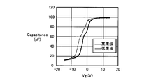
- FIG. It is a graph which shows the CV characteristic about the sample of Example A.
- 6 is a graph showing CV characteristics of a sample of Comparative Example A.
- 10 is a graph showing CV characteristics of the sample of Reference Example A. It is a graph which shows the relationship between the energy at the time of making a conduction band into a reference
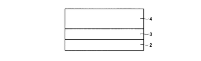
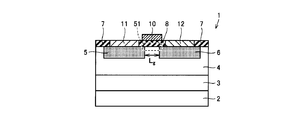
- a semiconductor device 1 shown in FIG. 1 is a lateral MOSFET (Metal-Oxide-Semiconductor Field Effect Transistor) as a semiconductor device, and is formed on a substrate 2 made of 4H-type silicon carbide (SiC).
- MOSFET Metal-Oxide-Semiconductor Field Effect Transistor
- Epitaxial layer 3 made of silicon carbide, p-type layer 4 made of silicon carbide formed on epitaxial layer 3, and an n + region formed at a distance from the region including the surface of p-type layer 4 5, 6 and an oxide film 8 as a gate insulating film located on the channel region between the n + regions 5 and 6, a gate electrode 10 formed on the oxide film 8, an n + region 5, Source electrode 11 and drain electrode 12 formed on each of 6.
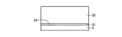
- the substrate 2 is a substrate in which the (0-33-8) plane having an off angle of about 53 ° with respect to the plane orientation ⁇ 0001 ⁇ is the main surface 2A on the epitaxial layer 3 side as a semiconductor layer.
- Substrate 2 contains n-type impurities (impurities that make the conductivity type of substrate 2 n-type; for example, nitrogen).
- Epitaxial layer 3 made of silicon carbide formed on substrate 2 is an undoped layer.
- the p-type layer 4 formed on the epitaxial layer 3 contains a p-type impurity (impurities whose conductivity type of the p-type layer 4 is p-type; for example, aluminum).
- n-type impurities are implanted into the n + regions 5 and 6.
- Oxide films 7 and 8 are formed so as to cover p-type layer 4 and n + regions 5 and 6. Openings are formed in the oxide films 7 and 8 in regions located on the n + regions 5 and 6. Inside the opening, a source electrode 11 and a drain electrode 12 electrically connected to each of the n + regions 5 and 6 are formed.
- a gate electrode 10 is disposed on the oxide film 8 that acts as a gate insulating film.
- the channel length L g which is the distance between the n + regions 5 and 6 can be set to about 100 ⁇ m, for example.
- the channel width may be, for example, about 2 times the channel length L g (about 200 [mu] m).
- the maximum value of the nitrogen atom concentration in the region within 10 nm from the interface between the p-type layer 4 as the semiconductor layer and the oxide film 8 is 1 ⁇ 10 21 cm ⁇ 3 or more.
- the mobility (channel mobility) in the channel region having the channel length L g (the region between the n + regions 5 and 6 in the p-type layer 4) can be made sufficiently large.
- the main surface 2A on the epitaxial layer 3 side of the substrate 2 is a (0-33-8) plane. Therefore, the main surface opposite to the substrate 2 of the p-type layer 4 formed by epitaxial growth and impurity implantation on the main surface 2A is a (0-33-8) plane. As a result, carrier mobility (channel mobility) in the channel region (region including the interface with the oxide film 8 in the n + regions 5 and 6 formed in the p-type layer 4) can be further increased.
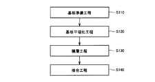
- a silicon carbide substrate preparation step (S10) is performed.
- an n-type conductivity type silicon carbide substrate having a plane orientation (0-33-8) plane as main surface 2A is prepared as substrate 2.
- Such a substrate can be obtained by, for example, a method of cutting a substrate from an ingot (raw material crystal) having a (0001) plane as a main surface so that the (0-33-8) plane is exposed as the main surface 2A. .
- an epitaxial layer forming step (S20) is performed. Specifically, as shown in FIG. 3, undoped silicon carbide epitaxial layer 3 is formed on substrate 2 by epitaxial growth.
- an injection step (S30) is performed. Specifically, first, p-type impurities (for example, aluminum (Al)) are implanted into the epitaxial layer 3 to form the p-type layer 4 as shown in FIG. Next, n + regions 5 and 6 are formed by implanting n-type impurities as shown in FIG. As this n-type impurity, for example, phosphorus (P) can be used. In forming the n + regions 5 and 6, any known method can be used.
- p-type impurities for example, aluminum (Al)
- Al aluminum
- n + regions 5 and 6 are formed by implanting n-type impurities as shown in FIG.
- n-type impurity for example, phosphorus (P) can be used.
- P phosphorus
- an activation annealing process is performed to activate the implanted impurities.
- this activation annealing treatment for example, conditions where the heating temperature is 1700 ° C. and the heating time is 30 minutes may be used.
- a gate insulating film forming step (S40) is performed. Specifically, by oxidizing the upper surfaces of the p-type layer 4 and the n + regions 5 and 6, an oxide film 7 as a gate insulating film is formed as shown in FIG. As the thickness of the oxide film 7, for example, a value of 40 nm can be used.
- a nitrogen annealing step (S50) is performed as shown in FIG. Specifically, heat treatment is performed using nitrogen monoxide (NO) gas as the atmospheric gas.
- NO nitrogen monoxide
- conditions for this heat treatment for example, a condition in which the heating temperature is 1100 ° C. and the heating time is 1 hour can be used.
- nitrogen atoms can be introduced into the interface region between oxide film 7 and p-type layer 4 and n + regions 5 and 6.
- an annealing process using an inert gas for example, an annealing process using argon (Ar) gas as the atmospheric gas is performed. May be.
- an electrode formation step (S60) is performed as shown in FIG. Specifically, a resist film having a pattern is formed on the oxide film 7 by photolithography. Using this resist film as a mask, the oxide film 7 is partially removed to form an opening 15 in a region located above the n + regions 5 and 6. Inside the opening 15, a conductor film to be the source electrode 11 and the drain electrode 12 is formed as shown in FIG. This conductor film is formed with the above-described resist film remaining. Thereafter, the resist film is removed, and the conductive film located on the oxide film 7 is removed (lifted off) together with the resist film, whereby the source electrode 11 and the drain electrode 12 can be formed as shown in FIG. it can. At this time, the oxide film 8 (a part of the oxide film 7 shown in FIG. 6) located between the source electrode 11 and the drain electrode 12 becomes a gate insulating film of the semiconductor device.
- a gate electrode 10 (see FIG. 1) is further formed on the oxide film 8 acting as a gate insulating film.
- the following method can be used. For example, a resist film having an opening pattern located in a region on the oxide film 8 is formed in advance, and a conductor film constituting the gate electrode is formed so as to cover the entire surface of the resist film. Then, by removing the resist film, the conductor film other than the portion of the conductor film to be the gate electrode is removed (lifted off). As a result, the gate electrode 10 is formed as shown in FIG. In this way, the semiconductor device 1 as shown in FIG. 1 can be obtained.
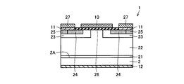
- the semiconductor device 1 is a vertical DiMOSFET (Double Implanted MOSFET), and includes a substrate 2, a buffer layer 21, a breakdown voltage holding layer 22, a p region 23, an n + region 24, a p + region 25, and an oxide film. 26, the source electrode 11 and the upper source electrode 27, the gate electrode 10, and the drain electrode 12 formed on the back surface side of the substrate 2.
- buffer layer 21 made of silicon carbide is formed on main surface 2A of substrate 2 made of silicon carbide of n-type conductivity.
- Buffer layer 21 is n-type in conductivity type and has a thickness of 0.5 ⁇ m, for example.
- the concentration of the n-type impurity in the buffer layer 21 can be set to 5 ⁇ 10 17 cm ⁇ 3 , for example.
- a breakdown voltage holding layer 22 is formed on the buffer layer 21.
- the breakdown voltage holding layer 22 is made of silicon carbide of n-type conductivity, and has a thickness of 10 ⁇ m, for example. Further, as the concentration of the n-type impurity in the breakdown voltage holding layer 22, for example, a value of 5 ⁇ 10 15 cm ⁇ 3 can be used.
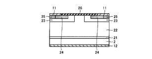
- p regions 23 having a p-type conductivity are formed at intervals.
- n + region 24 is formed in a region including the main surface of p region 23.
- a p + region 25 is formed at a position adjacent to the n + region 24.
- An oxide film 26 is formed so as to extend up to.
- a gate electrode 10 is formed on the oxide film 26.
- the source electrode 11 is formed so as to be in contact with the n + region 24 and the p + region 25.
- An upper source electrode 27 is formed on the source electrode 11.
- the drain electrode 12 is formed on the main surface (back surface) opposite to the main surface on which the buffer layer 21 is formed.
- the maximum value of the nitrogen atom concentration in a region within 10 nm from the interface between the oxide film 26 and the n + region 24, p + region 25, p region 23, and breakdown voltage holding layer 22 as a semiconductor layer is 1 ⁇ 10 It is 21 cm ⁇ 3 or more.
- the mobility of the channel region under the oxide film 26 (part of the p region 23 that is in contact with the oxide film 26 and between the n + region 24 and the breakdown voltage holding layer 22) is shown in FIG. Improvements can be made in the same manner as in the case of the semiconductor device 1.
- the main surface 2A on the buffer layer 21 side of the substrate 2 is a (0-33-8) plane. Therefore, the main surface opposite to the substrate 2 of the p region 23 formed by epitaxial growth and impurity implantation on the main surface 2A is a (0-33-8) plane. As a result, carrier mobility (channel mobility) in the channel region can be further increased.
- a method for manufacturing the semiconductor device 1 shown in FIG. 8 will be described with reference to FIGS.
- a silicon carbide substrate preparation step S10 is performed.
- substrate 2 (see FIG. 9) made of silicon carbide having (0-33-8) plane as the main surface is prepared in the same manner as in the method of manufacturing the semiconductor device in the first embodiment.
- the substrate 2 for example, a substrate having an n-type conductivity and a substrate resistance of 0.02 ⁇ cm may be used as the substrate 2 (see FIG. 9).
- buffer layer 21 is formed on main surface 2 ⁇ / b> A of substrate 2.
- an epitaxial layer made of silicon carbide of n-type conductivity for example, having a thickness of 0.5 ⁇ m is formed.
- a value of 5 ⁇ 10 17 cm ⁇ 3 can be used as the impurity concentration in the buffer layer 21.
- a breakdown voltage holding layer 22 is formed on the buffer layer 21 as shown in FIG.
- a layer made of silicon carbide of n-type conductivity is formed by an epitaxial growth method.
- a value of 10 ⁇ m can be used as the thickness of the breakdown voltage holding layer 22.
- concentration of the n-type conductive impurity in the breakdown voltage holding layer 22 for example, a value of 5 ⁇ 10 15 cm ⁇ 3 can be used.
- an implantation step (S30) is performed in the same manner as the step shown in FIG. Specifically, by using an oxide film formed by photolithography and etching as a mask, an impurity having a conductivity type of p-type is implanted into the breakdown voltage holding layer 22, thereby forming the p region 23 as shown in FIG. Form. Further, after removing the used oxide film, an oxide film having a new pattern is formed again by photolithography and etching. Then, using the oxide film as a mask, an n-type impurity is implanted into a predetermined region, thereby forming an n + region 24. Further, the p + region 25 is formed by implanting an impurity having a p-type conductivity by a similar method. As a result, a structure as shown in FIG. 10 is obtained.
- activation annealing is performed.
- this activation annealing treatment for example, argon gas is used as an atmospheric gas, and conditions such as a heating temperature of 1700 ° C. and a heating time of 30 minutes can be used.
- a gate insulating film forming step (S40) is performed as in the step shown in FIG. Specifically, as illustrated in FIG. 11, an oxide film 26 is formed so as to cover the breakdown voltage holding layer 22, the p region 23, the n + region 24, and the p + region 25.
- the oxide film 26 may be formed by dry oxidation (thermal oxidation), for example.
- dry oxidation thermal oxidation
- conditions for this dry oxidation conditions such as a heating temperature of 1200 ° C. and a heating time of 30 minutes can be used.
- a nitrogen annealing step (S50) is performed as in the step shown in FIG. Specifically, the annealing process is performed using nitrogen monoxide (NO) as the atmosphere gas.
- NO nitrogen monoxide
- the heating temperature is 1100 ° C. and the heating time is 120 minutes.
- nitrogen atoms are introduced near the interface between the oxide film 26 and the underlying breakdown voltage holding layer 22, p region 23, n + region 24, and p + region 25.
- annealing using nitrogen monoxide as an atmospheric gas annealing using nitrogen monoxide as an atmospheric gas.
- argon (Ar) gas which is an inert gas may be performed.
- argon gas may be used as the atmosphere gas
- the heating temperature may be 1100 ° C. and the heating time may be 60 minutes.
- an electrode formation step (S60) is performed in the same manner as the step shown in FIG. Specifically, a resist film having a pattern is formed on the oxide film 26 by using a photolithography method. Then, using the resist film as a mask, portions of the oxide film located on the n + region 24 and the p + region 25 are removed by etching. Thereafter, on the resist film, in the opening formed in the oxide film 26, the region in contact with the n + region 24 and the p + region 25, and the main surface opposite to the buffer layer 21 of the substrate 2, A conductor film such as metal is formed. Thereafter, by removing the resist film, the conductor film located on the resist film is removed (lifted off).
- nickel (Ni) can be used as the conductor.
- the source electrode 11 and the drain electrode 12 can be obtained as shown in FIG.
- Ar argon
- a semiconductor device 1 according to the present invention basically has the same configuration as that of the semiconductor device 1 shown in FIG. 1, but an interface between a p-type layer 4 as a semiconductor layer and an oxide film 8. 1 differs from the semiconductor device 1 shown in FIG. 1 in that the maximum value of the hydrogen atom concentration is 1 ⁇ 10 21 cm ⁇ 3 or more in the boundary region 41 including the region within 10 nm from the region. Even in this case, similarly to the semiconductor device shown in FIG. 1, the mobility (channel mobility) in the channel region including the boundary region 41 can be set to a sufficiently large value. In the semiconductor device 1 shown in FIG.
- the hydrogen atoms contained in the boundary region 41 are in a region within 10 nm from the interface between the p-type layer 4 and the oxide film 8 of the semiconductor device 1 shown in FIG. 1. This is presumably because the interface state is reduced similarly to the nitrogen atom contained.
- the manufacturing method of the semiconductor device shown in FIG. 14 is basically the same as the manufacturing method of the semiconductor device shown in FIG. 2, but a hydrogen annealing step (S70) is performed instead of the nitrogen annealing step (S50) in FIG. Different points are implemented. Specifically, the silicon carbide substrate preparation step (S10), the epitaxial layer formation step (S20), the implantation step (S30), and the gate insulating film formation step (S40) are performed in the same manner as the manufacturing method shown in FIG. . Thereafter, a hydrogen annealing step (S70) is performed. Specifically, heat treatment is performed using hydrogen gas (H 2 ) gas as the atmosphere gas.
- H 2 hydrogen gas
- a condition in which the heating temperature is 1100 ° C. and the heating time is 1 hour can be used.
- hydrogen atoms can be introduced into the interface region between oxide film 7 and p-type layer 4 and n + regions 5 and 6.
- an annealing process using an inert gas for example, an annealing process using argon (Ar) gas as the atmosphere gas is performed. May be.
- water vapor or water vapor-containing oxygen gas may be used as the atmospheric gas instead of hydrogen gas.
- the semiconductor device 1 shown in FIG. 13 can be obtained by performing the electrode forming step (S60) in the same manner as the manufacturing method shown in FIG.
- semiconductor device 1 in the present embodiment basically has the same configuration as that of semiconductor device 1 shown in FIG. 1, but includes p-type layer 4 as a semiconductor layer, oxide film 8, and the like.
- the maximum value of the total concentration of nitrogen atoms and hydrogen atoms is 1 ⁇ 10 21 cm ⁇ 3 or more in the boundary region 51 including the region within 10 nm from the interface of Yes.
- the mobility (channel mobility) in the channel region including the boundary region 41 can be set to a sufficiently large value.
- the manufacturing method of the semiconductor device shown in FIG. 16 is basically the same as the manufacturing method of the semiconductor device shown in FIG. 2, but after the nitrogen annealing step (S50) in FIG.
- the hydrogen annealing step (S70) is performed before ().
- a silicon carbide substrate preparation step (S10), an epitaxial layer formation step (S20), an implantation step (S30), a gate insulating film formation step (S40), nitrogen annealing Step (S50) is performed.
- a hydrogen annealing step (S70) is performed.
- this step (S70) the same conditions (annealing conditions using hydrogen gas) as in the hydrogen annealing step (S70) in the manufacturing method of Embodiment 3 can be used.
- nitrogen atoms and hydrogen atoms can be introduced into the interface region between oxide film 7 and p-type layer 4 and n + regions 5 and 6.
- water vapor or water vapor-containing oxygen gas may be used as the atmospheric gas instead of hydrogen gas.
- the hydrogen annealing step (S70) may be performed prior to the nitrogen annealing step (S50).
- the hydrogen annealing step (S70) and the nitrogen annealing step (S50) may be performed simultaneously by performing a heat treatment using an atmosphere gas containing hydrogen atoms and nitrogen atoms.
- the semiconductor device 1 shown in FIG. 15 can be obtained by performing the electrode forming step (S60) in the same manner as the manufacturing method shown in FIG.
- the manufacturing method of the semiconductor device shown in FIG. 17 is basically the same as the manufacturing method of the semiconductor device shown in FIG. 16, but after the hydrogen annealing step (S70) in FIG. ) Is different in that a post heat treatment step (S80) is performed.
- a silicon carbide substrate preparation step (S10), an epitaxial layer formation step (S20), an implantation step (S30), a gate insulating film formation step (S40), nitrogen annealing A process (S50) and a hydrogen annealing process (S70) are performed. Thereafter, a post heat treatment step (S80) is performed.
- an annealing process using an inert gas is performed.
- an inert gas for example, argon (Ar)
- the heating temperature is 1100 ° C.
- the heating time is 60 minutes.
- the semiconductor device 1 shown in FIG. 15 can be obtained by performing the electrode forming step (S60) in the same manner as the manufacturing method shown in FIG.
- a heat treatment step similar to the above-described post heat treatment step (S80) may be additionally performed between the nitrogen annealing step (S50) and the hydrogen annealing step (S70).
- the hydrogen annealing step (S70) may be performed prior to the nitrogen annealing step (S50).
- the hydrogen annealing step (S70) and the nitrogen annealing step (S50) may be performed simultaneously by performing a heat treatment using an atmosphere gas containing hydrogen atoms and nitrogen atoms.
- the manufacturing method of the semiconductor device shown in FIG. 18 is basically the same as the manufacturing method of the semiconductor device shown in FIG. 17, but is different from the manufacturing method shown in FIG. 17 in the silicon carbide substrate preparation step.
- the silicon carbide substrate preparation step in the present modification includes a raw material crystal preparation step (S11), a slicing step (S12), and a processing damage layer removal step (S13). It is out.
- a raw material crystal made of 4H type silicon carbide is produced, for example, by a sublimation method.
- step (S12) the raw material crystal produced in step (S11) is sliced, and substrate 2 is collected. At this time, the raw material is such that one main surface of the substrate 2 is a (0-33-8) plane (carbon surface side surface) and the other main surface is a (03-38) surface (silicon surface side surface). Crystals are sliced.
- step (S13) at least the (03-38) plane processing damage layer is removed from the processing damage layers formed in the region including the main surfaces on both sides of the substrate 2 by slicing in step (S12).
- This processing damage layer can be removed by, for example, etching treatment such as molten KOH etching, dry etching, thermal etching, or polishing.
- the main surface on the (0-33-8) plane side on which an epitaxial layer is to be formed in a later step is a surface suitable for epitaxial growth by combining mechanical polishing (MP), chemical mechanical polishing (CMP), etc. The surface is flattened to be rough.
- the processing damage layer is also removed from the region including the main surface on the (0-33-8) plane side.
- the region including the main surface on the (0-33-8) plane side may be subjected to the above planarization after the processing damage layer is removed in the same manner as the (03-38) plane side. .
- the epitaxial layer forming step (S20), the implantation step (S30), the gate insulating film forming step (S40), and the nitrogen annealing step By performing the S50), the hydrogen annealing step (S70), the post heat treatment step (S80), and the electrode formation step (S60), the semiconductor device according to the second modification is obtained.
- the processing damage layer introduced into the region including the (03-38) surface of the substrate 2 in the step (S12) is removed in the step (S13). Further, the processing damage layer introduced into the region including the (0-33-8) plane of the substrate 2 is removed in a polishing process such as MP or CMP. Therefore, the growth of stacking faults from the processing damage layer in the process such as the gate insulating film forming step (S40) heated to about 1000 ° C. to 1200 ° C. is suppressed.
- the lateral MOSFET is shown as the semiconductor device 1, but the features of the third and fourth embodiments may be applied to the vertical DiMOSFET shown in FIG. That is, in the semiconductor device 1 shown in FIG. 8, hydrogen atoms in a region within 10 nm from the interface between the oxide film 26 and the n + region 24, the p + region 25, the p region 23, and the breakdown voltage holding layer 22 as semiconductor layers.
- the maximum value of the concentration or the maximum value of the total concentration of nitrogen atoms and hydrogen atoms can be 1 ⁇ 10 21 cm ⁇ 3 or more.
- the main surface 2A on the semiconductor side of the substrate 2 can be a (0-33-8) plane.
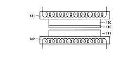
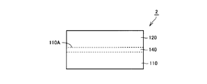
- the semiconductor device according to the present embodiment has basically the same structure as the semiconductor device according to the first to fourth embodiments and has the same effects. However, the semiconductor device according to the present embodiment is different from the first to fourth embodiments in the structure of the substrate 2.
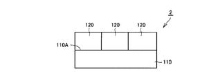
- substrate 2 constituting semiconductor device 1 in the present embodiment includes base layer 110 made of silicon carbide and single crystal silicon carbide, and is arranged on one main surface 110 ⁇ / b> A of base layer 110.
- SiC layer 120 formed.
- Base layer 110 and SiC layer 120 are made of different crystals.
- the defect density of SiC layer 120 is smaller than the defect density of base layer 110.
- High-quality silicon carbide single crystal is difficult to increase in diameter.
- a substrate having a predetermined shape and size is required. Therefore, even when a high-quality silicon carbide single crystal (for example, a silicon carbide single crystal having a low defect density) is obtained, a region that cannot be processed into a predetermined shape by cutting or the like may not be used effectively.
- substrate 2 constituting the semiconductor device of the present embodiment includes base layer 110 made of silicon carbide and SiC layer 120 made of single crystal silicon carbide and disposed on base layer 110.
- the defect density of the SiC layer 120 is smaller than the defect density of the base layer 110. Therefore, the base substrate 110 made of silicon carbide crystal having a high defect density and low quality is processed into the predetermined shape and size to form the base layer 110, and the desired shape of the high quality on the base layer 110 is obtained.
- a silicon carbide single crystal in which the above is not realized can be arranged as SiC layer 120. Since the substrate 2 obtained in this way is unified in a predetermined shape and size, the production of the semiconductor device 1 can be made efficient.
- the silicon carbide substrate obtained in this way can manufacture semiconductor device 1 using high quality SiC layer 120, a silicon carbide single crystal can be used effectively.
- a semiconductor device capable of reducing the manufacturing cost can be provided.
- the half width of the X-ray rocking curve of the SiC layer 120 may be smaller than the half width of the X-ray rocking curve of the base layer 110.
- the impurity concentration of the base layer 110 is higher than 2 ⁇ 10 19 cm ⁇ 3
- the impurity concentration of the SiC layer 120 is higher than 5 ⁇ 10 18 cm ⁇ 3 and lower than 2 ⁇ 10 19 cm ⁇ 3. Also good.
- the impurity concentration is less than 2 ⁇ 10 19 cm ⁇ 3 , generation of stacking faults due to heat treatment (for example, thermal oxidation treatment) in the semiconductor device manufacturing process is suppressed.
- heat treatment for example, thermal oxidation treatment
- it exceeds 2 ⁇ 10 19 cm ⁇ 3 it is difficult to suppress stacking faults. Therefore, when the impurity concentration exceeds 2 ⁇ 10 19 cm ⁇ 3 , it is preferable to perform the step of removing the processing damage layer as in the second modification of the fourth embodiment.
- impurity concentration in the substrate 2 made of silicon carbide is 2 ⁇ 10 19 cm -3, with small layer provided (base layer 110) resistivity, impurity concentration is smaller than 2 ⁇ 10 19 cm -3
- the layer (SiC layer 120) By disposing the layer (SiC layer 120) on the base layer 110, even if heat treatment in the device manufacturing process is subsequently performed, at least the SiC layer 120 causes stacking faults and the processing damage layer is removed. It can suppress without doing.
- the semiconductor device 1 by forming an epitaxially grown layer (active layer) made of SiC on the SiC layer 120 to produce the semiconductor device 1, while reducing the resistivity of the silicon carbide substrate 2 due to the presence of the base layer 110, It is possible to suppress the influence of stacking faults that may occur in the base layer 110 from affecting the characteristics of the semiconductor device.
- the impurity concentration of the SiC layer 120 is 5 ⁇ 10 18 cm ⁇ 3 or less, the resistivity of the SiC layer 120 becomes too high, so that the vertical semiconductor device (in the thickness direction of the substrate 2) as shown in FIG. There may be a problem that the substrate 2 suitable for a semiconductor device through which a current flows cannot be obtained.
- the impurity concentration of the base layer 110 is higher than 2 ⁇ 10 19 cm ⁇ 3
- the impurity concentration of the SiC layer 120 is higher than 5 ⁇ 10 18 cm ⁇ 3 and lower than 2 ⁇ 10 19 cm ⁇ 3.
- the micropipe density of the SiC layer 120 is smaller than the micropipe density of the base layer 110.
- the threading screw dislocation density of SiC layer 120 is preferably smaller than the threading screw dislocation density of base layer 110.
- the threading edge dislocation density of SiC layer 120 is preferably smaller than the threading edge dislocation density of base layer 110.
- the basal plane dislocation density of SiC layer 120 is preferably smaller than the basal plane dislocation density of base layer 110.
- the mixed dislocation density of SiC layer 120 is preferably smaller than the mixed dislocation density of base layer 110.
- the stacking fault density of SiC layer 120 is preferably smaller than the stacking fault density of base layer 110.
- the point defect density of SiC layer 120 is preferably smaller than the point defect density of base layer 110.
- the SiC layer in which the defect density such as the micropipe density, the threading screw dislocation density, the threading edge dislocation density, the basal plane dislocation density, the mixed dislocation density, the stacking fault density, and the point defect density is reduced as compared with the base layer 110.
- a high-quality active layer epitaxial growth layer
- the base layer 110 and the SiC layer 120 are bonded, for example. Thereby, silicon carbide substrate 2 on which SiC layer 120 is arranged can be easily obtained while suppressing the propagation of defects in base layer 110. At this time, the base layer 110 and the SiC layer 120 may be joined directly, or may be joined via an intermediate layer.
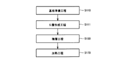
- a substrate preparation step is first performed as a step (S110).
- step (S110) referring to FIG. 19, for example, base substrate 110 made of single crystal silicon carbide and SiC substrate 120 made of single crystal silicon carbide are prepared.
- main surface 120A of SiC substrate 120 is the main surface of substrate 2 obtained by this manufacturing method, so the plane orientation of main surface 120A of SiC substrate 120 is selected in accordance with the plane orientation of the desired main surface.
- SiC substrate 120 whose main surface is a (0-33-8) plane is prepared.
- the base substrate 110 for example, a substrate having an impurity concentration higher than 2 ⁇ 10 19 cm ⁇ 3 is employed.
- SiC substrate 120 for example, a substrate having an impurity concentration larger than 5 ⁇ 10 18 cm ⁇ 3 and smaller than 2 ⁇ 10 19 cm ⁇ 3 is employed.
- a substrate flattening step is performed as a step (S120).
- This step (S120) is not an essential step, but can be performed when the flatness of the base substrate 110 and the SiC substrate 120 prepared in the step (S110) is insufficient. Specifically, for example, the main surface of base substrate 110 or SiC substrate 120 is polished. On the other hand, the manufacturing cost can be reduced by omitting this step.
- an etching process may be performed to remove a processing damage layer formed in a region including the main surface when the SiC substrate 120 is collected from the raw crystal (ingot). The etching process can be performed by, for example, molten KOH etching.
- a stacking step is performed.
- base substrate 110 and SiC substrate 120 are stacked so that their main surfaces 110A and 120B are in contact with each other, and a laminated substrate is manufactured.
- a joining step is performed as a step (S140).
- step (S140) base substrate 110 and SiC substrate 120 are joined by heating the laminated substrate to a temperature range equal to or higher than the sublimation temperature of silicon carbide, for example.
- substrate 2 including base layer 110 and SiC layer 120 is completed.
- this substrate 2 is used, and the semiconductor device 1 is manufactured in the same manner as in the first to fourth embodiments.
- the heating temperature of the multilayer substrate in the step (S140) is preferably 1800 ° C. or higher and 2500 ° C. or lower.
- the heating temperature is lower than 1800 ° C., it takes a long time to join base substrate 110 and SiC substrate 120, and the manufacturing efficiency of substrate 2 decreases.
- the heating temperature exceeds 2500 ° C., the surfaces of the base substrate 110 and the SiC substrate 120 are roughened, and there is a possibility that the generation of defects in the manufactured substrate 2 increases.
- the heating temperature of the laminated substrate in the step (S140) is preferably 1900 ° C. or higher and 2100 ° C. or lower.
- the pressure of the atmosphere in the heating in the step (S140) is 10 ⁇ 5 Pa to 10 6 Pa, more preferably 10 ⁇ 2 Pa to 10 4 Pa, so that the above bonding is performed with a simple apparatus. can do.
- the atmosphere at the time of a heating in a process (S140) is an inert gas atmosphere.
- the atmosphere is more preferably an inert gas atmosphere containing at least one selected from the group consisting of argon, helium and nitrogen.
- FIGS. 6 Next, as a sixth embodiment, another method for manufacturing a substrate constituting the semiconductor device of the present invention will be described with reference to FIGS.
- the substrate manufacturing method according to the sixth embodiment is basically performed in the same manner as in the fifth embodiment. However, the substrate manufacturing method in the sixth embodiment is different from that in the fifth embodiment in the formation process of the base layer 110.
- a substrate preparation step is first performed as a step (S110).
- SiC substrate 120 is prepared in the same manner as in the fifth embodiment, and source substrate 111 made of silicon carbide is prepared.
- Raw material substrate 111 may be made of single crystal silicon carbide, may be made of polycrystalline silicon carbide, or may be a sintered body of silicon carbide. Further, a raw material powder made of silicon carbide can be employed instead of the raw material substrate 111.
- a proximity placement step is performed as a step (S150).
- SiC substrate 120 and raw material substrate 111 are held by first heater 181 and second heater 182 arranged to face each other.
- SiC substrate 120 and raw material substrate 111 are arranged close to each other so that main surface 120B and main surface 111A as the main surfaces face each other at an interval of 1 ⁇ m or more and 1 cm or less, for example, an interval of about 1 mm. Is done.
- a sublimation step is performed as a step (S160).
- SiC substrate 120 is heated to a predetermined substrate temperature by first heater 181.
- the raw material substrate 111 is heated to a predetermined raw material temperature by the second heater 182.
- SiC is sublimated from the surface of the source substrate by heating source substrate 111 to the source temperature.
- the substrate temperature is set lower than the raw material temperature. Specifically, for example, the substrate temperature is set to be 1 ° C. or more and 100 ° C. or less lower than the raw material temperature.
- the substrate temperature is, for example, 1800 ° C. or higher and 2500 ° C. or lower.
- SiC sublimated from the raw material substrate 111 reaches a surface of the SiC substrate 120 and becomes a solid, thereby forming the base layer 110.
- all of the SiC constituting the raw material substrate 111 is sublimated and moves onto the surface of the SiC substrate 120.
- the step (S160) is completed, and the substrate 2 shown in FIG. 19 is completed.
- Embodiment 7 which is still another embodiment of the present invention will be described.
- the semiconductor device according to the seventh embodiment basically has the same structure as that of the fifth embodiment. However, the semiconductor device of the seventh embodiment is different from that of the fifth embodiment in the manufacturing method.
- a substrate having a structure different from that in the fifth embodiment is prepared in the silicon carbide substrate preparation step performed as step (S10).
- a plurality of SiC layers 120 are arranged side by side in plan view. That is, a plurality of SiC layers 120 are arranged along main surface 110 ⁇ / b> A of base layer 110. More specifically, the plurality of SiC layers 120 are arranged in a matrix so that adjacent SiC layers 120 on base layer 110 are in contact with each other.
- substrate 2 in the present embodiment is substrate 2 that can be handled as a large-diameter substrate having high-quality SiC layer 120.
- the manufacturing process of the semiconductor device can be made efficient.
- the substrate 2 in the seventh embodiment is implemented by arranging a plurality of SiC substrates 120 in a plane on the base substrate 110 in the step (S130) in the fifth embodiment (see FIG. 19) or
- the first heater 181 holds the plurality of SiC substrates 120 in a state of being arranged in a plane (see FIG. 22). Can be produced in the same manner.
- the substrate 2 is used and the semiconductor device 1 is manufactured.
- the semiconductor device 1 is manufactured by forming a plurality of semiconductor layers on the SiC layer 120 of the substrate 2 shown in FIG. At this time, each semiconductor device 1 is manufactured so as not to cross the boundary region between adjacent SiC layers 120.
- the semiconductor device 1 according to the eighth embodiment basically has the same structure as the semiconductor device 1 according to the fifth embodiment, and has the same effects. However, the semiconductor device 1 of the eighth embodiment is different from that of the fifth embodiment in the structure of the substrate 2.
- amorphous SiC layer 140 as an intermediate layer made of amorphous SiC is arranged between base layer 110 and SiC layer 120.
- Base layer 110 and SiC layer 120 are connected by amorphous SiC layer 140. Due to the presence of the amorphous SiC layer 140, for example, the substrate 2 in which the base layer 110 and the SiC layer 120 having different impurity concentrations are stacked can be easily manufactured.
- a substrate preparation step is performed as step (S110) in the same manner as in the fifth embodiment, and base substrate 110, SiC substrate 120, Is prepared.
- a Si layer forming step is performed as a step (S111).
- an Si layer having a thickness of, for example, about 100 nm is formed on one main surface of base substrate 110 prepared in step (S110).
- the Si layer can be formed by, for example, a sputtering method.
- step (S130) SiC substrate 120 prepared in step (S110) is placed on the Si layer formed in step (S111). Thereby, a laminated substrate in which the SiC substrate 120 is laminated on the base substrate 110 with the Si layer interposed therebetween is obtained.
- a heating step is performed as a step (S170).
- the laminated substrate produced in the step (S130) is heated to about 1500 ° C. in a mixed gas atmosphere of hydrogen gas and propane gas having a pressure of 1 ⁇ 10 3 Pa, for example, for about 3 hours. Retained.
- carbon is supplied to the Si layer mainly by diffusion from the base substrate 110 and the SiC substrate 120, and an amorphous SiC layer 140 is formed as shown in FIG.
- substrate 2 in the eighth embodiment in which base layer 110 and SiC layer 120 having different impurity concentrations are connected by amorphous SiC layer 140 can be easily manufactured.
- Embodiment 9 which is still another embodiment of the present invention will be described.
- the semiconductor device 1 according to the ninth embodiment basically has the same structure as the semiconductor device 1 according to the fifth embodiment, and has the same effects. However, the semiconductor device 1 of the ninth embodiment is different from that of the fifth embodiment in the structure of the substrate 2.
- substrate 2 in the ninth embodiment ohmic as an intermediate layer formed by siliciding at least a part of a metal layer between base layer 110 and SiC layer 120.
- the contact layer 150 is different from the fifth embodiment in that the contact layer 150 is formed.
- Base layer 110 and SiC layer 120 are connected by ohmic contact layer 150. Due to the presence of the ohmic contact layer 150, for example, the substrate 2 in which the base layer 110 and the SiC layer 120 having different impurity concentrations are stacked can be easily manufactured.
- a substrate preparation step is performed as step (S110) in the same manner as in the fifth embodiment, and base substrate 110, SiC substrate 120, Is prepared.
- a metal film forming step is performed as a step (S112).
- a metal film is formed, for example, by vapor-depositing metal on one main surface of the base substrate 110 prepared in the step (S110).
- This metal film contains, for example, at least one selected from metals that form silicide when heated, for example, nickel, molybdenum, titanium, aluminum, and tungsten.
- step (S130) SiC substrate 120 prepared in step (S110) is placed on the metal film formed in step (S112). Thereby, a laminated substrate is obtained in which SiC substrate 120 is laminated on base substrate 110 with a metal film interposed therebetween.
- a heating step is performed as a step (S170).
- the multilayer substrate manufactured in step (S130) is heated to about 1000 ° C. in an inert gas atmosphere such as argon.
- an inert gas atmosphere such as argon.
- the metal film the region in contact with the base substrate 110 and the region in contact with the SiC substrate
- the ohmic contact layer 150 that makes ohmic contact with the base layer 110 and the SiC layer 120 is formed.
- substrate 2 in the ninth embodiment in which base layer 110 and SiC layer 120 having different impurity concentrations are connected by ohmic contact layer 150 can be easily manufactured.
- Embodiment 10 which is still another embodiment of the present invention will be described.
- the semiconductor device 1 according to the tenth embodiment basically has the same structure as the semiconductor device 1 according to the fifth embodiment, and has the same effects. However, the semiconductor device 1 according to the tenth embodiment is different from the fifth embodiment in the structure of the substrate 2.
- carbon layer 160 as an intermediate layer is formed between base layer 110 and SiC layer 120. It is different from the case. Base layer 110 and SiC layer 120 are connected by carbon layer 160. Due to the presence of the carbon layer 160, for example, the substrate 2 in which the base layer 110 and the SiC layer 120 having different impurity concentrations are stacked can be easily manufactured.
- step (S110) is performed in the same manner as in the fifth embodiment, and then step (S120) is performed in the same manner as in the fifth embodiment as necessary.
- a carbon adhesive is applied onto the main surface of base substrate 110, whereby precursor layer 161 is formed.
- a carbon adhesive what consists of resin, graphite fine particles, and a solvent can be employ
- the resin a resin that becomes non-graphitizable carbon when heated, such as a phenol resin, can be employed.
- the solvent for example, phenol, formaldehyde, ethanol, or the like can be used.
- the coating amount of the carbon adhesive is preferably 10 mg / cm 2 or more and 40 mg / cm 2 or less, and more preferably 20 mg / cm 2 or more and 30 mg / cm 2 or less.
- the thickness of the carbon adhesive to be applied is preferably 100 ⁇ m or less, and more preferably 50 ⁇ m or less.
- a stacking step is performed.
- SiC substrate 120 is placed in contact with precursor layer 161 formed in contact with the main surface of base substrate 110, and the laminated substrate is Produced.
- a pre-baking step is performed.
- the solvent component is removed from the carbon adhesive constituting the precursor layer 161 by heating the laminated substrate.
- the multilayer substrate is gradually heated to a temperature range exceeding the boiling point of the solvent component while applying a load to the multilayer substrate in the thickness direction. This heating is preferably performed while the base substrate 110 and the SiC substrate 120 are pressure-bonded using a clamp or the like. Further, by performing pre-baking (heating) as much as possible, degassing from the adhesive proceeds, and the strength of bonding can be improved.
- a firing step is performed as a step (S190).
- the laminated substrate heated in the step (S180) and pre-baked with the precursor layer 161 is heated to a high temperature, preferably 900 ° C. to 1100 ° C., for example, 1000 ° C., preferably 10 minutes to 10 minutes.
- the precursor layer 161 is fired by being held for a period of time, for example, 1 hour.
- an atmosphere at the time of firing an inert gas atmosphere such as argon is adopted, and the pressure of the atmosphere can be set to atmospheric pressure, for example.
- the precursor layer 161 becomes the carbon layer 160 made of carbon.
- substrate 2 in the tenth embodiment in which base substrate (base layer) 10 and SiC substrate (SiC layer) 20 are bonded by carbon layer 160 is obtained.
- a semiconductor device 1 according to the present invention has a main surface having an off angle of ⁇ 3 ° to + 5 ° with respect to the (0-33-8) plane in the ⁇ 01-10> direction, and is a substrate 2 made of silicon carbide. And a semiconductor layer (p-type layer 4 in FIG. 1 and p region 23 in FIG. 8) and an insulating film (oxide film 8 in FIG. 1 and oxide film 26 in FIG. 8).
- the semiconductor layer (p-type layer 4, p region 23) is formed on substrate 2 and is made of silicon carbide.
- the insulating films (oxide films 8 and 26) are formed in contact with the surface of the semiconductor layer (p-type layer 4 including channel region, p region 23).
- the maximum value of the nitrogen atom concentration in a region within 10 nm from the interface between the semiconductor layer and the insulating film (interface between the channel region and the oxide films 8 and 26) is 1 ⁇ 10 21 cm ⁇ 3 or more.
- the carrier mobility (channel mobility) in the channel region in the vicinity of the interface between the oxide films 8 and 26 acting as the gate insulating film and the channel region is not included in the vicinity of the interface. It is possible to realize a lower on-resistance than a conventional semiconductor device using silicon. For this reason, it is possible to obtain a semiconductor device 1 that exhibits sufficiently large channel mobility and excellent electrical characteristics.
- the maximum value of the nitrogen atom concentration is set to 1 ⁇ 10 21 cm ⁇ 3 or more because the channel mobility is a practically sufficient value by setting the nitrogen atom concentration to the above value or more. It is because it can be set to 2 / Vs or more.
- hydrogen atoms are contained in a region within 10 nm from the interface between the semiconductor layer (p-type layer 4 in FIG. 1 and p region 23 in FIG. 8) and the insulating film (oxide films 8 and 26). May be. In this case, the interface state in the region can be more reliably reduced.
- a semiconductor device 1 according to the present invention has a main surface having an off angle of ⁇ 3 ° to + 5 ° with respect to the (0-33-8) plane in the ⁇ 01-10> direction, and is a substrate 2 made of silicon carbide. And a semiconductor layer (p-type layer 4 in FIG. 13 and p region 23 in FIG. 8) and an insulating film (oxide film 8 in FIG. 13 and oxide film 26 in FIG. 8).
- the semiconductor layer (p-type layer 4, p region 23) is formed on substrate 2 and is made of silicon carbide.
- the insulating films (oxide films 8 and 26) are formed in contact with the surface of the semiconductor layer (p-type layer 4 including channel region, p region 23).
- the maximum value of the hydrogen atom concentration in a region within 10 nm from the interface between the semiconductor layer and the insulating film is 1 ⁇ 10 21 cm. -3 or more.
- the carrier mobility in the channel region in the vicinity of the interface between the oxide films 8 and 26 acting as the gate insulating film and the channel region is made larger than in the case where hydrogen atoms are not contained in the vicinity of the interface, Lower on-resistance than conventional semiconductor devices using silicon can be realized.
- the maximum value of the hydrogen atom concentration is set to 1 ⁇ 10 21 cm ⁇ 3 or more because the channel mobility is a practically sufficient value by setting the hydrogen atom concentration to the above value or more. It is because it can be set to 2 / Vs or more.
- a semiconductor device 1 according to the present invention has a main surface having an off angle of ⁇ 3 ° to + 5 ° with respect to the (0-33-8) plane in the ⁇ 01-10> direction, and is a substrate 2 made of silicon carbide. And a semiconductor layer (p-type layer 4 in FIG. 15 and p region 23 in FIG. 8) and an insulating film (oxide film 8 in FIG. 15 and oxide film 26 in FIG. 8).
- the semiconductor layer (p-type layer 4, p region 23) is formed on substrate 2 and is made of silicon carbide.
- the insulating films (oxide films 8 and 26) are formed in contact with the surface of the semiconductor layer (p-type layer 4 including channel region, p region 23).
- the maximum value of the total concentration of nitrogen atoms and hydrogen atoms in a region within 10 nm from the interface between the semiconductor layer and the insulating film is 1 ⁇ 10 21 cm ⁇ 3 or more.
- the carrier mobility in the channel region in the vicinity of the interface between the oxide films 8 and 26 acting as the gate insulating film and the channel region can be made higher than in the case where nitrogen and hydrogen atoms are not included in the vicinity of the interface.
- the on-resistance can be increased and lower than that of a conventional semiconductor device using silicon. Note that, as described above, the maximum value of the total concentration of nitrogen atoms and hydrogen atoms is set to 1 ⁇ 10 21 cm ⁇ 3 or more. It is because it can be set to 50 cm 2 / Vs or more which is a small value.
- the semiconductor device 1 includes a substrate 2 made of silicon carbide having a main surface with an off angle with respect to the (0-33-8) plane in the ⁇ 01-10> direction being ⁇ 3 ° to + 5 °. ing. More preferably, the plane orientation of the main surface of the substrate 2 is substantially (0-33-8), and more preferably, the plane orientation of the main surface of the substrate is (0-33-8).
- the main surface of the substrate is substantially (0-33-8) means that the substrate is within an off-angle range in which the plane orientation can be substantially regarded as (0-33-8) due to the processing accuracy of the substrate.
- the off angle range is, for example, a range of ⁇ 2 ° with respect to (0-33-8).
- the above-described carrier mobility channel mobility
- the interface state density at 0.1 eV below the conduction band is preferably smaller than 1 ⁇ 10 12 cm ⁇ 2 eV ⁇ 1 .
- carrier mobility in the channel region can be sufficiently increased by setting the interface state density as described above.
- the interface state density is higher than 1 ⁇ 10 12 cm ⁇ 2 eV ⁇ 1
- the channel mobility in the semiconductor device 1 is 50 cm 2 / Vs, which is considered to be a practically sufficient value. Therefore, the value of the interface state density is preferably smaller than 1 ⁇ 10 12 cm ⁇ 2 eV ⁇ 1 as described above.
- the semiconductor device has a main surface having an off angle with respect to the (0-33-8) plane in the ⁇ 01-10> direction of ⁇ 3 ° to + 5 ° and is made of silicon carbide.
- a step of preparing the substrate 2 (substrate preparation step (S10)) is performed.
- a step of forming a semiconductor layer on the substrate 2 is performed.
- a step of forming an insulating film so as to be in contact with the surface of the semiconductor layer (a gate insulating film forming step (S40)) is performed.
- the step of adjusting the nitrogen atom concentration so that the maximum value of the nitrogen atom concentration in the region within 10 nm from the interface between the semiconductor layer and the insulating film is 1 ⁇ 10 21 cm ⁇ 3 or more (nitrogen annealing step (S50)) To implement.
- the semiconductor device 1 with increased carrier mobility (channel mobility) according to the present invention can be easily manufactured.
- the semiconductor device manufacturing method includes a step of containing hydrogen atoms in a region within 10 nm from the interface between the semiconductor layer (p-type layer 4 and p region 23) and the insulating film (oxide films 8 and 26) (for example, FIG. A hydrogen annealing step (S70) in FIG. 17 may be further provided.
- a semiconductor device containing a hydrogen atom in addition to a nitrogen atom can be easily manufactured in the above region.
- the step of containing hydrogen atoms (hydrogen annealing step (S70)) is performed on the substrate on which the insulating films (oxide films 8 and 26) are formed using a gas containing hydrogen atoms as an atmospheric gas. And a heat treatment step.
- the hydrogen atom concentration in the vicinity of the interface between the semiconductor layer (p-type layer 4 including channel region, p region 23) and oxide films 8 and 26 can be easily adjusted.
- the step of containing hydrogen atoms uses the inert gas as the atmospheric gas after the step of heat-treating the gas containing hydrogen atoms as the atmospheric gas. And a step of heat treating the substrate.
- the carrier mobility of the semiconductor device 1 can be further increased.
- the nitrogen annealing step (S50) includes a step of heat-treating the substrate 2 on which the insulating films (oxide films 8 and 26) are formed using a gas containing nitrogen atoms as an atmospheric gas. You may go out. In this case, the nitrogen atom concentration in the vicinity of the interface between the semiconductor layer (the p-type layer 4 including the channel region and the p region 23) and the oxide films 8 and 26 can be easily adjusted.
- the nitrogen annealing step (S50) is a substrate using an inert gas (Ar gas) as an atmospheric gas after the above-described heat treatment using the gas containing nitrogen atoms as an atmospheric gas.
- the process of heat-processing 2 may be included. In this case, the carrier mobility of the semiconductor device 1 can be further increased.
- the main surface has an off angle of not less than ⁇ 3 ° and not more than + 5 ° with respect to the (0-33-8) plane in the ⁇ 01-10> direction.
- a step of preparing the substrate 2 to be formed (silicon carbide substrate preparation step (S10)) is performed.
- a step of forming a semiconductor layer on the substrate 2 is performed.
- a step of forming an insulating film so as to be in contact with the surface of the semiconductor layer (a gate insulating film forming step (S40)) is performed.
- the step of adjusting the hydrogen atom concentration so that the maximum value of the hydrogen atom concentration in the region within 10 nm from the interface between the semiconductor layer and the insulating film becomes 1 ⁇ 10 21 cm ⁇ 3 or more (hydrogen annealing step (S70)) ).
- the semiconductor device 1 with increased carrier mobility (channel mobility) according to the present invention can be easily manufactured.
- the semiconductor device manufacturing method includes a step of adding nitrogen atoms to a region within 10 nm from the interface between the semiconductor layer (p-type layer 4, p region 23) and the insulating film (oxide films 8, 26) (nitrogen annealing step ( S50)) may be further provided.
- nitrogen annealing step ( S50) nitrogen annealing step
- the step of containing nitrogen atoms (nitrogen annealing step (S50)) is performed on the substrate on which the insulating films (oxide films 8 and 26) are formed using a gas containing nitrogen atoms as an atmospheric gas.
- the process of using and heat-processing may be included.
- the nitrogen atom concentration in the vicinity of the interface between the semiconductor layer (the p-type layer 4 including the channel region and the p region 23) and the oxide films 8 and 26 can be easily adjusted.
- the step of incorporating nitrogen atoms uses an inert gas as the atmospheric gas after the step of heat-treating the gas containing nitrogen atoms as the atmospheric gas. And a step of heat-treating the substrate.
- the carrier mobility of the semiconductor device 1 can be further increased.
- the step of adjusting the hydrogen atom concentration is performed on the substrate on which the insulating film (oxide films 8 and 26) is formed by using a gas containing hydrogen atoms as an atmospheric gas. And a heat treatment step.
- the hydrogen atom concentration in the vicinity of the interface between the semiconductor layer (p-type layer 4 including channel region, p region 23) and oxide films 8 and 26 can be easily adjusted.
- the step of adjusting the hydrogen atom concentration includes a step of performing heat treatment using a gas containing hydrogen atoms as an atmospheric gas, and then using an inert gas as an atmospheric gas. And a step of heat-treating the substrate.
- the carrier mobility of the semiconductor device 1 can be further increased.
- the gas containing hydrogen atoms may be water vapor or water vapor-containing oxygen gas.
- the hydrogen annealing step (S70) can be performed relatively easily.
- the main surface has an off angle of not less than ⁇ 3 ° and not more than + 5 ° with respect to the (0-33-8) plane in the ⁇ 01-10> direction.
- a step of preparing the substrate 2 to be formed (silicon carbide substrate preparation step (S10)) is performed.
- a step of forming a semiconductor layer on the substrate 2 is performed.
- a step of forming an insulating film so as to be in contact with the surface of the semiconductor layer (a gate insulating film forming step (S40)) is performed.
- a step of adjusting the total concentration so that the maximum value of the total concentration of nitrogen atoms and hydrogen atoms in a region within 10 nm from the interface between the semiconductor layer and the insulating film is 1 ⁇ 10 21 cm ⁇ 3 or more (nitrogen annealing step (S50) and hydrogen annealing step (S70)) are performed.
- the semiconductor device 1 with increased carrier mobility (channel mobility) according to the present invention can be easily manufactured.
- Example 1 Hereinafter, experiments conducted for confirming the effects of the present invention will be described.
- a semiconductor device having the structure shown in FIG. 1 was fabricated as a sample as follows. That is, an epitaxial layer 3 having a thickness of 10 ⁇ m was formed on an n-type silicon carbide substrate 2 having a thickness of 400 ⁇ m, and a p-type layer 4 having a thickness of 1 ⁇ m was formed on the epitaxial layer 3. Then, phosphorus (P) was implanted as an n-type impurity in the n + regions 5 and 6, and a value of 1 ⁇ 10 20 cm ⁇ 3 was used as the impurity concentration.
- the gate length (channel length L g ), which is the distance between the n + regions 5 and 6, was set to 100 ⁇ m.
- the gate width (channel width) was 200 ⁇ m.
- a sample subjected to nitrogen annealing was produced.
- nitrogen annealing was performed, and a sample subjected to annealing treatment (argon annealing treatment) using an argon gas as an inert gas as an atmosphere was also produced.
- argon annealing treatment argon annealing treatment
- the heating temperature was 1200 ° C. and the heating time was 30 minutes.
- the thickness of the oxide film was 33 to 46 nm.
- nitrogen monoxide gas was used as the atmosphere gas, the heating temperature was 1100 ° C., and the heating time was 60 minutes.
- the nitrogen annealing step nitrogen monoxide gas was used as the atmosphere gas, the heating temperature was 1100 ° C., and the heating time was 120 minutes.
- argon gas was used as the atmosphere gas, and the heating temperature was 1100 ° C. and the heating time was 60 minutes.
- a sample that was not subjected to the nitrogen annealing step after the gate insulating film was formed was also manufactured.
- the gate electrode 10 was formed on the source electrode 11 and the drain electrode 12 and the oxide film 8 as the gate insulating film as shown in FIG.
- the material of the source electrode 11 and the drain electrode 12 was nickel (Ni), and the thickness thereof was 0.1 ⁇ m.
- the gate electrode 10 is made of aluminum (Al) and has a thickness of 1 ⁇ m.
- the measurement results of the mobility in the channel are as shown in FIG. In FIG. 33, the horizontal axis represents the peak value of nitrogen atom concentration (nitrogen atom peak concentration) measured in each sample, and the vertical axis represents the measured channel mobility (MOS channel mobility) of the semiconductor device.
- the MOS channel mobility increases as the nitrogen peak concentration increases.
- the minimum channel mobility necessary for achieving a lower on-resistance is about 50 cm 2 / Vs. Therefore, with reference to FIG. 33, it is considered that a sufficient channel mobility value can be realized if the peak concentration of nitrogen atoms is 1 ⁇ 10 21 cm ⁇ 3 or more.
- Example 2 Next, the contents of an experiment conducted to confirm the effect when hydrogen atoms are contained in a region within 10 nm from the interface between the semiconductor layer and the insulating film will be described.
- a semiconductor device having the structure shown in FIG. 1 was fabricated as a sample as follows. That is, an epitaxial layer 3 having a thickness of 10 ⁇ m was formed on an n-type silicon carbide substrate 2 having a thickness of 400 ⁇ m, and a p-type layer 4 having a thickness of 1 ⁇ m was formed on the epitaxial layer 3. Then, phosphorus (P) was implanted as an n-type impurity in the n + regions 5 and 6. The impurity concentration was 1 ⁇ 10 20 cm ⁇ 3 .
- the gate length (channel length L g ), which is the distance between the n + regions 5 and 6, was 100 ⁇ m.
- the gate width (channel width) was 200 ⁇ m.
- a sample subjected to hydrogen annealing was fabricated.
- hydrogen annealing was performed, and a sample that was subjected to an annealing process (argon annealing process) using an argon gas as an inert gas as an atmosphere was also produced.
- argon annealing process argon annealing process
- the heating temperature was 1200 ° C. and the heating time was 30 minutes.
- the thickness of the oxide film was 33 to 45 nm.
- hydrogen gas was used as the atmosphere gas, the heating temperature was 1100 ° C., and the heating time was 60 minutes.
- a gate electrode 10 was formed thereon.
- the material of the source electrode 11 and the drain electrode 12 was nickel (Ni), and the thickness thereof was 0.1 ⁇ m.
- the gate electrode 10 is made of aluminum (Al) and has a thickness of 1 ⁇ m.
- Measurement method Channel mobility was measured for each sample described above. As a measuring method, the same method as the measuring method in the test of Example 1 was used.
- Example 3 Next, an experiment in which water vapor is used as an atmosphere gas for heat treatment and hydrogen atoms are contained in a region within 10 nm from the interface between the semiconductor layer and the insulating film will be described.
- a semiconductor device having the structure shown in FIG. 1 was manufactured as a sample.
- the sample preparation method is basically the same as the sample preparation method in Example 2 described above. That is, an epitaxial layer 3 having a thickness of 10 ⁇ m was formed on an n-type silicon carbide substrate 2 having a thickness of 400 ⁇ m, and a p-type layer 4 having a thickness of 1 ⁇ m was formed on the epitaxial layer 3. Then, phosphorus (P) was implanted as an n-type impurity in the n + regions 5 and 6. The impurity concentration was 1 ⁇ 10 20 cm ⁇ 3 .
- the gate length (channel length L g ), which is the distance between the n + regions 5 and 6, was 100 ⁇ m.
- the gate width (channel width) was 200 ⁇ m.
- a sample subjected to water vapor-containing oxygen gas annealing was produced.
- the sample was subjected to water vapor-containing oxygen gas annealing, and further annealed using argon gas as an inert gas as an atmosphere (argon annealing treatment).
- argon annealing treatment As the conditions for the dry oxidation treatment for forming the oxide film 8, the heating temperature was 1200 ° C. and the heating time was 30 minutes. The thickness of the oxide film was 33 to 44 nm.
- the heating temperature was 1100 ° C., and the heating time was 60 minutes.
- the oxygen gas containing water vapor was used as the atmospheric gas, the heating temperature was 1100 ° C., and the heating time was 120 minutes.
- argon gas was used for atmospheric gas, heating temperature was 1100 degreeC and heating time was 60 minutes.
- a sample in which the water vapor-containing oxygen gas annealing step is not performed after forming the gate insulating film was also produced.
- a gate electrode 10 was formed thereon.
- the material of the source electrode 11 and the drain electrode 12 was nickel (Ni), and the thickness thereof was 0.1 ⁇ m.
- the gate electrode 10 is made of aluminum (Al) and has a thickness of 1 ⁇ m.
- Measurement method Channel mobility was measured for each sample described above. As a measuring method, the same method as the measuring method in the test of Example 1 was used.
- Example 4 Next, an experiment in which nitrogen atoms and hydrogen atoms are contained in a region within 10 nm from the interface between the semiconductor layer and the insulating film using a gas containing nitrogen atoms and hydrogen atoms as an atmosphere gas for heat treatment will be described.
- a semiconductor device having the structure shown in FIG. 1 was manufactured as a sample.
- the sample preparation method is basically the same as the sample preparation method in Example 2 described above. That is, an epitaxial layer 3 having a thickness of 10 ⁇ m was formed on an n-type silicon carbide substrate 2 having a thickness of 400 ⁇ m, and a p-type layer 4 having a thickness of 1 ⁇ m was formed on the epitaxial layer 3. Then, phosphorus (P) was implanted as n-type conductive impurities in the n + regions 5 and 6. The impurity concentration was 1 ⁇ 10 20 cm ⁇ 3 .
- the gate length (channel length L g ), which is the distance between the n + regions 5 and 6, was 100 ⁇ m.
- the gate width (channel width) was 200 ⁇ m.
- a sample subjected to nitrogen annealing was produced.
- nitrogen annealing was performed, and a sample subjected to hydrogen annealing was also produced.
- the heating temperature was 1200 ° C. and the heating time was 30 minutes.
- the thickness of the oxide film was 33 to 45 nm.
- nitrogen monoxide (NO) gas was used as the atmosphere gas, the heating temperature was 1100 ° C., and the heating time was 20 minutes or 60 minutes.
- the heating temperature was 1100 ° C.
- the heating time was 30 minutes.
- a sample that was not subjected to the nitrogen annealing step and the hydrogen annealing step after forming the gate insulating film was also produced.
- each sample is used as the source electrode 11 and the drain electrode 12 as shown in FIG.
- a gate electrode 10 was formed on the oxide film 8.
- the material of the source electrode 11 and the drain electrode 12 was nickel (Ni), and the thickness thereof was 0.1 ⁇ m.
- the gate electrode 10 is made of aluminum (Al) and has a thickness of 1 ⁇ m.
- Measurement method Channel mobility was measured for each sample described above. As a measuring method, the same method as the measuring method in the test of Example 1 was used.
- FIG. 34 shows the measurement result of the mobility in the channel.
- the horizontal axis represents the peak value of the total concentration of nitrogen atoms and hydrogen atoms (total peak concentration of nitrogen and hydrogen) measured in each sample
- the vertical axis represents the measured channel mobility of the semiconductor device (MOS channel). Mobility).
- the MOS channel mobility increases as the total peak concentration of nitrogen and hydrogen increases.
- the minimum channel mobility necessary for achieving a lower on-resistance is about 50 cm 2 / Vs. Therefore, referring to FIG. 34, it is considered that if the peak value of the total concentration of nitrogen atoms and hydrogen atoms is 1 ⁇ 10 21 cm ⁇ 3 or more, a sufficient channel mobility value can be realized. .
- Example 5 In order to confirm the effect of the present invention, a semiconductor device was prototyped and the interface state of the interface between the semiconductor layer and the insulating film of the semiconductor device was evaluated.
- FIG. 35 is a schematic cross-sectional view showing a semiconductor device prepared for measurement in Example 5.
- the semiconductor device shown in FIG. 35 is a MOS capacitor, which is a substrate 2 that is an n-type silicon carbide substrate, a buffer layer 21 formed on the substrate 2, and a breakdown voltage holding layer 22 formed on the buffer layer 21. And the oxide film 26 formed on the breakdown voltage holding layer 22, the gate electrode 10 formed on the oxide film, and the back surface of the substrate 2 (the main surface opposite to the surface on which the buffer layer 21 is formed). And a back electrode 31 formed.
- the semiconductor device was manufactured by the following process. First, a substrate 2 having a thickness of 400 ⁇ m was obtained by slicing a 4H—SiC ingot (raw crystal). At this time, one main surface of the substrate 2 is a (0-33-8) plane (carbon surface side surface) and the other main surface is a (03-38) surface (silicon surface side surface). The substrate 2 was collected. Next, by performing molten KOH etching, the processing damage layer formed in the region including the main surface at the time of slicing was removed. The melt KOH etching conditions were a temperature of 520 ° C. and a time of 10 minutes. Next, the main surface on the (0-33-8) plane side was polished. This polishing was performed by sequentially performing LAP (lapping), MP (mechanical polishing), and CMP (chemical mechanical polishing).
- LAP lapping
- MP mechanical polishing
- CMP chemical mechanical polishing
- the buffer layer 21 and the breakdown voltage holding layer 22 were formed by epitaxial growth on the polished main surface on the (0-33-8) plane side. Further, after forming an oxide film 26 on the breakdown voltage holding layer 22 by thermal oxidation, the gate electrode 10 and the back electrode 31 were formed to obtain the MOS capacitor shown in FIG. 35 (Example A).
- Example A the main surface (the other main surface) on the (03-38) side is polished instead of the (0-33-8) side, and the other side is polished.
- a buffer capacitor 21, a breakdown voltage holding layer 22, an oxide film 26 and a gate electrode 10 were formed on the main surface, and a MOS capacitor having a back electrode 31 formed on the one main surface was also fabricated (Comparative Example A).
- Capacitance-voltage characteristics (CV characteristics) of the samples of Example A, Comparative Example A, and Reference Example A having the configuration of the semiconductor device (MOS capacitor) shown in FIG. 35 were measured.
- the measurement frequency was 1 MHz.
- the low frequency CV measurement was performed by the quasistatic CV measurement method.
- the capacity C s due to the depletion layer formed on the semiconductor side of the MOS interface was obtained by solving the Poisson equation. At this time, a deep depletion state was assumed without considering the inversion state.
- the interface state density was calculated for the samples of Example A and Comparative Example A using the High-Low method.
- the outline of a method for calculating the interface state density using the High-Low method will be described below.
- the capacitance Cit due to the interface state having a relatively large emission time constant does not appear as a capacitance component.
- the CV measurement low frequency CV measurement
- the capacitance obtained by the low-frequency CV measurement includes information on oxide film capacitance, depletion layer capacitance, and interface state capacitance. Therefore, the capacitance C LF obtained by the low frequency CV measurement is
- FIG. 39 is a graph showing the relationship between the interface state density calculated from the CV characteristics shown in FIGS. 36 and 37 and the energy when the conduction band is used as a reference.
- the horizontal axis represents voltage
- the vertical axis represents capacity
- the capacitance is displayed by normalizing the entire capacitance C with the oxide film capacitance C ox .
- the comparative example A shown in FIG. 37 and the sample of Reference Example A shown in FIG. 38 show a relatively large difference between the high frequency CV characteristics and the low frequency CV characteristics. This is presumably because the samples of Comparative Example A and Reference Example A are more affected by the capacity due to the interface state (interface state capacity) than the sample of the example.
- FIG. 39 shows the result of calculating the interface quasi-density for the samples of Example A and Comparative Example A by the above-described High-Low method.
- the vertical axis represents the interface state density
- the horizontal axis represents the energy value based on the conduction band.
- the sample of Example A (the sample in which the buffer layer 21, the breakdown voltage holding layer 22, the oxide film 26, and the gate electrode 10 are formed on the (0-33-8) plane) Even at the energy level, the interface state density is lower than that of the sample of Comparative Example A (sample in which the buffer layer 21, the breakdown voltage holding layer 22, the oxide film 26, and the gate electrode 10 are formed on the (03-38) plane). Further, it can be determined that the interface state density of the sample of Example A is smaller than 1 ⁇ 10 12 cm ⁇ 2 eV ⁇ 1 even at an energy level 0.1 eV below the conduction band.
- the silicon plane side plane is adopted. It was confirmed that the interface state density of the semiconductor device can be reduced as compared with the case where the structure in which the semiconductor layer and the insulating film are formed on the (03-38) plane is adopted.
- the interface state density was calculated for the sample of Reference Example A (see FIG. 38) by the High-Low method, and a graph plotted together with the calculation result of Example A (see FIG. 36) is shown in FIG. Referring to FIG. 40, the sample of Example A (the sample from which the processing damage layer was removed) was the sample of Reference Example A (the sample from which the processing damage layer was not removed) at any energy level. ) The interface state density is lower.
- the interface state density of the semiconductor device can be reduced by removing the processing damage layer on the back side of the substrate.
- Example 6 In order to confirm the effect of the present invention, a sample was prepared and the relationship between the interface state density and the MOS channel mobility was evaluated.
- a semiconductor device having the structure shown in FIG. 1 was fabricated as a sample as follows. That is, an epitaxial layer 3 having a thickness of 10 ⁇ m was formed on an n-type silicon carbide substrate 2 having a thickness of 400 ⁇ m, and a p-type layer 4 having a thickness of 1 ⁇ m was formed on the epitaxial layer 3. Then, phosphorus (P) was implanted as n-type conductive impurities in the n + regions 5 and 6. The impurity concentration was 1 ⁇ 10 20 cm ⁇ 3 .
- the gate length (channel length L g ), which is the distance between the n + regions 5 and 6, was set to 100 ⁇ m.
- the gate width (channel width) was 200 ⁇ m.
- a sample subjected to nitrogen annealing was produced.
- NO gas was used as the atmosphere gas
- the heating temperature was 1100 ° C.
- the heating time was 60 minutes.
- nitrogen annealing was performed, and a sample subjected to annealing treatment (argon annealing treatment) using an argon gas as an inert gas as an atmosphere was also produced.
- NO gas was used as the atmosphere gas
- the heating temperature was 1100 ° C.
- the heating time 120 minutes.
- the heating temperature was 1100 ° C.
- the heating time was 60 minutes.
- the conditions for the dry oxidation treatment for forming the oxide film 8 the common conditions of a heating temperature of 1200 ° C. and a heating time of 30 minutes were used.
- a sample that was not subjected to the nitrogen annealing step after the gate insulating film was formed was also manufactured. In the above sample, the thickness of the oxide film was 33 to 46 nm.
- a gate electrode 10 was formed thereon.
- the material of the source electrode 11 and the drain electrode 12 was nickel (Ni), and the thickness thereof was 0.1 ⁇ m.
- the gate electrode 10 is made of aluminum (Al) and has a thickness of 1 ⁇ m.
- Measurement method Channel mobility was measured using the sample of the manufactured semiconductor device. As a measuring method, the same method as the measuring method in the test of Example 1 was used.
- the interface state density is calculated by the same method as in the test of Example 5 (that is, using the High-Low method based on the data of the high frequency CV characteristics and the low frequency CV characteristics). did.
- the measurement results are shown in FIG.
- the horizontal axis in FIG. 41 indicates the interface state density value at an energy level 0.1 eV below the conduction band.
- the vertical axis in FIG. 41 indicates the measured channel mobility (MOS channel mobility) of the semiconductor device.
- the channel mobility increases as the interface state density decreases.
- the minimum necessary value for channel mobility is considered to be 50 cm 2 / Vs as described above.
- the range of the interface state density where the channel mobility is 50 cm 2 / Vs is a range of 7 ⁇ 10 11 cm ⁇ 2 eV ⁇ 1 or less.
- the interface state density (under 0.1 eV from the conduction band) is 1 ⁇ 10 12. It can be considered that sufficient channel mobility can be realized if it is smaller than cm ⁇ 2 eV ⁇ 1 .
- Example 7 An experiment was conducted to confirm the reason why the on-resistance of the semiconductor device was reduced by removing the processing damage layer on the back surface of the substrate.
- the experimental procedure is as follows.
- a substrate was obtained by slicing a 4H—SiC ingot (raw crystal). By performing melt KOH etching on this substrate, the processing damage layer formed in the region including the main surface at the time of slicing was removed.
- the melt KOH etching conditions were a temperature of 520 ° C. and a time of 10 minutes.
- one main surface was polished. This polishing was performed by sequentially performing LAP (lapping), MP (mechanical polishing), and CMP (chemical mechanical polishing).
- an epitaxial growth layer was formed on the polished one main surface. Further, an oxide film was formed on the epitaxial growth layer by thermal oxidation. As the conditions for thermal oxidation, the conditions of 1200 ° C. and 120 minutes were employed (Example B).
- the photoluminescence generated from the sample was converged by a lens, passed through a filter, etc., and then incident on a spectroscope and dispersed in wavelength, and a photoluminescence spectrum was obtained with a CCD (Charge Coupled Device) or the like.
- the wavelength resolution was 1 nm.
- FIG. 42 is a diagram showing the results of the photoluminescence measurement, in which the horizontal axis indicates the wavelength and the vertical axis indicates the intensity.
- peak ⁇ peak corresponding to interband emission
- peak ⁇ peak corresponding to interband emission
- the MOSFET has been described as an example of the semiconductor device of the present invention.
- the semiconductor device of the present invention is not limited to this, and may be a semiconductor device of another form such as an IGBT (Insulated Gate Bipolar Transistor). There may be.
- IGBT Insulated Gate Bipolar Transistor
- the semiconductor device and the manufacturing method thereof of the present invention can be particularly advantageously applied to a semiconductor device and a manufacturing method thereof that require improvement in channel mobility.
- SYMBOLS 1 Semiconductor device, 2 board
Abstract
Disclosed is a semiconductor device (1) having a principal surface (2A) with an off angle of at least -3° and up to +5° from a (0-33-8) surface in a <01-10> direction. The device is provided with a substrate (2) comprising silicon carbide, a p-type layer (4) formed by epitaxial growth on the principal surface (2A) of the substrate (2) and comprising silicon carbide, and an oxide layer (8) formed so as to abut the surface of the p-type layer (4). In addition, the maximum value for nitrogen atom concentration in the region within 10nm of the interface between the p-type layer (4) and the oxide layer (8) is at least 1x1021cm-3.
Description
本発明は半導体装置およびその製造方法に関し、より特定的には、優れた電気的特性を示す半導体装置およびその製造方法に関するものである。
The present invention relates to a semiconductor device and a manufacturing method thereof, and more particularly to a semiconductor device exhibiting excellent electrical characteristics and a manufacturing method thereof.
従来、炭化珪素(SiC)を用いた半導体装置が知られている(たとえば、国際公開WO01/018872号パンフレット(以下、特許文献1と呼ぶ))。特許文献1では、面方位がほぼ{03-38}であり4H型ポリタイプのSiC基板を用いて半導体装置としてのMOS型電界効果トランジスタ(MOSFET;Metal Oxide Semiconductor Field Effect Transistor)を形成している。当該MOSFETでは、ゲート酸化膜をドライ酸化により形成している。上記特許文献1では、このようなMOSFETにおいて大きなチャネル移動度(約100cm2/Vs)を実現できるとしている。
Conventionally, a semiconductor device using silicon carbide (SiC) is known (for example, International Publication WO01 / 018872 pamphlet (hereinafter referred to as Patent Document 1)). In Patent Literature 1, a MOS type field effect transistor (MOSFET; Metal Oxide Field Effect Transistor) is formed as a semiconductor device using a 4H type polytype SiC substrate having a plane orientation of approximately {03-38}. . In the MOSFET, the gate oxide film is formed by dry oxidation. In Patent Document 1, it is assumed that a large channel mobility (about 100 cm 2 / Vs) can be realized in such a MOSFET.
しかし、発明者らが検討した結果、上述したMOSFETにおいてチャネル移動度が十分に大きくならない場合があることが分かった。SiCを用いた半導体装置の優れた特性を安定して発揮させるためには、大きなチャネル移動度を再現性良く実現することが求められる。
However, as a result of investigations by the inventors, it has been found that the channel mobility may not be sufficiently increased in the above-described MOSFET. In order to stably exhibit the excellent characteristics of a semiconductor device using SiC, it is required to realize a large channel mobility with good reproducibility.
この発明は、上記のような課題を解決するために成されたものであり、この発明の目的は、チャネル移動度のような電気的特性の優れた半導体装置およびその製造方法を提供することである。
The present invention has been made to solve the above problems, and an object of the present invention is to provide a semiconductor device having excellent electrical characteristics such as channel mobility and a method for manufacturing the same. is there.
発明者は、上述のようにSiCを用いた半導体装置において大きなチャネル移動度を再現性よく実現するため、チャネル移動度が小さくなる原因について鋭意研究した結果、本発明を完成した。すなわち、上述した半導体装置では、ゲート酸化膜をドライ酸化により形成しているが、このようなドライ酸化によって当該ゲート酸化膜と当該ゲート酸化膜下に位置するSiC半導体膜との界面にトラップ(界面準位)が多数形成されると考えられる。このような界面準位の存在は、上述したチャネル移動度を小さくする要因となり得る。このことは、上述したMOSFETのしきい値電圧が理論値に比べて大幅に高くなっていることからも推定される。そこで、発明者は、このような界面準位の影響を低減する方法を探索した結果、上記界面近傍の窒素原子濃度または水素原子濃度を高めることにより、チャネル移動度を大きくできることを見出した。これは、界面近傍における窒素原子濃度または水素原子濃度を高めることにより、界面準位の影響を抑制することができるためであると推定される。
The inventor has completed the present invention as a result of diligent research on the cause of the decrease in channel mobility in order to achieve high channel mobility with high reproducibility in a semiconductor device using SiC as described above. That is, in the above-described semiconductor device, the gate oxide film is formed by dry oxidation, but by such dry oxidation, a trap (interface) is formed at the interface between the gate oxide film and the SiC semiconductor film located under the gate oxide film. Many levels are considered to be formed. The presence of such interface states can be a factor for reducing the above-described channel mobility. This is also estimated from the fact that the threshold voltage of the MOSFET described above is significantly higher than the theoretical value. Thus, as a result of searching for a method for reducing the influence of such interface states, the inventors have found that the channel mobility can be increased by increasing the nitrogen atom concentration or the hydrogen atom concentration in the vicinity of the interface. This is presumably because the influence of the interface state can be suppressed by increasing the nitrogen atom concentration or the hydrogen atom concentration in the vicinity of the interface.
さらに、炭化珪素からなる基板の{03-38}面に近い主表面上にエピタキシャル成長により半導体層を形成し、当該半導体層の表面に絶縁膜(たとえばゲート酸化膜)を形成した半導体装置においては、半導体層と絶縁膜との界面付近の半導体層でのキャリアの移動度が向上する。そして、{03-38}面の中でも特にC(カーボン)面側の面である(0-33-8)面に近い面上に半導体層および絶縁膜を形成する構造を採用することにより、キャリア移動度が大幅に向上することが分かった。
Further, in a semiconductor device in which a semiconductor layer is formed by epitaxial growth on a main surface close to the {03-38} plane of a substrate made of silicon carbide, and an insulating film (for example, a gate oxide film) is formed on the surface of the semiconductor layer, Carrier mobility in the semiconductor layer near the interface between the semiconductor layer and the insulating film is improved. By adopting a structure in which a semiconductor layer and an insulating film are formed on a surface near the (0-33-8) surface, which is the surface on the C (carbon) surface side, among the {03-38} surfaces, It was found that the mobility was greatly improved.
以上のような知見に基づき、本発明の一の局面に従った半導体装置は、<01-10>方向における(0-33-8)面に対するオフ角が-3°以上+5°以下である主表面を有し、炭化珪素からなる基板と、基板の上記主表面上にエピタキシャル成長により形成され、炭化珪素からなる半導体層と、半導体層の表面に接触するように形成された絶縁膜とを備えている。そして、半導体層と絶縁膜との界面から10nm以内の領域における窒素原子濃度の最大値は1×1021cm-3以上である。
Based on the above knowledge, the semiconductor device according to one aspect of the present invention has an off-angle with respect to the (0-33-8) plane in the <01-10> direction of −3 ° to + 5 °. A substrate having a surface and made of silicon carbide, a semiconductor layer formed by epitaxial growth on the main surface of the substrate and made of silicon carbide, and an insulating film formed so as to be in contact with the surface of the semiconductor layer Yes. The maximum value of the nitrogen atom concentration in a region within 10 nm from the interface between the semiconductor layer and the insulating film is 1 × 10 21 cm −3 or more.
また、本発明の他の局面に従った半導体装置は、<01-10>方向における(0-33-8)面に対するオフ角が-3°以上+5°以下である主表面を有し、炭化珪素からなる基板と、基板の上記主表面上にエピタキシャル成長により形成され、炭化珪素からなる半導体層と、半導体層の表面に接触するように形成された絶縁膜とを備えている。そして、半導体層と絶縁膜との界面から10nm以内の領域における水素原子濃度の最大値は1×1021cm-3以上である。
In addition, a semiconductor device according to another aspect of the present invention has a main surface having an off angle of −3 ° to + 5 ° with respect to the (0-33-8) plane in the <01-10> direction, A substrate made of silicon, a semiconductor layer formed by epitaxial growth on the main surface of the substrate and made of silicon carbide, and an insulating film formed in contact with the surface of the semiconductor layer are provided. The maximum value of the hydrogen atom concentration in a region within 10 nm from the interface between the semiconductor layer and the insulating film is 1 × 10 21 cm −3 or more.
また、本発明のさらに他の局面に従った半導体装置は、<01-10>方向における(0-33-8)面に対するオフ角が-3°以上+5°以下である主表面を有し、炭化珪素からなる基板と、基板の上記主表面上にエピタキシャル成長により形成され、炭化珪素からなる半導体層と、半導体層の表面に接触するように形成された絶縁膜とを備えている。そして、半導体層と絶縁膜との界面から10nm以内の領域における窒素原子および水素原子の合計濃度の最大値は1×1021cm-3以上である。
In addition, a semiconductor device according to still another aspect of the present invention has a main surface with an off angle with respect to the (0-33-8) plane in the <01-10> direction being −3 ° to + 5 °. A substrate made of silicon carbide, a semiconductor layer formed by epitaxial growth on the main surface of the substrate and made of silicon carbide, and an insulating film formed in contact with the surface of the semiconductor layer are provided. The maximum value of the total concentration of nitrogen atoms and hydrogen atoms in a region within 10 nm from the interface between the semiconductor layer and the insulating film is 1 × 10 21 cm −3 or more.
このようにすれば、絶縁膜と半導体層との界面近傍における半導体層でのキャリアの移動度(たとえば絶縁膜をゲート絶縁膜として用いた場合のチャネル移動度)を、当該界面近傍に窒素原子または水素原子を含有させない場合よりも大きくし、従来の珪素を用いた半導体装置よりも低いオン抵抗を実現することができる。また、基板の主表面を(0-33-8)面に近くすることにより、上記キャリア移動度をさらに大きくし、さらなるオン抵抗の低減を実現することができる。このように、本発明の半導体装置によれば、十分大きなキャリア移動度(チャネル移動度)を示す、電気的特性の優れた半導体装置を得ることができる。
In this way, carrier mobility in the semiconductor layer in the vicinity of the interface between the insulating film and the semiconductor layer (for example, channel mobility when the insulating film is used as a gate insulating film) It can be made larger than the case where no hydrogen atom is contained, and an on-resistance lower than that of a conventional semiconductor device using silicon can be realized. In addition, by making the main surface of the substrate close to the (0-33-8) plane, the carrier mobility can be further increased, and the on-resistance can be further reduced. As described above, according to the semiconductor device of the present invention, it is possible to obtain a semiconductor device having sufficiently high carrier mobility (channel mobility) and excellent electrical characteristics.
ここで、本願において、六方晶の単結晶炭化珪素の(0001)面はシリコン面、(000-1)面はカーボン面と定義される。また、「<01-10>方向における(0-33-8)面に対するオフ角」とは、<000-1>方向およびオフ方位の基準としての<01-10>方向の張る平面への上記主表面の法線の正射影と、(0-33-8)面の法線とのなす角度であり、その符号は、上記正射影が<01-10>方向に対して平行に近づく場合が正であり、上記正射影が<000-1>方向に対して平行に近づく場合が負である。そして、上記<01-10>方向における(0-33-8)面に対するオフ角が-3°以上+5°以下である主表面とは、当該主表面が炭化珪素結晶において上記条件を満たすカーボン面側の面を意味する。なお、本願において(0-33-8)面は、結晶面を規定するための軸の設定により表現が異なる等価なカーボン面側の面を含むとともに、シリコン面側の面を含まない。
Here, in the present application, the (0001) plane of hexagonal single crystal silicon carbide is defined as the silicon plane, and the (000-1) plane is defined as the carbon plane. The “off angle with respect to the (0-33-8) plane in the <01-10> direction” refers to the above described plane extending in the <01-10> direction as a reference for the <000-1> direction and the off orientation. This is the angle between the normal projection of the normal of the main surface and the normal of the (0-33-8) plane, and the sign is that the orthogonal projection may approach parallel to the <01-10> direction. It is positive and negative when the orthographic projection approaches parallel to the <000-1> direction. The main surface having an off angle with respect to the (0-33-8) plane in the <01-10> direction of not less than −3 ° and not more than + 5 ° is a carbon surface satisfying the above conditions in the silicon carbide crystal. Means the side face. In the present application, the (0-33-8) plane includes an equivalent carbon plane-side plane whose expression differs depending on the setting of an axis for defining a crystal plane, and does not include a silicon plane-side plane.
上記一の局面に従った半導体装置においては、半導体層と絶縁膜との界面から10nm以内の上記領域には水素原子が含有されていてもよい。
In the semiconductor device according to the one aspect, hydrogen atoms may be contained in the region within 10 nm from the interface between the semiconductor layer and the insulating film.
また、上記他の局面に従った半導体装置においては、半導体層と絶縁膜との界面から10nm以内の上記領域には窒素原子が含有されていてもよい。
Further, in the semiconductor device according to the other aspect, nitrogen atoms may be contained in the region within 10 nm from the interface between the semiconductor layer and the insulating film.
このように半導体層と絶縁膜との界面付近に窒素原子および水素原子の両方を含有させることにより、キャリア移動度を一層確実に大きくすることができる。
Thus, by including both nitrogen atoms and hydrogen atoms in the vicinity of the interface between the semiconductor layer and the insulating film, carrier mobility can be further reliably increased.
上記半導体装置においては、伝導帯より0.1eV下での界面準位密度が1×1012cm-2eV-1よりも小さいことが好ましい。これにより、キャリア移動度を一層確実に大きくすることができる。
In the semiconductor device, the interface state density at 0.1 eV below the conduction band is preferably smaller than 1 × 10 12 cm −2 eV −1 . Thereby, carrier mobility can be increased more reliably.
上記半導体装置においては、半導体層は4H型炭化珪素からなっていてもよい。この場合、上記半導体層のフォトルミネッセンス測定を室温(約300K)で実施した場合、波長390nm付近に現れるピークの強度に対する波長500nm付近に現れるピークの強度の比が0.1以下であることが好ましい。
In the semiconductor device, the semiconductor layer may be made of 4H type silicon carbide. In this case, when the photoluminescence measurement of the semiconductor layer is performed at room temperature (about 300 K), the ratio of the intensity of the peak appearing near the wavelength of 500 nm to the intensity of the peak appearing near the wavelength of 390 nm is preferably 0.1 or less. .
発明者の検討によれば、4H型炭化珪素(4H-SiC)からなる半導体層を採用した場合、室温でのフォトルミネッセンス測定における波長500nm付近に現れるピークを小さくすることによって、半導体装置のオン抵抗および界面準位密度を低減できることが分かった。より具体的には、上記波長500nm付近のピークは所定の積層欠陥の存在により現れるものであり、このピークに対応するような積層欠陥が半導体装置のオン抵抗を上昇させること、およびMOS(Metal-Oxide-Semiconductor)構造の界面準位密度を増加させることを見出した。一方、波長390nm付近に現れるピークは、4H-SiCのバンド間発光に対応するものである。そして、上記ピーク強度の比を0.1以下とすることにより、半導体装置のオン抵抗および界面準位密度を低減することができる。また、上記ピーク強度の比を0.01以下とすることにより、半導体装置のオン抵抗および界面準位密度を一層低減することができる。ここで、上記ピーク強度の比が0.1以下、あるいは0.01以下である状態には、上記ピーク強度の比が0である場合を含む。すなわち、上記波長500nm付近のピークは、現れなくてもよく、現れないことが最も好ましい。
According to the inventor's study, when a semiconductor layer made of 4H-type silicon carbide (4H—SiC) is adopted, the on-resistance of the semiconductor device is reduced by reducing the peak appearing in the vicinity of a wavelength of 500 nm in the photoluminescence measurement at room temperature. It was also found that the interface state density can be reduced. More specifically, the peak near the wavelength of 500 nm appears due to the presence of a predetermined stacking fault. The stacking fault corresponding to this peak increases the on-resistance of the semiconductor device, and MOS (Metal- It has been found that the interface state density of the Oxide-Semiconductor structure is increased. On the other hand, the peak appearing near the wavelength of 390 nm corresponds to the interband emission of 4H—SiC. When the peak intensity ratio is 0.1 or less, the on-resistance and interface state density of the semiconductor device can be reduced. In addition, when the ratio of the peak intensities is 0.01 or less, the on-resistance and interface state density of the semiconductor device can be further reduced. Here, the state where the peak intensity ratio is 0.1 or less, or 0.01 or less includes the case where the peak intensity ratio is 0. That is, the peak near the wavelength of 500 nm does not have to appear, and most preferably does not appear.
本発明の一の局面に従った半導体装置の製造方法は、<01-10>方向における(0-33-8)面に対するオフ角が-3°以上+5°以下である主表面を有し、炭化珪素からなる基板を準備する工程と、基板の上記主表面上にエピタキシャル成長により半導体層を形成する工程と、半導体層の表面に接触するように絶縁膜を形成する工程と、半導体層と絶縁膜との界面から10nm以内の領域における窒素原子濃度の最大値が1×1021cm-3以上となるように窒素原子濃度を調整する工程とを備える。
The method for manufacturing a semiconductor device according to one aspect of the present invention has a main surface with an off angle of not less than −3 ° and not more than + 5 ° with respect to the (0-33-8) plane in the <01-10> direction, A step of preparing a substrate made of silicon carbide, a step of forming a semiconductor layer by epitaxial growth on the main surface of the substrate, a step of forming an insulating film in contact with the surface of the semiconductor layer, and the semiconductor layer and the insulating film And a step of adjusting the nitrogen atom concentration so that the maximum value of the nitrogen atom concentration in the region within 10 nm from the interface is 1 × 10 21 cm −3 or more.
また、本発明の他の局面における半導体装置の製造方法は、<01-10>方向における(0-33-8)面に対するオフ角が-3°以上+5°以下である主表面を有し、炭化珪素からなる基板を準備する工程と、基板の上記主表面上にエピタキシャル成長により半導体層を形成する工程と、半導体層の表面に接触するように絶縁膜を形成する工程と、半導体層と絶縁膜との界面から10nm以内の領域における水素原子濃度の最大値が1×1021cm-3以上となるように水素原子濃度を調整する工程とを備える。
In addition, the method for manufacturing a semiconductor device according to another aspect of the present invention has a main surface with an off angle with respect to the (0-33-8) plane in the <01-10> direction of −3 ° to + 5 °. A step of preparing a substrate made of silicon carbide, a step of forming a semiconductor layer by epitaxial growth on the main surface of the substrate, a step of forming an insulating film in contact with the surface of the semiconductor layer, and the semiconductor layer and the insulating film And a step of adjusting the hydrogen atom concentration so that the maximum value of the hydrogen atom concentration in a region within 10 nm from the interface is 1 × 10 21 cm −3 or more.
また、本発明のさらに他の局面に従った半導体装置の製造方法は、<01-10>方向における(0-33-8)面に対するオフ角が-3°以上+5°以下である主表面を有し、炭化珪素からなる基板を準備する工程と、基板の主表面上にエピタキシャル成長により半導体層を形成する工程と、半導体層の表面に接触するように絶縁膜を形成する工程と、半導体層と絶縁膜との界面から10nm以内の領域における窒素原子および水素原子の合計濃度の最大値が1×1021cm-3以上となるように合計濃度を調整する工程とを備える。
In addition, a method for manufacturing a semiconductor device according to still another aspect of the present invention provides a main surface having an off angle of not less than −3 ° and not more than + 5 ° with respect to the (0-33-8) plane in the <01-10> direction. And a step of preparing a substrate made of silicon carbide, a step of forming a semiconductor layer by epitaxial growth on the main surface of the substrate, a step of forming an insulating film in contact with the surface of the semiconductor layer, and a semiconductor layer, Adjusting the total concentration so that the maximum value of the total concentration of nitrogen atoms and hydrogen atoms in a region within 10 nm from the interface with the insulating film is 1 × 10 21 cm −3 or more.
このようにすれば、本発明に従った、キャリア移動度(チャネル移動度)の増大した半導体装置を容易に製造することができる。
In this way, a semiconductor device with increased carrier mobility (channel mobility) according to the present invention can be easily manufactured.
上記一の局面における半導体装置の製造方法においては、半導体層と絶縁膜との界面から10nm以内の上記領域に水素原子を含有させる工程をさらに備えていてもよい。このように半導体層と絶縁膜との界面付近に窒素原子および水素原子の両方を含有させることにより、キャリア移動度を一層確実に大きくすることができる。
The method for manufacturing a semiconductor device according to the above aspect may further include a step of containing hydrogen atoms in the region within 10 nm from the interface between the semiconductor layer and the insulating film. Thus, by including both nitrogen atoms and hydrogen atoms in the vicinity of the interface between the semiconductor layer and the insulating film, carrier mobility can be increased more reliably.
上記一の局面における半導体装置の製造方法においては、水素原子を含有させる工程は、絶縁膜が形成された上記基板を、水素原子を含有するガスを雰囲気ガスとして用いて熱処理する工程を含んでいてもよい。
In the method for manufacturing a semiconductor device according to the above aspect, the step of containing hydrogen atoms includes the step of heat-treating the substrate on which the insulating film is formed using a gas containing hydrogen atoms as an atmospheric gas. Also good.
また、上記一の局面における半導体装置の製造方法においては、窒素原子濃度を調整する工程は、絶縁膜が形成された上記基板を、窒素原子を含有するガスを雰囲気ガスとして用いて熱処理する工程を含んでいてもよい。
In the method of manufacturing a semiconductor device according to the above aspect, the step of adjusting the nitrogen atom concentration includes a step of heat-treating the substrate on which the insulating film is formed using a gas containing nitrogen atoms as an atmospheric gas. May be included.
このようにすることにより、半導体層と絶縁膜との界面付近に水素原子や窒素原子を容易に導入することができる。
In this way, hydrogen atoms and nitrogen atoms can be easily introduced near the interface between the semiconductor layer and the insulating film.
上記一の局面における半導体装置の製造方法においては、窒素原子濃度を調整する工程は、窒素原子を含有するガスを雰囲気ガスとして用いて熱処理する工程の後、不活性ガスを雰囲気ガスとして用いて上記基板を熱処理する工程を含んでいてもよい。
In the method for manufacturing a semiconductor device according to the above aspect, the step of adjusting the nitrogen atom concentration is performed using the inert gas as the atmospheric gas after the step of performing heat treatment using a gas containing nitrogen atoms as the atmospheric gas. A step of heat-treating the substrate may be included.
これにより、半導体層と絶縁膜との界面付近に導入された窒素原子による界面準位の低減効果をより確実に発揮させることができる。
Thereby, the effect of reducing the interface state by the nitrogen atoms introduced near the interface between the semiconductor layer and the insulating film can be more reliably exhibited.
上記他の局面における半導体装置の製造方法においては、半導体層と絶縁膜との界面から10nm以内の上記領域に窒素原子を含有させる工程をさらに備えていてもよい。このように半導体層と絶縁膜との界面付近に窒素原子および水素原子の両方を含有させることにより、キャリア移動度を一層確実に大きくすることができる。
The method for manufacturing a semiconductor device according to another aspect described above may further include a step of incorporating nitrogen atoms into the region within 10 nm from the interface between the semiconductor layer and the insulating film. Thus, by including both nitrogen atoms and hydrogen atoms in the vicinity of the interface between the semiconductor layer and the insulating film, carrier mobility can be increased more reliably.
上記他の局面における半導体装置の製造方法においては、上記窒素原子を含有させる工程は、絶縁膜が形成された上記基板を、窒素原子を含有するガスを雰囲気ガスとして用いて熱処理する工程を含んでいてもよい。
In the method for manufacturing a semiconductor device according to the other aspect, the step of containing the nitrogen atom includes a step of heat-treating the substrate on which the insulating film is formed using a gas containing a nitrogen atom as an atmospheric gas. May be.
また、上記他の局面における半導体装置の製造方法においては、上記水素原子濃度を調整する工程は、絶縁膜が形成された上記基板を、水素原子を含有するガスを雰囲気ガスとして用いて熱処理する工程を含んでいてもよい。
In the method of manufacturing a semiconductor device according to the other aspect, the step of adjusting the hydrogen atom concentration includes a step of heat-treating the substrate on which the insulating film is formed using a gas containing hydrogen atoms as an atmospheric gas. May be included.
このようにすることにより、半導体層と絶縁膜との界面付近に水素原子や窒素原子を容易に導入することができる。
In this way, hydrogen atoms and nitrogen atoms can be easily introduced near the interface between the semiconductor layer and the insulating film.
上記他の局面における半導体装置の製造方法においては、水素原子濃度を調整する工程は、水素原子を含有するガスを雰囲気ガスとして用いて熱処理する工程の後、不活性ガスを雰囲気ガスとして用いて上記基板を熱処理する工程を含んでいてもよい。
In the method for manufacturing a semiconductor device according to the other aspect described above, the step of adjusting the hydrogen atom concentration includes the step of performing a heat treatment using a gas containing hydrogen atoms as the atmospheric gas, and then using the inert gas as the atmospheric gas. A step of heat-treating the substrate may be included.
これにより、半導体層と絶縁膜との界面付近に導入された水素原子による界面準位の低減効果をより確実に発揮させることができる。
Thereby, the effect of reducing the interface state by the hydrogen atoms introduced near the interface between the semiconductor layer and the insulating film can be more reliably exhibited.
上記一の局面および他の局面における半導体装置の製造方法においては、上記水素原子を含有するガスは水蒸気または水蒸気含有酸素であってもよい。これにより、半導体層と絶縁膜との界面付近に水素原子を容易に導入することができる。
In the method for manufacturing a semiconductor device according to the one aspect and the other aspect, the gas containing hydrogen atoms may be water vapor or water vapor-containing oxygen. Thereby, hydrogen atoms can be easily introduced in the vicinity of the interface between the semiconductor layer and the insulating film.
上記半導体装置の製造方法においては、上記基板を準備する工程は、4H型炭化珪素からなる原料結晶から上記基板を採取する工程と、採取された基板の上記主表面とは反対側の他の主表面を含む領域に形成された加工ダメージ層を除去する工程とを含んでいてもよい。
In the method of manufacturing a semiconductor device, the step of preparing the substrate includes a step of collecting the substrate from a raw crystal made of 4H-type silicon carbide, and another main side opposite to the main surface of the collected substrate. And a step of removing the processing damage layer formed in the region including the surface.
上述のように、発明者は、4H-SiCからなる半導体層を採用した場合、室温でのフォトルミネッセンス測定における波長500nm付近のピーク強度を低減することにより、半導体装置のオン抵抗および界面準位密度を低減できることを見出した。そして、発明者によるより詳細な検討の結果、4H-SiCからなる原料結晶から基板を採取して4H-SiCからなる半導体層をエピタキシャル成長により形成する場合、以下のようなメカニズムで上記ピーク強度が大きくなり、半導体装置のオン抵抗が上昇することが分かった。
As described above, when the inventor employs a semiconductor layer made of 4H—SiC, the on-resistance and interface state density of the semiconductor device are reduced by reducing the peak intensity near the wavelength of 500 nm in the photoluminescence measurement at room temperature. It was found that can be reduced. As a result of more detailed studies by the inventors, when the substrate is collected from the raw material crystal made of 4H—SiC and the semiconductor layer made of 4H—SiC is formed by epitaxial growth, the peak intensity is increased by the following mechanism. Thus, it was found that the on-resistance of the semiconductor device was increased.
すなわち、原料結晶から基板を採取する際、基板の主表面付近には加工ダメージ層が形成される。その後、基板の2つの主表面のうち半導体層がエピタキシャル成長により形成される側の主表面(半導体層側主表面)は、研磨等により高い精度で平坦化される。その結果、半導体層側主表面の加工ダメージ層は除去される。一方、半導体層が形成される側とは反対側の主表面(裏面側主表面)付近の加工ダメージ層は残存する。そして、半導体側主表面上には半導体層、絶縁膜(酸化膜)などが形成され、半導体装置が作製される。この半導体装置の製造プロセスにおいては、熱酸化処理など1000℃~1200℃程度の温度域に加熱される工程や、当該温度域を通過してさらに高い温度域に加熱される工程が実施される。ここで、基板の抵抗率を低減する等の目的により基板中の不純物濃度(たとえば窒素濃度)が高い場合、裏面側主表面付近に残存した加工ダメージ層から積層欠陥が発生し、基板内部において成長する。
That is, when the substrate is collected from the raw crystal, a processing damage layer is formed near the main surface of the substrate. Thereafter, of the two main surfaces of the substrate, the main surface on which the semiconductor layer is formed by epitaxial growth (semiconductor layer side main surface) is planarized with high accuracy by polishing or the like. As a result, the processing damage layer on the semiconductor layer side main surface is removed. On the other hand, the processing damage layer near the main surface (back side main surface) opposite to the side on which the semiconductor layer is formed remains. Then, a semiconductor layer, an insulating film (oxide film) and the like are formed on the semiconductor-side main surface, and a semiconductor device is manufactured. In the manufacturing process of this semiconductor device, a step of heating to a temperature range of about 1000 ° C. to 1200 ° C. such as thermal oxidation treatment, and a step of passing through the temperature range and heating to a higher temperature range are performed. Here, when the impurity concentration (for example, nitrogen concentration) in the substrate is high for the purpose of reducing the resistivity of the substrate, a stacking fault is generated from the processing damage layer remaining in the vicinity of the main surface on the back side, and grows inside the substrate. To do.
このとき、上記積層欠陥は<11-20>方向に成長する。そのため、たとえば基板の主表面として{0001}面に近い一般的な主表面が採用される場合、加工ダメージ層から成長する積層欠陥は、裏面側主表面に沿って成長するため半導体層側主表面には到達しない。そのため、半導体層側主表面上に形成される半導体層には、当該積層欠陥が伝播しない。しかしながら、本発明の半導体装置に含まれる基板のように半導体層側主表面が(0-33-8)面に近い場合、加工ダメージ層から成長する積層欠陥は裏面側主表面から離れるように成長するため、半導体層側主表面にまで到達する。その結果、半導体層側主表面上に形成される半導体層に当該積層欠陥が伝播し、上記フォトルミネッセンス測定における波長500nm付近のピーク強度が強くなるとともに、半導体装置のオン抵抗および界面準位密度が上昇する。
At this time, the stacking fault grows in the <11-20> direction. Therefore, for example, when a general main surface close to the {0001} plane is adopted as the main surface of the substrate, the stacking fault grown from the processing damage layer grows along the back side main surface, so the semiconductor layer side main surface Will not reach. Therefore, the stacking fault does not propagate to the semiconductor layer formed on the semiconductor layer side main surface. However, when the semiconductor layer side main surface is close to the (0-33-8) plane as in the substrate included in the semiconductor device of the present invention, stacking faults growing from the processing damage layer grow away from the back side main surface. Therefore, it reaches the semiconductor layer side main surface. As a result, the stacking fault propagates to the semiconductor layer formed on the semiconductor layer side main surface, the peak intensity near the wavelength of 500 nm in the photoluminescence measurement increases, and the on-resistance and interface state density of the semiconductor device increase. To rise.
これに対し、上述のように基板を準備する工程が加工ダメージ層を除去する工程を含むことにより、上記半導体層への積層欠陥の伝播が抑制され、半導体装置のオン抵抗および界面準位密度を低減することができる。
On the other hand, the step of preparing the substrate as described above includes the step of removing the processing damage layer, so that the propagation of stacking faults to the semiconductor layer is suppressed, and the on-resistance and interface state density of the semiconductor device are reduced. Can be reduced.
上記半導体装置の製造方法において好ましくは、基板を採取する工程では、原料結晶をスライスすることにより基板が採取され、加工ダメージ層を除去する工程では、原料結晶のスライスにより基板に形成された加工ダメージ層が除去される。
Preferably, in the semiconductor device manufacturing method, in the step of collecting the substrate, the substrate is collected by slicing the raw material crystal, and in the step of removing the processing damage layer, the processing damage formed on the substrate by slicing the raw material crystal. The layer is removed.
原料結晶をスライスすることにより基板を容易に採取することができる。そして、スライスにより基板に形成された加工ダメージ層が除去されることにより、上記半導体層への積層欠陥の伝播が抑制され、半導体装置のオン抵抗および界面準位密度を低減することができる。
The substrate can be easily collected by slicing the raw crystal. Then, by removing the processing damage layer formed on the substrate by slicing, propagation of stacking faults to the semiconductor layer is suppressed, and the on-resistance and interface state density of the semiconductor device can be reduced.
上記半導体装置の製造方法においては、加工ダメージ層を除去する工程では、溶融KOHエッチングにより加工ダメージ層が除去されてもよい。また、上記半導体装置の製造方法においては、加工ダメージ層を除去する工程では、ドライエッチングにより加工ダメージ層が除去されてもよい。また、上記半導体装置の製造方法においては、加工ダメージ層を除去する工程では、熱エッチングにより加工ダメージ層が除去されてもよい。また、上記半導体装置の製造方法においては、加工ダメージ層を除去する工程では、研磨により加工ダメージ層が除去されてもよい。溶融KOHエッチング、ドライエッチング、熱エッチング、研磨などにより、上記加工ダメージ層を容易に除去することができる。
In the semiconductor device manufacturing method, in the step of removing the processing damage layer, the processing damage layer may be removed by molten KOH etching. In the method of manufacturing a semiconductor device, the processing damage layer may be removed by dry etching in the step of removing the processing damage layer. In the method for manufacturing a semiconductor device, in the step of removing the processing damage layer, the processing damage layer may be removed by thermal etching. In the method for manufacturing a semiconductor device, in the step of removing the processing damage layer, the processing damage layer may be removed by polishing. The processing damage layer can be easily removed by molten KOH etching, dry etching, thermal etching, polishing, or the like.
以上の説明から明らかなように、本発明の半導体装置およびその製造方法によれば、チャネル移動度のような電気的特性の優れた半導体装置およびその製造方法を提供することができる。
As is apparent from the above description, according to the semiconductor device and the manufacturing method thereof of the present invention, it is possible to provide a semiconductor device having excellent electrical characteristics such as channel mobility and a manufacturing method thereof.
以下、図面に基づいて本発明の実施の形態を説明する。なお、以下の図面において同一または相当する部分には同一の参照番号を付し、その説明は繰返さない。
Hereinafter, embodiments of the present invention will be described with reference to the drawings. In the following drawings, the same or corresponding parts are denoted by the same reference numerals, and description thereof will not be repeated.
(実施の形態1)
まず、本発明の一実施の形態である実施の形態1について説明する。図1に示した半導体装置1は、半導体装置としての横型のMOSFET(Metal-Oxide-Semiconductor Field Effect Transistor)であって、4H型炭化珪素(SiC)からなる基板2と、この基板2上に形成された炭化珪素からなるエピタキシャル層3と、このエピタキシャル層3上に形成された炭化珪素からなるp型層4と、p型層4の表面を含む領域に間隔を隔てて形成されたn+領域5、6と、このn+領域5、6の間のチャネル領域上に位置するゲート絶縁膜としての酸化膜8と、この酸化膜8上に形成されたゲート電極10と、n+領域5、6のそれぞれの上に形成されたソース電極11およびドレイン電極12とを備える。基板2は、面方位{0001}に対するオフ角が約53°程度である(0-33-8)面を半導体層としてのエピタキシャル層3側の主表面2Aとする基板である。基板2はn型不純物(基板2の導電型をn型とする不純物;たとえば窒素)を含む。 (Embodiment 1)
First,Embodiment 1 which is one embodiment of the present invention will be described. A semiconductor device 1 shown in FIG. 1 is a lateral MOSFET (Metal-Oxide-Semiconductor Field Effect Transistor) as a semiconductor device, and is formed on a substrate 2 made of 4H-type silicon carbide (SiC). Epitaxial layer 3 made of silicon carbide, p-type layer 4 made of silicon carbide formed on epitaxial layer 3, and an n + region formed at a distance from the region including the surface of p-type layer 4 5, 6 and an oxide film 8 as a gate insulating film located on the channel region between the n + regions 5 and 6, a gate electrode 10 formed on the oxide film 8, an n + region 5, Source electrode 11 and drain electrode 12 formed on each of 6. The substrate 2 is a substrate in which the (0-33-8) plane having an off angle of about 53 ° with respect to the plane orientation {0001} is the main surface 2A on the epitaxial layer 3 side as a semiconductor layer. Substrate 2 contains n-type impurities (impurities that make the conductivity type of substrate 2 n-type; for example, nitrogen).
まず、本発明の一実施の形態である実施の形態1について説明する。図1に示した半導体装置1は、半導体装置としての横型のMOSFET(Metal-Oxide-Semiconductor Field Effect Transistor)であって、4H型炭化珪素(SiC)からなる基板2と、この基板2上に形成された炭化珪素からなるエピタキシャル層3と、このエピタキシャル層3上に形成された炭化珪素からなるp型層4と、p型層4の表面を含む領域に間隔を隔てて形成されたn+領域5、6と、このn+領域5、6の間のチャネル領域上に位置するゲート絶縁膜としての酸化膜8と、この酸化膜8上に形成されたゲート電極10と、n+領域5、6のそれぞれの上に形成されたソース電極11およびドレイン電極12とを備える。基板2は、面方位{0001}に対するオフ角が約53°程度である(0-33-8)面を半導体層としてのエピタキシャル層3側の主表面2Aとする基板である。基板2はn型不純物(基板2の導電型をn型とする不純物;たとえば窒素)を含む。 (Embodiment 1)
First,
基板2上に形成された炭化珪素からなるエピタキシャル層3は、アンドープ層である。このエピタキシャル層3上に形成されたp型層4には、p型不純物(p型層4の導電型をp型とする不純物;たとえばアルミニウム)が含有されている。また、n+領域5、6には、n型不純物が注入されている。そして、このp型層4およびn+領域5、6を覆うように酸化膜7、8が形成されている。この酸化膜7、8にはn+領域5、6上に位置する領域に開口部が形成されている。当該開口部の内部において、n+領域5、6のそれぞれに電気的に接続されたソース電極11およびドレイン電極12が形成されている。そして、ゲート絶縁膜として作用する酸化膜8上にゲート電極10が配置されている。n+領域5、6の間の距離であるチャネル長Lgは、たとえば100μm程度とすることができる。また、チャネル幅は上記チャネル長Lgのたとえば2倍程度(200μm程度)とすることができる。
Epitaxial layer 3 made of silicon carbide formed on substrate 2 is an undoped layer. The p-type layer 4 formed on the epitaxial layer 3 contains a p-type impurity (impurities whose conductivity type of the p-type layer 4 is p-type; for example, aluminum). In addition, n-type impurities are implanted into the n + regions 5 and 6. Oxide films 7 and 8 are formed so as to cover p-type layer 4 and n + regions 5 and 6. Openings are formed in the oxide films 7 and 8 in regions located on the n + regions 5 and 6. Inside the opening, a source electrode 11 and a drain electrode 12 electrically connected to each of the n + regions 5 and 6 are formed. A gate electrode 10 is disposed on the oxide film 8 that acts as a gate insulating film. The channel length L g which is the distance between the n + regions 5 and 6 can be set to about 100 μm, for example. The channel width may be, for example, about 2 times the channel length L g (about 200 [mu] m).
図1に示した半導体装置においては、半導体層としてのp型層4と酸化膜8との界面から10nm以内の領域における窒素原子濃度の最大値が1×1021cm-3以上となっている。この結果、チャネル長Lgを有するチャネル領域(p型層4におけるn+領域5、6の間の領域)での移動度(チャネル移動度)を十分大きな値とすることができる。
In the semiconductor device shown in FIG. 1, the maximum value of the nitrogen atom concentration in the region within 10 nm from the interface between the p-type layer 4 as the semiconductor layer and the oxide film 8 is 1 × 10 21 cm −3 or more. . As a result, the mobility (channel mobility) in the channel region having the channel length L g (the region between the n + regions 5 and 6 in the p-type layer 4) can be made sufficiently large.
これは以下のような理由によると考えられる。すなわち、酸化膜8と半導体層であるp型層4との界面において、酸化膜8を熱酸化などによって形成した場合に界面準位が多く形成される。そして、そのままではチャネル領域におけるチャネル移動度が理論値に比べて極めて小さくなる。この問題に対し、上述のように当該酸化膜8とp型層4との界面領域に窒素原子を導入することにより、上述した界面準位の影響を低減してチャネル移動度を向上させることができる。
This is thought to be due to the following reasons. That is, at the interface between the oxide film 8 and the p-type layer 4 which is a semiconductor layer, many interface states are formed when the oxide film 8 is formed by thermal oxidation or the like. As it is, the channel mobility in the channel region is extremely small compared to the theoretical value. In response to this problem, by introducing nitrogen atoms into the interface region between the oxide film 8 and the p-type layer 4 as described above, the influence of the interface state described above can be reduced and the channel mobility can be improved. it can.
さらに、本実施の形態における半導体装置1では、基板2のエピタキシャル層3側の主表面2Aは(0-33-8)面となっている。そのため、当該主表面2A上へのエピタキシャル成長と不純物注入とにより形成されるp型層4の基板2とは反対側の主表面は(0-33-8)面となる。その結果、チャネル領域(p型層4に形成されたn+領域5、6において酸化膜8との界面を含む領域)におけるキャリア移動度(チャネル移動度)をさらに大きくすることができる。
Furthermore, in the semiconductor device 1 in the present embodiment, the main surface 2A on the epitaxial layer 3 side of the substrate 2 is a (0-33-8) plane. Therefore, the main surface opposite to the substrate 2 of the p-type layer 4 formed by epitaxial growth and impurity implantation on the main surface 2A is a (0-33-8) plane. As a result, carrier mobility (channel mobility) in the channel region (region including the interface with the oxide film 8 in the n + regions 5 and 6 formed in the p-type layer 4) can be further increased.
次に、図2~図7を参照して、実施の形態1における半導体装置の製造方法について説明する。まず、図2に示すように、炭化珪素基板準備工程(S10)を実施する。この工程では、面方位(0-33-8)面を主表面2Aとする導電型がn型の炭化珪素基板を基板2として準備する。このような基板は、たとえば(0001)面を主表面とするインゴット(原料結晶)から(0-33-8)面が主表面2Aとして露出するように基板を切出すといった手法により得ることができる。
Next, with reference to FIGS. 2 to 7, a method of manufacturing the semiconductor device in the first embodiment will be described. First, as shown in FIG. 2, a silicon carbide substrate preparation step (S10) is performed. In this step, an n-type conductivity type silicon carbide substrate having a plane orientation (0-33-8) plane as main surface 2A is prepared as substrate 2. Such a substrate can be obtained by, for example, a method of cutting a substrate from an ingot (raw material crystal) having a (0001) plane as a main surface so that the (0-33-8) plane is exposed as the main surface 2A. .
次に、エピタキシャル層形成工程(S20)を実施する。具体的には、図3に示すように、基板2上にアンドープの炭化珪素エピタキシャル層3をエピタキシャル成長により形成する。
Next, an epitaxial layer forming step (S20) is performed. Specifically, as shown in FIG. 3, undoped silicon carbide epitaxial layer 3 is formed on substrate 2 by epitaxial growth.
次に、注入工程(S30)を実施する。具体的には、まずエピタキシャル層3にp型不純物(たとえばアルミニウム(Al))を注入することにより、図4に示すようにp型層4を形成する。次にn型不純物を注入することにより、図5に示すように、n+領域5、6を形成する。このn型不純物としては、たとえばリン(P)を用いることができる。このn+領域5、6を形成するに際しては、周知の任意の方法を利用することができる。たとえば、酸化膜をp型層4の上部表面を覆うように形成した後、フォトリソグラフィおよびエッチングによってn+領域5、6が形成されるべき領域の平面形状パターンと同じ平面形状パターンを有する開口部を当該酸化膜に形成する。さらに、このパターンが形成された酸化膜をマスクとしてn型不純物を注入する。このようにして、上述したn+領域5、6を形成することができる。
Next, an injection step (S30) is performed. Specifically, first, p-type impurities (for example, aluminum (Al)) are implanted into the epitaxial layer 3 to form the p-type layer 4 as shown in FIG. Next, n + regions 5 and 6 are formed by implanting n-type impurities as shown in FIG. As this n-type impurity, for example, phosphorus (P) can be used. In forming the n + regions 5 and 6, any known method can be used. For example, after forming the oxide film so as to cover the upper surface of the p-type layer 4, the opening having the same planar shape pattern as the planar shape pattern of the region where the n + regions 5 and 6 are to be formed by photolithography and etching Is formed on the oxide film. Further, an n-type impurity is implanted using the oxide film on which this pattern is formed as a mask. In this way, the above-described n + regions 5 and 6 can be formed.
この後、注入した不純物を活性化するための活性化アニール処理を行なう。この活性化アニール処理においては、たとえば加熱温度を1700℃、加熱時間を30分とする条件を用いてもよい。
Thereafter, an activation annealing process is performed to activate the implanted impurities. In this activation annealing treatment, for example, conditions where the heating temperature is 1700 ° C. and the heating time is 30 minutes may be used.
次に、図2に示すように、ゲート絶縁膜形成工程(S40)を実施する。具体的には、p型層4およびn+領域5、6の上部表面を酸化することにより、ゲート絶縁膜としての酸化膜7を図6に示すように形成する。酸化膜7の厚みとしては、たとえば40nmという値を用いることができる。
Next, as shown in FIG. 2, a gate insulating film forming step (S40) is performed. Specifically, by oxidizing the upper surfaces of the p-type layer 4 and the n + regions 5 and 6, an oxide film 7 as a gate insulating film is formed as shown in FIG. As the thickness of the oxide film 7, for example, a value of 40 nm can be used.
次に、図2に示すように窒素アニール工程(S50)を実施する。具体的には、雰囲気ガスとして一酸化窒素(NO)ガスを用い、熱処理を行なう。この熱処理の条件としては、たとえば加熱温度を1100℃、加熱時間を1時間とする条件を用いることができる。この結果、酸化膜7とp型層4およびn+領域5、6との界面領域に窒素原子を導入することができる。また、この窒素アニール工程においては、上述した窒素原子を含む雰囲気ガスを用いたアニール工程の後に、不活性ガスを用いたアニール工程、たとえばアルゴン(Ar)ガスを雰囲気ガスとして用いたアニール工程を実施してもよい。
Next, a nitrogen annealing step (S50) is performed as shown in FIG. Specifically, heat treatment is performed using nitrogen monoxide (NO) gas as the atmospheric gas. As conditions for this heat treatment, for example, a condition in which the heating temperature is 1100 ° C. and the heating time is 1 hour can be used. As a result, nitrogen atoms can be introduced into the interface region between oxide film 7 and p-type layer 4 and n + regions 5 and 6. In this nitrogen annealing process, after the annealing process using the above-described atmospheric gas containing nitrogen atoms, an annealing process using an inert gas, for example, an annealing process using argon (Ar) gas as the atmospheric gas is performed. May be.
次に、図2に示すように電極形成工程(S60)を実施する。具体的には、フォトリソグラフィ法により酸化膜7上にパターンを有するレジスト膜を形成する。このレジスト膜をマスクとして用いて、酸化膜7を部分的に除去することにより、n+領域5、6の上に位置する領域に開口部15を形成する。この開口部15の内部に、図7に示すようにソース電極11およびドレイン電極12となるべき導電体膜を形成する。この導電体膜は、上述したレジスト膜を残存させたまま形成する。その後、上述したレジスト膜を除去し、酸化膜7上に位置する導電体膜をレジスト膜とともに除去(リフトオフ)することにより、図7に示すようにソース電極11およびドレイン電極12を形成することができる。なお、このときソース電極11およびドレイン電極12の間に位置する酸化膜8(図6に示した酸化膜7の一部)は半導体装置のゲート絶縁膜となる。
Next, an electrode formation step (S60) is performed as shown in FIG. Specifically, a resist film having a pattern is formed on the oxide film 7 by photolithography. Using this resist film as a mask, the oxide film 7 is partially removed to form an opening 15 in a region located above the n + regions 5 and 6. Inside the opening 15, a conductor film to be the source electrode 11 and the drain electrode 12 is formed as shown in FIG. This conductor film is formed with the above-described resist film remaining. Thereafter, the resist film is removed, and the conductive film located on the oxide film 7 is removed (lifted off) together with the resist film, whereby the source electrode 11 and the drain electrode 12 can be formed as shown in FIG. it can. At this time, the oxide film 8 (a part of the oxide film 7 shown in FIG. 6) located between the source electrode 11 and the drain electrode 12 becomes a gate insulating film of the semiconductor device.
この後、さらにゲート絶縁膜として作用する酸化膜8上にゲート電極10(図1参照)を形成する。このゲート電極10の形成方法としては、以下のような方法を用いることができる。たとえば、予め酸化膜8上の領域に位置する開口パターンを有するレジスト膜を形成し、当該レジスト膜の全面を覆うようにゲート電極を構成する導電体膜を形成する。そして、レジスト膜を除去することによって、ゲート電極となるべき導電体膜の部分以外の導電体膜を除去(リフトオフ)する。この結果、図1に示すようにゲート電極10が形成される。このようにして、図1に示すような半導体装置1を得ることができる。
Thereafter, a gate electrode 10 (see FIG. 1) is further formed on the oxide film 8 acting as a gate insulating film. As a method for forming the gate electrode 10, the following method can be used. For example, a resist film having an opening pattern located in a region on the oxide film 8 is formed in advance, and a conductor film constituting the gate electrode is formed so as to cover the entire surface of the resist film. Then, by removing the resist film, the conductor film other than the portion of the conductor film to be the gate electrode is removed (lifted off). As a result, the gate electrode 10 is formed as shown in FIG. In this way, the semiconductor device 1 as shown in FIG. 1 can be obtained.
(実施の形態2)
次に、図8を参照して、実施の形態2における半導体装置について説明する。本実施の形態における半導体装置1は、縦型DiMOSFET(Double Implanted MOSFET)であって、基板2、バッファ層21、耐圧保持層22、p領域23、n+領域24、p+領域25、酸化膜26、ソース電極11および上部ソース電極27、ゲート電極10および基板2の裏面側に形成されたドレイン電極12を備える。具体的には、導電型がn型の炭化珪素からなる基板2の主表面2A上に、炭化珪素からなるバッファ層21が形成されている。このバッファ層21は導電型がn型であり、その厚みはたとえば0.5μmである。また、バッファ層21におけるn型不純物の濃度は、たとえば5×1017cm-3とすることができる。このバッファ層21上には耐圧保持層22が形成されている。この耐圧保持層22は、導電型がn型の炭化珪素からなり、たとえばその厚みは10μmである。また、耐圧保持層22におけるn型不純物の濃度としては、たとえば5×1015cm-3という値を用いることができる。 (Embodiment 2)
Next, with reference to FIG. 8, a semiconductor device according to the second embodiment will be described. Thesemiconductor device 1 according to the present embodiment is a vertical DiMOSFET (Double Implanted MOSFET), and includes a substrate 2, a buffer layer 21, a breakdown voltage holding layer 22, a p region 23, an n + region 24, a p + region 25, and an oxide film. 26, the source electrode 11 and the upper source electrode 27, the gate electrode 10, and the drain electrode 12 formed on the back surface side of the substrate 2. Specifically, buffer layer 21 made of silicon carbide is formed on main surface 2A of substrate 2 made of silicon carbide of n-type conductivity. Buffer layer 21 is n-type in conductivity type and has a thickness of 0.5 μm, for example. Further, the concentration of the n-type impurity in the buffer layer 21 can be set to 5 × 10 17 cm −3 , for example. A breakdown voltage holding layer 22 is formed on the buffer layer 21. The breakdown voltage holding layer 22 is made of silicon carbide of n-type conductivity, and has a thickness of 10 μm, for example. Further, as the concentration of the n-type impurity in the breakdown voltage holding layer 22, for example, a value of 5 × 10 15 cm −3 can be used.
次に、図8を参照して、実施の形態2における半導体装置について説明する。本実施の形態における半導体装置1は、縦型DiMOSFET(Double Implanted MOSFET)であって、基板2、バッファ層21、耐圧保持層22、p領域23、n+領域24、p+領域25、酸化膜26、ソース電極11および上部ソース電極27、ゲート電極10および基板2の裏面側に形成されたドレイン電極12を備える。具体的には、導電型がn型の炭化珪素からなる基板2の主表面2A上に、炭化珪素からなるバッファ層21が形成されている。このバッファ層21は導電型がn型であり、その厚みはたとえば0.5μmである。また、バッファ層21におけるn型不純物の濃度は、たとえば5×1017cm-3とすることができる。このバッファ層21上には耐圧保持層22が形成されている。この耐圧保持層22は、導電型がn型の炭化珪素からなり、たとえばその厚みは10μmである。また、耐圧保持層22におけるn型不純物の濃度としては、たとえば5×1015cm-3という値を用いることができる。 (Embodiment 2)
Next, with reference to FIG. 8, a semiconductor device according to the second embodiment will be described. The
この耐圧保持層22の基板2とは反対側の主表面を含む領域には、導電型がp型であるp領域23が互いに間隔を隔てて形成されている。p領域23の内部においては、p領域23の主表面を含む領域にn+領域24が形成されている。また、このn+領域24に隣接する位置には、p+領域25が形成されている。一方のp領域23におけるn+領域24上から、p領域23、2つのp領域23の間において露出する耐圧保持層22、他方のp領域23および当該他方のp領域23におけるn+領域24上にまで延在するように、酸化膜26が形成されている。酸化膜26上にはゲート電極10が形成されている。また、n+領域24およびp+領域25上に接触するように、ソース電極11が形成されている。このソース電極11上には上部ソース電極27が形成されている。そして、基板2において、バッファ層21が形成された側の主表面とは反対側の主表面(裏面)にドレイン電極12が形成されている。
In a region including the main surface of the breakdown voltage holding layer 22 opposite to the substrate 2, p regions 23 having a p-type conductivity are formed at intervals. Inside p region 23, n + region 24 is formed in a region including the main surface of p region 23. A p + region 25 is formed at a position adjacent to the n + region 24. From above the n + region 24 in one p region 23, the breakdown voltage holding layer 22 exposed between the p region 23 and the two p regions 23, the other p region 23, and the n + region 24 in the other p region 23 An oxide film 26 is formed so as to extend up to. A gate electrode 10 is formed on the oxide film 26. The source electrode 11 is formed so as to be in contact with the n + region 24 and the p + region 25. An upper source electrode 27 is formed on the source electrode 11. In the substrate 2, the drain electrode 12 is formed on the main surface (back surface) opposite to the main surface on which the buffer layer 21 is formed.
ここで、酸化膜26と、半導体層としてのn+領域24、p+領域25、p領域23および耐圧保持層22との界面から10nm以内の領域における窒素原子濃度の最大値は、1×1021cm-3以上となっている。これにより、特に酸化膜26下のチャネル領域(酸化膜26に接する部分であって、n+領域24と耐圧保持層22との間のp領域23の部分)の移動度を図1に示した半導体装置1の場合と同様に向上させることができる。
Here, the maximum value of the nitrogen atom concentration in a region within 10 nm from the interface between the oxide film 26 and the n + region 24, p + region 25, p region 23, and breakdown voltage holding layer 22 as a semiconductor layer is 1 × 10 It is 21 cm −3 or more. As a result, the mobility of the channel region under the oxide film 26 (part of the p region 23 that is in contact with the oxide film 26 and between the n + region 24 and the breakdown voltage holding layer 22) is shown in FIG. Improvements can be made in the same manner as in the case of the semiconductor device 1.
さらに、本実施の形態における半導体装置1では、基板2のバッファ層21側の主表面2Aは(0-33-8)面となっている。そのため、当該主表面2A上へのエピタキシャル成長と不純物注入とにより形成されるp領域23の基板2とは反対側の主表面は(0-33-8)面となっている。その結果、チャネル領域におけるキャリア移動度(チャネル移動度)をさらに大きくすることができる。
Furthermore, in the semiconductor device 1 in the present embodiment, the main surface 2A on the buffer layer 21 side of the substrate 2 is a (0-33-8) plane. Therefore, the main surface opposite to the substrate 2 of the p region 23 formed by epitaxial growth and impurity implantation on the main surface 2A is a (0-33-8) plane. As a result, carrier mobility (channel mobility) in the channel region can be further increased.
次に、図9~図12を参照して、図8に示した半導体装置1の製造方法を説明する。まず、図2に示した半導体装置の製造方法と同様に、炭化珪素基板準備工程(S10)を実施する。ここでは、実施の形態1における半導体装置の製造方法と同様に、(0-33-8)面が主表面となった炭化珪素からなる基板2(図9参照)を準備する。また、この基板2(図9参照)としては、たとえば導電型がn型であり、基板抵抗が0.02Ωcmといった基板を用いてもよい。
Next, a method for manufacturing the semiconductor device 1 shown in FIG. 8 will be described with reference to FIGS. First, similarly to the method for manufacturing the semiconductor device shown in FIG. 2, a silicon carbide substrate preparation step (S10) is performed. Here, substrate 2 (see FIG. 9) made of silicon carbide having (0-33-8) plane as the main surface is prepared in the same manner as in the method of manufacturing the semiconductor device in the first embodiment. Further, as the substrate 2 (see FIG. 9), for example, a substrate having an n-type conductivity and a substrate resistance of 0.02 Ωcm may be used.
次に、エピタキシャル層形成工程(S20)を実施する。具体的には、基板2の主表面2A上にバッファ層21を形成する。バッファ層としては、導電型がn型の炭化珪素からなり、たとえばその厚みが0.5μmのエピタキシャル層を形成する。バッファ層21における不純物の濃度は、たとえば5×1017cm-3といった値を用いることができる。そして、このバッファ層21上に、図9に示すように耐圧保持層22を形成する。この耐圧保持層22としては、導電型がn型の炭化珪素からなる層をエピタキシャル成長法によって形成する。この耐圧保持層22の厚みとしては、たとえば10μmといった値を用いることができる。また、この耐圧保持層22におけるn型の導電性不純物の濃度としては、たとえば5×1015cm-3といった値を用いることができる。
Next, an epitaxial layer forming step (S20) is performed. Specifically, buffer layer 21 is formed on main surface 2 </ b> A of substrate 2. As the buffer layer, an epitaxial layer made of silicon carbide of n-type conductivity, for example, having a thickness of 0.5 μm is formed. For example, a value of 5 × 10 17 cm −3 can be used as the impurity concentration in the buffer layer 21. Then, a breakdown voltage holding layer 22 is formed on the buffer layer 21 as shown in FIG. As the breakdown voltage holding layer 22, a layer made of silicon carbide of n-type conductivity is formed by an epitaxial growth method. For example, a value of 10 μm can be used as the thickness of the breakdown voltage holding layer 22. Further, as the concentration of the n-type conductive impurity in the breakdown voltage holding layer 22, for example, a value of 5 × 10 15 cm −3 can be used.
次に、図2に示した工程と同様に注入工程(S30)を実施する。具体的には、フォトリソグラフィおよびエッチングを用いて形成した酸化膜をマスクとして用いて、導電型がp型の不純物を耐圧保持層22に注入することにより、図10に示すようにp領域23を形成する。また、用いた酸化膜を除去した後、再度新たなパターンを有する酸化膜を、フォトリソグラフィおよびエッチングを用いて形成する。そして、当該酸化膜をマスクとして、n型不純物を所定の領域に注入することにより、n+領域24を形成する。また、同様の手法により、導電型がp型の不純物を注入することにより、p+領域25を形成する。その結果、図10に示すような構造を得る。
Next, an implantation step (S30) is performed in the same manner as the step shown in FIG. Specifically, by using an oxide film formed by photolithography and etching as a mask, an impurity having a conductivity type of p-type is implanted into the breakdown voltage holding layer 22, thereby forming the p region 23 as shown in FIG. Form. Further, after removing the used oxide film, an oxide film having a new pattern is formed again by photolithography and etching. Then, using the oxide film as a mask, an n-type impurity is implanted into a predetermined region, thereby forming an n + region 24. Further, the p + region 25 is formed by implanting an impurity having a p-type conductivity by a similar method. As a result, a structure as shown in FIG. 10 is obtained.
このような注入工程の後、活性化アニール処理を行なう。この活性化アニール処理としては、たとえばアルゴンガスを雰囲気ガスとして用いて、加熱温度1700℃、加熱時間30分といった条件を用いることができる。
After the implantation step, activation annealing is performed. As this activation annealing treatment, for example, argon gas is used as an atmospheric gas, and conditions such as a heating temperature of 1700 ° C. and a heating time of 30 minutes can be used.
次に、図2に示した工程と同様にゲート絶縁膜形成工程(S40)を実施する。具体的には、図11に示すように、耐圧保持層22、p領域23、n+領域24、p+領域25上を覆うように酸化膜26を形成する。この酸化膜26の形成は、たとえばドライ酸化(熱酸化)により行なってもよい。このドライ酸化の条件としては、加熱温度を1200℃、加熱時間を30分といった条件を用いることができる。
Next, a gate insulating film forming step (S40) is performed as in the step shown in FIG. Specifically, as illustrated in FIG. 11, an oxide film 26 is formed so as to cover the breakdown voltage holding layer 22, the p region 23, the n + region 24, and the p + region 25. The oxide film 26 may be formed by dry oxidation (thermal oxidation), for example. As conditions for this dry oxidation, conditions such as a heating temperature of 1200 ° C. and a heating time of 30 minutes can be used.
その後、図2に示した工程と同様に窒素アニール工程(S50)を実施する。具体的には、雰囲気ガスを一酸化窒素(NO)として、アニール処理を行なう。アニール処理の温度条件としては、たとえば加熱温度を1100℃、加熱時間を120分とする。この結果、酸化膜26と下層の耐圧保持層22、p領域23、n+領域24、p+領域25との間の界面近傍に窒素原子が導入される。また、この一酸化窒素を雰囲気ガスとして用いたアニール工程の後、さらに不活性ガスであるアルゴン(Ar)ガスを用いたアニールを行なってもよい。具体的には、アルゴンガスを雰囲気ガスとして用いて、加熱温度を1100℃、加熱時間を60分といった条件を用いてもよい。
Thereafter, a nitrogen annealing step (S50) is performed as in the step shown in FIG. Specifically, the annealing process is performed using nitrogen monoxide (NO) as the atmosphere gas. As temperature conditions for the annealing treatment, for example, the heating temperature is 1100 ° C. and the heating time is 120 minutes. As a result, nitrogen atoms are introduced near the interface between the oxide film 26 and the underlying breakdown voltage holding layer 22, p region 23, n + region 24, and p + region 25. Further, after the annealing step using nitrogen monoxide as an atmospheric gas, annealing using argon (Ar) gas which is an inert gas may be performed. Specifically, argon gas may be used as the atmosphere gas, and the heating temperature may be 1100 ° C. and the heating time may be 60 minutes.
次に、図2に示した工程と同様に電極形成工程(S60)を実施する。具体的には、酸化膜26上にフォトリソグラフィ法を用いてパターンを有するレジスト膜を形成する。そして、当該レジスト膜をマスクとして用いて、n+領域24およびp+領域25上に位置する酸化膜の部分をエッチングにより除去する。この後、レジスト膜上、当該酸化膜26において形成された開口部内部においてn+領域24およびp+領域25と接触する領域、および基板2のバッファ層21とは反対側の主表面上に、金属などの導電体膜を形成する。その後、レジスト膜を除去することにより、当該レジスト膜上に位置していた導電体膜を除去(リフトオフ)する。ここで、導電体としては、たとえばニッケル(Ni)を用いることができる。この結果、図12に示すように、ソース電極11およびドレイン電極12を得ることができる。なお、ここでアロイ化のための熱処理を行なうことが好ましい。具体的には、たとえば雰囲気ガスとして不活性ガスであるアルゴン(Ar)ガスを用い、加熱温度を950℃、加熱時間を2分といった熱処理(アロイ化処理)を行なう。その後、ソース電極11上に上部ソース電極27(図8参照)を形成する。このようにして、図8に示す半導体装置を得ることができる。
Next, an electrode formation step (S60) is performed in the same manner as the step shown in FIG. Specifically, a resist film having a pattern is formed on the oxide film 26 by using a photolithography method. Then, using the resist film as a mask, portions of the oxide film located on the n + region 24 and the p + region 25 are removed by etching. Thereafter, on the resist film, in the opening formed in the oxide film 26, the region in contact with the n + region 24 and the p + region 25, and the main surface opposite to the buffer layer 21 of the substrate 2, A conductor film such as metal is formed. Thereafter, by removing the resist film, the conductor film located on the resist film is removed (lifted off). Here, for example, nickel (Ni) can be used as the conductor. As a result, the source electrode 11 and the drain electrode 12 can be obtained as shown in FIG. In addition, it is preferable to perform the heat processing for alloying here. Specifically, for example, an argon (Ar) gas that is an inert gas is used as the atmosphere gas, and a heat treatment (alloying treatment) is performed with a heating temperature of 950 ° C. and a heating time of 2 minutes. Thereafter, the upper source electrode 27 (see FIG. 8) is formed on the source electrode 11. In this way, the semiconductor device shown in FIG. 8 can be obtained.
(実施の形態3)
次に、図13を参照して、実施の形態3における半導体装置について説明する。図13を参照して、本発明による半導体装置1は、基本的には図1に示した半導体装置1と同様の構成を備えるが、半導体層としてのp型層4と酸化膜8との界面から10nm以内の領域を含む境界領域41において水素原子濃度の最大値が1×1021cm-3以上となっている点が図1に示した半導体装置1と異なっている。このようにしても、図1に示した半導体装置と同様に、境界領域41を含むチャネル領域での移動度(チャネル移動度)を十分大きな値とすることができる。これは、図13に示した半導体装置1では、境界領域41に含有される水素原子が、図1に示した半導体装置1のp型層4と酸化膜8との界面から10nm以内の領域に含有される窒素原子と同様に界面準位を低減しているためであると考えられる。 (Embodiment 3)
Next, with reference to FIG. 13, the semiconductor device in the third embodiment will be described. Referring to FIG. 13, asemiconductor device 1 according to the present invention basically has the same configuration as that of the semiconductor device 1 shown in FIG. 1, but an interface between a p-type layer 4 as a semiconductor layer and an oxide film 8. 1 differs from the semiconductor device 1 shown in FIG. 1 in that the maximum value of the hydrogen atom concentration is 1 × 10 21 cm −3 or more in the boundary region 41 including the region within 10 nm from the region. Even in this case, similarly to the semiconductor device shown in FIG. 1, the mobility (channel mobility) in the channel region including the boundary region 41 can be set to a sufficiently large value. In the semiconductor device 1 shown in FIG. 13, the hydrogen atoms contained in the boundary region 41 are in a region within 10 nm from the interface between the p-type layer 4 and the oxide film 8 of the semiconductor device 1 shown in FIG. 1. This is presumably because the interface state is reduced similarly to the nitrogen atom contained.
次に、図13を参照して、実施の形態3における半導体装置について説明する。図13を参照して、本発明による半導体装置1は、基本的には図1に示した半導体装置1と同様の構成を備えるが、半導体層としてのp型層4と酸化膜8との界面から10nm以内の領域を含む境界領域41において水素原子濃度の最大値が1×1021cm-3以上となっている点が図1に示した半導体装置1と異なっている。このようにしても、図1に示した半導体装置と同様に、境界領域41を含むチャネル領域での移動度(チャネル移動度)を十分大きな値とすることができる。これは、図13に示した半導体装置1では、境界領域41に含有される水素原子が、図1に示した半導体装置1のp型層4と酸化膜8との界面から10nm以内の領域に含有される窒素原子と同様に界面準位を低減しているためであると考えられる。 (Embodiment 3)
Next, with reference to FIG. 13, the semiconductor device in the third embodiment will be described. Referring to FIG. 13, a
次に、図14を参照して、実施の形態3における半導体装置の製造方法を説明する。図14に示す半導体装置の製造方法は、基本的には図2に示した半導体装置の製造方法と同様であるが、図2における窒素アニール工程(S50)に変えて水素アニール工程(S70)が実施される点が異なっている。具体的には、図2に示した製造方法と同様に、炭化珪素基板準備工程(S10)、エピタキシャル層形成工程(S20)、注入工程(S30)、ゲート絶縁膜形成工程(S40)を実施する。その後、水素アニール工程(S70)を実施する。具体的には、雰囲気ガスとして水素ガス(H2)ガスを用い、熱処理を行なう。この熱処理の条件としては、たとえば加熱温度を1100℃、加熱時間を1時間とする条件を用いることができる。この結果、酸化膜7とp型層4およびn+領域5、6との界面領域に水素原子を導入することができる。また、この水素アニール工程においては、上述した水素原子を含む雰囲気ガスを用いたアニール工程の後に、不活性ガスを用いたアニール工程、たとえばアルゴン(Ar)ガスを雰囲気ガスとして用いたアニール工程を実施してもよい。また、上述した水素アニール工程(S70)においては、水素ガスに代えて水蒸気もしくは水蒸気含有酸素ガスを雰囲気ガスとして用いてもよい。
Next, with reference to FIG. 14, the manufacturing method of the semiconductor device in Embodiment 3 is demonstrated. The manufacturing method of the semiconductor device shown in FIG. 14 is basically the same as the manufacturing method of the semiconductor device shown in FIG. 2, but a hydrogen annealing step (S70) is performed instead of the nitrogen annealing step (S50) in FIG. Different points are implemented. Specifically, the silicon carbide substrate preparation step (S10), the epitaxial layer formation step (S20), the implantation step (S30), and the gate insulating film formation step (S40) are performed in the same manner as the manufacturing method shown in FIG. . Thereafter, a hydrogen annealing step (S70) is performed. Specifically, heat treatment is performed using hydrogen gas (H 2 ) gas as the atmosphere gas. As conditions for this heat treatment, for example, a condition in which the heating temperature is 1100 ° C. and the heating time is 1 hour can be used. As a result, hydrogen atoms can be introduced into the interface region between oxide film 7 and p-type layer 4 and n + regions 5 and 6. In this hydrogen annealing process, after the above-described annealing process using the atmosphere gas containing hydrogen atoms, an annealing process using an inert gas, for example, an annealing process using argon (Ar) gas as the atmosphere gas is performed. May be. In the hydrogen annealing step (S70) described above, water vapor or water vapor-containing oxygen gas may be used as the atmospheric gas instead of hydrogen gas.
その後、図14に示すように、図2に示した製造方法と同様に電極形成工程(S60)を実施することにより、図13に示した半導体装置1を得ることができる。
Then, as shown in FIG. 14, the semiconductor device 1 shown in FIG. 13 can be obtained by performing the electrode forming step (S60) in the same manner as the manufacturing method shown in FIG.
(実施の形態4)
次に、図15を参照して、実施の形態4における半導体装置について説明する。図15を参照して、本実施の形態における半導体装置1は、基本的には図1に示した半導体装置1と同様の構成を備えるが、半導体層としてのp型層4と酸化膜8との界面から10nm以内の領域を含む境界領域51において窒素原子および水素原子の合計濃度の最大値が1×1021cm-3以上となっている点が図1に示した半導体装置1と異なっている。このようにしても、図1に示した半導体装置と同様に、境界領域41を含むチャネル領域での移動度(チャネル移動度)を十分大きな値とすることができる。 (Embodiment 4)
Next, the semiconductor device in the fourth embodiment will be described with reference to FIG. Referring to FIG. 15,semiconductor device 1 in the present embodiment basically has the same configuration as that of semiconductor device 1 shown in FIG. 1, but includes p-type layer 4 as a semiconductor layer, oxide film 8, and the like. Unlike the semiconductor device 1 shown in FIG. 1, the maximum value of the total concentration of nitrogen atoms and hydrogen atoms is 1 × 10 21 cm −3 or more in the boundary region 51 including the region within 10 nm from the interface of Yes. Even in this case, similarly to the semiconductor device shown in FIG. 1, the mobility (channel mobility) in the channel region including the boundary region 41 can be set to a sufficiently large value.
次に、図15を参照して、実施の形態4における半導体装置について説明する。図15を参照して、本実施の形態における半導体装置1は、基本的には図1に示した半導体装置1と同様の構成を備えるが、半導体層としてのp型層4と酸化膜8との界面から10nm以内の領域を含む境界領域51において窒素原子および水素原子の合計濃度の最大値が1×1021cm-3以上となっている点が図1に示した半導体装置1と異なっている。このようにしても、図1に示した半導体装置と同様に、境界領域41を含むチャネル領域での移動度(チャネル移動度)を十分大きな値とすることができる。 (Embodiment 4)
Next, the semiconductor device in the fourth embodiment will be described with reference to FIG. Referring to FIG. 15,
次に、図16を参照して、実施の形態4における半導体装置1の製造方法を説明する。図16に示す半導体装置の製造方法は、基本的には図2に示した半導体装置の製造方法と同様であるが、図16における窒素アニール工程(S50)の後であって電極形成工程(S60)の前に、水素アニール工程(S70)を行なっている点が異なっている。具体的には、図2に示した製造方法と同様に、炭化珪素基板準備工程(S10)、エピタキシャル層形成工程(S20)、注入工程(S30)、ゲート絶縁膜形成工程(S40)、窒素アニール工程(S50)を実施する。その後、水素アニール工程(S70)を実施する。この工程(S70)においては、実施の形態3の製造方法における水素アニール工程(S70)と同様の条件(水素ガスを用いたアニール条件)を用いることができる。この結果、酸化膜7とp型層4およびn+領域5、6との界面領域に窒素原子および水素原子を導入することができる。なお、上述した水素アニール工程(S70)においては、水素ガスに代えて水蒸気もしくは水蒸気含有酸素ガスを雰囲気ガスとして用いてもよい。また、水素アニール工程(S70)を、窒素アニール工程(S50)より先に実施してもよい。また、水素原子および窒素原子を含有する雰囲気ガスを用いる熱処理を実施することにより、水素アニール工程(S70)と窒素アニール工程(S50)とを同時に実施してもよい。
Next, with reference to FIG. 16, a method for manufacturing the semiconductor device 1 according to the fourth embodiment will be described. The manufacturing method of the semiconductor device shown in FIG. 16 is basically the same as the manufacturing method of the semiconductor device shown in FIG. 2, but after the nitrogen annealing step (S50) in FIG. The hydrogen annealing step (S70) is performed before (). Specifically, similarly to the manufacturing method shown in FIG. 2, a silicon carbide substrate preparation step (S10), an epitaxial layer formation step (S20), an implantation step (S30), a gate insulating film formation step (S40), nitrogen annealing Step (S50) is performed. Thereafter, a hydrogen annealing step (S70) is performed. In this step (S70), the same conditions (annealing conditions using hydrogen gas) as in the hydrogen annealing step (S70) in the manufacturing method of Embodiment 3 can be used. As a result, nitrogen atoms and hydrogen atoms can be introduced into the interface region between oxide film 7 and p-type layer 4 and n + regions 5 and 6. In the hydrogen annealing step (S70) described above, water vapor or water vapor-containing oxygen gas may be used as the atmospheric gas instead of hydrogen gas. Further, the hydrogen annealing step (S70) may be performed prior to the nitrogen annealing step (S50). Further, the hydrogen annealing step (S70) and the nitrogen annealing step (S50) may be performed simultaneously by performing a heat treatment using an atmosphere gas containing hydrogen atoms and nitrogen atoms.
その後、図16に示すように、図2に示した製造方法と同様に電極形成工程(S60)を実施することにより、図15に示した半導体装置1を得ることができる。
Then, as shown in FIG. 16, the semiconductor device 1 shown in FIG. 15 can be obtained by performing the electrode forming step (S60) in the same manner as the manufacturing method shown in FIG.
次に、図17を参照して、実施の形態4における半導体装置の製造方法の変形例を説明する。図17に示す半導体装置の製造方法は、基本的には図16に示した半導体装置の製造方法と同様であるが、図16における水素アニール工程(S70)の後であって電極形成工程(S60)の前に、後熱処理工程(S80)を行なっている点が異なっている。具体的には、図16に示した製造方法と同様に、炭化珪素基板準備工程(S10)、エピタキシャル層形成工程(S20)、注入工程(S30)、ゲート絶縁膜形成工程(S40)、窒素アニール工程(S50)、水素アニール工程(S70)を実施する。その後、後熱処理工程(S80)を実施する。具体的には、不活性ガスを用いたアニール工程を実施する。このアニール工程の条件としては、雰囲気ガスとして不活性ガス(たとえばアルゴン(Ar))を用い、加熱温度を1100℃、加熱時間を60分といった条件を用いることができる。このような不活性ガスを用いたアニール工程を実施することにより、窒素アニール工程(S50)および水素アニール工程(S70)によりチャネル領域に導入された窒素原子および水素原子による界面準位の低減効果をより確実に発揮させることができる。
Next, with reference to FIG. 17, a modification of the semiconductor device manufacturing method according to the fourth embodiment will be described. The manufacturing method of the semiconductor device shown in FIG. 17 is basically the same as the manufacturing method of the semiconductor device shown in FIG. 16, but after the hydrogen annealing step (S70) in FIG. ) Is different in that a post heat treatment step (S80) is performed. Specifically, similarly to the manufacturing method shown in FIG. 16, a silicon carbide substrate preparation step (S10), an epitaxial layer formation step (S20), an implantation step (S30), a gate insulating film formation step (S40), nitrogen annealing A process (S50) and a hydrogen annealing process (S70) are performed. Thereafter, a post heat treatment step (S80) is performed. Specifically, an annealing process using an inert gas is performed. As conditions for this annealing step, an inert gas (for example, argon (Ar)) is used as the atmospheric gas, the heating temperature is 1100 ° C., and the heating time is 60 minutes. By performing the annealing process using such an inert gas, the effect of reducing the interface state due to the nitrogen atoms and hydrogen atoms introduced into the channel region by the nitrogen annealing process (S50) and the hydrogen annealing process (S70) is obtained. It can be demonstrated more reliably.
その後、図17に示すように、図2に示した製造方法と同様に電極形成工程(S60)を実施することにより、図15に示した半導体装置1を得ることができる。
Then, as shown in FIG. 17, the semiconductor device 1 shown in FIG. 15 can be obtained by performing the electrode forming step (S60) in the same manner as the manufacturing method shown in FIG.
なお、上述した後熱処理工程(S80)と同様の熱処理工程を、窒素アニール工程(S50)と水素アニール工程(S70)との間に追加実施してもよい。また、また、図17に示した製造方法においても、水素アニール工程(S70)を、窒素アニール工程(S50)より先に実施してもよい。また、水素原子および窒素原子を含有する雰囲気ガスを用いる熱処理を実施することにより、水素アニール工程(S70)と窒素アニール工程(S50)とを同時に実施してもよい。
Note that a heat treatment step similar to the above-described post heat treatment step (S80) may be additionally performed between the nitrogen annealing step (S50) and the hydrogen annealing step (S70). In the manufacturing method shown in FIG. 17, the hydrogen annealing step (S70) may be performed prior to the nitrogen annealing step (S50). Further, the hydrogen annealing step (S70) and the nitrogen annealing step (S50) may be performed simultaneously by performing a heat treatment using an atmosphere gas containing hydrogen atoms and nitrogen atoms.
次に、図18を参照して、実施の形態4における半導体装置の製造方法の第2の変形例を説明する。図18に示す半導体装置の製造方法は、基本的には図17に示した半導体装置の製造方法と同様であるが、炭化珪素基板準備工程において図17に示す製造方法とは異なっている。
Next, a second modification of the method for manufacturing a semiconductor device in the fourth embodiment will be described with reference to FIG. The manufacturing method of the semiconductor device shown in FIG. 18 is basically the same as the manufacturing method of the semiconductor device shown in FIG. 17, but is different from the manufacturing method shown in FIG. 17 in the silicon carbide substrate preparation step.
具体的には、図18を参照して、本変形例における炭化珪素基板準備工程は、原料結晶準備工程(S11)と、スライス工程(S12)と、加工ダメージ層除去工程(S13)とを含んでいる。工程(S11)では、たとえば昇華法により4H型炭化珪素からなる原料結晶が作製される。工程(S12)では、工程(S11)において作製された原料結晶がスライスされて、基板2が採取される。このとき、基板2の一方の主表面が(0-33-8)面(カーボン面側の面)、他方の主表面が(03-38)面(シリコン面側の面)となるように原料結晶がスライスされる。
Specifically, referring to FIG. 18, the silicon carbide substrate preparation step in the present modification includes a raw material crystal preparation step (S11), a slicing step (S12), and a processing damage layer removal step (S13). It is out. In the step (S11), a raw material crystal made of 4H type silicon carbide is produced, for example, by a sublimation method. In step (S12), the raw material crystal produced in step (S11) is sliced, and substrate 2 is collected. At this time, the raw material is such that one main surface of the substrate 2 is a (0-33-8) plane (carbon surface side surface) and the other main surface is a (03-38) surface (silicon surface side surface). Crystals are sliced.
工程(S13)では、工程(S12)におけるスライスにより基板2の両側の主表面を含む領域に形成された加工ダメージ層のうち、少なくとも(03-38)面側の加工ダメージ層が除去される。この加工ダメージ層の除去は、たとえば溶融KOHエッチング、ドライエッチング、熱エッチングなどのエッチング処理、あるいは研磨により実施することができる。一方、後工程においてエピタキシャル層が形成されるべき(0-33-8)面側の主表面については、機械研磨(MP)、化学機械研磨(CMP)などを組み合わせることにより、エピタキシャル成長に適した表面粗さとなるように、表面が平坦化される。その結果、(0-33-8)面側の主表面を含む領域についても、加工ダメージ層が除去される。なお、(0-33-8)面側の主表面を含む領域についても、(03-38)面側と同様に加工ダメージ層の除去が実施された後、上記平坦化が実施されてもよい。
In step (S13), at least the (03-38) plane processing damage layer is removed from the processing damage layers formed in the region including the main surfaces on both sides of the substrate 2 by slicing in step (S12). This processing damage layer can be removed by, for example, etching treatment such as molten KOH etching, dry etching, thermal etching, or polishing. On the other hand, the main surface on the (0-33-8) plane side on which an epitaxial layer is to be formed in a later step is a surface suitable for epitaxial growth by combining mechanical polishing (MP), chemical mechanical polishing (CMP), etc. The surface is flattened to be rough. As a result, the processing damage layer is also removed from the region including the main surface on the (0-33-8) plane side. Note that the region including the main surface on the (0-33-8) plane side may be subjected to the above planarization after the processing damage layer is removed in the same manner as the (03-38) plane side. .
その後、図18に示すように、上記図17に示した製造方法の場合と同様に、エピタキシャル層形成工程(S20)、注入工程(S30)、ゲート絶縁膜形成工程(S40)、窒素アニール工程(S50)、水素アニール工程(S70)、後熱処理工程(S80)および電極形成工程(S60)を実施することにより、変形例2における半導体装置が得られる。
Then, as shown in FIG. 18, as in the case of the manufacturing method shown in FIG. 17, the epitaxial layer forming step (S20), the implantation step (S30), the gate insulating film forming step (S40), and the nitrogen annealing step ( By performing the S50), the hydrogen annealing step (S70), the post heat treatment step (S80), and the electrode formation step (S60), the semiconductor device according to the second modification is obtained.
この変形例2の製造方法によれば、工程(S12)において基板2の(03-38)面を含む領域に導入された加工ダメージ層は、工程(S13)において除去される。また、基板2の(0-33-8)面を含む領域に導入された加工ダメージ層は、MP、CMPなどの研磨工程において除去される。そのため、1000℃~1200℃程度に加熱されるゲート絶縁膜形成工程(S40)などのプロセスにおける加工ダメージ層からの積層欠陥の成長が抑制される。これにより、基板2内および基板2上にエピタキシャル成長により形成される半導体層としてのエピタキシャル層3およびp型層4において、半導体装置の特性を低下させる積層欠陥(室温でのフォトルミネッセンス測定を実施した場合、波長500nm付近に現れるピークに対応する積層欠陥)の発生を抑制することができる。その結果、この変形例2の製造方法によれば、エピタキシャル層3およびp型層4のフォトルミネッセンス測定を実施した場合、波長390nm付近に現れるピークの強度に対する波長500nm付近に現れるピークの強度の比が0.1以下、さらには0.01以下である半導体装置1を製造することができる。このような半導体装置1は、半導体層(エピタキシャル層3およびp型層4)における波長500nm付近のピークに対応する有害な積層欠陥の発生が抑制されているため、半導体装置1の特性が向上する。
According to the manufacturing method of Modification 2, the processing damage layer introduced into the region including the (03-38) surface of the substrate 2 in the step (S12) is removed in the step (S13). Further, the processing damage layer introduced into the region including the (0-33-8) plane of the substrate 2 is removed in a polishing process such as MP or CMP. Therefore, the growth of stacking faults from the processing damage layer in the process such as the gate insulating film forming step (S40) heated to about 1000 ° C. to 1200 ° C. is suppressed. Thereby, in the epitaxial layer 3 and the p-type layer 4 as semiconductor layers formed by epitaxial growth in the substrate 2 and on the substrate 2, a stacking fault that degrades the characteristics of the semiconductor device (when photoluminescence measurement is performed at room temperature) , The occurrence of stacking faults corresponding to peaks appearing in the vicinity of a wavelength of 500 nm can be suppressed. As a result, according to the manufacturing method of Modification 2, when the photoluminescence measurement of the epitaxial layer 3 and the p-type layer 4 is performed, the ratio of the peak intensity appearing near the wavelength of 500 nm to the peak intensity appearing near the wavelength of 390 nm Of the semiconductor device 1 can be manufactured. In such a semiconductor device 1, since generation of harmful stacking faults corresponding to a peak near a wavelength of 500 nm in the semiconductor layer (epitaxial layer 3 and p-type layer 4) is suppressed, the characteristics of the semiconductor device 1 are improved. .
なお、上述した実施の形態3、4においては、半導体装置1として横型MOSFETを示したが、当該実施の形態3、4の特徴は図8に示した縦型DiMOSFETに適用してもよい。すなわち、図8に示した半導体装置1において、酸化膜26と、半導体層としてのn+領域24、p+領域25、p領域23および耐圧保持層22との界面から10nm以内の領域における水素原子濃度の最大値、あるいは窒素原子と水素原子との合計濃度の最大値は1×1021cm-3以上とすることができる。また、基板2の半導体側の主表面2Aは、(0-33-8)面とすることができる。
In the third and fourth embodiments described above, the lateral MOSFET is shown as the semiconductor device 1, but the features of the third and fourth embodiments may be applied to the vertical DiMOSFET shown in FIG. That is, in the semiconductor device 1 shown in FIG. 8, hydrogen atoms in a region within 10 nm from the interface between the oxide film 26 and the n + region 24, the p + region 25, the p region 23, and the breakdown voltage holding layer 22 as semiconductor layers. The maximum value of the concentration or the maximum value of the total concentration of nitrogen atoms and hydrogen atoms can be 1 × 10 21 cm −3 or more. Further, the main surface 2A on the semiconductor side of the substrate 2 can be a (0-33-8) plane.
(実施の形態5)
次に、本発明の実施の形態5における半導体装置について図19を参照して説明する。本実施の形態における半導体装置は、基本的には上記実施の形態1~4における半導体装置と同様の構造を有し、同様の効果を奏する。しかし、本実施の形態における半導体装置は、基板2の構造において上記実施の形態1~4の場合とは異なっている。 (Embodiment 5)
Next, a semiconductor device according to the fifth embodiment of the present invention will be described with reference to FIG. The semiconductor device according to the present embodiment has basically the same structure as the semiconductor device according to the first to fourth embodiments and has the same effects. However, the semiconductor device according to the present embodiment is different from the first to fourth embodiments in the structure of thesubstrate 2.
次に、本発明の実施の形態5における半導体装置について図19を参照して説明する。本実施の形態における半導体装置は、基本的には上記実施の形態1~4における半導体装置と同様の構造を有し、同様の効果を奏する。しかし、本実施の形態における半導体装置は、基板2の構造において上記実施の形態1~4の場合とは異なっている。 (Embodiment 5)
Next, a semiconductor device according to the fifth embodiment of the present invention will be described with reference to FIG. The semiconductor device according to the present embodiment has basically the same structure as the semiconductor device according to the first to fourth embodiments and has the same effects. However, the semiconductor device according to the present embodiment is different from the first to fourth embodiments in the structure of the
図19を参照して、本実施の形態における半導体装置1を構成する基板2は、炭化珪素からなるベース層110と、単結晶炭化珪素からなり、ベース層110の一方の主表面110A上に配置されたSiC層120とを含んでいる。ベース層110とSiC層120とは、別の結晶からなっている。そして、SiC層120の欠陥密度はベース層110の欠陥密度よりも小さい。
Referring to FIG. 19, substrate 2 constituting semiconductor device 1 in the present embodiment includes base layer 110 made of silicon carbide and single crystal silicon carbide, and is arranged on one main surface 110 </ b> A of base layer 110. SiC layer 120 formed. Base layer 110 and SiC layer 120 are made of different crystals. The defect density of SiC layer 120 is smaller than the defect density of base layer 110.
高品質な炭化珪素単結晶は、大口径化が困難である。一方、炭化珪素基板を用いた半導体装置の製造プロセスにおいて効率よく製造を行なうためには、所定の形状および大きさに統一された基板が必要である。そのため、高品質な炭化珪素単結晶(たとえば欠陥密度が小さい炭化珪素単結晶)が得られた場合でも、切断等によって所定の形状等に加工できない領域は、有効に利用されない可能性がある。
High-quality silicon carbide single crystal is difficult to increase in diameter. On the other hand, in order to efficiently manufacture a semiconductor device using a silicon carbide substrate, a substrate having a predetermined shape and size is required. Therefore, even when a high-quality silicon carbide single crystal (for example, a silicon carbide single crystal having a low defect density) is obtained, a region that cannot be processed into a predetermined shape by cutting or the like may not be used effectively.
これに対し、本実施の形態の半導体装置を構成する基板2は、炭化珪素からなるベース層110と、単結晶炭化珪素からなり、ベース層110上に配置されたSiC層120とを含んでおり、SiC層120の欠陥密度はベース層110の欠陥密度よりも小さくなっている。そのため、欠陥密度が大きく、低品質な炭化珪素結晶からなるベース基板110を上記所定の形状および大きさに加工してベース層110とし、当該ベース層110上に高品質であるものの所望の形状等が実現されていない炭化珪素単結晶をSiC層120として配置することができる。このようにして得られた基板2は、所定の形状および大きさに統一されているため半導体装置1の製造を効率化できる。また、このようにして得られた炭化珪素基板は、高品質なSiC層120を使用して半導体装置1を製造することが可能であるため、炭化珪素単結晶を有効に利用することができる。その結果、本発明の半導体装置1によれば、製造コストの低減が可能な半導体装置を提供することができる。
In contrast, substrate 2 constituting the semiconductor device of the present embodiment includes base layer 110 made of silicon carbide and SiC layer 120 made of single crystal silicon carbide and disposed on base layer 110. The defect density of the SiC layer 120 is smaller than the defect density of the base layer 110. Therefore, the base substrate 110 made of silicon carbide crystal having a high defect density and low quality is processed into the predetermined shape and size to form the base layer 110, and the desired shape of the high quality on the base layer 110 is obtained. A silicon carbide single crystal in which the above is not realized can be arranged as SiC layer 120. Since the substrate 2 obtained in this way is unified in a predetermined shape and size, the production of the semiconductor device 1 can be made efficient. Moreover, since the silicon carbide substrate obtained in this way can manufacture semiconductor device 1 using high quality SiC layer 120, a silicon carbide single crystal can be used effectively. As a result, according to the semiconductor device 1 of the present invention, a semiconductor device capable of reducing the manufacturing cost can be provided.
また、SiC層120のX線ロッキングカーブの半値幅は、ベース層110のX線ロッキングカーブの半値幅よりも小さくなっていてもよい。
Further, the half width of the X-ray rocking curve of the SiC layer 120 may be smaller than the half width of the X-ray rocking curve of the base layer 110.
さらに、ベース層110の不純物濃度は2×1019cm-3よりも大きく、SiC層120の不純物濃度は5×1018cm-3よりも大きく2×1019cm-3よりも小さくなっていてもよい。
Further, the impurity concentration of the base layer 110 is higher than 2 × 10 19 cm −3 , and the impurity concentration of the SiC layer 120 is higher than 5 × 10 18 cm −3 and lower than 2 × 10 19 cm −3. Also good.
発明者の検討によれば、炭化珪素からなる基板において、不純物濃度が2×1019cm-3未満であれば、半導体装置の製造プロセスにおける熱処理(たとえば熱酸化処理)による積層欠陥の発生を抑制可能である一方、2×1019cm-3を超えると積層欠陥の抑制が困難である。そのため、不純物濃度が2×1019cm-3を超える場合、上記実施の形態4の第2の変形例のように、加工ダメージ層を除去する工程の実施が好ましい。
According to the inventor's study, in a substrate made of silicon carbide, if the impurity concentration is less than 2 × 10 19 cm −3 , generation of stacking faults due to heat treatment (for example, thermal oxidation treatment) in the semiconductor device manufacturing process is suppressed. On the other hand, if it exceeds 2 × 10 19 cm −3 , it is difficult to suppress stacking faults. Therefore, when the impurity concentration exceeds 2 × 10 19 cm −3 , it is preferable to perform the step of removing the processing damage layer as in the second modification of the fourth embodiment.
一方、炭化珪素からなる基板2に不純物濃度が2×1019cm-3よりも大きく、抵抗率の小さい層(ベース層110)を設けるとともに、不純物濃度が2×1019cm-3よりも小さい層(SiC層120)をベース層110上に配置することにより、その後にデバイス作製プロセスにおける熱処理が実施された場合でも、少なくともSiC層120においては積層欠陥の発生を、加工ダメージ層の除去を実施することなく抑制することができる。そして、当該SiC層120上にSiCからなるエピタキシャル成長層(活性層)を形成して半導体装置1を作製することにより、ベース層110の存在による炭化珪素基板2の抵抗率の低減を達成しつつ、ベース層110に発生し得る積層欠陥の影響が半導体装置の特性に及ぶことを抑制することができる。一方、SiC層120の不純物濃度が5×1018cm-3以下の場合、当該SiC層120の抵抗率が大きくなりすぎるため、図8に示すような縦型半導体装置(基板2の厚み方向に電流が流れる半導体装置)に適した基板2が得られないという問題が生じ得る。
On the other hand, greater than the impurity concentration in the substrate 2 made of silicon carbide is 2 × 10 19 cm -3, with small layer provided (base layer 110) resistivity, impurity concentration is smaller than 2 × 10 19 cm -3 By disposing the layer (SiC layer 120) on the base layer 110, even if heat treatment in the device manufacturing process is subsequently performed, at least the SiC layer 120 causes stacking faults and the processing damage layer is removed. It can suppress without doing. Then, by forming an epitaxially grown layer (active layer) made of SiC on the SiC layer 120 to produce the semiconductor device 1, while reducing the resistivity of the silicon carbide substrate 2 due to the presence of the base layer 110, It is possible to suppress the influence of stacking faults that may occur in the base layer 110 from affecting the characteristics of the semiconductor device. On the other hand, when the impurity concentration of the SiC layer 120 is 5 × 10 18 cm −3 or less, the resistivity of the SiC layer 120 becomes too high, so that the vertical semiconductor device (in the thickness direction of the substrate 2) as shown in FIG. There may be a problem that the substrate 2 suitable for a semiconductor device through which a current flows cannot be obtained.
このように、ベース層110の不純物濃度を2×1019cm-3よりも大きく、SiC層120の不純物濃度を5×1018cm-3よりも大きく2×1019cm-3よりも小さくすることにより、半導体装置の作製プロセスにおける熱処理による積層欠陥の発生を抑制しつつ、オン抵抗の低減が達成可能な半導体装置1を得ることができる。
Thus, the impurity concentration of the base layer 110 is higher than 2 × 10 19 cm −3 , and the impurity concentration of the SiC layer 120 is higher than 5 × 10 18 cm −3 and lower than 2 × 10 19 cm −3. As a result, it is possible to obtain the semiconductor device 1 capable of achieving a reduction in on-resistance while suppressing generation of stacking faults due to heat treatment in the manufacturing process of the semiconductor device.
ここで、SiC層120のマイクロパイプ密度はベース層110のマイクロパイプ密度よりも小さいことが好ましい。また、SiC層120の貫通らせん転位密度はベース層110の貫通らせん転位密度よりも小さいことが好ましい。また、SiC層120の貫通刃状転位密度はベース層110の貫通刃状転位密度よりも小さいことが好ましい。また、SiC層120の基底面転位密度はベース層110の基底面転位密度よりも小さいことが好ましい。また、SiC層120の混合転位密度はベース層110の混合転位密度よりも小さいことが好ましい。また、SiC層120の積層欠陥密度はベース層110の積層欠陥密度よりも小さいことが好ましい。また、SiC層120の点欠陥密度はベース層110の点欠陥密度よりも小さいことが好ましい。
Here, it is preferable that the micropipe density of the SiC layer 120 is smaller than the micropipe density of the base layer 110. Further, the threading screw dislocation density of SiC layer 120 is preferably smaller than the threading screw dislocation density of base layer 110. Further, the threading edge dislocation density of SiC layer 120 is preferably smaller than the threading edge dislocation density of base layer 110. In addition, the basal plane dislocation density of SiC layer 120 is preferably smaller than the basal plane dislocation density of base layer 110. Further, the mixed dislocation density of SiC layer 120 is preferably smaller than the mixed dislocation density of base layer 110. Further, the stacking fault density of SiC layer 120 is preferably smaller than the stacking fault density of base layer 110. Further, the point defect density of SiC layer 120 is preferably smaller than the point defect density of base layer 110.
このように、マイクロパイプ密度、貫通らせん転位密度、貫通刃状転位密度、基底面転位密度、混合転位密度、積層欠陥密度、点欠陥密度などの欠陥密度をベース層110に比べて低減したSiC層120を配置することにより、高品質な活性層(エピタキシャル成長層)をSiC層120上に形成することができる。
Thus, the SiC layer in which the defect density such as the micropipe density, the threading screw dislocation density, the threading edge dislocation density, the basal plane dislocation density, the mixed dislocation density, the stacking fault density, and the point defect density is reduced as compared with the base layer 110. By disposing 120, a high-quality active layer (epitaxial growth layer) can be formed on SiC layer 120.
また、上記ベース層110とSiC層120とは、たとえば接合されている。これにより、ベース層110の欠陥が伝播することを抑制しつつSiC層120を配置した炭化珪素基板2を容易に得ることができる。このとき、ベース層110とSiC層120とは、直接接合されていてもよいし、中間層を介して接合されていてもよい。
Further, the base layer 110 and the SiC layer 120 are bonded, for example. Thereby, silicon carbide substrate 2 on which SiC layer 120 is arranged can be easily obtained while suppressing the propagation of defects in base layer 110. At this time, the base layer 110 and the SiC layer 120 may be joined directly, or may be joined via an intermediate layer.
次に、本実施の形態における基板2の製造方法について説明する。図20を参照して、本実施の形態における炭化珪素基板の製造においては、まず、工程(S110)として基板準備工程が実施される。この工程(S110)では、図19を参照して、たとえば単結晶炭化珪素からなるベース基板110および単結晶炭化珪素からなるSiC基板120が準備される。
Next, a method for manufacturing the substrate 2 in the present embodiment will be described. Referring to FIG. 20, in the manufacture of the silicon carbide substrate in the present embodiment, a substrate preparation step is first performed as a step (S110). In this step (S110), referring to FIG. 19, for example, base substrate 110 made of single crystal silicon carbide and SiC substrate 120 made of single crystal silicon carbide are prepared.
このとき、SiC基板120の主表面120Aは、この製造方法により得られる基板2の主表面となることから、所望の主表面の面方位に合わせてSiC基板120の主表面120Aの面方位を選択する。ここでは、たとえば主表面が(0-33-8)面であるSiC基板120が準備される。また、ベース基板110には、たとえば不純物濃度が2×1019cm-3よりも大きい基板が採用される。そして、SiC基板120には、たとえば不純物濃度が5×1018cm-3よりも大きく2×1019cm-3よりも小さい基板が採用される。
At this time, main surface 120A of SiC substrate 120 is the main surface of substrate 2 obtained by this manufacturing method, so the plane orientation of main surface 120A of SiC substrate 120 is selected in accordance with the plane orientation of the desired main surface. To do. Here, for example, SiC substrate 120 whose main surface is a (0-33-8) plane is prepared. Further, as the base substrate 110, for example, a substrate having an impurity concentration higher than 2 × 10 19 cm −3 is employed. For SiC substrate 120, for example, a substrate having an impurity concentration larger than 5 × 10 18 cm −3 and smaller than 2 × 10 19 cm −3 is employed.
次に、工程(S120)として基板平坦化工程が実施される。この工程(S120)は必須の工程ではないが、工程(S110)において準備されたベース基板110やSiC基板120の平坦性が不十分な場合に実施することができる。具体的には、たとえばベース基板110やSiC基板120の主表面に対して研磨が実施される。一方、この工程を省略することにより、製造コストを低減することができる。また、原料結晶(インゴット)からSiC基板120を採取する際に主表面を含む領域に形成された加工ダメージ層を除去するため、エッチング処理が実施されてもよい。エッチング処理は、たとえば溶融KOHエッチングにより実施することができる。
Next, a substrate flattening step is performed as a step (S120). This step (S120) is not an essential step, but can be performed when the flatness of the base substrate 110 and the SiC substrate 120 prepared in the step (S110) is insufficient. Specifically, for example, the main surface of base substrate 110 or SiC substrate 120 is polished. On the other hand, the manufacturing cost can be reduced by omitting this step. In addition, an etching process may be performed to remove a processing damage layer formed in a region including the main surface when the SiC substrate 120 is collected from the raw crystal (ingot). The etching process can be performed by, for example, molten KOH etching.
次に、工程(S130)として、積層工程が実施される。この工程(S130)では、図19を参照して、ベース基板110とSiC基板120とが、互いの主表面110A,120Bが接触するように積み重ねられ、積層基板が作製される。
Next, as a step (S130), a stacking step is performed. In this step (S130), referring to FIG. 19, base substrate 110 and SiC substrate 120 are stacked so that their main surfaces 110A and 120B are in contact with each other, and a laminated substrate is manufactured.
次に、工程(S140)として、接合工程が実施される。この工程(S140)では、上記積層基板がたとえば炭化珪素の昇華温度以上の温度域に加熱されることにより、ベース基板110とSiC基板120とが接合される。これにより、図19を参照して、ベース層110とSiC層120とを備えた基板2が完成する。そして、本実施の形態における半導体装置の製造方法では、この基板2が用いられ、半導体装置1が上記実施の形態1~4と同様に製造される。
Next, a joining step is performed as a step (S140). In this step (S140), base substrate 110 and SiC substrate 120 are joined by heating the laminated substrate to a temperature range equal to or higher than the sublimation temperature of silicon carbide, for example. Thereby, referring to FIG. 19, substrate 2 including base layer 110 and SiC layer 120 is completed. In the method for manufacturing a semiconductor device in the present embodiment, this substrate 2 is used, and the semiconductor device 1 is manufactured in the same manner as in the first to fourth embodiments.
ここで、工程(S140)における積層基板の加熱温度は1800℃以上2500℃以下であることが好ましい。加熱温度が1800℃よりも低い場合、ベース基板110とSiC基板120との接合に長時間を要し、基板2の製造効率が低下する。一方、加熱温度が2500℃を超えると、ベース基板110およびSiC基板120の表面が荒れ、作製される基板2における欠陥の発生が多くなるおそれがある。基板2における欠陥の発生を一層抑制しつつ製造効率を向上させるためには、工程(S140)における積層基板の加熱温度は1900℃以上2100℃以下であることが好ましい。また、工程(S140)における加熱時の雰囲気の圧力は、10-5Pa以上106Pa以下、より好ましくは10-2Pa以上104Pa以下とすることにより、簡素な装置により上記接合を実施することができる。また、工程(S140)における加熱時の雰囲気は、不活性ガス雰囲気であることが好ましい。そして、当該雰囲気は、アルゴン、ヘリウムおよび窒素からなる群から選択される少なくとも1つを含む不活性ガス雰囲気であることが、より好ましい。
Here, the heating temperature of the multilayer substrate in the step (S140) is preferably 1800 ° C. or higher and 2500 ° C. or lower. When the heating temperature is lower than 1800 ° C., it takes a long time to join base substrate 110 and SiC substrate 120, and the manufacturing efficiency of substrate 2 decreases. On the other hand, when the heating temperature exceeds 2500 ° C., the surfaces of the base substrate 110 and the SiC substrate 120 are roughened, and there is a possibility that the generation of defects in the manufactured substrate 2 increases. In order to improve the production efficiency while further suppressing the generation of defects in the substrate 2, the heating temperature of the laminated substrate in the step (S140) is preferably 1900 ° C. or higher and 2100 ° C. or lower. In addition, the pressure of the atmosphere in the heating in the step (S140) is 10 −5 Pa to 10 6 Pa, more preferably 10 −2 Pa to 10 4 Pa, so that the above bonding is performed with a simple apparatus. can do. Moreover, it is preferable that the atmosphere at the time of a heating in a process (S140) is an inert gas atmosphere. The atmosphere is more preferably an inert gas atmosphere containing at least one selected from the group consisting of argon, helium and nitrogen.
(実施の形態6)
次に、実施の形態6として、本発明の半導体装置を構成する基板の他の製造方法について、図21~図24を参照して説明する。実施の形態6における基板の製造方法は、基本的には上記実施の形態5の場合と同様に実施される。しかし、実施の形態6における基板の製造方法は、ベース層110の形成プロセスにおいて実施の形態5の場合とは異なっている。 (Embodiment 6)
Next, as a sixth embodiment, another method for manufacturing a substrate constituting the semiconductor device of the present invention will be described with reference to FIGS. The substrate manufacturing method according to the sixth embodiment is basically performed in the same manner as in the fifth embodiment. However, the substrate manufacturing method in the sixth embodiment is different from that in the fifth embodiment in the formation process of thebase layer 110.
次に、実施の形態6として、本発明の半導体装置を構成する基板の他の製造方法について、図21~図24を参照して説明する。実施の形態6における基板の製造方法は、基本的には上記実施の形態5の場合と同様に実施される。しかし、実施の形態6における基板の製造方法は、ベース層110の形成プロセスにおいて実施の形態5の場合とは異なっている。 (Embodiment 6)
Next, as a sixth embodiment, another method for manufacturing a substrate constituting the semiconductor device of the present invention will be described with reference to FIGS. The substrate manufacturing method according to the sixth embodiment is basically performed in the same manner as in the fifth embodiment. However, the substrate manufacturing method in the sixth embodiment is different from that in the fifth embodiment in the formation process of the
図21を参照して、実施の形態6における基板の製造方法では、まず工程(S110)として基板準備工程が実施される。この工程(S110)では、図22を参照して、実施の形態5の場合と同様にSiC基板120が準備されるとともに、炭化珪素からなる原料基板111が準備される。この原料基板111は単結晶炭化珪素からなっていてもよいし、多結晶炭化珪素からなっていてもよく、炭化珪素の焼結体であってもよい。また、原料基板111に代えて炭化珪素からなる原料粉末を採用することもできる。
Referring to FIG. 21, in the substrate manufacturing method according to the sixth embodiment, a substrate preparation step is first performed as a step (S110). In this step (S110), referring to FIG. 22, SiC substrate 120 is prepared in the same manner as in the fifth embodiment, and source substrate 111 made of silicon carbide is prepared. Raw material substrate 111 may be made of single crystal silicon carbide, may be made of polycrystalline silicon carbide, or may be a sintered body of silicon carbide. Further, a raw material powder made of silicon carbide can be employed instead of the raw material substrate 111.
次に、工程(S150)として近接配置工程が実施される。この工程(S150)では、図22を参照して、互いに対向するように配置された第1ヒータ181および第2ヒータ182により、それぞれSiC基板120および原料基板111が保持される。このとき、SiC基板120と原料基板111とは、1μm以上1cm以下の間隔、たとえば1mm程度の間隔をおいてそれぞれの主面である主表面120Bおよび主表面111Aが対向するように近接して配置される。
Next, a proximity placement step is performed as a step (S150). In this step (S150), referring to FIG. 22, SiC substrate 120 and raw material substrate 111 are held by first heater 181 and second heater 182 arranged to face each other. At this time, SiC substrate 120 and raw material substrate 111 are arranged close to each other so that main surface 120B and main surface 111A as the main surfaces face each other at an interval of 1 μm or more and 1 cm or less, for example, an interval of about 1 mm. Is done.
次に、工程(S160)として昇華工程が実施される。この工程(S160)では、第1ヒータ181によってSiC基板120が所定の基板温度まで加熱される。また、第2ヒータ182によって原料基板111が所定の原料温度まで加熱される。このとき、原料基板111が原料温度まで加熱されることによって、原料基板の表面からSiCが昇華する。一方、基板温度は原料温度よりも低く設定される。具体的には、たとえば基板温度は原料温度よりも1℃以上100℃以下程度低く設定される。基板温度は、たとえば1800℃以上2500℃以下である。これにより、図23に示すように、原料基板111から昇華して気体となったSiCは、SiC基板120の表面に到達して固体となり、ベース層110を形成する。そして、この状態を維持することにより、図24に示すように原料基板111を構成するSiCが全て昇華してSiC基板120の表面上に移動する。これにより、工程(S160)が完了し、図19に示す基板2が完成する。
Next, a sublimation step is performed as a step (S160). In this step (S160), SiC substrate 120 is heated to a predetermined substrate temperature by first heater 181. Further, the raw material substrate 111 is heated to a predetermined raw material temperature by the second heater 182. At this time, SiC is sublimated from the surface of the source substrate by heating source substrate 111 to the source temperature. On the other hand, the substrate temperature is set lower than the raw material temperature. Specifically, for example, the substrate temperature is set to be 1 ° C. or more and 100 ° C. or less lower than the raw material temperature. The substrate temperature is, for example, 1800 ° C. or higher and 2500 ° C. or lower. As a result, as shown in FIG. 23, SiC sublimated from the raw material substrate 111 reaches a surface of the SiC substrate 120 and becomes a solid, thereby forming the base layer 110. By maintaining this state, as shown in FIG. 24, all of the SiC constituting the raw material substrate 111 is sublimated and moves onto the surface of the SiC substrate 120. Thereby, the step (S160) is completed, and the substrate 2 shown in FIG. 19 is completed.
(実施の形態7)
次に、本発明のさらに他の実施の形態である実施の形態7について説明する。実施の形態7における半導体装置は、基本的には実施の形態5と同様の構造を有している。しかし、実施の形態7の半導体装置は、その製造方法において実施の形態5の場合とは異なっている。 (Embodiment 7)
Next,Embodiment 7 which is still another embodiment of the present invention will be described. The semiconductor device according to the seventh embodiment basically has the same structure as that of the fifth embodiment. However, the semiconductor device of the seventh embodiment is different from that of the fifth embodiment in the manufacturing method.
次に、本発明のさらに他の実施の形態である実施の形態7について説明する。実施の形態7における半導体装置は、基本的には実施の形態5と同様の構造を有している。しかし、実施の形態7の半導体装置は、その製造方法において実施の形態5の場合とは異なっている。 (Embodiment 7)
Next,
具体的には、実施の形態7における半導体装置の製造方法においては、工程(S10)として実施される炭化珪素基板準備工程において、実施の形態5の場合とは構造の異なった基板が準備される。図25を参照して、実施の形態7において準備される基板2では、SiC層120が、平面的に見て複数個並べて配置されている。つまり、SiC層120は、ベース層110の主表面110Aに沿って複数配置されている。より具体的には、複数のSiC層120は、ベース層110上において隣接するSiC層120同士が互いに接触するように、マトリックス状に配置されている。これにより、本実施の形態における基板2は、高品質なSiC層120を有する大口径な基板として取り扱うことが可能な基板2となっている。そして、この基板2を用いることにより、半導体装置の製造プロセスを効率化することができる。なお、実施の形態7における基板2は、実施の形態5における工程(S130)において、複数個のSiC基板120をベース基板110上に平面的に並べて配置することにより(図19参照)、もしくは実施の形態6における工程(S150)において、第1ヒータ181に複数個のSiC基板120を平面的に並べた状態で保持させることにより(図22参照)、実施の形態5もしくは実施の形態6の場合と同様に製造することができる。
Specifically, in the method of manufacturing a semiconductor device in the seventh embodiment, a substrate having a structure different from that in the fifth embodiment is prepared in the silicon carbide substrate preparation step performed as step (S10). . Referring to FIG. 25, in substrate 2 prepared in the seventh embodiment, a plurality of SiC layers 120 are arranged side by side in plan view. That is, a plurality of SiC layers 120 are arranged along main surface 110 </ b> A of base layer 110. More specifically, the plurality of SiC layers 120 are arranged in a matrix so that adjacent SiC layers 120 on base layer 110 are in contact with each other. Thereby, substrate 2 in the present embodiment is substrate 2 that can be handled as a large-diameter substrate having high-quality SiC layer 120. By using this substrate 2, the manufacturing process of the semiconductor device can be made efficient. Note that the substrate 2 in the seventh embodiment is implemented by arranging a plurality of SiC substrates 120 in a plane on the base substrate 110 in the step (S130) in the fifth embodiment (see FIG. 19) or In the case of the fifth embodiment or the sixth embodiment, in the step (S150) of the sixth embodiment, the first heater 181 holds the plurality of SiC substrates 120 in a state of being arranged in a plane (see FIG. 22). Can be produced in the same manner.
そして、本実施の形態における半導体装置1の製造方法では、この基板2が用いられ、半導体装置1が製造される。ここで、半導体装置1は、図25に示す基板2のSiC層120上に半導体層等を形成することにより、平面的に見て複数個並べて作製される。このとき、隣り合うSiC層120同士の境界領域を跨ぐことがないように、各半導体装置1が作製される。
And in the manufacturing method of the semiconductor device 1 in the present embodiment, the substrate 2 is used and the semiconductor device 1 is manufactured. Here, the semiconductor device 1 is manufactured by forming a plurality of semiconductor layers on the SiC layer 120 of the substrate 2 shown in FIG. At this time, each semiconductor device 1 is manufactured so as not to cross the boundary region between adjacent SiC layers 120.
(実施の形態8)
次に、本発明のさらに他の実施の形態である実施の形態8について説明する。実施の形態8における半導体装置1は、基本的には実施の形態5における半導体装置1と同様の構造を有し、同様の効果を奏する。しかし、実施の形態8の半導体装置1は、基板2の構造において実施の形態5の場合とは異なっている。 (Embodiment 8)
Next, an eighth embodiment which is still another embodiment of the present invention will be described. Thesemiconductor device 1 according to the eighth embodiment basically has the same structure as the semiconductor device 1 according to the fifth embodiment, and has the same effects. However, the semiconductor device 1 of the eighth embodiment is different from that of the fifth embodiment in the structure of the substrate 2.
次に、本発明のさらに他の実施の形態である実施の形態8について説明する。実施の形態8における半導体装置1は、基本的には実施の形態5における半導体装置1と同様の構造を有し、同様の効果を奏する。しかし、実施の形態8の半導体装置1は、基板2の構造において実施の形態5の場合とは異なっている。 (Embodiment 8)
Next, an eighth embodiment which is still another embodiment of the present invention will be described. The
すなわち、図26を参照して、実施の形態8における基板2においては、ベース層110とSiC層120との間に、非晶質SiCからなる中間層としてのアモルファスSiC層140が配置されている。そして、ベース層110とSiC層120とは、このアモルファスSiC層140により接続されている。このアモルファスSiC層140の存在により、たとえば不純物濃度の異なるベース層110とSiC層120とを積層した基板2を容易に作製することができる。
That is, referring to FIG. 26, in substrate 2 in the eighth embodiment, amorphous SiC layer 140 as an intermediate layer made of amorphous SiC is arranged between base layer 110 and SiC layer 120. . Base layer 110 and SiC layer 120 are connected by amorphous SiC layer 140. Due to the presence of the amorphous SiC layer 140, for example, the substrate 2 in which the base layer 110 and the SiC layer 120 having different impurity concentrations are stacked can be easily manufactured.
次に、実施の形態8における基板2の製造方法について説明する。図27を参照して、実施の形態8における基板2の製造方法では、まず、工程(S110)として基板準備工程が実施の形態5の場合と同様に実施され、ベース基板110とSiC基板120とが準備される。
Next, a method for manufacturing the substrate 2 in the eighth embodiment will be described. Referring to FIG. 27, in the method for manufacturing substrate 2 in the eighth embodiment, first, a substrate preparation step is performed as step (S110) in the same manner as in the fifth embodiment, and base substrate 110, SiC substrate 120, Is prepared.
次に、工程(S111)としてSi層形成工程が実施される。この工程(S111)では、工程(S110)において準備されたベース基板110の一方の主面上に、たとえば厚み100nm程度のSi層が形成される。このSi層の形成は、たとえばスパッタリング法により実施することができる。
Next, a Si layer forming step is performed as a step (S111). In this step (S111), an Si layer having a thickness of, for example, about 100 nm is formed on one main surface of base substrate 110 prepared in step (S110). The Si layer can be formed by, for example, a sputtering method.
次に、工程(S130)として積層工程が実施される。この工程(S130)では、工程(S111)において形成されたSi層上に、工程(S110)において準備されたSiC基板120が載置される。これにより、ベース基板110上にSi層を挟んでSiC基板120が積層された積層基板が得られる。
Next, a stacking step is performed as a step (S130). In this step (S130), SiC substrate 120 prepared in step (S110) is placed on the Si layer formed in step (S111). Thereby, a laminated substrate in which the SiC substrate 120 is laminated on the base substrate 110 with the Si layer interposed therebetween is obtained.
次に、工程(S170)として加熱工程が実施される。この工程(S170)では、工程(S130)において作製された積層基板が、たとえば圧力1×10³Paの水素ガスとプロパンガスとの混合ガス雰囲気中で、1500℃程度に加熱され、3時間程度保持される。これにより、上記Si層に、主にベース基板110およびSiC基板120からの拡散によって炭素が供給され、図26に示すようにアモルファスSiC層140が形成される。これにより、たとえば不純物濃度の異なるベース層110とSiC層120とをアモルファスSiC層140により接続した実施の形態8における基板2を容易に製造することができる。
Next, a heating step is performed as a step (S170). In this step (S170), the laminated substrate produced in the step (S130) is heated to about 1500 ° C. in a mixed gas atmosphere of hydrogen gas and propane gas having a pressure of 1 × 10 3 Pa, for example, for about 3 hours. Retained. Thus, carbon is supplied to the Si layer mainly by diffusion from the base substrate 110 and the SiC substrate 120, and an amorphous SiC layer 140 is formed as shown in FIG. Thereby, for example, substrate 2 in the eighth embodiment in which base layer 110 and SiC layer 120 having different impurity concentrations are connected by amorphous SiC layer 140 can be easily manufactured.
(実施の形態9)
次に、本発明のさらに他の実施の形態である実施の形態9について説明する。実施の形態9における半導体装置1は、基本的には実施の形態5における半導体装置1と同様の構造を有し、同様の効果を奏する。しかし、実施の形態9の半導体装置1は、基板2の構造において実施の形態5の場合とは異なっている。 (Embodiment 9)
Next, Embodiment 9 which is still another embodiment of the present invention will be described. Thesemiconductor device 1 according to the ninth embodiment basically has the same structure as the semiconductor device 1 according to the fifth embodiment, and has the same effects. However, the semiconductor device 1 of the ninth embodiment is different from that of the fifth embodiment in the structure of the substrate 2.
次に、本発明のさらに他の実施の形態である実施の形態9について説明する。実施の形態9における半導体装置1は、基本的には実施の形態5における半導体装置1と同様の構造を有し、同様の効果を奏する。しかし、実施の形態9の半導体装置1は、基板2の構造において実施の形態5の場合とは異なっている。 (Embodiment 9)
Next, Embodiment 9 which is still another embodiment of the present invention will be described. The
すなわち、図28を参照して、実施の形態9における基板2においては、ベース層110とSiC層120との間に、金属層の少なくとも一部がシリサイド化されて形成された中間層としてのオーミックコンタクト層150が形成されている点において、実施の形態5の場合とは異なっている。そして、ベース層110とSiC層120とは、このオーミックコンタクト層150により接続されている。このオーミックコンタクト層150の存在により、たとえば不純物濃度の異なるベース層110とSiC層120とを積層した基板2を容易に作製することができる。
That is, referring to FIG. 28, in substrate 2 in the ninth embodiment, ohmic as an intermediate layer formed by siliciding at least a part of a metal layer between base layer 110 and SiC layer 120. The contact layer 150 is different from the fifth embodiment in that the contact layer 150 is formed. Base layer 110 and SiC layer 120 are connected by ohmic contact layer 150. Due to the presence of the ohmic contact layer 150, for example, the substrate 2 in which the base layer 110 and the SiC layer 120 having different impurity concentrations are stacked can be easily manufactured.
次に、実施の形態9における基板2の製造方法について説明する。図29を参照して、実施の形態9における基板2の製造方法では、まず、工程(S110)として基板準備工程が実施の形態5の場合と同様に実施され、ベース基板110とSiC基板120とが準備される。
Next, a method for manufacturing the substrate 2 in the ninth embodiment will be described. Referring to FIG. 29, in the method of manufacturing substrate 2 in the ninth embodiment, first, a substrate preparation step is performed as step (S110) in the same manner as in the fifth embodiment, and base substrate 110, SiC substrate 120, Is prepared.
次に、工程(S112)として金属膜形成工程が実施される。この工程(S112)では、工程(S110)において準備されたベース基板110の一方の主面上に、たとえば金属を蒸着することにより、金属膜が形成される。この金属膜は、たとえば加熱されることによりシリサイドを形成する金属、たとえばニッケル、モリブデン、チタン、アルミニウム、タングステンから選択される少なくとも1種以上を含んでいる。
Next, a metal film forming step is performed as a step (S112). In this step (S112), a metal film is formed, for example, by vapor-depositing metal on one main surface of the base substrate 110 prepared in the step (S110). This metal film contains, for example, at least one selected from metals that form silicide when heated, for example, nickel, molybdenum, titanium, aluminum, and tungsten.
次に、工程(S130)として積層工程が実施される。この工程(S130)では、工程(S112)において形成された金属膜上に、工程(S110)において準備されたSiC基板120が載置される。これにより、ベース基板110上に金属膜を挟んでSiC基板120が積層された積層基板が得られる。
Next, a stacking step is performed as a step (S130). In this step (S130), SiC substrate 120 prepared in step (S110) is placed on the metal film formed in step (S112). Thereby, a laminated substrate is obtained in which SiC substrate 120 is laminated on base substrate 110 with a metal film interposed therebetween.
次に、工程(S170)として加熱工程が実施される。この工程(S170)では、工程(S130)において作製された積層基板が、たとえばアルゴンなどの不活性ガス雰囲気中において1000℃程度に加熱される。これにより、上記金属膜の少なくとも一部(ベース基板110と接触する領域およびSiC基板と接触する領域)がシリサイド化され、ベース層110およびSiC層120とオーミックコンタクトするオーミックコンタクト層150が形成される。その結果、たとえば不純物濃度の異なるベース層110とSiC層120とをオーミックコンタクト層150により接続した実施の形態9における基板2を容易に製造することができる。
Next, a heating step is performed as a step (S170). In this step (S170), the multilayer substrate manufactured in step (S130) is heated to about 1000 ° C. in an inert gas atmosphere such as argon. As a result, at least a part of the metal film (the region in contact with the base substrate 110 and the region in contact with the SiC substrate) is silicided, and the ohmic contact layer 150 that makes ohmic contact with the base layer 110 and the SiC layer 120 is formed. . As a result, for example, substrate 2 in the ninth embodiment in which base layer 110 and SiC layer 120 having different impurity concentrations are connected by ohmic contact layer 150 can be easily manufactured.
(実施の形態10)
次に、本発明のさらに他の実施の形態である実施の形態10について説明する。実施の形態10における半導体装置1は、基本的には実施の形態5における半導体装置1と同様の構造を有し、同様の効果を奏する。しかし、実施の形態10の半導体装置1は、基板2の構造において実施の形態5の場合とは異なっている。 (Embodiment 10)
Next,Embodiment 10 which is still another embodiment of the present invention will be described. The semiconductor device 1 according to the tenth embodiment basically has the same structure as the semiconductor device 1 according to the fifth embodiment, and has the same effects. However, the semiconductor device 1 according to the tenth embodiment is different from the fifth embodiment in the structure of the substrate 2.
次に、本発明のさらに他の実施の形態である実施の形態10について説明する。実施の形態10における半導体装置1は、基本的には実施の形態5における半導体装置1と同様の構造を有し、同様の効果を奏する。しかし、実施の形態10の半導体装置1は、基板2の構造において実施の形態5の場合とは異なっている。 (Embodiment 10)
Next,
すなわち、図30を参照して、実施の形態10における基板2においては、ベース層110とSiC層120との間に中間層としてのカーボン層160が形成されている点において、実施の形態5の場合とは異なっている。そして、ベース層110とSiC層120とは、このカーボン層160により接続されている。このカーボン層160の存在により、たとえば不純物濃度の異なるベース層110とSiC層120とを積層した基板2を容易に作製することができる。
That is, referring to FIG. 30, in substrate 2 in the tenth embodiment, carbon layer 160 as an intermediate layer is formed between base layer 110 and SiC layer 120. It is different from the case. Base layer 110 and SiC layer 120 are connected by carbon layer 160. Due to the presence of the carbon layer 160, for example, the substrate 2 in which the base layer 110 and the SiC layer 120 having different impurity concentrations are stacked can be easily manufactured.
次に、実施の形態10における基板2の製造方法について説明する。図31を参照して、まず工程(S110)が実施の形態5と同様に実施された後、必要に応じて工程(S120)が実施の形態5と同様に実施される。
Next, a method for manufacturing the substrate 2 in the tenth embodiment will be described. Referring to FIG. 31, first, step (S110) is performed in the same manner as in the fifth embodiment, and then step (S120) is performed in the same manner as in the fifth embodiment as necessary.
次に、工程(S125)として接着剤塗布工程が実施される。この工程(S125)では、図32を参照して、たとえばベース基板110の主面上にカーボン接着剤が塗布されることにより、前駆体層161が形成される。カーボン接着剤として、たとえば樹脂と、黒鉛微粒子と、溶剤とからなるものを採用することができる。ここで、樹脂としては、加熱されることにより難黒鉛化炭素となる樹脂、たとえばフェノール樹脂などを採用することができる。また、溶剤としては、たとえばフェノール、ホルムアルデヒド、エタノールなどを採用することができる。さらに、カーボン接着剤の塗布量は、10mg/cm2以上40mg/cm2以下とすることが好ましく、20mg/cm2以上30mg/cm2以下とすることがより好ましい。また、塗布されるカーボン接着剤の厚みは100μm以下とすることが好ましく、50μm以下とすることがより好ましい。
Next, an adhesive application process is implemented as process (S125). In this step (S125), referring to FIG. 32, for example, a carbon adhesive is applied onto the main surface of base substrate 110, whereby precursor layer 161 is formed. As a carbon adhesive, what consists of resin, graphite fine particles, and a solvent can be employ | adopted, for example. Here, as the resin, a resin that becomes non-graphitizable carbon when heated, such as a phenol resin, can be employed. As the solvent, for example, phenol, formaldehyde, ethanol, or the like can be used. Furthermore, the coating amount of the carbon adhesive is preferably 10 mg / cm 2 or more and 40 mg / cm 2 or less, and more preferably 20 mg / cm 2 or more and 30 mg / cm 2 or less. Further, the thickness of the carbon adhesive to be applied is preferably 100 μm or less, and more preferably 50 μm or less.
次に、工程(S130)として、積層工程が実施される。この工程(S130)では、図32を参照して、ベース基板110の主面上に接触して形成された前駆体層161上に接触するようにSiC基板120が載置されて、積層基板が作製される。
Next, as a step (S130), a stacking step is performed. In this step (S130), referring to FIG. 32, SiC substrate 120 is placed in contact with precursor layer 161 formed in contact with the main surface of base substrate 110, and the laminated substrate is Produced.
次に、工程(S180)として、プリベーク工程が実施される。この工程(S180)では、上記積層基板が加熱されることにより、前駆体層161を構成するカーボン接着剤から溶剤成分が除去される。具体的には、たとえば上記積層基板に対して厚み方向に荷重を負荷しつつ、積層基板を溶剤成分の沸点を超える温度域まで徐々に加熱する。この加熱は、クランプなどを用いてベース基板110とSiC基板120とが圧着されつつ実施されることが好ましい。また、できるだけ時間をかけてプリベーク(加熱)が実施されることにより、接着剤からの脱ガスが進行し、接着の強度を向上させることができる。
Next, as a step (S180), a pre-baking step is performed. In this step (S180), the solvent component is removed from the carbon adhesive constituting the precursor layer 161 by heating the laminated substrate. Specifically, for example, the multilayer substrate is gradually heated to a temperature range exceeding the boiling point of the solvent component while applying a load to the multilayer substrate in the thickness direction. This heating is preferably performed while the base substrate 110 and the SiC substrate 120 are pressure-bonded using a clamp or the like. Further, by performing pre-baking (heating) as much as possible, degassing from the adhesive proceeds, and the strength of bonding can be improved.
次に、工程(S190)として、焼成工程が実施される。この工程(S190)では、工程(S180)において加熱されて前駆体層161がプリベークされた積層基板が高温、好ましくは900℃以上1100℃以下、たとえば1000℃に加熱され、好ましくは10分以上10時間以下、たとえば1時間保持されることにより前駆体層161が焼成される。焼成時の雰囲気としては、アルゴンなどの不活性ガス雰囲気が採用され、雰囲気の圧力はたとえば大気圧とすることができる。これにより、前駆体層161が炭素からなるカーボン層160となる。その結果、図30を参照して、ベース基板(ベース層)10とSiC基板(SiC層)20とがカーボン層160により接合された実施の形態10における基板2が得られる。
Next, a firing step is performed as a step (S190). In this step (S190), the laminated substrate heated in the step (S180) and pre-baked with the precursor layer 161 is heated to a high temperature, preferably 900 ° C. to 1100 ° C., for example, 1000 ° C., preferably 10 minutes to 10 minutes. The precursor layer 161 is fired by being held for a period of time, for example, 1 hour. As an atmosphere at the time of firing, an inert gas atmosphere such as argon is adopted, and the pressure of the atmosphere can be set to atmospheric pressure, for example. Thereby, the precursor layer 161 becomes the carbon layer 160 made of carbon. As a result, referring to FIG. 30, substrate 2 in the tenth embodiment in which base substrate (base layer) 10 and SiC substrate (SiC layer) 20 are bonded by carbon layer 160 is obtained.
ここで、上述した実施の形態と一部重複する部分もあるが、本発明の特徴的な構成を列挙する。
Here, although there is a part overlapping with the above-described embodiment, the characteristic configurations of the present invention are listed.
本発明に従った半導体装置1は、<01-10>方向における(0-33-8)面に対するオフ角が-3°以上+5°以下である主表面を有し、炭化珪素からなる基板2と、半導体層(図1のp型層4、図8のp領域23)と、絶縁膜(図1の酸化膜8、図8の酸化膜26)とを備える。半導体層(p型層4、p領域23)は基板2上に形成され、炭化珪素からなる。絶縁膜(酸化膜8、26)は、半導体層(チャネル領域を含むp型層4、p領域23)の表面に接触するように形成されている。半導体層と絶縁膜との界面(チャネル領域と酸化膜8、26との界面)から10nm以内の領域における窒素原子濃度の最大値が1×1021cm-3以上である。
A semiconductor device 1 according to the present invention has a main surface having an off angle of −3 ° to + 5 ° with respect to the (0-33-8) plane in the <01-10> direction, and is a substrate 2 made of silicon carbide. And a semiconductor layer (p-type layer 4 in FIG. 1 and p region 23 in FIG. 8) and an insulating film (oxide film 8 in FIG. 1 and oxide film 26 in FIG. 8). The semiconductor layer (p-type layer 4, p region 23) is formed on substrate 2 and is made of silicon carbide. The insulating films (oxide films 8 and 26) are formed in contact with the surface of the semiconductor layer (p-type layer 4 including channel region, p region 23). The maximum value of the nitrogen atom concentration in a region within 10 nm from the interface between the semiconductor layer and the insulating film (interface between the channel region and the oxide films 8 and 26) is 1 × 10 21 cm −3 or more.
このようにすれば、ゲート絶縁膜として作用する酸化膜8、26とチャネル領域との界面近傍におけるチャネル領域でのキャリアの移動度(チャネル移動度)を、当該界面近傍に窒素原子を含有させない場合よりも大きくし、従来の珪素を用いた半導体装置よりも低いオン抵抗を実現することができる。このため、十分大きなチャネル移動度を示す、電気的特性の優れた半導体装置1を得ることができる。なお、上述のように窒素原子濃度の最大値を1×1021cm-3以上としたのは、窒素原子濃度を上記値以上とすることで、チャネル移動度を実用上十分な値である50cm2/Vs以上とすることができるためである。
In this case, the carrier mobility (channel mobility) in the channel region in the vicinity of the interface between the oxide films 8 and 26 acting as the gate insulating film and the channel region is not included in the vicinity of the interface. It is possible to realize a lower on-resistance than a conventional semiconductor device using silicon. For this reason, it is possible to obtain a semiconductor device 1 that exhibits sufficiently large channel mobility and excellent electrical characteristics. As described above, the maximum value of the nitrogen atom concentration is set to 1 × 10 21 cm −3 or more because the channel mobility is a practically sufficient value by setting the nitrogen atom concentration to the above value or more. It is because it can be set to 2 / Vs or more.
上記半導体装置1において、半導体層(図1のp型層4、図8のp領域23)と絶縁膜(酸化膜8、26)との界面から10nm以内の領域には水素原子が含有されていてもよい。この場合、当該領域における界面準位をより確実に低減することができる。
In the semiconductor device 1, hydrogen atoms are contained in a region within 10 nm from the interface between the semiconductor layer (p-type layer 4 in FIG. 1 and p region 23 in FIG. 8) and the insulating film (oxide films 8 and 26). May be. In this case, the interface state in the region can be more reliably reduced.
本発明に従った半導体装置1は、<01-10>方向における(0-33-8)面に対するオフ角が-3°以上+5°以下である主表面を有し、炭化珪素からなる基板2と、半導体層(図13のp型層4、図8のp領域23)と、絶縁膜(図13の酸化膜8、図8の酸化膜26)とを備える。半導体層(p型層4、p領域23)は基板2上に形成され、炭化珪素からなる。絶縁膜(酸化膜8、26)は、半導体層(チャネル領域を含むp型層4、p領域23)の表面に接触するように形成されている。半導体層と絶縁膜との界面(たとえば図13の境界領域41に含まれる、チャネル領域と酸化膜8、26との界面)から10nm以内の領域における水素原子濃度の最大値が1×1021cm-3以上である。
A semiconductor device 1 according to the present invention has a main surface having an off angle of −3 ° to + 5 ° with respect to the (0-33-8) plane in the <01-10> direction, and is a substrate 2 made of silicon carbide. And a semiconductor layer (p-type layer 4 in FIG. 13 and p region 23 in FIG. 8) and an insulating film (oxide film 8 in FIG. 13 and oxide film 26 in FIG. 8). The semiconductor layer (p-type layer 4, p region 23) is formed on substrate 2 and is made of silicon carbide. The insulating films (oxide films 8 and 26) are formed in contact with the surface of the semiconductor layer (p-type layer 4 including channel region, p region 23). The maximum value of the hydrogen atom concentration in a region within 10 nm from the interface between the semiconductor layer and the insulating film (for example, the interface between the channel region and the oxide films 8 and 26 included in the boundary region 41 in FIG. 13) is 1 × 10 21 cm. -3 or more.
このようにすれば、ゲート絶縁膜として作用する酸化膜8、26とチャネル領域との界面近傍におけるチャネル領域でのキャリアの移動度を、当該界面近傍に水素原子を含有させない場合よりも大きくし、従来の珪素を用いた半導体装置よりも低いオン抵抗を実現することができる。なお、上述のように水素原子濃度の最大値を1×1021cm-3以上としたのは、水素原子濃度を上記値以上とすることで、チャネル移動度を実用上十分な値である50cm2/Vs以上とすることができるためである。
In this case, the carrier mobility in the channel region in the vicinity of the interface between the oxide films 8 and 26 acting as the gate insulating film and the channel region is made larger than in the case where hydrogen atoms are not contained in the vicinity of the interface, Lower on-resistance than conventional semiconductor devices using silicon can be realized. As described above, the maximum value of the hydrogen atom concentration is set to 1 × 10 21 cm −3 or more because the channel mobility is a practically sufficient value by setting the hydrogen atom concentration to the above value or more. It is because it can be set to 2 / Vs or more.
上記半導体装置1において、半導体層(図13のp型層4、図8のp領域23)と絶縁膜(図13の酸化膜8、図8の酸化膜26)との界面から10nm以内の領域には窒素原子が含有されていてもよい。この場合、当該領域における界面準位をより確実に低減することができる。
In the semiconductor device 1, a region within 10 nm from the interface between the semiconductor layer (p-type layer 4 in FIG. 13 and p region 23 in FIG. 8) and the insulating film (oxide film 8 in FIG. 13 and oxide film 26 in FIG. 8). May contain a nitrogen atom. In this case, the interface state in the region can be more reliably reduced.
本発明に従った半導体装置1は、<01-10>方向における(0-33-8)面に対するオフ角が-3°以上+5°以下である主表面を有し、炭化珪素からなる基板2と、半導体層(図15のp型層4、図8のp領域23)と、絶縁膜(図15の酸化膜8、図8の酸化膜26)とを備える。半導体層(p型層4、p領域23)は基板2上に形成され、炭化珪素からなる。絶縁膜(酸化膜8、26)は、半導体層(チャネル領域を含むp型層4、p領域23)の表面に接触するように形成されている。半導体層と絶縁膜との界面(たとえば図15の境界領域51に含まれる、チャネル領域と酸化膜8、26との界面)から10nm以内の領域における窒素原子および水素原子の合計濃度の最大値が1×1021cm-3以上である。
A semiconductor device 1 according to the present invention has a main surface having an off angle of −3 ° to + 5 ° with respect to the (0-33-8) plane in the <01-10> direction, and is a substrate 2 made of silicon carbide. And a semiconductor layer (p-type layer 4 in FIG. 15 and p region 23 in FIG. 8) and an insulating film (oxide film 8 in FIG. 15 and oxide film 26 in FIG. 8). The semiconductor layer (p-type layer 4, p region 23) is formed on substrate 2 and is made of silicon carbide. The insulating films (oxide films 8 and 26) are formed in contact with the surface of the semiconductor layer (p-type layer 4 including channel region, p region 23). The maximum value of the total concentration of nitrogen atoms and hydrogen atoms in a region within 10 nm from the interface between the semiconductor layer and the insulating film (for example, the interface between the channel region and the oxide films 8 and 26 included in the boundary region 51 in FIG. 15) is 1 × 10 21 cm −3 or more.
このようにすれば、ゲート絶縁膜として作用する酸化膜8、26とチャネル領域との界面近傍におけるチャネル領域でのキャリアの移動度を、当該界面近傍に窒素原子および水素原子を含有させない場合よりも大きくし、従来の珪素を用いた半導体装置よりも低いオン抵抗を実現することができる。なお、上述のように窒素原子および水素原子の合計濃度の最大値を1×1021cm-3以上としたのは、当該合計濃度を上記値以上とすることで、チャネル移動度を実用上十分な値である50cm2/Vs以上とすることができるためである。
In this way, the carrier mobility in the channel region in the vicinity of the interface between the oxide films 8 and 26 acting as the gate insulating film and the channel region can be made higher than in the case where nitrogen and hydrogen atoms are not included in the vicinity of the interface. The on-resistance can be increased and lower than that of a conventional semiconductor device using silicon. Note that, as described above, the maximum value of the total concentration of nitrogen atoms and hydrogen atoms is set to 1 × 10 21 cm −3 or more. It is because it can be set to 50 cm 2 / Vs or more which is a small value.
さらに、上記半導体装置1は、<01-10>方向における(0-33-8)面に対するオフ角が-3°以上+5°以下である主表面を有し、炭化珪素からなる基板2を備えている。より好ましくは基板2の主表面の面方位が実質的に(0-33-8)であり、さらに好ましくは基板の主表面の面方位が(0-33-8)である。ここで、基板の主表面が実質的に(0-33-8)であるとは、基板の加工精度などにより実質的に面方位が(0-33-8)とみなせるオフ角の範囲に基板の主表面の面方位が入っていることを意味し、この場合のオフ角の範囲としてはたとえば(0-33-8)に対してオフ角が±2°といった範囲である。この場合、上述したキャリア移動度(チャネル移動度)を最も大きくすることができる。
Further, the semiconductor device 1 includes a substrate 2 made of silicon carbide having a main surface with an off angle with respect to the (0-33-8) plane in the <01-10> direction being −3 ° to + 5 °. ing. More preferably, the plane orientation of the main surface of the substrate 2 is substantially (0-33-8), and more preferably, the plane orientation of the main surface of the substrate is (0-33-8). Here, the main surface of the substrate is substantially (0-33-8) means that the substrate is within an off-angle range in which the plane orientation can be substantially regarded as (0-33-8) due to the processing accuracy of the substrate. In this case, the off angle range is, for example, a range of ± 2 ° with respect to (0-33-8). In this case, the above-described carrier mobility (channel mobility) can be maximized.
なお、<01-10>方向における(0-33-8)面に対するオフ角を-3°以上+5°以下としたのは、発明者による実験の結果、特に良好なキャリア移動度(チャネル移動度)が得られるオフ角度の範囲が少なくとも上記範囲であったためである。
The reason why the off angle with respect to the (0-33-8) plane in the <01-10> direction was set to −3 ° or more and + 5 ° or less is that, as a result of experiments by the inventors, particularly good carrier mobility (channel mobility) This is because the range of the off-angle at which () is obtained is at least the above range.
上記半導体装置1においては、伝導帯より0.1eV下での界面準位密度が1×1012cm-2eV-1よりも小さくなっていることが好ましい。この場合、上記のような界面準位密度とすることでチャネル領域でのキャリアの移動度を十分大きくすることができる。なお、上記界面準位密度が1×1012cm-2eV-1よりも大きくなっている場合には、当該半導体装置1におけるチャネル移動度が実用上十分な値と思われる50cm2/Vsを下回るため、上記のように界面準位密度の値は1×1012cm-2eV-1よりも小さくすることが好ましい。
In the semiconductor device 1, the interface state density at 0.1 eV below the conduction band is preferably smaller than 1 × 10 12 cm −2 eV −1 . In this case, carrier mobility in the channel region can be sufficiently increased by setting the interface state density as described above. When the interface state density is higher than 1 × 10 12 cm −2 eV −1, the channel mobility in the semiconductor device 1 is 50 cm 2 / Vs, which is considered to be a practically sufficient value. Therefore, the value of the interface state density is preferably smaller than 1 × 10 12 cm −2 eV −1 as described above.
この発明に従った半導体装置の製造方法では、<01-10>方向における(0-33-8)面に対するオフ角が-3°以上+5°以下である主表面を有し、炭化珪素からなる基板2を準備する工程(基板準備工程(S10))を実施する。次に、基板2上に半導体層を形成する工程(エピタキシャル層形成工程(S20))を実施する。さらに、半導体層の表面に接触するように絶縁膜を形成する工程(ゲート絶縁膜形成工程(S40))を実施する。そして、半導体層と絶縁膜との界面から10nm以内の領域における窒素原子濃度の最大値が1×1021cm-3以上となるように窒素原子濃度を調整する工程(窒素アニール工程(S50))を実施する。このようにすれば、本発明に従った、キャリア移動度(チャネル移動度)の増大した半導体装置1を容易に製造することができる。
In the method for manufacturing a semiconductor device according to the present invention, the semiconductor device has a main surface having an off angle with respect to the (0-33-8) plane in the <01-10> direction of −3 ° to + 5 ° and is made of silicon carbide. A step of preparing the substrate 2 (substrate preparation step (S10)) is performed. Next, a step of forming a semiconductor layer on the substrate 2 (epitaxial layer forming step (S20)) is performed. Further, a step of forming an insulating film so as to be in contact with the surface of the semiconductor layer (a gate insulating film forming step (S40)) is performed. Then, the step of adjusting the nitrogen atom concentration so that the maximum value of the nitrogen atom concentration in the region within 10 nm from the interface between the semiconductor layer and the insulating film is 1 × 10 21 cm −3 or more (nitrogen annealing step (S50)) To implement. In this way, the semiconductor device 1 with increased carrier mobility (channel mobility) according to the present invention can be easily manufactured.
上記半導体装置の製造方法は、半導体層(p型層4、p領域23)と絶縁膜(酸化膜8、26)との界面から10nm以内の領域に水素原子を含有させる工程(たとえば図16または図17の水素アニール工程(S70))をさらに備えていてもよい。この場合、上記領域において、窒素原子に加えて水素原子を含有する半導体装置を容易に製造することができる。
The semiconductor device manufacturing method includes a step of containing hydrogen atoms in a region within 10 nm from the interface between the semiconductor layer (p-type layer 4 and p region 23) and the insulating film (oxide films 8 and 26) (for example, FIG. A hydrogen annealing step (S70) in FIG. 17 may be further provided. In this case, a semiconductor device containing a hydrogen atom in addition to a nitrogen atom can be easily manufactured in the above region.
上記半導体装置の製造方法において、水素原子を含有させる工程(水素アニール工程(S70))は、絶縁膜(酸化膜8、26)が形成された基板を、水素原子を含有するガスを雰囲気ガスとして用いて熱処理する工程を含む。この場合、半導体層(チャネル領域を含むp型層4、p領域23)と酸化膜8、26との界面近傍における水素原子濃度を容易に調整することができる。
In the method for manufacturing a semiconductor device, the step of containing hydrogen atoms (hydrogen annealing step (S70)) is performed on the substrate on which the insulating films (oxide films 8 and 26) are formed using a gas containing hydrogen atoms as an atmospheric gas. And a heat treatment step. In this case, the hydrogen atom concentration in the vicinity of the interface between the semiconductor layer (p-type layer 4 including channel region, p region 23) and oxide films 8 and 26 can be easily adjusted.
上記半導体装置の製造方法において、水素原子を含有させる工程(水素アニール工程(S70))は、水素原子を含有するガスを雰囲気ガスとして用いて熱処理する工程の後、不活性ガスを雰囲気ガスとして用いて基板を熱処理する工程を含んでいてもよい。この場合、半導体装置1のキャリア移動度をより増大させることができる。
In the semiconductor device manufacturing method, the step of containing hydrogen atoms (hydrogen annealing step (S70)) uses the inert gas as the atmospheric gas after the step of heat-treating the gas containing hydrogen atoms as the atmospheric gas. And a step of heat treating the substrate. In this case, the carrier mobility of the semiconductor device 1 can be further increased.
上記半導体装置の製造方法において、窒素アニール工程(S50)は、絶縁膜(酸化膜8、26)が形成された基板2を、窒素原子を含有するガスを雰囲気ガスとして用いて熱処理する工程を含んでいてもよい。この場合、半導体層(チャネル領域を含むp型層4、p領域23)と酸化膜8、26との界面近傍における窒素原子濃度を容易に調整することができる。
In the semiconductor device manufacturing method, the nitrogen annealing step (S50) includes a step of heat-treating the substrate 2 on which the insulating films (oxide films 8 and 26) are formed using a gas containing nitrogen atoms as an atmospheric gas. You may go out. In this case, the nitrogen atom concentration in the vicinity of the interface between the semiconductor layer (the p-type layer 4 including the channel region and the p region 23) and the oxide films 8 and 26 can be easily adjusted.
上記半導体装置の製造方法において、窒素アニール工程(S50)は、上述した窒素原子を含有するガスを雰囲気ガスとして用いて熱処理する工程の後、不活性ガス(Arガス)を雰囲気ガスとして用いて基板2を熱処理する工程を含んでいてもよい。この場合、半導体装置1のキャリア移動度をより増大させることができる。
In the method for manufacturing a semiconductor device, the nitrogen annealing step (S50) is a substrate using an inert gas (Ar gas) as an atmospheric gas after the above-described heat treatment using the gas containing nitrogen atoms as an atmospheric gas. The process of heat-processing 2 may be included. In this case, the carrier mobility of the semiconductor device 1 can be further increased.
この発明に従った半導体装置の製造方法では、まず<01-10>方向における(0-33-8)面に対するオフ角が-3°以上+5°以下である主表面を有し、炭化珪素からなる基板2を準備する工程(炭化珪素基板準備工程(S10))を実施する。次に、基板2上に半導体層を形成する工程(エピタキシャル層形成工程(S20))を実施する。さらに、半導体層の表面に接触するように絶縁膜を形成する工程(ゲート絶縁膜形成工程(S40))を実施する。そして、半導体層と絶縁膜との界面から10nm以内の領域における水素原子素濃度の最大値が1×1021cm-3以上となるように水素原子濃度を調整する工程(水素アニール工程(S70))を実施する。このようにすれば、本発明に従った、キャリア移動度(チャネル移動度)の増大した半導体装置1を容易に製造することができる。
In the method for manufacturing a semiconductor device according to the present invention, first, the main surface has an off angle of not less than −3 ° and not more than + 5 ° with respect to the (0-33-8) plane in the <01-10> direction. A step of preparing the substrate 2 to be formed (silicon carbide substrate preparation step (S10)) is performed. Next, a step of forming a semiconductor layer on the substrate 2 (epitaxial layer forming step (S20)) is performed. Further, a step of forming an insulating film so as to be in contact with the surface of the semiconductor layer (a gate insulating film forming step (S40)) is performed. Then, the step of adjusting the hydrogen atom concentration so that the maximum value of the hydrogen atom concentration in the region within 10 nm from the interface between the semiconductor layer and the insulating film becomes 1 × 10 21 cm −3 or more (hydrogen annealing step (S70)) ). In this way, the semiconductor device 1 with increased carrier mobility (channel mobility) according to the present invention can be easily manufactured.
上記半導体装置の製造方法は、半導体層(p型層4、p領域23)と絶縁膜(酸化膜8、26)との界面から10nm以内の領域に窒素原子を含有させる工程(窒素アニール工程(S50))をさらに備えていてもよい。この場合、上記領域において、水素原子に加えて窒素原子を含有する半導体装置を容易に製造することができる。
The semiconductor device manufacturing method includes a step of adding nitrogen atoms to a region within 10 nm from the interface between the semiconductor layer (p-type layer 4, p region 23) and the insulating film (oxide films 8, 26) (nitrogen annealing step ( S50)) may be further provided. In this case, in the above region, a semiconductor device containing nitrogen atoms in addition to hydrogen atoms can be easily manufactured.
上記半導体装置の製造方法において、窒素原子を含有させる工程(窒素アニール工程(S50))は、絶縁膜(酸化膜8、26)が形成された基板を、窒素原子を含有するガスを雰囲気ガスとして用いて熱処理する工程を含んでいてもよい。この場合、半導体層(チャネル領域を含むp型層4、p領域23)と酸化膜8、26との界面近傍における窒素原子濃度を容易に調整することができる。
In the method for manufacturing a semiconductor device, the step of containing nitrogen atoms (nitrogen annealing step (S50)) is performed on the substrate on which the insulating films (oxide films 8 and 26) are formed using a gas containing nitrogen atoms as an atmospheric gas. The process of using and heat-processing may be included. In this case, the nitrogen atom concentration in the vicinity of the interface between the semiconductor layer (the p-type layer 4 including the channel region and the p region 23) and the oxide films 8 and 26 can be easily adjusted.
上記半導体装置の製造方法において、窒素原子を含有させる工程(窒素アニール工程(S50))は、窒素原子を含有するガスを雰囲気ガスとして用いて熱処理する工程の後、不活性ガスを雰囲気ガスとして用いて前記基板を熱処理する工程を含んでいてもよい。この場合、半導体装置1のキャリア移動度をより増大させることができる。
In the method for manufacturing a semiconductor device, the step of incorporating nitrogen atoms (nitrogen annealing step (S50)) uses an inert gas as the atmospheric gas after the step of heat-treating the gas containing nitrogen atoms as the atmospheric gas. And a step of heat-treating the substrate. In this case, the carrier mobility of the semiconductor device 1 can be further increased.
上記半導体装置の製造方法において、水素原子濃度を調整する工程(水素アニール工程(S70))は、絶縁膜(酸化膜8、26)が形成された基板を、水素原子を含有するガスを雰囲気ガスとして用いて熱処理する工程を含んでいてもよい。この場合、半導体層(チャネル領域を含むp型層4、p領域23)と酸化膜8、26との界面近傍における水素原子濃度を容易に調整することができる。
In the method for manufacturing a semiconductor device, the step of adjusting the hydrogen atom concentration (hydrogen annealing step (S70)) is performed on the substrate on which the insulating film (oxide films 8 and 26) is formed by using a gas containing hydrogen atoms as an atmospheric gas. And a heat treatment step. In this case, the hydrogen atom concentration in the vicinity of the interface between the semiconductor layer (p-type layer 4 including channel region, p region 23) and oxide films 8 and 26 can be easily adjusted.
上記半導体装置の製造方法において、水素原子濃度を調整する工程(水素アニール工程(S70))は、水素原子を含有するガスを雰囲気ガスとして用いて熱処理する工程の後、不活性ガスを雰囲気ガスとして用いて基板を熱処理する工程を含んでいてもよい。この場合、半導体装置1のキャリア移動度をより増大させることができる。
In the method for manufacturing a semiconductor device, the step of adjusting the hydrogen atom concentration (hydrogen annealing step (S70)) includes a step of performing heat treatment using a gas containing hydrogen atoms as an atmospheric gas, and then using an inert gas as an atmospheric gas. And a step of heat-treating the substrate. In this case, the carrier mobility of the semiconductor device 1 can be further increased.
上記半導体装置の製造方法において、水素原子を含有するガスは水蒸気もしくは水蒸気含有酸素ガスであってもよい。この場合、入手や取扱いが容易な水蒸気を雰囲気ガスとして用いるので、上記水素アニール工程(S70)を比較的容易に行なうことができる。
In the semiconductor device manufacturing method, the gas containing hydrogen atoms may be water vapor or water vapor-containing oxygen gas. In this case, since the water vapor that is easy to obtain and handle is used as the atmospheric gas, the hydrogen annealing step (S70) can be performed relatively easily.
この発明に従った半導体装置の製造方法では、まず<01-10>方向における(0-33-8)面に対するオフ角が-3°以上+5°以下である主表面を有し、炭化珪素からなる基板2を準備する工程(炭化珪素基板準備工程(S10))を実施する。次に、基板2上に半導体層を形成する工程(エピタキシャル層形成工程(S20))を実施する。さらに、半導体層の表面に接触するように絶縁膜を形成する工程(ゲート絶縁膜形成工程(S40))を実施する。そして、半導体層と絶縁膜との界面から10nm以内の領域における窒素原子および水素原子の合計濃度の最大値が1×1021cm-3以上となるように合計濃度を調整する工程(窒素アニール工程(S50)および水素アニール工程(S70))を実施する。このようにすれば、本発明に従った、キャリア移動度(チャネル移動度)の増大した半導体装置1を容易に製造することができる。
In the method for manufacturing a semiconductor device according to the present invention, first, the main surface has an off angle of not less than −3 ° and not more than + 5 ° with respect to the (0-33-8) plane in the <01-10> direction. A step of preparing the substrate 2 to be formed (silicon carbide substrate preparation step (S10)) is performed. Next, a step of forming a semiconductor layer on the substrate 2 (epitaxial layer forming step (S20)) is performed. Further, a step of forming an insulating film so as to be in contact with the surface of the semiconductor layer (a gate insulating film forming step (S40)) is performed. Then, a step of adjusting the total concentration so that the maximum value of the total concentration of nitrogen atoms and hydrogen atoms in a region within 10 nm from the interface between the semiconductor layer and the insulating film is 1 × 10 21 cm −3 or more (nitrogen annealing step (S50) and hydrogen annealing step (S70)) are performed. In this way, the semiconductor device 1 with increased carrier mobility (channel mobility) according to the present invention can be easily manufactured.
(実施例1)
以下、本発明の効果を確認するために行なった実験について説明する。 Example 1
Hereinafter, experiments conducted for confirming the effects of the present invention will be described.
以下、本発明の効果を確認するために行なった実験について説明する。 Example 1
Hereinafter, experiments conducted for confirming the effects of the present invention will be described.
(試料について)
図1に示した構造の半導体装置を、試料として以下のように作製した。すなわち、厚みが400μmのn型炭化珪素基板2に、厚みが10μmのエピタキシャル層3を形成し、当該エピタキシャル層3上に厚みが1μmのp型層4を形成した。そして、n+領域5、6のn型不純物としてリン(P)を注入し、この不純物濃度として1×1020cm-3といった値を用いた。また、このn+領域5、6の間の距離であるゲート長(チャネル長Lg)を100μmとした。また、ゲート幅(チャネル幅)を200μmとした。 (About the sample)
A semiconductor device having the structure shown in FIG. 1 was fabricated as a sample as follows. That is, anepitaxial layer 3 having a thickness of 10 μm was formed on an n-type silicon carbide substrate 2 having a thickness of 400 μm, and a p-type layer 4 having a thickness of 1 μm was formed on the epitaxial layer 3. Then, phosphorus (P) was implanted as an n-type impurity in the n + regions 5 and 6, and a value of 1 × 10 20 cm −3 was used as the impurity concentration. The gate length (channel length L g ), which is the distance between the n + regions 5 and 6, was set to 100 μm. The gate width (channel width) was 200 μm.
図1に示した構造の半導体装置を、試料として以下のように作製した。すなわち、厚みが400μmのn型炭化珪素基板2に、厚みが10μmのエピタキシャル層3を形成し、当該エピタキシャル層3上に厚みが1μmのp型層4を形成した。そして、n+領域5、6のn型不純物としてリン(P)を注入し、この不純物濃度として1×1020cm-3といった値を用いた。また、このn+領域5、6の間の距離であるゲート長(チャネル長Lg)を100μmとした。また、ゲート幅(チャネル幅)を200μmとした。 (About the sample)
A semiconductor device having the structure shown in FIG. 1 was fabricated as a sample as follows. That is, an
そして、ドライ酸化処理により酸化膜を形成した後、窒素アニールを行なった試料を作製した。また、酸化膜を形成した後、窒素アニールを行ない、さらに不活性ガスとしてのアルゴンガスを雰囲気として用いたアニール処理(アルゴンアニール処理)を行なった試料も作製した。ここで、酸化膜8を形成するためのドライ酸化処理の条件としては、加熱温度を1200℃、加熱時間を30分という条件を用いた。酸化膜の厚みは33~46nmとなった。また、窒素アニール工程では、雰囲気ガスとして一酸化窒素ガスを用い、加熱温度を1100℃、加熱時間を60分とした。また、アルゴンアニール処理を実施する試料については、窒素アニール工程として、雰囲気ガスに一酸化窒素ガスを用い、加熱温度を1100℃、加熱時間を120分とした。そして、アルゴンアニール処理については、アルゴンガスを雰囲気ガスとして用いて、加熱温度を1100℃、加熱時間を60分という条件を用いた。また、ゲート絶縁膜を形成した後に窒素アニール工程を行なわない試料も作製した。
Then, after forming an oxide film by dry oxidation treatment, a sample subjected to nitrogen annealing was produced. Moreover, after forming the oxide film, nitrogen annealing was performed, and a sample subjected to annealing treatment (argon annealing treatment) using an argon gas as an inert gas as an atmosphere was also produced. Here, as the conditions for the dry oxidation treatment for forming the oxide film 8, the heating temperature was 1200 ° C. and the heating time was 30 minutes. The thickness of the oxide film was 33 to 46 nm. In the nitrogen annealing step, nitrogen monoxide gas was used as the atmosphere gas, the heating temperature was 1100 ° C., and the heating time was 60 minutes. In addition, for the sample to be subjected to the argon annealing treatment, as the nitrogen annealing step, nitrogen monoxide gas was used as the atmosphere gas, the heating temperature was 1100 ° C., and the heating time was 120 minutes. For the argon annealing treatment, argon gas was used as the atmosphere gas, and the heating temperature was 1100 ° C. and the heating time was 60 minutes. In addition, a sample that was not subjected to the nitrogen annealing step after the gate insulating film was formed was also manufactured.
そして、上記実施の形態1における製造方法と同様に、図1に示すようにソース電極11およびドレイン電極12、さらにゲート絶縁膜としての酸化膜8上にゲート電極10を形成した。ソース電極11およびドレイン電極12の材料はニッケル(Ni)であり、その厚みは0.1μmとした。また、ゲート電極10の材料としてはアルミニウム(Al)を用いて、その厚みは1μmとした。
Then, similarly to the manufacturing method in the first embodiment, the gate electrode 10 was formed on the source electrode 11 and the drain electrode 12 and the oxide film 8 as the gate insulating film as shown in FIG. The material of the source electrode 11 and the drain electrode 12 was nickel (Ni), and the thickness thereof was 0.1 μm. The gate electrode 10 is made of aluminum (Al) and has a thickness of 1 μm.
(測定方法)
上述した各試料について、チャネル移動度の測定を行なった。測定方法としては、以下のような方法を用いた。すなわち、ソース-ドレイン間電圧VDS=0.1Vとし、ゲート電圧VGを印加してソース-ドレイン間電流IDSを測定した(ゲート電圧依存性を測定した)。そして、gm=(δIDS)/(δVG)として、
チャネル移動度μ=gm×(L×d)/(W×ε×VDS)
(ここで、L:ゲート長、d:酸化膜厚、W:ゲート幅、ε:酸化膜の誘電率)
という式からチャネル移動度のゲート電圧に対する最大値を求めた。 (Measuring method)
Channel mobility was measured for each sample described above. As a measurement method, the following method was used. That is, the source-drain voltage V DS = 0.1 V, the gate voltage V G was applied, and the source-drain current I DS was measured (the gate voltage dependency was measured). And g m = (δI DS ) / (δV G )
Channel mobility μ = g m × (L × d) / (W × ε × V DS )
(Where L: gate length, d: oxide film thickness, W: gate width, ε: dielectric constant of oxide film)
From this equation, the maximum value of the channel mobility with respect to the gate voltage was obtained.
(測定結果)
チャネルにおける移動度の測定結果は、図33に示す通りとなった。図33において、横軸は各試料において測定された窒素原子濃度のピーク値(窒素原子のピーク濃度)、縦軸は測定された半導体装置のチャネル移動度(MOSチャネル移動度)を示している。 (Measurement result)
The measurement results of the mobility in the channel are as shown in FIG. In FIG. 33, the horizontal axis represents the peak value of nitrogen atom concentration (nitrogen atom peak concentration) measured in each sample, and the vertical axis represents the measured channel mobility (MOS channel mobility) of the semiconductor device.
図33に示すように、窒素のピーク濃度が高くなるに従ってMOSチャネル移動度が上昇している。ここで、素材として珪素を用いた従来のMOSFETと比較して、より低オン抵抗にするために必要最低限のチャネル移動度は、50cm2/Vs程度と考えられる。このため、図33を参照して、窒素原子のピーク濃度を1×1021cm-3以上とすれば、十分なチャネル移動度の値を実現することができると考えられる。
As shown in FIG. 33, the MOS channel mobility increases as the nitrogen peak concentration increases. Here, as compared with a conventional MOSFET using silicon as a material, it is considered that the minimum channel mobility necessary for achieving a lower on-resistance is about 50 cm 2 / Vs. Therefore, with reference to FIG. 33, it is considered that a sufficient channel mobility value can be realized if the peak concentration of nitrogen atoms is 1 × 10 21 cm −3 or more.
(実施例2)
次に、水素原子を半導体層と絶縁膜との界面から10nm以内の領域に含有させた場合の効果を確認するため行なった実験の内容を説明する。 (Example 2)
Next, the contents of an experiment conducted to confirm the effect when hydrogen atoms are contained in a region within 10 nm from the interface between the semiconductor layer and the insulating film will be described.
次に、水素原子を半導体層と絶縁膜との界面から10nm以内の領域に含有させた場合の効果を確認するため行なった実験の内容を説明する。 (Example 2)
Next, the contents of an experiment conducted to confirm the effect when hydrogen atoms are contained in a region within 10 nm from the interface between the semiconductor layer and the insulating film will be described.
(試料について)
図1に示した構造の半導体装置を、試料として以下のように作製した。すなわち、厚みが400μmのn型炭化珪素基板2に、厚みが10μmのエピタキシャル層3を形成し、当該エピタキシャル層3上に厚みが1μmのp型層4を形成した。そして、n+領域5、6のn型不純物としてリン(P)を注入した。この不純物の濃度は1×1020cm-3とした。また、このn+領域5、6の間の距離であるゲート長(チャネル長Lg)は、100μmとした。また、ゲート幅(チャネル幅)を200μmとした。 (About the sample)
A semiconductor device having the structure shown in FIG. 1 was fabricated as a sample as follows. That is, anepitaxial layer 3 having a thickness of 10 μm was formed on an n-type silicon carbide substrate 2 having a thickness of 400 μm, and a p-type layer 4 having a thickness of 1 μm was formed on the epitaxial layer 3. Then, phosphorus (P) was implanted as an n-type impurity in the n + regions 5 and 6. The impurity concentration was 1 × 10 20 cm −3 . The gate length (channel length L g ), which is the distance between the n + regions 5 and 6, was 100 μm. The gate width (channel width) was 200 μm.
図1に示した構造の半導体装置を、試料として以下のように作製した。すなわち、厚みが400μmのn型炭化珪素基板2に、厚みが10μmのエピタキシャル層3を形成し、当該エピタキシャル層3上に厚みが1μmのp型層4を形成した。そして、n+領域5、6のn型不純物としてリン(P)を注入した。この不純物の濃度は1×1020cm-3とした。また、このn+領域5、6の間の距離であるゲート長(チャネル長Lg)は、100μmとした。また、ゲート幅(チャネル幅)を200μmとした。 (About the sample)
A semiconductor device having the structure shown in FIG. 1 was fabricated as a sample as follows. That is, an
そして、ドライ酸化処理により酸化膜を形成した後、水素アニールを行なった試料を作製した。また、酸化膜を形成した後、水素アニールを行ない、さらに不活性ガスとしてのアルゴンガスを雰囲気として用いたアニール処理(アルゴンアニール処理)を行なった試料も作製した。ここで、酸化膜8を形成するためのドライ酸化処理の条件としては、加熱温度を1200℃、加熱時間を30分という条件を用いた。酸化膜の厚みは33~45nmとなった。また、水素アニール工程では、雰囲気ガスとして水素ガスを用い、加熱温度を1100℃、加熱時間を60分とした。また、アルゴンアニール処理を実施する試料については、水素アニールの条件として雰囲気ガスとして水素ガスを用い、加熱温度を1100℃、加熱時間を120分という条件を用いた。そして、アルゴンアニール処理については、雰囲気ガスにアルゴンガスを用い、加熱温度を1100℃、加熱時間を60分とした。また、ゲート絶縁膜を形成した後に水素アニール工程を行なわない試料も作製した。
Then, after forming an oxide film by dry oxidation treatment, a sample subjected to hydrogen annealing was fabricated. In addition, after forming an oxide film, hydrogen annealing was performed, and a sample that was subjected to an annealing process (argon annealing process) using an argon gas as an inert gas as an atmosphere was also produced. Here, as the conditions for the dry oxidation treatment for forming the oxide film 8, the heating temperature was 1200 ° C. and the heating time was 30 minutes. The thickness of the oxide film was 33 to 45 nm. In the hydrogen annealing step, hydrogen gas was used as the atmosphere gas, the heating temperature was 1100 ° C., and the heating time was 60 minutes. In addition, for the sample to be subjected to the argon annealing treatment, hydrogen gas was used as the atmosphere gas for the hydrogen annealing conditions, the heating temperature was 1100 ° C., and the heating time was 120 minutes. And about argon annealing treatment, argon gas was used for atmospheric gas, heating temperature was 1100 degreeC and heating time was 60 minutes. In addition, a sample that was not subjected to the hydrogen annealing step after the gate insulating film was formed was also manufactured.
そして、上述のような絶縁膜を形成した後、本発明の実施の形態1における製造方法と同様に、図1に示すようにソース電極11およびドレイン電極12、さらにゲート絶縁膜としての酸化膜8上にゲート電極10を形成した。ソース電極11およびドレイン電極12の材料はニッケル(Ni)であり、その厚みは0.1μmとした。また、ゲート電極10の材料としてはアルミニウム(Al)を用いて、その厚みは1μmとした。
Then, after forming the insulating film as described above, the source electrode 11 and the drain electrode 12 as shown in FIG. 1, and the oxide film 8 as the gate insulating film, as in the manufacturing method in the first embodiment of the present invention. A gate electrode 10 was formed thereon. The material of the source electrode 11 and the drain electrode 12 was nickel (Ni), and the thickness thereof was 0.1 μm. The gate electrode 10 is made of aluminum (Al) and has a thickness of 1 μm.
(測定方法)
上述した各試料について、チャネル移動度の測定を行なった。測定方法としては、実施例1の試験における測定方法と同様の方法を用いた。 (Measuring method)
Channel mobility was measured for each sample described above. As a measuring method, the same method as the measuring method in the test of Example 1 was used.
上述した各試料について、チャネル移動度の測定を行なった。測定方法としては、実施例1の試験における測定方法と同様の方法を用いた。 (Measuring method)
Channel mobility was measured for each sample described above. As a measuring method, the same method as the measuring method in the test of Example 1 was used.
(測定結果)
チャネルにおける移動度の測定結果は、先に説明した図33に示す、窒素原子濃度のピークの値と、チャネル移動度との関係と類似の関係を示していた。つまり、図33の場合と同様に、水素のピーク濃度が高くなるに従ってMOSチャネル移動度が上昇していた。そして、水素原子のピーク濃度とチャネル移動度との関係を示したデータを近似する近似線をグラフ中に描くと、図33に示したグラフ中の近似線(曲線)とほぼ同様の曲線となった。ここで、素材として珪素を用いた従来のMOSFETと比較して、より低オン抵抗にするために必要最低限のチャネル移動度は、50cm2/Vs程度と考えられる。このため、水素原子のピーク濃度を1×1021cm-3以上とすれば、十分なチャネル移動度の値を実現することができると考えられる。 (Measurement result)
The measurement results of the mobility in the channel showed a relationship similar to the relationship between the peak value of the nitrogen atom concentration and the channel mobility shown in FIG. 33 described above. That is, as in the case of FIG. 33, the MOS channel mobility increased as the hydrogen peak concentration increased. When an approximate line that approximates the data indicating the relationship between the peak concentration of hydrogen atoms and the channel mobility is drawn in the graph, the curve is almost the same as the approximate line (curve) in the graph shown in FIG. It was. Here, as compared with a conventional MOSFET using silicon as a material, it is considered that the minimum channel mobility necessary for achieving a lower on-resistance is about 50 cm 2 / Vs. For this reason, if the peak concentration of hydrogen atoms is set to 1 × 10 21 cm −3 or more, it is considered that a sufficient channel mobility value can be realized.
(実施例3)
次に、熱処理の雰囲気ガスとして水蒸気を用いて、水素原子を半導体層と絶縁膜との界面から10nm以内の領域に含有させた実験について説明する。 (Example 3)
Next, an experiment in which water vapor is used as an atmosphere gas for heat treatment and hydrogen atoms are contained in a region within 10 nm from the interface between the semiconductor layer and the insulating film will be described.
(試料について)
図1に示した構造の半導体装置を、試料として作製した。試料の作成方法は、基本的には上述した実施例2における試料の作成方法と同様である。すなわち、厚みが400μmのn型炭化珪素基板2に、厚みが10μmのエピタキシャル層3を形成し、当該エピタキシャル層3上に厚みが1μmのp型層4を形成した。そして、n+領域5、6のn型不純物としてリン(P)を注入した。不純物濃度は1×1020cm-3とした。また、このn+領域5、6の間の距離であるゲート長(チャネル長Lg)は100μmとした。また、ゲート幅(チャネル幅)は200μmとした。 (About the sample)
A semiconductor device having the structure shown in FIG. 1 was manufactured as a sample. The sample preparation method is basically the same as the sample preparation method in Example 2 described above. That is, anepitaxial layer 3 having a thickness of 10 μm was formed on an n-type silicon carbide substrate 2 having a thickness of 400 μm, and a p-type layer 4 having a thickness of 1 μm was formed on the epitaxial layer 3. Then, phosphorus (P) was implanted as an n-type impurity in the n + regions 5 and 6. The impurity concentration was 1 × 10 20 cm −3 . The gate length (channel length L g ), which is the distance between the n + regions 5 and 6, was 100 μm. The gate width (channel width) was 200 μm.
図1に示した構造の半導体装置を、試料として作製した。試料の作成方法は、基本的には上述した実施例2における試料の作成方法と同様である。すなわち、厚みが400μmのn型炭化珪素基板2に、厚みが10μmのエピタキシャル層3を形成し、当該エピタキシャル層3上に厚みが1μmのp型層4を形成した。そして、n+領域5、6のn型不純物としてリン(P)を注入した。不純物濃度は1×1020cm-3とした。また、このn+領域5、6の間の距離であるゲート長(チャネル長Lg)は100μmとした。また、ゲート幅(チャネル幅)は200μmとした。 (About the sample)
A semiconductor device having the structure shown in FIG. 1 was manufactured as a sample. The sample preparation method is basically the same as the sample preparation method in Example 2 described above. That is, an
そして、ドライ酸化処理により酸化膜を形成した後、水蒸気含有酸素ガスアニールを行なった試料を作製した。また、酸化膜を形成した後、水蒸気含有酸素ガスアニールを行ない、さらに不活性ガスとしてのアルゴンガスを雰囲気として用いたアニール処理(アルゴンアニール処理)を行なった試料も作製した。ここで、酸化膜8を形成するためのドライ酸化処理の条件としては、加熱温度を1200℃、加熱時間を30分という条件を用いた。酸化膜の厚みは33~44nmとなった。また、水蒸気含有酸素ガスアニール工程では、雰囲気ガスとして水蒸気を含む酸素ガスを用い、加熱温度を1100℃、加熱時間を60分とした。また、アルゴンアニール処理を実施する試料については、水蒸気含有酸素ガスアニールの条件として、雰囲気ガスとして水蒸気を含む酸素ガスを用い、加熱温度を1100℃、加熱時間を120分という条件を用いた。そして、アルゴンアニール処理については、雰囲気ガスにアルゴンガスを用い、加熱温度を1100℃、加熱時間を60分とした。また、ゲート絶縁膜を形成した後に水蒸気含有酸素ガスアニール工程を行なわない試料も作製した。
Then, after forming an oxide film by dry oxidation treatment, a sample subjected to water vapor-containing oxygen gas annealing was produced. In addition, after forming the oxide film, the sample was subjected to water vapor-containing oxygen gas annealing, and further annealed using argon gas as an inert gas as an atmosphere (argon annealing treatment). Here, as the conditions for the dry oxidation treatment for forming the oxide film 8, the heating temperature was 1200 ° C. and the heating time was 30 minutes. The thickness of the oxide film was 33 to 44 nm. In the water vapor-containing oxygen gas annealing step, oxygen gas containing water vapor was used as the atmospheric gas, the heating temperature was 1100 ° C., and the heating time was 60 minutes. In addition, for the sample to be subjected to the argon annealing treatment, the oxygen gas containing water vapor was used as the atmospheric gas, the heating temperature was 1100 ° C., and the heating time was 120 minutes. And about argon annealing treatment, argon gas was used for atmospheric gas, heating temperature was 1100 degreeC and heating time was 60 minutes. In addition, a sample in which the water vapor-containing oxygen gas annealing step is not performed after forming the gate insulating film was also produced.
そして、上述のような絶縁膜を形成した後、本発明の実施の形態1における製造方法と同様に、図1に示すようにソース電極11およびドレイン電極12、さらにゲート絶縁膜としての酸化膜8上にゲート電極10を形成した。ソース電極11およびドレイン電極12の材料はニッケル(Ni)であり、その厚みは0.1μmとした。また、ゲート電極10の材料としてはアルミニウム(Al)を用いて、その厚みは1μmとした。
Then, after forming the insulating film as described above, the source electrode 11 and the drain electrode 12 as shown in FIG. 1, and the oxide film 8 as the gate insulating film, as in the manufacturing method in the first embodiment of the present invention. A gate electrode 10 was formed thereon. The material of the source electrode 11 and the drain electrode 12 was nickel (Ni), and the thickness thereof was 0.1 μm. The gate electrode 10 is made of aluminum (Al) and has a thickness of 1 μm.
(測定方法)
上述した各試料について、チャネル移動度の測定を行なった。測定方法としては、実施例1の試験における測定方法と同様の方法を用いた。 (Measuring method)
Channel mobility was measured for each sample described above. As a measuring method, the same method as the measuring method in the test of Example 1 was used.
上述した各試料について、チャネル移動度の測定を行なった。測定方法としては、実施例1の試験における測定方法と同様の方法を用いた。 (Measuring method)
Channel mobility was measured for each sample described above. As a measuring method, the same method as the measuring method in the test of Example 1 was used.
(測定結果)
チャネルにおける移動度の測定結果は、先に説明した図33に示す、窒素原子濃度のピークの値と、チャネル移動度との関係と類似の関係を示していた。つまり、図33の場合と同様に、水素のピーク濃度が高くなるに従ってMOSチャネル移動度が上昇していた。そして、水素原子のピーク濃度とチャネル移動度との関係を示したデータを近似する近似線をグラフ中に描くと、図33に示したグラフ中の近似線(曲線)とほぼ同様の曲線となった。ここで、素材として珪素を用いた従来のMOSFETと比較して、より低オン抵抗にするために必要最低限のチャネル移動度は、50cm2/Vs程度と考えられる。このため、水素原子のピーク濃度を1×1021cm-3以上とすれば、十分なチャネル移動度の値を実現することができると考えられる。 (Measurement result)
The measurement results of the mobility in the channel showed a relationship similar to the relationship between the peak value of the nitrogen atom concentration and the channel mobility shown in FIG. 33 described above. That is, as in the case of FIG. 33, the MOS channel mobility increased as the hydrogen peak concentration increased. When an approximate line that approximates the data indicating the relationship between the peak concentration of hydrogen atoms and the channel mobility is drawn in the graph, the curve is almost the same as the approximate line (curve) in the graph shown in FIG. It was. Here, as compared with a conventional MOSFET using silicon as a material, it is considered that the minimum channel mobility necessary for achieving a lower on-resistance is about 50 cm 2 / Vs. For this reason, if the peak concentration of hydrogen atoms is set to 1 × 10 21 cm −3 or more, it is considered that a sufficient channel mobility value can be realized.
チャネルにおける移動度の測定結果は、先に説明した図33に示す、窒素原子濃度のピークの値と、チャネル移動度との関係と類似の関係を示していた。つまり、図33の場合と同様に、水素のピーク濃度が高くなるに従ってMOSチャネル移動度が上昇していた。そして、水素原子のピーク濃度とチャネル移動度との関係を示したデータを近似する近似線をグラフ中に描くと、図33に示したグラフ中の近似線(曲線)とほぼ同様の曲線となった。ここで、素材として珪素を用いた従来のMOSFETと比較して、より低オン抵抗にするために必要最低限のチャネル移動度は、50cm2/Vs程度と考えられる。このため、水素原子のピーク濃度を1×1021cm-3以上とすれば、十分なチャネル移動度の値を実現することができると考えられる。 (Measurement result)
The measurement results of the mobility in the channel showed a relationship similar to the relationship between the peak value of the nitrogen atom concentration and the channel mobility shown in FIG. 33 described above. That is, as in the case of FIG. 33, the MOS channel mobility increased as the hydrogen peak concentration increased. When an approximate line that approximates the data indicating the relationship between the peak concentration of hydrogen atoms and the channel mobility is drawn in the graph, the curve is almost the same as the approximate line (curve) in the graph shown in FIG. It was. Here, as compared with a conventional MOSFET using silicon as a material, it is considered that the minimum channel mobility necessary for achieving a lower on-resistance is about 50 cm 2 / Vs. For this reason, if the peak concentration of hydrogen atoms is set to 1 × 10 21 cm −3 or more, it is considered that a sufficient channel mobility value can be realized.
(実施例4)
次に、熱処理の雰囲気ガスとして窒素原子および水素原子を含有するガスを用いて、窒素原子および水素原子を半導体層と絶縁膜との界面から10nm以内の領域に含有させた実験について説明する。 Example 4
Next, an experiment in which nitrogen atoms and hydrogen atoms are contained in a region within 10 nm from the interface between the semiconductor layer and the insulating film using a gas containing nitrogen atoms and hydrogen atoms as an atmosphere gas for heat treatment will be described.
(試料について)
図1に示した構造の半導体装置を、試料として作製した。試料の作成方法は、基本的には上述した実施例2における試料の作成方法と同様である。すなわち、厚みが400μmのn型炭化珪素基板2に、厚みが10μmのエピタキシャル層3を形成し、当該エピタキシャル層3上に厚みが1μmのp型層4を形成した。そして、n+領域5、6のn型の導電性不純物としてリン(P)を注入した。不純物濃度は1×1020cm-3とした。また、このn+領域5、6の間の距離であるゲート長(チャネル長Lg)は100μmとした。また、ゲート幅(チャネル幅)は200μmとした。 (About the sample)
A semiconductor device having the structure shown in FIG. 1 was manufactured as a sample. The sample preparation method is basically the same as the sample preparation method in Example 2 described above. That is, anepitaxial layer 3 having a thickness of 10 μm was formed on an n-type silicon carbide substrate 2 having a thickness of 400 μm, and a p-type layer 4 having a thickness of 1 μm was formed on the epitaxial layer 3. Then, phosphorus (P) was implanted as n-type conductive impurities in the n + regions 5 and 6. The impurity concentration was 1 × 10 20 cm −3 . The gate length (channel length L g ), which is the distance between the n + regions 5 and 6, was 100 μm. The gate width (channel width) was 200 μm.
図1に示した構造の半導体装置を、試料として作製した。試料の作成方法は、基本的には上述した実施例2における試料の作成方法と同様である。すなわち、厚みが400μmのn型炭化珪素基板2に、厚みが10μmのエピタキシャル層3を形成し、当該エピタキシャル層3上に厚みが1μmのp型層4を形成した。そして、n+領域5、6のn型の導電性不純物としてリン(P)を注入した。不純物濃度は1×1020cm-3とした。また、このn+領域5、6の間の距離であるゲート長(チャネル長Lg)は100μmとした。また、ゲート幅(チャネル幅)は200μmとした。 (About the sample)
A semiconductor device having the structure shown in FIG. 1 was manufactured as a sample. The sample preparation method is basically the same as the sample preparation method in Example 2 described above. That is, an
そして、ドライ酸化処理により酸化膜を形成した後、窒素アニールを行なった試料を作製した。また、酸化膜を形成した後、窒素アニールを行ない、さらに水素アニールを行なった試料も作製した。ここで、酸化膜8を形成するためのドライ酸化処理の条件としては、加熱温度を1200℃、加熱時間を30分という条件を用いた。酸化膜の厚みは33~45nmとなった。また、窒素アニール工程では、雰囲気ガスとして一酸化窒素(NO)ガスを用い、加熱温度を1100℃、加熱時間を20分または60分とした。また、水素アニール処理については、雰囲気ガスに水素ガスを用い、加熱温度を1100℃、加熱時間を30分とした。また、ゲート絶縁膜を形成した後に窒素アニール工程および水素アニール工程を行なわない試料も作製した。
Then, after forming an oxide film by dry oxidation treatment, a sample subjected to nitrogen annealing was produced. In addition, after forming the oxide film, nitrogen annealing was performed, and a sample subjected to hydrogen annealing was also produced. Here, as the conditions for the dry oxidation treatment for forming the oxide film 8, the heating temperature was 1200 ° C. and the heating time was 30 minutes. The thickness of the oxide film was 33 to 45 nm. In the nitrogen annealing step, nitrogen monoxide (NO) gas was used as the atmosphere gas, the heating temperature was 1100 ° C., and the heating time was 20 minutes or 60 minutes. For the hydrogen annealing treatment, hydrogen gas was used as the atmosphere gas, the heating temperature was 1100 ° C., and the heating time was 30 minutes. In addition, a sample that was not subjected to the nitrogen annealing step and the hydrogen annealing step after forming the gate insulating film was also produced.
そして、上述のような絶縁膜を形成した後、本発明の実施の形態1における製造方法と同様に、各試料について図1に示すようにソース電極11およびドレイン電極12、さらにゲート絶縁膜としての酸化膜8上にゲート電極10を形成した。ソース電極11およびドレイン電極12の材料はニッケル(Ni)であり、その厚みは0.1μmとした。また、ゲート電極10の材料としてはアルミニウム(Al)を用いて、その厚みは1μmとした。
Then, after forming the insulating film as described above, as in the manufacturing method in the first embodiment of the present invention, each sample is used as the source electrode 11 and the drain electrode 12 as shown in FIG. A gate electrode 10 was formed on the oxide film 8. The material of the source electrode 11 and the drain electrode 12 was nickel (Ni), and the thickness thereof was 0.1 μm. The gate electrode 10 is made of aluminum (Al) and has a thickness of 1 μm.
(測定方法)
上述した各試料について、チャネル移動度の測定を行なった。測定方法としては、実施例1の試験における測定方法と同様の方法を用いた。 (Measuring method)
Channel mobility was measured for each sample described above. As a measuring method, the same method as the measuring method in the test of Example 1 was used.
上述した各試料について、チャネル移動度の測定を行なった。測定方法としては、実施例1の試験における測定方法と同様の方法を用いた。 (Measuring method)
Channel mobility was measured for each sample described above. As a measuring method, the same method as the measuring method in the test of Example 1 was used.
(測定結果)
チャネルにおける移動度の測定結果は、先に説明した図33に示す、窒素原子濃度のピークの値と、チャネル移動度との関係と類似の関係を示していた。チャネルにおける移動度の測定結果を図34に示す。図34において、横軸は各試料において測定された窒素原子および水素原子の合計濃度のピーク値(窒素および水素の合計のピーク濃度)、縦軸は測定された半導体装置のチャネル移動度(MOSチャネル移動度)を示している。 (Measurement result)
The measurement results of the mobility in the channel showed a relationship similar to the relationship between the peak value of the nitrogen atom concentration and the channel mobility shown in FIG. 33 described above. FIG. 34 shows the measurement result of the mobility in the channel. In FIG. 34, the horizontal axis represents the peak value of the total concentration of nitrogen atoms and hydrogen atoms (total peak concentration of nitrogen and hydrogen) measured in each sample, and the vertical axis represents the measured channel mobility of the semiconductor device (MOS channel). Mobility).
図34に示すように、窒素と水素との合計のピーク濃度が高くなるに従ってMOSチャネル移動度が上昇している。ここで、素材として珪素を用いた従来のMOSFETと比較して、より低オン抵抗にするために必要最低限のチャネル移動度は、50cm2/Vs程度と考えられる。このため、図34を参照して、窒素原子および水素原子の合計濃度のピーク値を1×1021cm-3以上とすれば、十分なチャネル移動度の値を実現することができると考えられる。
As shown in FIG. 34, the MOS channel mobility increases as the total peak concentration of nitrogen and hydrogen increases. Here, as compared with a conventional MOSFET using silicon as a material, it is considered that the minimum channel mobility necessary for achieving a lower on-resistance is about 50 cm 2 / Vs. Therefore, referring to FIG. 34, it is considered that if the peak value of the total concentration of nitrogen atoms and hydrogen atoms is 1 × 10 21 cm −3 or more, a sufficient channel mobility value can be realized. .
(実施例5)
本発明の効果を確認するため、半導体装置を試作し、当該半導体装置の半導体層と絶縁膜との界面の界面準位を評価した。 (Example 5)
In order to confirm the effect of the present invention, a semiconductor device was prototyped and the interface state of the interface between the semiconductor layer and the insulating film of the semiconductor device was evaluated.
(試料について)
図35は、実施例5の測定のために準備した半導体装置を示す断面模式図である。図35に示した半導体装置はMOSキャパシタであって、n型炭化珪素基板である基板2と、当該基板2上に形成されたバッファ層21と、バッファ層21上に形成された耐圧保持層22と、耐圧保持層22上に形成された酸化膜26と、酸化膜上に形成されたゲート電極10と、基板2の裏面(バッファ層21が形成された表面と反対側の主表面)上に形成された裏面電極31とを備える。 (About the sample)
FIG. 35 is a schematic cross-sectional view showing a semiconductor device prepared for measurement in Example 5. The semiconductor device shown in FIG. 35 is a MOS capacitor, which is asubstrate 2 that is an n-type silicon carbide substrate, a buffer layer 21 formed on the substrate 2, and a breakdown voltage holding layer 22 formed on the buffer layer 21. And the oxide film 26 formed on the breakdown voltage holding layer 22, the gate electrode 10 formed on the oxide film, and the back surface of the substrate 2 (the main surface opposite to the surface on which the buffer layer 21 is formed). And a back electrode 31 formed.
図35は、実施例5の測定のために準備した半導体装置を示す断面模式図である。図35に示した半導体装置はMOSキャパシタであって、n型炭化珪素基板である基板2と、当該基板2上に形成されたバッファ層21と、バッファ層21上に形成された耐圧保持層22と、耐圧保持層22上に形成された酸化膜26と、酸化膜上に形成されたゲート電極10と、基板2の裏面(バッファ層21が形成された表面と反対側の主表面)上に形成された裏面電極31とを備える。 (About the sample)
FIG. 35 is a schematic cross-sectional view showing a semiconductor device prepared for measurement in Example 5. The semiconductor device shown in FIG. 35 is a MOS capacitor, which is a
上記半導体装置は、以下のような工程により製造した。まず、4H-SiCのインゴット(原料結晶)をスライスすることにより、厚み400μmの基板2を採取した。このとき、基板2の一方の主表面が(0-33-8)面(カーボン面側の面)、他方の主表面が(03-38)面(シリコン面側の面)となるように、基板2を採取した。次に、溶融KOHエッチングを実施することにより、スライスの際に主表面を含む領域に形成された加工ダメージ層を除去した。溶融KOHエッチングの条件としては、温度520℃、時間10分間という条件を採用した。次に、(0-33-8)面側の主表面を研磨した。この研磨は、LAP(ラッピング)、MP(機械研磨)、CMP(化学機械研磨)を順次実施することにより行なった。
The semiconductor device was manufactured by the following process. First, a substrate 2 having a thickness of 400 μm was obtained by slicing a 4H—SiC ingot (raw crystal). At this time, one main surface of the substrate 2 is a (0-33-8) plane (carbon surface side surface) and the other main surface is a (03-38) surface (silicon surface side surface). The substrate 2 was collected. Next, by performing molten KOH etching, the processing damage layer formed in the region including the main surface at the time of slicing was removed. The melt KOH etching conditions were a temperature of 520 ° C. and a time of 10 minutes. Next, the main surface on the (0-33-8) plane side was polished. This polishing was performed by sequentially performing LAP (lapping), MP (mechanical polishing), and CMP (chemical mechanical polishing).
次に、研磨された(0-33-8)面側の主表面上にエピタキシャル成長によりバッファ層21および耐圧保持層22を形成した。さらに、熱酸化により耐圧保持層22上に酸化膜26を形成した後、ゲート電極10および裏面電極31を形成して図35に示すMOSキャパシタを得た(実施例A)。
Next, the buffer layer 21 and the breakdown voltage holding layer 22 were formed by epitaxial growth on the polished main surface on the (0-33-8) plane side. Further, after forming an oxide film 26 on the breakdown voltage holding layer 22 by thermal oxidation, the gate electrode 10 and the back electrode 31 were formed to obtain the MOS capacitor shown in FIG. 35 (Example A).
一方、比較のため、上記実施例Aと同様のプロセスにおいて、(0-33-8)面側に代えて(03-38)面側の主表面(他方の主表面)を研磨し、当該他方の主表面上にバッファ層21、耐圧保持層22、酸化膜26およびゲート電極10を形成するとともに、上記一方の主表面上に裏面電極31を形成したMOSキャパシタも作製した(比較例A)。
On the other hand, for comparison, in the same process as in Example A, the main surface (the other main surface) on the (03-38) side is polished instead of the (0-33-8) side, and the other side is polished. In addition, a buffer capacitor 21, a breakdown voltage holding layer 22, an oxide film 26 and a gate electrode 10 were formed on the main surface, and a MOS capacitor having a back electrode 31 formed on the one main surface was also fabricated (Comparative Example A).
さらに、上記実施例Aと同様のプロセスにおいて、溶融KOHエッチングによる加工ダメージ層の除去を省略したMOSキャパシタも作製した(参考例A)。
Furthermore, in the same process as in Example A, a MOS capacitor in which the removal of the processing damage layer by molten KOH etching was omitted was also produced (Reference Example A).
(測定方法)
図35に示した半導体装置(MOSキャパシタ)の構成を備える上記実施例A、比較例Aおよび参考例Aの試料について、容量-電圧特性(CV特性)を測定した。なお、高周波CV測定は測定周波数を1MHzとした。また、低周波CV測定は、QuasistaticCV測定法により行なった。なお、MOS界面の半導体側に形成される空乏層による容量Csについては、ポアソン方程式を解くことにより求めた。このとき、反転状態は考慮せず、深い空乏状態を仮定した。 (Measuring method)
Capacitance-voltage characteristics (CV characteristics) of the samples of Example A, Comparative Example A, and Reference Example A having the configuration of the semiconductor device (MOS capacitor) shown in FIG. 35 were measured. In the high frequency CV measurement, the measurement frequency was 1 MHz. Moreover, the low frequency CV measurement was performed by the quasistatic CV measurement method. The capacity C s due to the depletion layer formed on the semiconductor side of the MOS interface was obtained by solving the Poisson equation. At this time, a deep depletion state was assumed without considering the inversion state.
また、上記実施例Aおよび比較例Aの試料について、High-Low法を用いて界面準位密度を算出した。以下、High-Low法を用いた界面準位密度の算出方法の概略を示す。
Further, the interface state density was calculated for the samples of Example A and Comparative Example A using the High-Low method. The outline of a method for calculating the interface state density using the High-Low method will be described below.
上述した高周波CV測定において、比較的、放出時定数の大きな界面準位による容量Citは容量成分としては現れない。一方、界面準位への電子の捕獲・放出が応答できるような低い周波数で得られたCV測定(低周波CV測定)においては、高周波CV測定における容量に界面準位による容量が加算された値として、容量が観測される。ここで、低周波CV測定で得られた容量は、酸化膜容量、空乏層容量、界面準位容量の情報が含まれる。そのため、低周波CV測定により得られた容量CLFは、
In the above-described high frequency CV measurement, the capacitance Cit due to the interface state having a relatively large emission time constant does not appear as a capacitance component. On the other hand, in the CV measurement (low frequency CV measurement) obtained at a low frequency that can respond to the capture and emission of electrons to the interface state, the value obtained by adding the capacitance due to the interface state to the capacitance in the high frequency CV measurement. The capacity is observed. Here, the capacitance obtained by the low-frequency CV measurement includes information on oxide film capacitance, depletion layer capacitance, and interface state capacitance. Therefore, the capacitance C LF obtained by the low frequency CV measurement is

という数式(1)により表される。
しかし、上述のように高周波CV測定では界面準位容量は応答しない(検出されない)ので、高周波CV測定により得られた容量CHFは、 It is expressed by the following mathematical formula (1).
However, since the interface state capacitance does not respond (is not detected) in the high frequency CV measurement as described above, the capacitance C HF obtained by the high frequency CV measurement is

という数式(2)により表される。
したがって、上記数式(1)、(2)より、 It is expressed by the following mathematical formula (2).
Therefore, from the above formulas (1) and (2),
したがって、上記数式(1)、(2)より、 It is expressed by the following mathematical formula (2).
Therefore, from the above formulas (1) and (2),

という数式(3)より、界面準位密度Ditを求めることができる。
(測定結果)
図36~図39を参照して、上記測定の結果を説明する。なお、図39は、上記図36および図37に示したCV特性から算出した界面準位密度と伝導帯を基準とした場合のエネルギーとの関係を示すグラフである。 From Equation (3), the interface state density D it can be obtained.
(Measurement result)
The results of the above measurement will be described with reference to FIGS. FIG. 39 is a graph showing the relationship between the interface state density calculated from the CV characteristics shown in FIGS. 36 and 37 and the energy when the conduction band is used as a reference.
図36~図38に示したグラフでは、横軸が電圧であり縦軸は容量を示している。ただし、縦軸に関して、容量は全体の容量Cを酸化膜容量Coxで規格化して表示している。図36~図38から分かるように、図36に示した本発明の実施例Aの試料では、高周波CV特性と低周波CV特性とで大きな差異は見られない。一方、図37に示した比較例Aおよび図38に示した参考例Aの試料では、高周波CV特性と低周波CV特性とで相対的に大きな差異が示されている。これは、比較例Aおよび参考例Aの試料の方が、実施例の試料より界面準位による容量(界面準位容量)の影響が大きくなっているためと考えられる。
In the graphs shown in FIGS. 36 to 38, the horizontal axis represents voltage, and the vertical axis represents capacity. However, regarding the vertical axis, the capacitance is displayed by normalizing the entire capacitance C with the oxide film capacitance C ox . As can be seen from FIGS. 36 to 38, in the sample of Example A of the present invention shown in FIG. 36, there is no significant difference between the high frequency CV characteristics and the low frequency CV characteristics. On the other hand, the comparative example A shown in FIG. 37 and the sample of Reference Example A shown in FIG. 38 show a relatively large difference between the high frequency CV characteristics and the low frequency CV characteristics. This is presumably because the samples of Comparative Example A and Reference Example A are more affected by the capacity due to the interface state (interface state capacity) than the sample of the example.
そして、上述したHigh-Low法により界面準密度を実施例Aおよび比較例Aの試料について算出した結果が図39に示されている。図39では、縦軸が界面準位密度を示し、横軸が伝導帯を基準としたエネルギーの値を示している。
FIG. 39 shows the result of calculating the interface quasi-density for the samples of Example A and Comparative Example A by the above-described High-Low method. In FIG. 39, the vertical axis represents the interface state density, and the horizontal axis represents the energy value based on the conduction band.
図39から分かるように、実施例Aの試料((0-33-8)面上にバッファ層21、耐圧保持層22、酸化膜26およびゲート電極10を形成した試料)の方が、いずれのエネルギーレベルにおいても比較例Aの試料((03-38)面上にバッファ層21、耐圧保持層22、酸化膜26およびゲート電極10を形成した試料)より界面準位密度が低くなっている。また、伝導帯より0.1eV下のエネルギーレベルにおいても、実施例Aの試料の界面準位密度は1×1012cm-2eV-1よりも小さくなっていると判断できる。
As can be seen from FIG. 39, the sample of Example A (the sample in which the buffer layer 21, the breakdown voltage holding layer 22, the oxide film 26, and the gate electrode 10 are formed on the (0-33-8) plane) Even at the energy level, the interface state density is lower than that of the sample of Comparative Example A (sample in which the buffer layer 21, the breakdown voltage holding layer 22, the oxide film 26, and the gate electrode 10 are formed on the (03-38) plane). Further, it can be determined that the interface state density of the sample of Example A is smaller than 1 × 10 12 cm −2 eV −1 even at an energy level 0.1 eV below the conduction band.
このことから、{03-38}面の中でも特にカーボン面側の面である(0-33-8)面上に半導体層および絶縁膜を形成する構造を採用することにより、シリコン面側の面である(03-38)面上に半導体層および絶縁膜を形成する構造を採用した場合に比べて半導体装置の界面準密度を低減できることが確認された。
Therefore, by adopting a structure in which the semiconductor layer and the insulating film are formed on the (0-33-8) plane that is the carbon plane side among the {03-38} plane, the silicon plane side plane is adopted. It was confirmed that the interface state density of the semiconductor device can be reduced as compared with the case where the structure in which the semiconductor layer and the insulating film are formed on the (03-38) plane is adopted.
さらに、同様にHigh-Low法により参考例A(図38参照)の試料についても界面準密度を算出し、上記実施例A(図36参照)の算出結果とともにプロットしたグラフを図40に示す。図40を参照して、実施例Aの試料(加工ダメージ層の除去を実施した試料)の方が、いずれのエネルギーレベルにおいても参考例Aの試料(加工ダメージ層の除去を実施しなかった試料)より界面準位密度が低くなっている。
Further, similarly, the interface state density was calculated for the sample of Reference Example A (see FIG. 38) by the High-Low method, and a graph plotted together with the calculation result of Example A (see FIG. 36) is shown in FIG. Referring to FIG. 40, the sample of Example A (the sample from which the processing damage layer was removed) was the sample of Reference Example A (the sample from which the processing damage layer was not removed) at any energy level. ) The interface state density is lower.
このことから、基板の裏面側における加工ダメージ層の除去を実施することにより、半導体装置の界面準密度を低減できることが確認された。
From this, it was confirmed that the interface state density of the semiconductor device can be reduced by removing the processing damage layer on the back side of the substrate.
(実施例6)
本発明の効果を確認するため、試料を作成して界面準位密度とMOSチャネル移動度との関係を評価した。 (Example 6)
In order to confirm the effect of the present invention, a sample was prepared and the relationship between the interface state density and the MOS channel mobility was evaluated.
本発明の効果を確認するため、試料を作成して界面準位密度とMOSチャネル移動度との関係を評価した。 (Example 6)
In order to confirm the effect of the present invention, a sample was prepared and the relationship between the interface state density and the MOS channel mobility was evaluated.
(試料について)
図1に示した構造の半導体装置を、試料として以下のように作製した。すなわち、厚みが400μmのn型炭化珪素基板2に、厚みが10μmのエピタキシャル層3を形成し、当該エピタキシャル層3上に厚みが1μmのp型層4を形成した。そして、n+領域5、6のn型の導電性不純物としてリン(P)を注入した。不純物濃度は1×1020cm-3とした。また、このn+領域5、6の間の距離であるゲート長(チャネル長Lg)を100μmとした。また、ゲート幅(チャネル幅)を200μmとした。 (About the sample)
A semiconductor device having the structure shown in FIG. 1 was fabricated as a sample as follows. That is, anepitaxial layer 3 having a thickness of 10 μm was formed on an n-type silicon carbide substrate 2 having a thickness of 400 μm, and a p-type layer 4 having a thickness of 1 μm was formed on the epitaxial layer 3. Then, phosphorus (P) was implanted as n-type conductive impurities in the n + regions 5 and 6. The impurity concentration was 1 × 10 20 cm −3 . The gate length (channel length L g ), which is the distance between the n + regions 5 and 6, was set to 100 μm. The gate width (channel width) was 200 μm.
図1に示した構造の半導体装置を、試料として以下のように作製した。すなわち、厚みが400μmのn型炭化珪素基板2に、厚みが10μmのエピタキシャル層3を形成し、当該エピタキシャル層3上に厚みが1μmのp型層4を形成した。そして、n+領域5、6のn型の導電性不純物としてリン(P)を注入した。不純物濃度は1×1020cm-3とした。また、このn+領域5、6の間の距離であるゲート長(チャネル長Lg)を100μmとした。また、ゲート幅(チャネル幅)を200μmとした。 (About the sample)
A semiconductor device having the structure shown in FIG. 1 was fabricated as a sample as follows. That is, an
そして、ドライ酸化処理により酸化膜を形成した後、窒素アニールを行なった試料を作製した。窒素アニール工程では、雰囲気ガスとしてNOガスを用い、加熱温度を1100℃、加熱時間を60分とした。また、酸化膜を形成した後、窒素アニールを行ない、さらに不活性ガスとしてのアルゴンガスを雰囲気として用いたアニール処理(アルゴンアニール処理)を行なった試料も作製した。窒素アニール工程の条件としては雰囲気ガスとしてNOガスを用い、加熱温度を1100℃、加熱時間を120分という条件を用いた。アルゴンアニール処理については、雰囲気ガスにアルゴンガスを用い、加熱温度を1100℃、加熱時間を60分とした。ここで、酸化膜8を形成するためのドライ酸化処理の条件としては、加熱温度を1200℃、加熱時間を30分という共通の条件を用いた。また、ゲート絶縁膜を形成した後に窒素アニール工程を行なわない試料も作製した。なお、上記試料において酸化膜の厚みは33~46nmとなった。
Then, after forming an oxide film by dry oxidation treatment, a sample subjected to nitrogen annealing was produced. In the nitrogen annealing step, NO gas was used as the atmosphere gas, the heating temperature was 1100 ° C., and the heating time was 60 minutes. Moreover, after forming the oxide film, nitrogen annealing was performed, and a sample subjected to annealing treatment (argon annealing treatment) using an argon gas as an inert gas as an atmosphere was also produced. As the conditions for the nitrogen annealing step, NO gas was used as the atmosphere gas, the heating temperature was 1100 ° C., and the heating time was 120 minutes. For the argon annealing treatment, argon gas was used as the atmosphere gas, the heating temperature was 1100 ° C., and the heating time was 60 minutes. Here, as the conditions for the dry oxidation treatment for forming the oxide film 8, the common conditions of a heating temperature of 1200 ° C. and a heating time of 30 minutes were used. In addition, a sample that was not subjected to the nitrogen annealing step after the gate insulating film was formed was also manufactured. In the above sample, the thickness of the oxide film was 33 to 46 nm.
そして、上述のような絶縁膜を形成した後、本発明の実施の形態1における製造方法と同様に、図1に示すようにソース電極11およびドレイン電極12、さらにゲート絶縁膜としての酸化膜8上にゲート電極10を形成した。ソース電極11およびドレイン電極12の材料はニッケル(Ni)であり、その厚みは0.1μmとした。また、ゲート電極10の材料としてはアルミニウム(Al)を用いて、その厚みは1μmとした。
Then, after forming the insulating film as described above, the source electrode 11 and the drain electrode 12 as shown in FIG. 1, and the oxide film 8 as the gate insulating film, as in the manufacturing method in the first embodiment of the present invention. A gate electrode 10 was formed thereon. The material of the source electrode 11 and the drain electrode 12 was nickel (Ni), and the thickness thereof was 0.1 μm. The gate electrode 10 is made of aluminum (Al) and has a thickness of 1 μm.
(測定方法)
作製された半導体装置の試料を用いて、チャネル移動度の測定を行なった。測定方法としては、実施例1の試験における測定方法と同様の方法を用いた。 (Measuring method)
Channel mobility was measured using the sample of the manufactured semiconductor device. As a measuring method, the same method as the measuring method in the test of Example 1 was used.
作製された半導体装置の試料を用いて、チャネル移動度の測定を行なった。測定方法としては、実施例1の試験における測定方法と同様の方法を用いた。 (Measuring method)
Channel mobility was measured using the sample of the manufactured semiconductor device. As a measuring method, the same method as the measuring method in the test of Example 1 was used.
また、各試料について、上記実施例5の試験における方法と同様の方法により(つまり、高周波CV特性と低周波CV特性とのデータに基づいてHigh-Low法を用いて)界面準位密度を算出した。
Further, for each sample, the interface state density is calculated by the same method as in the test of Example 5 (that is, using the High-Low method based on the data of the high frequency CV characteristics and the low frequency CV characteristics). did.
(測定結果)
測定結果を図41に示す。図41の横軸は、伝導帯より0.1eV下のエネルギーレベルにおける界面準位密度の値を示している。また、図41の縦軸は、測定した半導体装置のチャネル移動度(MOSチャネル移動度)を示している。 (Measurement result)
The measurement results are shown in FIG. The horizontal axis in FIG. 41 indicates the interface state density value at an energy level 0.1 eV below the conduction band. The vertical axis in FIG. 41 indicates the measured channel mobility (MOS channel mobility) of the semiconductor device.
図41からわかるように、界面準位密度が低くなるほど、チャネル移動度は大きくなっている。ここで、珪素を素材として用いた従来のMOSFETと比較して、より低オン抵抗にするためには、すでに述べたようにチャネル移動度として必要最低限の値は50cm2/Vsと考えられる。図41では、チャネル移動度が50cm2/Vsとなる界面準位密度の範囲は7×1011cm-2eV-1以下といった範囲であると見ることもできる。しかし、界面準位密度の測定値には一般に大きな誤差が含まれる場合があることから、発明者の経験によれば(伝導帯より0.1eV下での)界面準位密度を1×1012cm-2eV-1よりも小さくしておけば、十分なチャネル移動度を実現できると考えられる。
As can be seen from FIG. 41, the channel mobility increases as the interface state density decreases. Here, in order to make the on-resistance lower than that of a conventional MOSFET using silicon as a material, the minimum necessary value for channel mobility is considered to be 50 cm 2 / Vs as described above. In FIG. 41, it can be seen that the range of the interface state density where the channel mobility is 50 cm 2 / Vs is a range of 7 × 10 11 cm −2 eV −1 or less. However, since the measurement value of the interface state density generally includes a large error, according to the experience of the inventors, the interface state density (under 0.1 eV from the conduction band) is 1 × 10 12. It can be considered that sufficient channel mobility can be realized if it is smaller than cm −2 eV −1 .
(実施例7)
基板裏面における加工ダメージ層除去によって半導体装置のオン抵抗が低減された原因について確認する実験を行なった。実験の手順は以下の通りである。 (Example 7)
An experiment was conducted to confirm the reason why the on-resistance of the semiconductor device was reduced by removing the processing damage layer on the back surface of the substrate. The experimental procedure is as follows.
まず、4H-SiCのインゴット(原料結晶)をスライスすることにより、基板を採取した。この基板に対して溶融KOHエッチングを実施することにより、スライスの際に主表面を含む領域に形成された加工ダメージ層を除去した。溶融KOHエッチングの条件としては、温度520℃、時間10分間という条件を採用した。次に、一方の主表面を研磨した。この研磨は、LAP(ラッピング)、MP(機械研磨)、CMP(化学機械研磨)を順次実施することにより行なった。次に、研磨された上記一方の主表面上にエピタキシャル成長層を形成した。さらに、熱酸化により当該エピタキシャル成長層上に酸化膜を形成した。熱酸化の条件としては、1200℃、120分という条件を採用した(実施例B)。一方、比較のため、上記手順から溶融KOHエッチングを省略することにより、裏面側に加工ダメージ層を残存させた試料も作製した(参考例B)。そして、上記実施例Bおよび比較例Bの試料について、基板裏面(エピタキシャル成長層が形成された側とは反対側の主表面)側から研磨することにより基板を除去した後、露出したエピタキシャル成長層について常温でのフォトルミネッセンス測定を実施した。測定は、励起レーザーとしてHe-Cdレーザー(波長:325nm)を用いて以下のように実施した。すなわち、当該レーザーをレンズにて収束し、試料に照射した。そして、試料から発生したフォトルミネッセンスはレンズで収束し、フィルター等を通した後、分光器に入射させて波長分散させ、CCD(Charge Coupled Device)等にてフォトルミネッセンススペクトルを得た。波長分解能は1nmとした。
First, a substrate was obtained by slicing a 4H—SiC ingot (raw crystal). By performing melt KOH etching on this substrate, the processing damage layer formed in the region including the main surface at the time of slicing was removed. The melt KOH etching conditions were a temperature of 520 ° C. and a time of 10 minutes. Next, one main surface was polished. This polishing was performed by sequentially performing LAP (lapping), MP (mechanical polishing), and CMP (chemical mechanical polishing). Next, an epitaxial growth layer was formed on the polished one main surface. Further, an oxide film was formed on the epitaxial growth layer by thermal oxidation. As the conditions for thermal oxidation, the conditions of 1200 ° C. and 120 minutes were employed (Example B). On the other hand, for comparison, a sample in which the processing damage layer remained on the back surface side was also prepared by omitting the molten KOH etching from the above procedure (Reference Example B). And about the sample of the said Example B and the comparative example B, after removing a board | substrate by grinding | polishing from the board | substrate back surface (main surface on the opposite side to the side in which the epitaxial growth layer was formed) side, it is normal temperature about the exposed epitaxial growth layer The photoluminescence measurement at was performed. The measurement was performed as follows using a He—Cd laser (wavelength: 325 nm) as an excitation laser. That is, the laser was converged with a lens and irradiated on the sample. The photoluminescence generated from the sample was converged by a lens, passed through a filter, etc., and then incident on a spectroscope and dispersed in wavelength, and a photoluminescence spectrum was obtained with a CCD (Charge Coupled Device) or the like. The wavelength resolution was 1 nm.
図42は上記フォトルミネッセンス測定の結果を示す図であって、横軸は波長、縦軸は強度を示している。図42に示すように、実施例Bの試料においては、波長390nm付近に現れるピーク(ピークα;バンド間発光に対応するピーク)が見られる。そして、波長500nm付近にはピークが確認されない。これに対し、参考例Bの試料においては、上記実施例Bに比べて波長390nm付近のピーク(ピークα’)の強度が低下するとともに、波長500nm付近に明確なピーク(ピークβ)が現れている。上記結果と、波長390nm付近のピーク強度に対する波長500nm付近のピーク強度の比を小さくすることにより(当該比を0.1以下、好ましくは0.01以下とすることにより)半導体装置のオン抵抗および界面準位密度を低減できるという発明者の実験結果とから、500nm付近のピークに対応するような積層欠陥が半導体装置のオン抵抗および界面準位密度を上昇させるとの結論が得られる。そして、上記比を小さくすることにより(当該比を0.1以下、好ましくは0.01以下とすることにより)、半導体装置のオン抵抗および界面準位密度を低減できることが確認される。
FIG. 42 is a diagram showing the results of the photoluminescence measurement, in which the horizontal axis indicates the wavelength and the vertical axis indicates the intensity. As shown in FIG. 42, in the sample of Example B, a peak appearing in the vicinity of a wavelength of 390 nm (peak α; peak corresponding to interband emission) is observed. And a peak is not confirmed in the wavelength 500nm vicinity. In contrast, in the sample of Reference Example B, the intensity of the peak (peak α ′) near the wavelength of 390 nm is lower than that of Example B, and a clear peak (peak β) appears near the wavelength of 500 nm. Yes. By reducing the ratio of the above result and the peak intensity near the wavelength of 500 nm to the peak intensity near the wavelength of 390 nm (by reducing the ratio to 0.1 or less, preferably 0.01 or less), From the experiment results of the inventors that the interface state density can be reduced, it can be concluded that the stacking fault corresponding to the peak near 500 nm increases the on-resistance and the interface state density of the semiconductor device. It is confirmed that the on-resistance and the interface state density of the semiconductor device can be reduced by reducing the ratio (making the ratio 0.1 or less, preferably 0.01 or less).
なお、上記実施の形態においては、本発明の半導体装置の一例としてMOSFETについて説明したが、本発明の半導体装置はこれに限られず、たとえばIGBT(Insulated Gate Bipolar Transistor)など他の形態の半導体装置であってもよい。
In the above embodiment, the MOSFET has been described as an example of the semiconductor device of the present invention. However, the semiconductor device of the present invention is not limited to this, and may be a semiconductor device of another form such as an IGBT (Insulated Gate Bipolar Transistor). There may be.
今回開示された実施の形態および実施例はすべての点で例示であって、制限的なものではないと考えられるべきである。本発明の範囲は上記した説明ではなくて請求の範囲によって示され、請求の範囲と均等の意味、および範囲内でのすべての変更が含まれることが意図される。
It should be considered that the embodiments and examples disclosed this time are examples in all respects and are not restrictive. The scope of the present invention is defined by the terms of the claims, rather than the description above, and is intended to include any modifications within the scope and meaning equivalent to the terms of the claims.
本発明の半導体装置およびその製造方法は、チャネル移動度の向上が求められる半導体装置およびその製造方法に、特に有利に適用され得る。
The semiconductor device and the manufacturing method thereof of the present invention can be particularly advantageously applied to a semiconductor device and a manufacturing method thereof that require improvement in channel mobility.
1 半導体装置、2 基板、2A 主表面、3 エピタキシャル層、4 p型層、5,6 n+領域、7,8 酸化膜、10 ゲート電極、11 ソース電極、12 ドレイン電極、15 開口部、21 バッファ層、22 耐圧保持層、23 p領域、24 n+領域、25 p+領域、26 酸化膜、27 上部ソース電極、31 裏面電極、41,51 境界領域、110 ベース層(ベース基板)、110A 主表面、111 原料基板、111A 主表面、120 SiC層(SiC基板)、120A,120B 主表面、140 アモルファスSiC層、150 オーミックコンタクト層、160 カーボン層、161 前駆体層、181 第1ヒータ、182 第2ヒータ。
DESCRIPTION OF SYMBOLS 1 Semiconductor device, 2 board | substrate, 2A main surface, 3 epitaxial layer, 4 p-type layer, 5,6 n + area | region, 7, 8 oxide film, 10 gate electrode, 11 source electrode, 12 drain electrode, 15 opening part, 21 Buffer layer, 22 breakdown voltage holding layer, 23 p region, 24 n + region, 25 p + region, 26 oxide film, 27 upper source electrode, 31 back electrode, 41, 51 boundary region, 110 base layer (base substrate), 110A Main surface, 111 raw material substrate, 111A main surface, 120 SiC layer (SiC substrate), 120A, 120B main surface, 140 amorphous SiC layer, 150 ohmic contact layer, 160 carbon layer, 161 precursor layer, 181 first heater, 182 Second heater.
Claims (22)
- <01-10>方向における(0-33-8)面に対するオフ角が-3°以上+5°以下である主表面(2A)を有し、炭化珪素からなる基板(2)と、
前記基板(2)の前記主表面(2A)上にエピタキシャル成長により形成され、炭化珪素からなる半導体層(4)と、
前記半導体層(4)の表面に接触するように形成された絶縁膜(8)とを備え、
前記半導体層(4)と前記絶縁膜(8)との界面から10nm以内の領域における窒素原子濃度の最大値が1×1021cm-3以上である、半導体装置(1)。 A substrate (2) having a main surface (2A) having an off angle with respect to the (0-33-8) plane in the <01-10> direction of −3 ° to + 5 ° and made of silicon carbide;
A semiconductor layer (4) formed by epitaxial growth on the main surface (2A) of the substrate (2) and made of silicon carbide;
An insulating film (8) formed in contact with the surface of the semiconductor layer (4),
The semiconductor device (1), wherein a maximum value of nitrogen atom concentration in a region within 10 nm from the interface between the semiconductor layer (4) and the insulating film (8) is 1 × 10 21 cm −3 or more. - 前記半導体層(4)と前記絶縁膜(8)との界面から10nm以内の前記領域には水素原子が含有されている、請求項1に記載の半導体装置(1)。 The semiconductor device (1) according to claim 1, wherein the region within 10 nm from the interface between the semiconductor layer (4) and the insulating film (8) contains hydrogen atoms.
- 伝導帯より0.1eV下での界面準位密度が1×1012cm-2eV-1よりも小さいことを特徴とする、請求項1に記載の半導体装置(1)。 2. The semiconductor device according to claim 1, wherein an interface state density at 0.1 eV below the conduction band is smaller than 1 × 10 12 cm −2 eV −1 .
- 前記半導体層(4)は4H型炭化珪素からなり、
前記半導体層(4)のフォトルミネッセンス測定を実施した場合、波長390nm付近に現れるピークの強度に対する波長500nm付近に現れるピークの強度の比が0.1以下である、請求項1に記載の半導体装置(1)。 The semiconductor layer (4) is made of 4H type silicon carbide,
2. The semiconductor device according to claim 1, wherein, when the photoluminescence measurement of the semiconductor layer (4) is performed, a ratio of a peak intensity appearing near a wavelength of 500 nm to a peak intensity appearing near a wavelength of 390 nm is 0.1 or less. (1). - <01-10>方向における(0-33-8)面に対するオフ角が-3°以上+5°以下である主表面(2A)を有し、炭化珪素からなる基板(2)と、
前記基板(2)の前記主表面(2A)上にエピタキシャル成長により形成され、炭化珪素からなる半導体層(4)と、
前記半導体層(4)の表面に接触するように形成された絶縁膜(8)とを備え、
前記半導体層(4)と前記絶縁膜(8)との界面から10nm以内の領域における水素原子濃度の最大値が1×1021cm-3以上である、半導体装置(1)。 A substrate (2) having a main surface (2A) having an off angle with respect to the (0-33-8) plane in the <01-10> direction of −3 ° to + 5 ° and made of silicon carbide;
A semiconductor layer (4) formed by epitaxial growth on the main surface (2A) of the substrate (2) and made of silicon carbide;
An insulating film (8) formed in contact with the surface of the semiconductor layer (4),
The semiconductor device (1), wherein the maximum value of hydrogen atom concentration in a region within 10 nm from the interface between the semiconductor layer (4) and the insulating film (8) is 1 × 10 21 cm −3 or more. - 前記半導体層(4)と前記絶縁膜(8)との界面から10nm以内の前記領域には窒素原子が含有されている、請求項5に記載の半導体装置(1)。 The semiconductor device (1) according to claim 5, wherein the region within 10 nm from the interface between the semiconductor layer (4) and the insulating film (8) contains nitrogen atoms.
- <01-10>方向における(0-33-8)面に対するオフ角が-3°以上+5°以下である主表面(2A)を有し、炭化珪素からなる基板(2)と、
前記基板(2)の前記主表面(2A)上にエピタキシャル成長により形成され、炭化珪素からなる半導体層(4)と、
前記半導体層(4)の表面に接触するように形成された絶縁膜(8)とを備え、
前記半導体層(4)と前記絶縁膜(8)との界面から10nm以内の領域における窒素原子および水素原子の合計濃度の最大値が1×1021cm-3以上である、半導体装置(1)。 A substrate (2) having a main surface (2A) having an off angle with respect to the (0-33-8) plane in the <01-10> direction of −3 ° to + 5 ° and made of silicon carbide;
A semiconductor layer (4) formed by epitaxial growth on the main surface (2A) of the substrate (2) and made of silicon carbide;
An insulating film (8) formed so as to be in contact with the surface of the semiconductor layer (4),
The semiconductor device (1), wherein the maximum value of the total concentration of nitrogen atoms and hydrogen atoms in a region within 10 nm from the interface between the semiconductor layer (4) and the insulating film (8) is 1 × 10 21 cm −3 or more . - <01-10>方向における(0-33-8)面に対するオフ角が-3°以上+5°以下である主表面(2A)を有し、炭化珪素からなる基板(2)を準備する工程と、
前記基板(2)の前記主表面(2A)上にエピタキシャル成長により半導体層(4)を形成する工程と、
前記半導体層(4)の表面に接触するように絶縁膜(8)を形成する工程と、
前記半導体層(4)と前記絶縁膜(8)との界面から10nm以内の領域における窒素原子濃度の最大値が1×1021cm-3以上となるように窒素原子濃度を調整する工程とを備える、半導体装置(1)の製造方法。 Providing a substrate (2) made of silicon carbide having a main surface (2A) having an off angle of not less than −3 ° and not more than + 5 ° with respect to the (0-33-8) plane in the <01-10>direction; ,
Forming a semiconductor layer (4) by epitaxial growth on the main surface (2A) of the substrate (2);
Forming an insulating film (8) in contact with the surface of the semiconductor layer (4);
Adjusting the nitrogen atom concentration so that the maximum value of nitrogen atom concentration in a region within 10 nm from the interface between the semiconductor layer (4) and the insulating film (8) is 1 × 10 21 cm −3 or more. A method for manufacturing a semiconductor device (1). - 前記半導体層(4)と前記絶縁膜(8)との界面から10nm以内の前記領域に水素原子を含有させる工程をさらに備える、請求項8に記載の半導体装置(1)の製造方法。 The method for manufacturing a semiconductor device (1) according to claim 8, further comprising a step of causing hydrogen atoms to be contained in the region within 10 nm from the interface between the semiconductor layer (4) and the insulating film (8).
- 前記水素原子を含有させる工程は、前記絶縁膜(8)が形成された前記基板(2)を、水素原子を含有するガスを雰囲気ガスとして用いて熱処理する工程を含む、請求項9に記載の半導体装置(1)の製造方法。 The step of containing hydrogen atoms includes a step of heat-treating the substrate (2) on which the insulating film (8) is formed using a gas containing hydrogen atoms as an atmospheric gas. Manufacturing method of semiconductor device (1).
- 前記水素原子を含有するガスは水蒸気または水蒸気含有酸素である、請求項10に記載の半導体装置(1)の製造方法。 The method for manufacturing a semiconductor device (1) according to claim 10, wherein the gas containing hydrogen atoms is water vapor or water vapor-containing oxygen.
- 前記窒素原子濃度を調整する工程は、前記絶縁膜(8)が形成された前記基板(2)を、窒素原子を含有するガスを雰囲気ガスとして用いて熱処理する工程を含む、請求項8に記載の半導体装置(1)の製造方法。 The step of adjusting the nitrogen atom concentration includes a step of heat-treating the substrate (2) on which the insulating film (8) is formed using a gas containing nitrogen atoms as an atmospheric gas. Of manufacturing the semiconductor device (1).
- 前記窒素原子濃度を調整する工程は、前記窒素原子を含有するガスを雰囲気ガスとして用いて熱処理する工程の後、不活性ガスを雰囲気ガスとして用いて前記基板(2)を熱処理する工程を含む、請求項12に記載の半導体装置(1)の製造方法。 The step of adjusting the nitrogen atom concentration includes a step of heat-treating the substrate (2) using an inert gas as an atmospheric gas after a step of heat-treating the gas containing nitrogen atoms as an atmospheric gas. A method for manufacturing a semiconductor device (1) according to claim 12.
- 前記基板(2)を準備する工程は、
4H型炭化珪素からなる原料結晶から前記基板(2)を採取する工程と、
採取された前記基板(2)の前記主表面(2A)とは反対側の他の主表面を含む領域に形成された加工ダメージ層を除去する工程とを含む、請求項8に記載の半導体装置(1)の製造方法。 The step of preparing the substrate (2) includes:
Collecting the substrate (2) from a raw crystal made of 4H-type silicon carbide;
The semiconductor device according to claim 8, further comprising a step of removing a processing damage layer formed in a region including another main surface opposite to the main surface (2A) of the collected substrate (2). The manufacturing method of (1). - 前記基板(2)を採取する工程では、前記原料結晶をスライスすることにより前記基板(2)が採取され、
前記加工ダメージ層を除去する工程では、前記原料結晶のスライスにより前記基板(2)に形成された前記加工ダメージ層が除去される、請求項14に記載の半導体装置(1)の製造方法。 In the step of collecting the substrate (2), the substrate (2) is collected by slicing the raw crystal,
The method of manufacturing a semiconductor device (1) according to claim 14, wherein in the step of removing the processing damage layer, the processing damage layer formed on the substrate (2) is removed by slicing the raw material crystal. - 前記加工ダメージ層を除去する工程では、溶融KOHエッチングにより前記加工ダメージ層が除去される、請求項14に記載の半導体装置(1)の製造方法。 15. The method of manufacturing a semiconductor device (1) according to claim 14, wherein in the step of removing the processing damage layer, the processing damage layer is removed by molten KOH etching.
- 前記加工ダメージ層を除去する工程では、ドライエッチングにより前記加工ダメージ層が除去される、請求項14に記載の半導体装置(1)の製造方法。 The method of manufacturing a semiconductor device (1) according to claim 14, wherein in the step of removing the processing damage layer, the processing damage layer is removed by dry etching.
- 前記加工ダメージ層を除去する工程では、熱エッチングにより前記加工ダメージ層が除去される、請求項14に記載の半導体装置(1)の製造方法。 15. The method of manufacturing a semiconductor device (1) according to claim 14, wherein in the step of removing the processing damage layer, the processing damage layer is removed by thermal etching.
- 前記加工ダメージ層を除去する工程では、研磨により前記加工ダメージ層が除去される、請求項14に記載の半導体装置(1)の製造方法。 The method of manufacturing a semiconductor device (1) according to claim 14, wherein in the step of removing the processing damage layer, the processing damage layer is removed by polishing.
- <01-10>方向における(0-33-8)面に対するオフ角が-3°以上+5°以下である主表面(2A)を有し、炭化珪素からなる基板(2)を準備する工程と、
前記基板(2)の前記主表面(2A)上にエピタキシャル成長により半導体層(4)を形成する工程と、
前記半導体層(4)の表面に接触するように絶縁膜(8)を形成する工程と、
前記半導体層(4)と前記絶縁膜(8)との界面から10nm以内の領域における水素原子濃度の最大値が1×1021cm-3以上となるように水素原子濃度を調整する工程とを備える、半導体装置(1)の製造方法。 Providing a substrate (2) made of silicon carbide having a main surface (2A) having an off angle of not less than −3 ° and not more than + 5 ° with respect to the (0-33-8) plane in the <01-10>direction; ,
Forming a semiconductor layer (4) by epitaxial growth on the main surface (2A) of the substrate (2);
Forming an insulating film (8) in contact with the surface of the semiconductor layer (4);
Adjusting the hydrogen atom concentration so that the maximum value of the hydrogen atom concentration in a region within 10 nm from the interface between the semiconductor layer (4) and the insulating film (8) is 1 × 10 21 cm −3 or more. A method for manufacturing a semiconductor device (1). - 前記半導体層(4)と前記絶縁膜(8)との界面から10nm以内の前記領域に窒素原子を含有させる工程をさらに備える、請求項20に記載の半導体装置(1)の製造方法。 The method for manufacturing a semiconductor device (1) according to claim 20, further comprising a step of causing nitrogen atoms to be contained in the region within 10 nm from the interface between the semiconductor layer (4) and the insulating film (8).
- <01-10>方向における(0-33-8)面に対するオフ角が-3°以上+5°以下である主表面(2A)を有し、炭化珪素からなる基板(2)を準備する工程と、
前記基板(2)の前記主表面(2A)上にエピタキシャル成長により半導体層(4)を形成する工程と、
前記半導体層(4)の表面に接触するように絶縁膜(8)を形成する工程と、
前記半導体層(4)と前記絶縁膜(8)との界面から10nm以内の領域における窒素原子および水素原子の合計濃度の最大値が1×1021cm-3以上となるように前記合計濃度を調整する工程とを備える、半導体装置(1)の製造方法。 Providing a substrate (2) made of silicon carbide having a main surface (2A) having an off angle of not less than −3 ° and not more than + 5 ° with respect to the (0-33-8) plane in the <01-10>direction; ,
Forming a semiconductor layer (4) by epitaxial growth on the main surface (2A) of the substrate (2);
Forming an insulating film (8) in contact with the surface of the semiconductor layer (4);
The total concentration is set so that the maximum value of the total concentration of nitrogen atoms and hydrogen atoms in the region within 10 nm from the interface between the semiconductor layer (4) and the insulating film (8) is 1 × 10 21 cm −3 or more. The manufacturing method of a semiconductor device (1) provided with the process to adjust.
Priority Applications (3)
| Application Number | Priority Date | Filing Date | Title |
|---|---|---|---|
| CA2783784A CA2783784A1 (en) | 2010-03-23 | 2010-12-17 | Semiconductor device and method for manufacturing same |
| EP10848493.2A EP2555246A4 (en) | 2010-03-23 | 2010-12-17 | Semiconductor device and method for producing same |
| US13/512,459 US8513676B2 (en) | 2010-03-23 | 2010-12-17 | Semiconductor device and method for manufacturing same |
Applications Claiming Priority (2)
| Application Number | Priority Date | Filing Date | Title |
|---|---|---|---|
| JP2010-066196 | 2010-03-23 | ||
| JP2010066196A JP2011199132A (en) | 2010-03-23 | 2010-03-23 | Semiconductor device and method of manufacturing the same |
Publications (1)
| Publication Number | Publication Date |
|---|---|
| WO2011118101A1 true WO2011118101A1 (en) | 2011-09-29 |
Family
ID=44672683
Family Applications (1)
| Application Number | Title | Priority Date | Filing Date |
|---|---|---|---|
| PCT/JP2010/072769 WO2011118101A1 (en) | 2010-03-23 | 2010-12-17 | Semiconductor device and method for producing same |
Country Status (6)
| Country | Link |
|---|---|
| US (1) | US8513676B2 (en) |
| EP (1) | EP2555246A4 (en) |
| JP (1) | JP2011199132A (en) |
| CA (1) | CA2783784A1 (en) |
| TW (1) | TW201135925A (en) |
| WO (1) | WO2011118101A1 (en) |
Cited By (1)
| Publication number | Priority date | Publication date | Assignee | Title |
|---|---|---|---|---|
| WO2015015672A1 (en) * | 2013-07-31 | 2015-02-05 | 三菱電機株式会社 | Silicon carbide semiconductor device and method for manufacturing same |
Families Citing this family (8)
| Publication number | Priority date | Publication date | Assignee | Title |
|---|---|---|---|---|
| JP5879770B2 (en) * | 2011-06-27 | 2016-03-08 | 住友電気工業株式会社 | Semiconductor device and manufacturing method thereof |
| US9590067B2 (en) * | 2012-12-18 | 2017-03-07 | Global Power Technologies Group, Inc. | Silicon carbide semiconductor devices having nitrogen-doped interface |
| JP6041311B2 (en) | 2013-06-21 | 2016-12-07 | 国立研究開発法人産業技術総合研究所 | Manufacturing method of silicon carbide semiconductor device |
| EP3021353A4 (en) | 2013-07-11 | 2017-02-15 | Fuji Electric Co., Ltd. | Silicon-carbide semiconductor device and method for manufacturing silicon-carbide semiconductor device |
| JP6206012B2 (en) * | 2013-09-06 | 2017-10-04 | 住友電気工業株式会社 | Silicon carbide semiconductor device |
| JP6180978B2 (en) * | 2014-03-20 | 2017-08-16 | 株式会社東芝 | Semiconductor device and manufacturing method thereof |
| JP2018006639A (en) * | 2016-07-06 | 2018-01-11 | 株式会社東芝 | Semiconductor and manufacturing method therefor |
| RU2637992C1 (en) * | 2016-08-25 | 2017-12-08 | Общество с ограниченной ответственностью "Аби Продакшн" | Method of extracting facts from texts on natural language |
Citations (9)
| Publication number | Priority date | Publication date | Assignee | Title |
|---|---|---|---|---|
| JPH0797299A (en) * | 1993-09-28 | 1995-04-11 | Nippon Steel Corp | Method for growing sic single crystal |
| JP2001002499A (en) * | 1999-06-17 | 2001-01-09 | Denso Corp | Seed crystal, production of silicon carbide single crystal using the same, silicon carbide single crystal body and device for producing single crystal |
| WO2001018872A1 (en) | 1999-09-07 | 2001-03-15 | Sixon Inc. | SiC WAFER, SiC SEMICONDUCTOR DEVICE, AND PRODUCTION METHOD OF SiC WAFER |
| JP2009016602A (en) * | 2007-07-05 | 2009-01-22 | Denso Corp | Manufacturing method of silicon carbide semiconductor device |
| JP2009158933A (en) * | 2007-12-04 | 2009-07-16 | Sumitomo Electric Ind Ltd | Silicon carbide semiconductor device and manufacturing method therefor |
| JP2009176804A (en) * | 2008-01-22 | 2009-08-06 | Nippon Steel Corp | Power conversion element |
| JP2009256159A (en) * | 2008-04-14 | 2009-11-05 | Incubation Alliance Inc | Manufacturing method of crystalline silicon carbide substrate |
| WO2010110253A1 (en) * | 2009-03-27 | 2010-09-30 | 住友電気工業株式会社 | Mosfet and method for manufacturing mosfet |
| WO2010116886A1 (en) * | 2009-04-10 | 2010-10-14 | 住友電気工業株式会社 | Insulated gate bipolar transistor |
Family Cites Families (8)
| Publication number | Priority date | Publication date | Assignee | Title |
|---|---|---|---|---|
| US7214984B2 (en) * | 2003-11-25 | 2007-05-08 | Matsushita Electric Industrial Co., Ltd. | High-breakdown-voltage insulated gate semiconductor device |
| US7407837B2 (en) * | 2004-01-27 | 2008-08-05 | Fuji Electric Holdings Co., Ltd. | Method of manufacturing silicon carbide semiconductor device |
| US7344793B2 (en) * | 2004-03-01 | 2008-03-18 | Utc Power Corporation | Reinforcement structures for electrolyte-supported solid oxide fuel cell |
| JP4481181B2 (en) * | 2005-01-27 | 2010-06-16 | 富士通マイクロエレクトロニクス株式会社 | Semiconductor device and manufacturing method thereof |
| JP4786223B2 (en) | 2005-05-24 | 2011-10-05 | 新日本製鐵株式会社 | Epitaxial silicon carbide single crystal substrate and manufacturing method thereof |
| JP5233241B2 (en) | 2007-10-22 | 2013-07-10 | 株式会社デンソー | Method for manufacturing silicon carbide wafer |
| DE102010002746A1 (en) | 2010-03-11 | 2011-09-15 | Zf Friedrichshafen Ag | hybrid transmission |
| JP5343984B2 (en) * | 2011-01-17 | 2013-11-13 | 株式会社デンソー | Compound semiconductor substrate and manufacturing method thereof |
-
2010
- 2010-03-23 JP JP2010066196A patent/JP2011199132A/en active Pending
- 2010-12-17 US US13/512,459 patent/US8513676B2/en active Active
- 2010-12-17 CA CA2783784A patent/CA2783784A1/en not_active Abandoned
- 2010-12-17 WO PCT/JP2010/072769 patent/WO2011118101A1/en active Application Filing
- 2010-12-17 EP EP10848493.2A patent/EP2555246A4/en not_active Withdrawn
-
2011
- 2011-01-11 TW TW100100989A patent/TW201135925A/en unknown
Patent Citations (9)
| Publication number | Priority date | Publication date | Assignee | Title |
|---|---|---|---|---|
| JPH0797299A (en) * | 1993-09-28 | 1995-04-11 | Nippon Steel Corp | Method for growing sic single crystal |
| JP2001002499A (en) * | 1999-06-17 | 2001-01-09 | Denso Corp | Seed crystal, production of silicon carbide single crystal using the same, silicon carbide single crystal body and device for producing single crystal |
| WO2001018872A1 (en) | 1999-09-07 | 2001-03-15 | Sixon Inc. | SiC WAFER, SiC SEMICONDUCTOR DEVICE, AND PRODUCTION METHOD OF SiC WAFER |
| JP2009016602A (en) * | 2007-07-05 | 2009-01-22 | Denso Corp | Manufacturing method of silicon carbide semiconductor device |
| JP2009158933A (en) * | 2007-12-04 | 2009-07-16 | Sumitomo Electric Ind Ltd | Silicon carbide semiconductor device and manufacturing method therefor |
| JP2009176804A (en) * | 2008-01-22 | 2009-08-06 | Nippon Steel Corp | Power conversion element |
| JP2009256159A (en) * | 2008-04-14 | 2009-11-05 | Incubation Alliance Inc | Manufacturing method of crystalline silicon carbide substrate |
| WO2010110253A1 (en) * | 2009-03-27 | 2010-09-30 | 住友電気工業株式会社 | Mosfet and method for manufacturing mosfet |
| WO2010116886A1 (en) * | 2009-04-10 | 2010-10-14 | 住友電気工業株式会社 | Insulated gate bipolar transistor |
Non-Patent Citations (1)
| Title |
|---|
| See also references of EP2555246A4 |
Cited By (3)
| Publication number | Priority date | Publication date | Assignee | Title |
|---|---|---|---|---|
| WO2015015672A1 (en) * | 2013-07-31 | 2015-02-05 | 三菱電機株式会社 | Silicon carbide semiconductor device and method for manufacturing same |
| JP5800107B2 (en) * | 2013-07-31 | 2015-10-28 | 三菱電機株式会社 | Silicon carbide semiconductor device |
| US10002931B2 (en) | 2013-07-31 | 2018-06-19 | Mitsubishi Electric Corporation | Silicon carbide semiconductor device |
Also Published As
| Publication number | Publication date |
|---|---|
| CA2783784A1 (en) | 2011-09-29 |
| JP2011199132A (en) | 2011-10-06 |
| EP2555246A1 (en) | 2013-02-06 |
| US20120235165A1 (en) | 2012-09-20 |
| US8513676B2 (en) | 2013-08-20 |
| EP2555246A4 (en) | 2014-05-14 |
| TW201135925A (en) | 2011-10-16 |
Similar Documents
| Publication | Publication Date | Title |
|---|---|---|
| WO2011118101A1 (en) | Semiconductor device and method for producing same | |
| TWI440180B (en) | Silicon carbide semiconductor device and manufacturing method thereof | |
| WO2010131572A1 (en) | Semiconductor device | |
| US10741683B2 (en) | Semiconductor device and method for manufacturing same | |
| WO2011046021A1 (en) | Silicon carbide substrate manufacturing method and silicon carbide substrate | |
| WO2010110253A1 (en) | Mosfet and method for manufacturing mosfet | |
| JP5928335B2 (en) | Method for manufacturing silicon carbide substrate and method for manufacturing semiconductor device | |
| WO2010131571A1 (en) | Semiconductor device | |
| US20140042453A1 (en) | Silicon carbide semiconductor device and method for manufacturing same | |
| WO2011077797A1 (en) | Silicon carbide substrate | |
| TW201201284A (en) | Method for manufacturing silicon carbide substrate, method for manufacturing semiconductor device, silicon carbide substrate and semiconductor device | |
| WO2011086734A1 (en) | Process for production of silicon carbide substrate | |
| JP2011166022A (en) | Method for manufacturing silicon carbide substrate |
Legal Events
| Date | Code | Title | Description |
|---|---|---|---|
| 121 | Ep: the epo has been informed by wipo that ep was designated in this application |
Ref document number: 10848493 Country of ref document: EP Kind code of ref document: A1 |
|
| WWE | Wipo information: entry into national phase |
Ref document number: 13512459 Country of ref document: US |
|
| WWE | Wipo information: entry into national phase |
Ref document number: 2010848493 Country of ref document: EP |
|
| ENP | Entry into the national phase |
Ref document number: 2783784 Country of ref document: CA |
|
| NENP | Non-entry into the national phase |
Ref country code: DE |