WO2011115096A1 - 光電変換装置 - Google Patents
光電変換装置 Download PDFInfo
- Publication number
- WO2011115096A1 WO2011115096A1 PCT/JP2011/056019 JP2011056019W WO2011115096A1 WO 2011115096 A1 WO2011115096 A1 WO 2011115096A1 JP 2011056019 W JP2011056019 W JP 2011056019W WO 2011115096 A1 WO2011115096 A1 WO 2011115096A1
- Authority
- WO
- WIPO (PCT)
- Prior art keywords
- photoelectric conversion
- substrate
- conductive portion
- conversion device
- electrode
- Prior art date
- Legal status (The legal status is an assumption and is not a legal conclusion. Google has not performed a legal analysis and makes no representation as to the accuracy of the status listed.)
- Ceased
Links
Images


Classifications
-
- H—ELECTRICITY
- H10—SEMICONDUCTOR DEVICES; ELECTRIC SOLID-STATE DEVICES NOT OTHERWISE PROVIDED FOR
- H10K—ORGANIC ELECTRIC SOLID-STATE DEVICES
- H10K30/00—Organic devices sensitive to infrared radiation, light, electromagnetic radiation of shorter wavelength or corpuscular radiation
- H10K30/80—Constructional details
- H10K30/88—Passivation; Containers; Encapsulations
-
- H—ELECTRICITY
- H01—ELECTRIC ELEMENTS
- H01G—CAPACITORS; CAPACITORS, RECTIFIERS, DETECTORS, SWITCHING DEVICES, LIGHT-SENSITIVE OR TEMPERATURE-SENSITIVE DEVICES OF THE ELECTROLYTIC TYPE
- H01G9/00—Electrolytic capacitors, rectifiers, detectors, switching devices, light-sensitive or temperature-sensitive devices; Processes of their manufacture
- H01G9/20—Light-sensitive devices
- H01G9/2068—Panels or arrays of photoelectrochemical cells, e.g. photovoltaic modules based on photoelectrochemical cells
- H01G9/2077—Sealing arrangements, e.g. to prevent the leakage of the electrolyte
-
- H—ELECTRICITY
- H10—SEMICONDUCTOR DEVICES; ELECTRIC SOLID-STATE DEVICES NOT OTHERWISE PROVIDED FOR
- H10K—ORGANIC ELECTRIC SOLID-STATE DEVICES
- H10K50/00—Organic light-emitting devices
- H10K50/80—Constructional details
- H10K50/84—Passivation; Containers; Encapsulations
-
- Y—GENERAL TAGGING OF NEW TECHNOLOGICAL DEVELOPMENTS; GENERAL TAGGING OF CROSS-SECTIONAL TECHNOLOGIES SPANNING OVER SEVERAL SECTIONS OF THE IPC; TECHNICAL SUBJECTS COVERED BY FORMER USPC CROSS-REFERENCE ART COLLECTIONS [XRACs] AND DIGESTS
- Y02—TECHNOLOGIES OR APPLICATIONS FOR MITIGATION OR ADAPTATION AGAINST CLIMATE CHANGE
- Y02E—REDUCTION OF GREENHOUSE GAS [GHG] EMISSIONS, RELATED TO ENERGY GENERATION, TRANSMISSION OR DISTRIBUTION
- Y02E10/00—Energy generation through renewable energy sources
- Y02E10/50—Photovoltaic [PV] energy
- Y02E10/542—Dye sensitized solar cells
-
- Y—GENERAL TAGGING OF NEW TECHNOLOGICAL DEVELOPMENTS; GENERAL TAGGING OF CROSS-SECTIONAL TECHNOLOGIES SPANNING OVER SEVERAL SECTIONS OF THE IPC; TECHNICAL SUBJECTS COVERED BY FORMER USPC CROSS-REFERENCE ART COLLECTIONS [XRACs] AND DIGESTS
- Y02—TECHNOLOGIES OR APPLICATIONS FOR MITIGATION OR ADAPTATION AGAINST CLIMATE CHANGE
- Y02E—REDUCTION OF GREENHOUSE GAS [GHG] EMISSIONS, RELATED TO ENERGY GENERATION, TRANSMISSION OR DISTRIBUTION
- Y02E10/00—Energy generation through renewable energy sources
- Y02E10/50—Photovoltaic [PV] energy
- Y02E10/549—Organic PV cells
-
- Y—GENERAL TAGGING OF NEW TECHNOLOGICAL DEVELOPMENTS; GENERAL TAGGING OF CROSS-SECTIONAL TECHNOLOGIES SPANNING OVER SEVERAL SECTIONS OF THE IPC; TECHNICAL SUBJECTS COVERED BY FORMER USPC CROSS-REFERENCE ART COLLECTIONS [XRACs] AND DIGESTS
- Y02—TECHNOLOGIES OR APPLICATIONS FOR MITIGATION OR ADAPTATION AGAINST CLIMATE CHANGE
- Y02P—CLIMATE CHANGE MITIGATION TECHNOLOGIES IN THE PRODUCTION OR PROCESSING OF GOODS
- Y02P70/00—Climate change mitigation technologies in the production process for final industrial or consumer products
- Y02P70/50—Manufacturing or production processes characterised by the final manufactured product
Definitions
- the present invention relates to a photoelectric conversion device.
- a photoelectric conversion device including a photoelectric conversion element having an organic compound layer between a pair of electrodes formed on a substrate has been proposed.
- a photoelectric conversion element for example, an organic electroluminescence element (hereinafter referred to as an organic EL element), An organic thin film solar cell element etc. can be mentioned.
- An organic EL element converts electricity into light
- an organic thin film solar cell element is an element that converts light into electricity.
- water and air greatly affect performance such as element lifetime, a sealing structure for protecting the photoelectric conversion element from water and air has been studied.
- an organic electroluminescence light emitting device (hereinafter referred to as an organic EL light emitting device) described in Patent Document 1 is for a display panel, and an organic electroluminescence light emitting laminate (hereinafter referred to as an organic EL light emitting laminate) is used.
- a metal frame is attached to the periphery of the formed transparent substrate, and a metal protective lid is bonded to the metal frame so as to cover the organic EL light emitting laminate.
- the organic EL light-emitting device described in patent document 1 performs the electrical connection with the exterior through the hole formed in the transparent substrate.
- Patent Document 1 discloses an embodiment in which a through hole is not formed in a transparent substrate as an embodiment of another organic EL light emitting device. In this embodiment, the electrical connection terminals are taken out in a direction horizontal to the transparent substrate surface.
- Patent Document 2 discloses a structure in which an extraction electrode and an organic EL element are electrically connected through a connection spacer.
- the extraction electrode extends from the side opposite to the surface facing the organic EL element of the sealing plate (the back surface of the display panel) to the side surface of the sealing plate, and one end of the extraction electrode (on the transparent substrate side) ) Is bent inward to extend between the sealing plate and the connection spacer.
- a connection spacer a conductive microsphere covered with an electrically insulating resin is used.
- JP 2003-317938 A Japanese Patent Laid-Open No. 08-241790
- Patent Document 2 is a technique related to the connection between the wiring of an organic EL element and an external extraction electrode in a simple matrix type or active matrix type organic EL display panel. It is difficult to apply immediately to electrical connection in a type of organic EL lighting panel or an organic thin film solar cell panel having a large light receiving surface. That is, the amount of current required for driving the organic EL element or the like is larger for the planar light emitting type organic EL element or the like than for the display panel.
- connection technique for a display panel using the connection spacer described in Patent Document 2 the area where the ITO pad connected to the signal electrode or the like and the conductive microsphere in the connection spacer contact, or the extraction electrode and Since the area in contact with the conductive microspheres is small and the contact becomes non-uniform, it is difficult to ensure stable electrical connection in an organic EL lighting panel that requires a large amount of current. Furthermore, since the technique described in Patent Document 2 uses a conductive microsphere coated with an electrically insulating resin as a connection spacer, sealing is performed by the interaction between the electrically conductive microsphere and the electrically insulating resin. The function was reduced.
- Patent Document 1 has a problem in that the sealing performance may not be sufficiently secured as described above, and the light emitting area cannot be increased. Furthermore, since the electrical connection terminals are taken out in the horizontal direction through the holes penetrating the insulating material that joins the metal frame and the moisture-impermeable transparent plate, the width of the joint portion can be reduced. However, it is difficult to obtain a so-called narrow frame structure in which the light emitting area and the like occupy a large part of the element area.
- An object of the present invention is a photoelectric conversion device that can ensure sealing performance and stable electrical connection with respect to a photoelectric conversion element, and when a plurality of the photoelectric conversion devices are arranged adjacent to each other, a joint between the devices is not conspicuous.
- a photoelectric conversion device having a narrow frame structure is provided.
- the photoelectric conversion device of the present invention is a photoelectric conversion device in which a substrate, a photoelectric conversion element provided on the substrate, and a sealing member are arranged in this order.
- the photoelectric conversion element When viewed with the sealing member facing up with respect to the substrate, the photoelectric conversion element is configured by laminating the first electrode, the organic compound layer, and the second electrode in this order in the upper direction, An adhesive member that seals the organic compound layer is provided outside the organic compound layer, and one or more extraction electrodes are provided on the opposite side of the sealing member from the photoelectric conversion element.
- At least one of the extraction electrodes described above has a protruding portion that protrudes outward from the end portion of the sealing member, and electrical conduction is ensured in the vertical direction with the protruding portion on the side surface of the photoelectric conversion device.
- a side conductive portion is provided, and the substrate has the side conductive portion.
- the adhesive member provided outside the organic compound layer adheres the substrate and the sealing member and seals the organic compound layer. Sealing performance and bonding strength can be ensured. And since an electrical connection member is provided further outside the adhesive member and the side surface conductive portion and the substrate conductive portion are electrically connected by this electrical connection member, a stable electrical connection can be ensured. In addition, since the side surface conductive portion ensures electrical continuity in the vertical direction with respect to the protruding portion of the extraction electrode, it is not necessary to connect the side surface conductive portion after extending to the upper side of the extraction electrode. Stable electrical connection can be ensured by a general connection structure.
- the photoelectric conversion element is electrically connected to the extraction electrode through the substrate conductive portion, the electrical connection member, and the side surface conductive portion, the extraction electrode has a structure positioned in the substrate thickness direction.
- the distance between the devices can be reduced and the seam between the devices becomes inconspicuous.
- the photoelectric conversion device refers to a device that converts electrical energy into light energy and a device that converts light energy into electrical energy.
- the term “outside” refers to the outside in the direction along the surface of the substrate.
- the side surface conductive portion is provided outside the end portion of the sealing member, and the electrical connection member is provided inside the side surface conductive portion and outside the adhesive member.
- the substrate conductive portion is electrically connected in the vertical direction and is electrically connected to the inside of the side surface conductive portion in the direction along the surface of the substrate.
- the electrical connection member is provided inside the side surface conductive portion and outside the adhesive member, the electrical connection member is well accommodated in the photoelectric conversion device, and the electrical connection member is disposed outside the side surface conductive portion. Does not protrude. Therefore, even when a plurality of photoelectric conversion devices are arranged adjacent to each other, the electrical connection members protruding from the end side of the substrate do not interfere with each other, and also from this point, the intervals between the photoelectric conversion devices can be reduced, The joint between the photoelectric conversion devices becomes inconspicuous.
- the electrical connection member is electrically connected in the vertical direction to the board conductive portion and electrically connected in the direction along the surface of the board to the inside of the side conductive portion, more stable electricity Secure connection.
- At least one of the one or more extraction electrodes is formed integrally with the side surface conductive portion.
- the side surface conductive portion and the extraction electrode can be formed of a single member. Since the number of members required for electrical extraction from the photoelectric conversion element can be reduced, the structure of the photoelectric conversion device and the manufacturing process can be simplified.
- the extraction electrode and the side surface conductive portion can be integrated by making the shape of the member constituting the extraction electrode substantially L-shaped.
- the side surface conductive portion is formed separately from at least one of the one or more extraction electrodes.
- the present invention it is not necessary to bend the member constituting the extraction electrode on the end side of the sealing member to form the side surface conductive portion, or to use a member that is bent in advance. Even when the electrodes are configured, electrical connection can be reliably ensured. Further, when the thickness of the sealing member is thin, it is difficult to process the side conductive portion by bending the members constituting the first extraction electrode and the second extraction electrode on the end side of the sealing member. Therefore, such a separate member configuration facilitates the manufacture of a photoelectric conversion device having a thin sealing member.
- the side conductive portion is provided outside an end portion of the sealing member, and the electrical connection member is provided between the substrate conductive portion and the side conductive portion. It is preferable that the substrate conductive portion is electrically connected in the vertical direction and is electrically connected to the side surface conductive portion in the vertical direction.
- the side surface conductive portion is provided outside the end portion of the sealing member, the electrical connection member is electrically connected to the substrate conductive portion in the vertical direction, and is connected to the side surface conductive portion. Since the electrical connection is made in the vertical direction, the electrical connection member can be provided on the substrate end side. In this case, the adhesive member can also be provided on the substrate end side and on the inner side of the electrical connection member as compared with the case where the electrical connection is made in the direction along the surface of the substrate. Therefore, a wider space on the substrate for arranging the photoelectric conversion elements can be secured. For example, the light emitting area can be increased if the photoelectric conversion element is an organic EL element, and the light receiving area can be increased if the photoelectric conversion element is a solar cell element.
- the photoelectric conversion device of the present invention is a photoelectric conversion device in which a substrate, a photoelectric conversion element provided on the substrate, and a sealing member are arranged in this order, and a cross section in the thickness direction of the photoelectric conversion device
- the photoelectric conversion element is configured by laminating a first electrode, an organic compound layer, and a second electrode in this order in the upper direction when the sealing member is viewed with respect to the substrate.
- the outside of the organic compound layer is provided with an adhesive member that seals the organic compound layer, and one or more extraction electrodes are provided on the side of the sealing member opposite to the photoelectric conversion element, At least one of the one or more extraction electrodes has a protruding portion that protrudes outward from an end portion of the sealing member, and the side surface of the photoelectric conversion device is electrically connected to the protruding portion in the vertical direction. Side conductive parts are provided to ensure A substrate conductive portion that is electrically connected to at least one of the first electrode and the second electrode, passes under the adhesive member, and extends to the outside of the adhesive member is provided. Further, it is electrically connected to the substrate conductive portion in the vertical direction outside the adhesive member.
- the adhesive member provided outside the organic compound layer adheres the substrate and the sealing member and seals the organic compound layer. Sealing performance and bonding strength can be ensured. And since an extraction electrode and a board
- the extraction electrode has a structure positioned in the substrate thickness direction.
- the distance between the devices can be reduced and the seam between the devices becomes inconspicuous.
- the side surface conductive portion is electrically connected in the vertical direction to the substrate conductive portion, and is electrically connected in the vertical direction to the protruding portion of the extraction electrode.
- the adhesive member can be provided on the substrate end side and on the inner side of the side surface conductive portion. Therefore, a wider space on the substrate for arranging the photoelectric conversion elements can be secured.
- At least one of the first electrode and the second electrode is formed integrally with the substrate conductive portion.
- the substrate conductive portion and at least one of the first electrode and the second electrode are integrally formed, the substrate conductive portion is formed simultaneously with the formation of at least one of the first electrode and the second electrode. Therefore, the structure of the photoelectric conversion device and the manufacturing process can be simplified.
- the sealing member is composed of a conductive member, and an insulating portion is provided between the sealing member and at least one of the one or more extraction electrodes. It is preferable.
- the extraction electrode on which the insulating portion is not provided can be electrically connected to the sealing member made of the conductive member, the sealing member can also be used as the extraction electrode. Can do. As a result, the flexibility of attaching the wiring for electrically connecting to an external power source or the like occurs.
- an insulating film is preferably formed on the substrate conductive portion.
- the substrate conductive portion of the first electrode and the second electrode it is possible to prevent a short circuit through the substrate conductive portion of the first electrode and the second electrode. For example, even when the second electrode is formed on the substrate conductive portion electrically connected to the first electrode, an insulating film is formed on the substrate conductive portion. Electrical connection with the substrate conductive portion can be prevented, and as a result, a short circuit through the substrate conductive portion of the first electrode and the second electrode can be prevented.
- a light reflecting portion is provided at a position different from the position where the substrate conductive portion and the photoelectric conversion element are provided on the substrate.
- the photoelectric conversion element is emitted from a light emitting element such as an organic EL element.
- a light emitting element such as an organic EL element.
- the light propagating to the junction on the side of the substrate where the substrate conductive portion and the photoelectric conversion element are not formed is reflected by the light reflecting portion and emitted in the light extraction direction.
- the said junction part is concealed with light, when a plurality of photoelectric conversion devices are arranged adjacent to each other, the joint between the devices and the junction portion become inconspicuous.
- the light reflecting portion is made of a material that reflects light. For example, light generated in the organic compound layer of the organic EL element can be reflected in the light extraction direction of the photoelectric conversion device.
- the light reflecting portion is formed integrally with the substrate conductive portion.
- the area of the light reflecting portion can be increased as much as possible on the substrate, it is possible to more efficiently reflect light in the light extraction direction of the photoelectric conversion device.
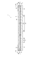
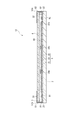
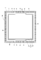
- FIG. 2 is a longitudinal sectional view taken along line II-II in FIG.
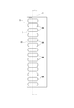
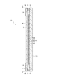
- FIG. 3 is a cross-sectional plan view taken along line III-III in FIG. 2.
- the longitudinal cross-sectional view which shows the example of the photoelectric conversion apparatus which formed the insulating film on the board
- the perspective view which shows the photoelectric conversion apparatus which concerns on 8th embodiment of this invention.
- the plane sectional view showing an example of the photoelectric conversion device concerning a ninth embodiment of the present invention.
- the plane sectional view showing another example of the photoelectric conversion device concerning a ninth embodiment of the present invention.
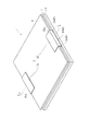
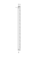
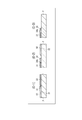
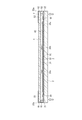
- FIG. 1 is a perspective view showing the entire photoelectric conversion apparatus according to the present embodiment.
- FIG. 2 is a longitudinal sectional view taken along the line II-II in FIG.
- FIG. 3 is a cross-sectional plan view taken along line III-III in FIG.
- the photoelectric conversion device 1 includes a substrate 2, a photoelectric conversion element 3 provided on the substrate 2, a sealing member 4 disposed above the substrate 2 and facing the substrate 2, and the sealing member 4.
- the extraction electrode 5 provided on the surface opposite to the surface facing the photoelectric conversion element 3, the side surface conductive portion 6 electrically connected to the extraction electrode 5, and provided outside the photoelectric conversion element 3
- An adhesive member 7 that bonds the substrate 2 and the sealing member 4, a substrate conductive portion 9 that is electrically connected to the photoelectric conversion element 3 and extends to the outside of the adhesive member 7, and an end of the substrate 2 rather than the adhesive member 7
- an electrical connection member 8 that electrically connects the side conductive part 6 and the board conductive part 9 on the part side.
- FIG. 2 is also a cross-sectional view of the photoelectric conversion device 1 in the thickness direction when the sealing member 4 is viewed with respect to the substrate 2, and FIG. 3 shows a direction along the surface of the substrate 2. It is also a plan sectional view when the cross section of the photoelectric conversion device 1 is viewed toward the substrate 2.
- 2 and 3 are also diagrams for explaining a structure for electrically connecting a photoelectric conversion element (organic EL element) 3 and an extraction electrode 5 described later.
- the substrate 2 is a smooth plate-like member for supporting the organic EL element 3 (photoelectric conversion element 3).
- the light-transmitting substrate 2 is used, and the light transmittance in the visible region of 400 to 700 nm is preferably 50% or more.
- a glass plate, a polymer plate, etc. are mentioned. Examples of the glass plate include soda lime glass, barium / strontium-containing glass, lead glass, aluminosilicate glass, borosilicate glass, barium borosilicate glass, and quartz.
- the substrate 2 is a translucent substrate, and the substrate 2 side is the light extraction direction of the organic EL element 3.
- an opaque substrate such as a silicon substrate or a metal substrate can be used in addition to the light-transmitting substrate 2.
- the portion of the substrate 2 that performs electrical extraction from the anode 31 of the organic EL element 3 is defined as a connection portion 21, and the portion that performs electrical extraction from the cathode 32 of the organic EL element 3 is connected. Part 22 is assumed.
- the substrate 2 when a plurality of photoelectric conversion devices 1 are arranged adjacent to each other, for example, a plate material having a vertical length of about 100 mm, a horizontal length of about 100 mm, and a thickness of about 0.7 mm is used. be able to.
- substrate 2 may cut out and use the board
- the organic EL element 3 includes an anode 31 as a first electrode 31 formed on the substrate 2, a cathode 32 as a second electrode 32 formed at a position facing the anode 31,
- the organic compound layer 33 is disposed between the anode 31 and the cathode 32. That is, the organic EL element 3 is configured such that the anode 31, the organic compound layer 33, and the cathode 32 are stacked in this order from the substrate 2 side.
- the organic EL element 3 may be configured with the first electrode 31 as a cathode and the second electrode 32 as an anode.
- the organic compound layer 33 may be composed of, for example, a single light emitting layer, or may be composed of various anode layers interposed between the anode 31 and the cathode 32 and the light emitting layer.
- the intermediate layer include a hole injection layer, a hole transport layer, an electron injection layer, and an electron transport layer.
- the organic compound layer 33 referred to in this embodiment refers to a layer including at least one layer composed of an organic compound.
- a known light emitting material such as Alq 3 is used for the light emitting layer, which has a structure showing monochromatic light such as red, green, blue, yellow, etc., or a light emitting color by a combination thereof, for example, a structure showing white light emission Etc. are used.
- a doping method is known in which a host is doped with a light emitting material as a dopant. In the light emitting layer formed by the doping method, excitons can be efficiently generated from the charge injected into the host. And the exciton energy of the produced
- a known electrode material is used, and when the light extraction direction is the substrate 2 side, for example, ITO (indium tin oxide), IZO (registered trademark) (indium zinc oxide), ZnO ( A transparent electrode material such as zinc oxide) is used.
- ITO indium tin oxide
- IZO registered trademark
- ZnO A transparent electrode material such as zinc oxide
- a known electrode material is used for the cathode 32, and when the light extraction direction is the substrate 2 side, a metal or an alloy can be used, for example, Ag or Al.
- a metal, an alloy, or the like is used for the anode 31, and a transparent electrode material is used for the cathode 32.
- auxiliary electrodes 34 (34a, 34b, 34c) are formed on the substrate 2 as shown in FIG.
- the auxiliary electrode 34 is provided so that a voltage drop due to the electrical resistance of the transparent electrode material used for the anode 31 is prevented, the voltage is uniformly supplied to the entire anode 31, and the organic EL element 3 emits light uniformly.
- the auxiliary electrode 34 is formed in a linear shape so as to be sandwiched between the substrate 2 and the anode 31.
- the auxiliary electrodes 34 are formed so as to extend in the vertical direction with respect to the paper surface of FIG. 2, and the auxiliary electrodes 34 are electrically connected to each other at a position not shown.
- a known electrode material is used for the auxiliary electrode 34, and a metal or an alloy can be used. For example, Cu, Ag, Al, or the like is used.
- the substrate conductive portion 9 includes a first substrate conductive portion 91 electrically connected to the anode 31 of the organic EL element 3 and a second substrate conductive portion 92 electrically connected to the cathode 32. Are provided on the substrate 2.
- the first substrate conductive portion 91 is connected to the end of the anode 31 and extends from the connection position to the end of the substrate 2 on the connection portion 21 side (left side in FIG. 2). 7 and an electrical connection member 8 (an electrical connection member 81 described later). More specifically, it passes between the adhesive member 7 and the electrical connection member 8 and the substrate 2.
- the second substrate conductive portion 92 is connected to the end portion of the cathode 32 and extends from the connection position to the end portion on the connection portion 22 side of the substrate 2 (the right side in FIG. 2). 7 and the electric connection member 8 (electric connection member 82 described later). More specifically, it passes between the adhesive member 7 and the electrical connection member 8 and the substrate 2.
- a known electrode material is used for the substrate conductive portion 9, and a metal or an alloy can be used. For example, Cu, Ag, Al, or the like is used. Note that the same material as the anode 31 and the cathode 32 can be used.
- the substrate conductive portion 9 has a width of about one-fourth to one-third of the length of one side when the substrate 2 is viewed in plan (connection with the anode 31 and the cathode 32). In a direction substantially orthogonal to the direction).
- the width of the substrate conductive portion is designed according to the amount of current required for the element.
- the substrate conductive portion 9 is connected to the auxiliary electrode 34 (not shown). For this reason, the present invention is not limited to display applications in which electrodes are arranged in a matrix, and even when a large amount of current is required to drive an organic EL element 3 for illumination, for example, in which electrodes are arranged in a plane, stable electrical Connection can be secured.
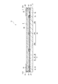
- FIG. 4 is a diagram when the substrate conductive portion 9 is viewed in plan, and only the substrate conductive portion 91 in FIG. 3 is taken out and illustrated. Therefore, the left long side of the substrate conductive portion 91 formed in a substantially rectangular shape in plan view is actually along the end portion of the substrate 2. Then, as shown in FIG. 4, a plurality of holes 9 ⁇ / b> A are formed side by side along the left long side of the substrate conductive portion 9. Further, the positions where the plurality of holes 9A are formed correspond to positions where an adhesive member 7 and an electrical connection member 8, which will be described later, shown by a two-dot chain line in FIG. 4 are provided, and the adhesive member 7 and the electrical connection member 8 are provided. It is formed so as to straddle.
- the substrate conductive portion 91 is illustrated and described, and the substrate conductive portion 92 is not illustrated, but the substrate conductive portion 92 is similarly formed with holes.
- Examples of the method for forming the holes 9A include mask sputtering.
- the hole 9 ⁇ / b> A is necessary when the adhesive member 7 and the electrical connection member 8 are heated and melted by laser irradiation to achieve bonding and electrical connection in the manufacturing process of the photoelectric conversion device 1. If the hole 9A is not formed in the substrate conductive portion 9, even if the laser is irradiated from the substrate 2 side, the heat from the laser irradiation is absorbed by the substrate conductive portion 9, and the adhesive member 7 and the electrical connection member 8 are heated. There is a risk that it will not melt.
- the hole 9A is formed, the laser passes through the hole 9A and reaches the adhesive member 7 and the electrical connection member 8. Therefore, the adhesive member 7 and the electrical connection member 8 are smoothly heated by the laser. And can be melted and joined and electrically connected. In particular, when the adhesive member 7 is melted and joined to the substrate 2, the sealing performance is improved. Note that the hole 9A is not shown in the substrate conductive portion 9 in other figures.
- An internal insulating film as an insulating film may be formed on the substrate conductive portion 9.
- the internal insulating film can prevent a short circuit between the cathode 32 and the substrate conductive portion 91 even when the cathode 32 is formed on the substrate conductive portion 91.
- an internal insulating film may be formed on the auxiliary electrode 34.
- the internal insulating film is formed on the auxiliary electrode 34 adjacent to the end portion of the anode 31, and is preferably formed on the auxiliary electrode 34c shown in FIG. If the internal insulating film is formed, a short circuit between the cathode 32 and the auxiliary electrode 34c can be prevented.
- the range for forming the internal insulating film is not limited to cover the whole of the substrate conductive portion 9 and the auxiliary electrode 34, but may be formed in a range that can prevent a short circuit.
- the substrate conductive portion 9 and the auxiliary electrode 34 may be formed. It may be formed on a part of the top.
- the internal insulating film may be made of an electrically insulating material.
- the internal insulating film can be formed using silicon oxide (SiO 2 ), aluminum oxide, or the like by mask vapor deposition or mask sputtering.
- the internal insulating film is preferably formed after the anode 31 is formed.
- the internal insulating film may be formed at a position where the short circuit between the anode 31 and the cathode 32 and the substrate conductive portion 9 and the auxiliary electrode 34 can be prevented, and a position where the electrical connection member 8 is not covered. That's fine.
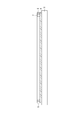
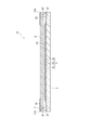
- FIG. 5 is a cross-sectional view of the photoelectric conversion device 11 in which the internal insulating film 35 is formed on the substrate conductive portion 91 and the auxiliary electrode 34 c when viewed in the thickness direction with respect to the substrate 2 with the sealing member 4 facing upward. It is.
- the configuration of the photoelectric conversion device 11 has substantially the same configuration as that of the photoelectric conversion device 1, but the shape of the inner insulating film 35 and the shapes of the end portions of the anode 31, the cathode 32, and the organic compound layer 33 are the same. Different from the photoelectric conversion device 1.
- the cathode 32 extends further to the connection portion 21 side (left side in FIG.
- the internal insulating film 35 is formed on the substrate conductive portion 91, the internal insulating film 35 is interposed between the substrate conductive portion 91 and the cathode 32, and the electrical connection between the cathode 32 and the substrate conductive portion 91 is performed. Connection is prevented.
- the cathode 32 extends to the connection portion 22 side (the right side in FIG. 5) of the substrate 2, rides over the auxiliary electrode 34 c, and rides on the substrate conductive portion 92.
- the organic compound layer 33 is formed over the auxiliary electrode 34c, and the organic compound layer 33 is interposed between the auxiliary electrode 34c and the cathode 32.
- the organic compound layer 33 does not extend over the auxiliary electrode 34c, the cathode 32 and the auxiliary electrode 34c are electrically connected, and the cathode 32 and the anode 31 may be short-circuited. is there.
- the internal insulating film 35 is formed on the auxiliary electrode 34c, the internal insulating film 35 is interposed between the auxiliary electrode 34c and the cathode 32, and the electrical connection between the cathode 32 and the substrate conductive portion 92 is achieved. Connection is prevented.
- the anode 31 extends to the substrate conductive portion 92 and is electrically connected, if the internal insulating film 35 is formed on the substrate conductive portion 92, the anode 31 and the cathode are formed as described above. The short circuit with 32 can be prevented.
- the sealing member 4 is one of the members for sealing the organic EL element 3, and is a member that is disposed on the upper side of the organic EL element 3 so as to face the substrate 2 as shown in FIG.
- the organic EL element 3 is sealed as follows. First, the substrate 2 is disposed below the organic EL element 3, and the sealing member 4 is disposed above the organic EL element 3. When the photoelectric conversion device 1 is viewed in cross-section in the substrate thickness direction as shown in FIG. 2, the photoelectric conversion device 1 is disposed outside the organic compound layer 33 of the organic EL element 3 as shown in FIG.
- the adhesive member 7 is provided so as to surround the periphery of the organic compound layer 33 in a frame shape when viewed in cross-section in the direction along the surface 2.
- the sealing member 4 is preferably a plate-like, film-like, or foil-like member. Specifically, a glass plate, a polymer plate, a film, a metal plate, a metal foil, etc. are mentioned.
- the plate-shaped member is used for the sealing member 4 in this embodiment, for example, a cap-shaped object or a plate-shaped object (for example, a seat) having a recess having an inner dimension larger than the outer dimension of the organic EL element 3 is used. (Grid substrate), sheet-like material or film-like material.
- the sealing member 4 is preferably formed to be the same as the substrate 2 or smaller than the substrate 2.
- the sealing member 4 is bonded to the substrate 2 when the photoelectric conversion device 1 is viewed in plan view.
- the thickness of the side conductive portion 6 is preferably the same as the thickness of the side conductive portion 6 relative to the end of 2, or offset so as to be slightly inside.
- the offset dimension may not be the entire sealing member 4, and corresponds to the connection portion 21 and the connection portion 22 of the substrate 2 when the substrate 2 and the sealing member 4 are joined. Only a part may be sufficient.
- the thickness dimension of the sealing member 4 is preferably 0.1 mm or more and 5 mm or less. If the thickness dimension is 0.1 mm or less, the air permeability increases and the sealing performance decreases.
- the extraction electrode 5 is an electrode for electrically extracting the electrodes 31 and 32 of the photoelectric conversion element 3 sealed inside the photoelectric conversion device 1 to the outer surface side of the photoelectric conversion device 1.
- the sealing member 4 is provided on the surface opposite to the surface facing the organic EL element 3.
- the extraction electrode 5 is a part for connecting wiring from an external power source for applying a voltage to the anode 31 and the cathode 32.
- the extraction electrode 5 is a portion for connecting a wiring to an external device in order to extract the electric charge generated by the solar cell element to the outside. As shown in FIGS.
- the extraction electrode 5 is a pair of electrodes of a first extraction electrode 51 and a second extraction electrode 52 on the surface opposite to the surface facing the organic EL element 3 of the sealing member 4. It is provided as. And the 1st extraction electrode 51 and the 2nd extraction electrode 52 have protrusion part 51a, 52a which protrudes outside from the edge part of the sealing member 4, respectively.
- the first extraction electrode 51 and the second extraction electrode 52 are electrically connected to the anode 31 and the cathode 32 via the side surface conductive portion 6, the electrical connection member 8, and the substrate conductive portion 9, respectively. ing.
- the positions and shapes of the first extraction electrode 51 and the second extraction electrode 52 are formed so as to correspond to the connection portions 21 and 22 of the substrate 2 as shown in FIGS.
- the sealing member 4 is formed to be smaller than the substrate 2 by a predetermined dimension, and the protruding portions 51a and 52a are substantially flush with the side surface of the substrate 2 as shown in FIG. Is provided.
- the side surface conductive portion 6 is a portion that is disposed on the side surface of the photoelectric conversion device and ensures electrical connection between the extraction electrode 5 and the organic EL element 3.
- the side conductive portion 6 is provided outside the end portion of the sealing member 4 and is electrically connected to the extraction electrode 5.
- the side surface conductive portion 6 includes side surface conductive portions 61 and 62 that are electrically connected to the protruding portions 51a and 52a in the vertical direction.
- the side surface conductive portion 6 is formed integrally with the extraction electrode 5, and the side surface conductive portion 6 is formed so as to cover the end surface of the sealing member 4. And the front-end
- the sealing member 4 is formed to be smaller than the substrate 2 by a predetermined dimension, and the side surface conductive portions 61 and 62 are substantially flush with the side surface of the substrate 2 as shown in FIG. It is provided as follows. By doing in this way, when arrange
- the adhesive member 7 is one of the members for sealing the organic EL element 3 and joins the substrate 2 and the sealing member 4. And the adhesive member 7 can seal an organic compound layer by forming in the frame shape around the organic compound layer 33, as shown in FIG. As shown in FIG. 2, in the portion where the substrate conductive portion 9 is formed, the adhesive member 7 joins the substrate 2 and the sealing member 4 across the substrate conductive portion 9.
- the position (bonding position) where the adhesive member 7 is provided depends on the size of the substrate 2 and the space where the electrical connection member 8 is provided, but in order to widen the area where the organic EL element 3 can be set, The side is preferred.
- the distance from the end of the substrate 2 to the adhesive member 7 is 0.1 mm or more and 0. .3 mm or less is particularly preferable.
- the adhesive member 7 is preferably made of an inorganic compound from the viewpoints of sealing properties, moisture resistance, and bonding strength.
- Low melting glass is preferred because it can be formed by laser irradiation.
- the low melting point in the present invention means that having a melting point of 650 ° C. or lower.
- the melting point is preferably 300 ° C. or higher and 600 ° C. or lower.
- the low-melting glass preferably includes a transition metal oxide capable of bonding glass and metal, a rare earth oxide, and the like, and more preferably powder glass (frit glass).
- powder glass powder glass
- the substrate 2 and the sealing member 4 cover the upper and lower sides of the organic EL element 3, the adhesive member 7 surrounds the periphery of the organic EL element 3, and the substrate 2 and the sealing member 4 are joined. By doing so, the organic EL element 3 is sealed. At this time, a space surrounded by the substrate 2, the sealing member 4, and the adhesive member 7 is a sealing space S. In addition to the organic EL element 3 being provided in the sealed space S, the heat dissipation member 43 is filled.
- the heat radiating member 43 plays a role of efficiently transmitting heat generated in the organic EL element 3 to the sealing member 4 side.
- an inactive member having good thermal conductivity is preferable, and for example, fluorine oil can be used.
- the electrical connection member 8 is one of members for electrically connecting the side surface conductive portion 6 and the substrate conductive portion 9 to ensure electrical connection from the extraction electrode 5 to the organic EL element 3. As shown in FIGS. 2 and 3, the electrical connection member 8 is provided on the outer side (the end portion side of the substrate 2) than the adhesive member 7. An electrical connection member 81 is connected to the side conductive part 61 and the board conductive part 91, and an electrical connection member 82 is connected to the side conductive part 62 and the board conductive part 92. As shown in FIG. 2, each of the electrical connection members 81 and 82 has the electrical connection member 8 in a space between the adhesive member 7 and the side surface conductive portions 61 and 62. Further, as shown in FIG.
- the electrical connection members 81 and 82 are electrically connected to the substrate conductive portions 91 and 92 in the vertical direction, respectively, and the substrate is connected to the inside of the side surface conductive portions 61 and 62, respectively. Electrical connection is made in the direction along the surface of 2. Further, as shown in FIG. 3, the electrical connection members 81 and 82 are provided with substantially the same width as the widths of the substrate conductive portions 91 and 92. Therefore, a wide electrical continuity can be obtained, so that a stable electrical connection can be ensured.
- a conductive adhesive or a solder material can be used as the electrical connection member 8.
- a low melting point solder material having a melting point of 300 ° C. or lower is preferable.
- FIG. 6A is a schematic view showing the manufacturing process on the sealing member 4 side.
- 6A to 6C are views showing a cross section in the thickness direction of the sealing member 4, and show a case where an adhesive member 7 or the like is applied on the sealing member 4.
- FIG. 6A the adhesive member 7 is applied on one surface of the sealing member 4.
- frit glass is used as the adhesive member 7.
- the application position of the adhesive member 7 is the end side of the sealing member 4, and when bonded to the substrate 2, the bonding position surrounds the organic compound layer 33 in a frame shape as shown in FIG.
- variety of the adhesive member 7 may become a joining width which can ensure joining strength.
- the application method include a dispenser method.
- the electrical connection member 8 is applied to the end side of the sealing member 4 with respect to the adhesive member 7.
- a low melting point solder material is used as the electrical connection member 8.
- the application position of the electrical connection member 8 is a position corresponding to a site where electrical connection with the substrate conductive portion 9 is performed. Examples of the application method include a dispenser method.
- the adhesive member 7 and the electrical connection member 8 used here are pasty at the time of application, and each contains an alcohol component.
- a heating means H such as a hot plate is disposed on the surface opposite to the surface of the sealing member 4 to which the adhesive member 7 and the electrical connection member 8 are applied.
- the sealing member 4 is heated from the surface and fired. By this baking, the above-mentioned alcohol component contained in the adhesive member 7 and the electrical connection member 8 is removed.
- a heating method it is good also as a method of putting the said sealing member 4 in a heating furnace.
- a heat radiation member 43 is applied on the surface of the sealing member 4 to which the adhesive member 7 and the electrical connection member 8 are applied. Examples of the application method include a dispenser method.
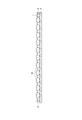
- FIG. 7A to 7D are schematic diagrams for explaining a manufacturing process on the substrate 2 side in the photoelectric conversion device 1.
- FIG. 7A to 7D are views showing a cross section in the thickness direction of the substrate 2, and show a case where the organic EL element 3 is formed on the substrate 2.
- FIG. 7A to FIG. 7D alphabets and numbers are given according to the parts of the substrate 2. The alphabet indicates each manufacturing process on the substrate 2 side, the numeral 1 indicates that the periphery of the connection portion 21 on the left side of FIG. 2 is indicated, and 2 indicates that the periphery of the connection portion 22 on the right side of FIG. Represents a peripheral portion of the substrate 2 other than the connection portions 21 and 22.
- auxiliary electrodes 34a, 34b, 34c (only the auxiliary electrode 34c is shown in the figure) and substrate conductive portions 91, 92 are formed on the substrate 2.
- the substrate conductive portions 91 and 92 are formed by a mask sputtering method or the like so that the above-described hole 9A (see FIG. 4) is formed.
- the anode 31 is formed on the substrate 2.
- a known method such as vacuum deposition or sputtering can be employed.
- auxiliary electrode 34c is in contact with the anode 31 on the side surface.
- the outer edge of the anode 31 is formed to extend to the substrate conductive portion 91, and in FIG. 7B (B-2) and (B-3). As shown, it is formed in a region inside the substrate 2 with respect to the auxiliary electrode 34c.
- the organic compound layer 33 is formed on the anode 31.
- a forming method a known method such as a dry film forming method such as vacuum deposition, sputtering, plasma, or ion plating, or a wet film forming method such as spin coating, dipping, flow coating, or ink jet can be employed.
- a masking means it is preferable to perform layer formation by applying a masking means so that the organic compound layer 33 is formed at a predetermined position. As shown in (C-2) of FIG.
- the end of the organic compound layer 33 on the substrate conductive portion 92 side passes over the auxiliary electrode 34c, and the substrate 2 between the auxiliary electrode 34c and the substrate conductive portion 92 is placed. It extends to the part where the surface is exposed.
- the end portion of the organic compound layer 33 on the substrate conductive portion 91 side is offset to a region inside the end portion of the anode 31 on the substrate conductive portion 91 side. Is formed.
- the cathode 32 is formed on the organic compound layer 33.
- a known method such as vacuum deposition or sputtering can be employed.
- mask sputtering or the like is preferably performed so that the cathode 32 is formed at a predetermined position.
- the end of the cathode 32 on the substrate conductive portion 92 side is formed so as to extend over the auxiliary electrode 34c and further onto the substrate conductive portion 92.
- the end portion of the cathode 32 on the substrate conductive portion 91 side is less than the end portion of the organic compound layer 33 on the substrate conductive portion 91 side so as not to be short-circuited. It is offset and formed inside.
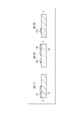
- FIGS. 8A to 8C are schematic views for explaining a process of bonding the sealing member 4 side and the substrate 2 side manufactured in the above process.
- FIGS. 8A to 8C are views of the cross section in the thickness direction of the substrate 2 and the sealing member 4, and show the case where the substrate 2 and the sealing member 4 are bonded in the vertical direction.
- the surface of the sealing member 4 on which the adhesive member 7 and the electrical connection member 8 are applied is directed upward, and the surface of the substrate 2 on which the organic EL element 3 is formed is directed downward.
- FIG. 8B the sealing member 4 is pressed in the direction of the arrow, and the heat dissipating member 43 applied on the sealing member 4 is stretched and filled in the sealing space S.
- the first extraction electrode 51 and the second extraction electrode 52 are formed on the sealing member 4 with the sealing member 4 facing upward.
- the metal foil is processed and formed in advance by press molding so that the side conductive parts 61 and 62 are formed, and the metal foil is fixed to the sealing member 4 with an epoxy resin. The side conductive parts 61 and 62 are brought into contact with the electrical connection member 8.
- the bonded portion is locally heated by laser irradiation or the like in the arrow direction while maintaining the contacted state, and the adhesive member 7 and the electrical connection member 8 are melted and heated.
- the adhesive member 7 and the electrical connection member 8 are bonded to members that are in contact with them.
- the laser output and the laser moving speed are adjusted so that the temperature of the adhesive member 7 becomes 600 ° C.
- the adhesive member 7 made of frit glass surrounds the outside of the organic compound layer 33 of the organic EL element 3 in a frame shape, and the substrate 2 and the sealing member 4 are bonded.
- the photoelectric conversion device 1 having a narrow frame structure having high bonding strength and excellent sealing performance can be obtained.
- An electrical connection member 8 is provided at a position further outside the adhesive member 7, and the electrical connection member 8 is electrically connected to the inner side of the side surface conductive portion 6, and is vertically connected to the substrate conductive portion 9. Since electrical connection is made in the direction, stable electrical connection can be ensured. Moreover, by providing the electrical connection member 8 inside the side surface conductive portion 6, blurring of the electrical connection member 8 before laser processing is suppressed, and the manufacturing yield of the photoelectric conversion device 1 is improved.
- the organic EL element 3 is electrically connected to the extraction electrode 5 through the substrate conductive portion 9, the electrical connection member 8, and the side surface conductive portion 6, and the extraction electrode 5 is in the thickness direction of the substrate 2. Therefore, the gap between the photoelectric conversion devices 1 can be narrowed and the joint between the devices becomes inconspicuous.
- the electrical connection member 8 Since the electrical connection member 8 is provided in the space between the adhesive member 7 and the side surface conductive portion 6, the electrical connection member 8 on the end portion side of the substrate 2 is well accommodated in the photoelectric conversion device 1.
- the electric connection member 8 does not protrude outside the side surface conductive portion 6. Therefore, even when a plurality of photoelectric conversion devices 1 are arranged adjacent to each other, the electrical connection members 8 that protrude from the end side of the substrate 2 do not interfere with each other, and also from this point, the intervals between the photoelectric conversion devices 1 are reduced. And the joint between the photoelectric conversion devices 1 becomes inconspicuous.
- first extraction electrode 51 and the side surface conductive portion 61 are configured by one member, and the second extraction electrode 52 and the side surface conductive portion 62 are configured by one member, electrical extraction from the organic EL element 3 is performed.
- the number of members necessary for the process can be reduced, and the structure and manufacturing process of the photoelectric conversion device 1 can be simplified.
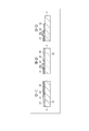
- FIG. 9 is a cross-sectional view of a cross section in the thickness direction of the photoelectric conversion device 12 according to the second embodiment.
- the photoelectric conversion device 12 according to the second embodiment differs from the photoelectric conversion device 1 according to the first embodiment in the method of joining the side surface conductive portion 6 and the electrical connection member 8. That is, the side surface conductive portions 61 and 62 protrude to positions where they face the substrate conductive portions 91 and 92 on the end side of the substrate 2, respectively, and the tips (lower ends in FIG.
- the electrical connection member 8 is not provided in a space formed between the outside of the adhesive member 7 and the inside of the side surface conductive portion 6, and as shown in FIG. In addition, an electrical connection is made in the vertical direction with respect to the side surface conductive portion 6. Therefore, the joining position by the adhesive member 7 is further provided on the end side of the substrate 2 as compared with the case of the first embodiment.
- the same effects as (1) to (3) and (5) to (7) in the first embodiment are exhibited, and the following effects are also achieved.
- (8) The space for providing the electrical connection member 8 formed between the outside of the adhesive member 7 and the inside of the side surface conductive portion 6 is reduced, and the adhesive member 7 is further provided on the outer side (end side of the substrate 2). I can do it. Therefore, the space on the substrate 2 for arranging the organic EL element 3 can be further widened while ensuring the reliability of conduction between the side surface conductive portion 6 and the substrate conductive portion 9, resulting in a larger light emitting area. I can do it.
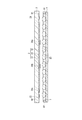
- FIG. 10 is a cross-sectional view of a cross section in the thickness direction of the photoelectric conversion device 13 according to the third embodiment.
- the photoelectric conversion device 13 according to the third embodiment is different from the photoelectric conversion device 1 according to the first embodiment in the structure of the extraction electrode 5 and the side surface conductive portion 6. That is, the extraction electrode 5 and the side conductive portion 6 are configured separately.
- the same material as that described in the first embodiment can be used as the material that can be used for the extraction electrode 5 and the side surface conductive portion 6.
- the extraction electrode 5 and the side surface conductive part 6 may be comprised with the same member, and may be comprised with a different member. Examples of a method for connecting the extraction electrode 5 and the side conductive portion 6 include solder connection, fusion, and welding.
- the members constituting the first extraction electrode 51 and the second extraction electrode 52 are bent at the end side of the sealing member 4 to form the side conductive portions 61 and 62. Since it is difficult to perform the processing, it is easy to manufacture the photoelectric conversion device in which the sealing member is thin by configuring the side surface conductive portions 61 and 62 as separate members.
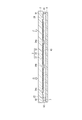
- FIG. 11 is a cross-sectional view of a cross section in the thickness direction of the photoelectric conversion device 14 according to the fourth embodiment.
- the photoelectric conversion device 14 according to the fourth embodiment is different from the photoelectric conversion device 13 in the electrical connection structure of the electrical connection member 8 in the photoelectric conversion device 13 according to the third embodiment.
- the side conductive parts 61 and 62 are electrically connected in the vertical direction to the protruding parts 51a and 52a of the extraction electrodes 51 and 52, respectively, and are electrically connected in the vertical direction to the substrate conductive parts 91 and 92, respectively.
- the side conductive parts 61 and 62 may be formed of the same member as the electrical connection member 8 described above.
- the adhesive member 7 is further provided in comparison with the first embodiment and the third embodiment. It can be provided on the outside (the end side of the substrate 2). Therefore, the space on the substrate 2 for disposing the organic EL element 3 can be further increased, and as a result, the light emitting area and the like can be further increased.
- the side conductive parts 61 and 62 are formed by bending the members constituting the first extraction electrode 51 and the second extraction electrode 52 on the end side of the sealing member 4.
- this connection structure in which the first extraction electrode 51 and the second extraction electrode 52 are directly connected to the extraction electrode by the side conductive parts 61 and 62 separate from each other is necessarily effective.
- a low melting point metal is used for the side conductive parts 61 and 62, for example, if the sealing member 4 has a thickness of about 1 mm, the low melting point metal can be easily disposed on the side conductive parts 61 and 62. And electrical continuity can be ensured.
- FIG. 12 is a cross-sectional view of a cross section in the thickness direction of the photoelectric conversion device 15 according to the fifth embodiment.
- the photoelectric conversion device 15 according to the fifth embodiment is different from the photoelectric conversion device 13 according to the third embodiment in that the anode 31 and the cathode 32 of the organic EL element 3 are extended to the end side of the substrate 2. Different from the converter 13.
- FIG. 13 is a cross-sectional view of a cross section in the thickness direction of the photoelectric conversion device 16 according to the sixth embodiment.
- the photoelectric conversion device 16 according to the sixth embodiment is different from the photoelectric conversion device 14 according to the fourth embodiment in that the anode 31 and the cathode 32 of the organic EL element 3 are extended to the end side of the substrate 2. Different from the photoelectric conversion device 14.
- FIG. 14 is a cross-sectional view of a cross section in the thickness direction of the photoelectric conversion device 17 according to the seventh embodiment.
- the photoelectric conversion device 17 according to the seventh embodiment is such that the sealing member 4 is a conductive sealing member 41 in the photoelectric conversion device 1 according to the first embodiment.
- the second extraction electrode 52, the side conductive portion 62, and the portion where the electrical connection member 82 and the conductive sealing member 41 are in contact with each other are externally insulated as an insulating portion so as not to contact each other and to be short-circuited.
- a layer 42 is provided. As shown in FIG. 14, the outer insulating layer 42 extends from the upper surface of the conductive sealing member 41 to the lower surface through the side surface.
- the anode 31 of the organic EL element 3 is electrically connected to the first extraction electrode 51 via the substrate conductive portion 91, the electrical connection member 81, and the side surface conductive portion 61, and the first extraction electrode 51 is electrically conductive.
- the sealing member 41 is connected.
- the connection between the first extraction electrode 51 and the conductive sealing member 41 only needs to be connected in a state where conduction is ensured.
- the conductive sealing member 41 may be any member having conductivity, and for example, a metal plate or foil can be used. Moreover, as long as the surface of the sealing member 4 is covered with a conductive material, the sealing member 4 itself may not be conductive.
- the outer insulating layer 42 may be formed of an electrically insulating material.
- the external insulating layer 42 can be formed of silicon oxide (SiO 2 ), aluminum oxide, or the like by a mask vapor deposition method, a mask sputtering method, or the like. Alternatively, an insulating film, a foil, or the like can be attached to the conductive sealing member 41 and formed.
- the sealing member 4 in the photoelectric conversion device 17 is the conductive sealing member 41, and the anode 31 of the organic EL element 3 is electrically connected to the first extraction electrode 51 through the electrical connection member 8 and the like. Further, it is electrically connected to the conductive sealing member 41. Therefore, the wiring from the external power supply on the anode 31 side can be connected not only to the first extraction electrode 51 but also to the conductive sealing member 41, and flexibility in the electrical connection position occurs.
- FIG. 15 is a perspective view showing the photoelectric conversion device 18 provided with a plurality of first extraction electrodes 51 and second extraction electrodes 52.
- the photoelectric conversion device 18 according to the eighth embodiment is the same as the photoelectric conversion device 1 according to the first embodiment in that two first extraction electrodes 51 and two second extraction electrodes 52 are provided. Different from 1.
- the present invention not only the pair of the first extraction electrode 51 and the second extraction electrode 52 is provided, but also the first extraction electrode 51 and the second extraction electrode as in the above-described embodiment.
- a plurality of at least one of 52 may be provided. Since the extraction electrode 5 reduces the sheet resistance of the first electrode or the second electrode, it is preferable to provide a plurality of extraction electrodes 5 because the sheet resistance can be further reduced. Of the first electrode or the second electrode, it is preferable to provide more extraction electrodes that are electrically connected to the one using a transparent electrode such as ITO having a high sheet resistance, or a larger electrode area.
- the anode as the first electrode is a transparent electrode made of ITO
- the cathode as the second electrode is an electrode made of aluminum.
- the area of the first extraction electrode 51 connected to the anode is made larger than that of the second extraction electrode 52 in order to reduce the sheet resistance of the anode (FIG. 15). reference). From the viewpoint of preventing light emission unevenness, it is effective to increase the number of first extraction electrodes 51 compared to the number of second extraction electrodes 52 in order to suppress a voltage drop due to ITO having a high sheet resistance.
- FIG. 16 is a plan cross-sectional view of a cross section of the photoelectric conversion device 19 ⁇ / b> A in a direction along the surface of the substrate 2 as viewed toward the substrate 2.
- FIG. 17 is a plan cross-sectional view of a cross section of the photoelectric conversion device 19 ⁇ / b> B in the direction along the surface of the substrate 2 as viewed toward the substrate 2.
- the photoelectric conversion devices 19 ⁇ / b> A and 19 ⁇ / b> B according to the ninth embodiment are different from the photoelectric conversion device 1 in that the light reflection unit 36 is provided on the substrate 2 in the photoelectric conversion device 1 according to the first embodiment.
- 16 and 17 is substantially the same as the position of FIG. 3 according to the first embodiment.
- the side conductive parts 61 and 62, the adhesive member 7, and the electrical connection members 81 and 82 are indicated by two-dot chain lines for convenience of explanation.
- the light reflecting portion 36 is a layer that is made of a material that reflects light and reflects light generated in the organic compound layer 33 in the light extraction direction.
- the light reflecting portion 36 is formed, for example, by forming a metal film by vapor deposition or attaching a metal foil or a metal plate.
- substrate conductive part 9 is comprised with metals, such as Al, Cu, Ag, it is preferable to form the light reflection part 36 with the same member as the said board
- the light reflecting portion 36 is provided at a position different from the position where the substrate conductive portion 9, the auxiliary electrode 34, and the organic EL element 3 are formed on the substrate 2. Further, it is preferably provided over the entire position different from the position where the substrate conductive portion 9, the auxiliary electrode 34, and the organic EL element 3 are formed. Therefore, any one of the substrate conductive portion 91, the substrate conductive portion 92, and the auxiliary electrode may be formed integrally with the light reflecting portion 36 so that the area of the light reflecting portion 36 is as large as possible.
- the light reflecting portion 36 is composed of a conductive member
- the anode 31 of the organic EL element 3 and Since the cathode 32 may be short-circuited a short-circuit is caused by providing a predetermined dimensional gap between the light reflecting portion 36 and one of the substrate conductive portion 91 and the substrate conductive portion 92 or by interposing an insulating material. It is preferable to prevent.
- a plurality of holes 9 ⁇ / b> A are formed along the edge of the substrate 2 in the substrate conductive portion 9 and the light reflecting portion 36 of the photoelectric conversion device 19 ⁇ / b> A. That is, the hole 9 ⁇ / b> A of the substrate conductive portion 9 described in the first embodiment is also formed in the light reflecting portion 36.
- the substrate conductive portion 9 and the light reflecting portion 36 are formed simultaneously.
- the substrate conductive portion 9 and the light reflecting portion 36 are formed by the sputtering method or the like using the same metal material (Al or the like), and then pattern etching is performed to form the hole 9A.
- the hole 9A is formed in a substantially elliptical shape.
- a plurality of holes 9 ⁇ / b> B having a shape different from the above-described hole 9 ⁇ / b> A are formed in the substrate conductive portion 9 and the light reflecting portion 36 along the end portion of the substrate 2. .
- the substrate conductive portion 9 and the light reflecting portion 36 are simultaneously formed in the same manner as the photoelectric conversion device 19A.
- the substrate conductive portion 9 and the light reflecting portion 36 are formed in a state having the holes 9B in advance by a mask sputtering method or the like.
- the hole 9 ⁇ / b> B is formed in a substantially rectangular shape and extends inward from the end of the substrate 2.
- the hole 9B is also provided for smooth joining by laser irradiation.
- the same effects as (1) to (7) in the first embodiment are exhibited, and the following effects are also achieved.
- the light emitted from the organic compound layer 33 of the organic EL element 3 is emitted from the substrate 2 as it is in the light extraction direction without propagating through the substrate 2 or is transmitted from the substrate 2 through propagation in the substrate 2.
- the light is emitted in the extraction direction or in the opposite direction.
- the light reflecting portion 36 is provided on the substrate 2 as described above and at a position different from the position where the substrate conductive portion 9 and the like are provided.
- the emitted light that has propagated through the substrate 2 to the provided position is not emitted in the direction opposite to the light extraction direction, but is reflected in the light extraction direction.
- the light reflected in this way is emitted in the light extraction direction, or further propagated toward the end portion of the substrate 2 while being reflected and then emitted in the light extraction direction.
- the light reflection part 36 is formed on the board
- emitted from the organic EL element 3 reaches the junction part in the edge part side of the board
- the said junction part is concealed with light, when the photoelectric conversion devices 19A and 19B are arranged adjacent to each other, the joints and junctions between the photoelectric conversion devices 19A and 19B become less conspicuous.
- the junction can be hidden by light, a structure that improves the junction strength by increasing the junction width of the junction is possible, and the degree of freedom in designing the photoelectric conversion device increases.
- the photoelectric conversion element 3 used in the photoelectric conversion device 1 the organic EL element 3 has been described as an example in the embodiment.
- the photoelectric conversion element 3 is not limited to this, and the organic thin film solar cell element, the dye-sensitized solar cell element, and the like are airtight. Applies to elements that need to be held.
- an organic thin film solar cell element when the substrate 2 side is a light incident surface, a transparent conductive film, a P-type organic semiconductor, an N-type organic semiconductor, and a conductive film are stacked in this order from the substrate 2 side. be able to.
- a transparent electrode member can be used so that light from the substrate 2 side can reach the solar cell layer (P-type organic semiconductor and N-type organic semiconductor).
- P-type organic semiconductor and N-type organic semiconductor For example, ITO (indium tin oxide), ZnO A transparent electrode such as (zinc oxide) or SnO 2 (tin oxide) can be used.
- a metal electrode such as aluminum, gold, silver, or titanium that has low light absorption and high reflection can be used as the reflective film.
- Other configurations can be the same as those in the above embodiment.
- this invention is not limited to the said embodiment,
- transformation shown below is included in the range which can achieve the objective of this invention.
- the sealed space S may be evacuated or filled with a dry gas or the like.
- the external insulating layer 42 may be provided also in a portion where the first extraction electrode 51 and the side surface conductive portion 61 and the conductive sealing member 41 are in contact with each other.
- At least one of the first electrode and the second electrode is connected by the above-described electrical connection structure according to the present invention.
- at least one of the plurality of electrodes is connected by the above-described electrical connection structure according to the present invention. It only has to be done.
- the number, position, area, and the like of the extraction electrode 5 are not limited to the positions described in the above embodiment.
- the first extraction electrode 51 and the second extraction electrode 52 are provided along two opposing sides of the sealing member 4, but the first extraction electrode 51 is provided on each of two adjacent sides of the sealing member 4.
- a second extraction electrode 52 may be provided.
- the 1st extraction electrode 51 and the 2nd extraction electrode 52 are provided in the corner
- a plurality of extraction electrodes 5 are provided, they do not have to have the same area, and can be set as appropriate from the viewpoints of components of the first electrode and the second electrode that are electrically connected.
- a light diffusion layer may be provided on the entire surface of the substrate 2 facing the outside of the photoelectric conversion device or partially. Light emitted from the organic compound layer 33 of the organic EL element 3 can be efficiently extracted outside in the light extraction direction.
- the light diffusion layer is provided by attaching a light diffusion film, vapor deposition, or the like.
- the anode 31 and the cathode 32 are extended to the end portion side of the substrate 2 (see FIG. 12), and after the extension, the anode 31 and the cathode 32 are connected to the substrate end portion side.
- the above-described substrate conductive portion may be further formed between the cathode 32 and the substrate 2.
- the photoelectric conversion device 1 was created based on the configuration of the first embodiment, a drive test was performed, and the evaluation was performed.
- the evaluation items are as follows.
- Device lifetime Evaluate the time to halve the initial luminance. This half time represents the sealing performance in the photoelectric conversion device.
- the driving test was performed under the following conditions. A voltage was applied to the organic EL element 3 so that the current value was 1 mA / cm 2, and the voltage value at that time was measured. Further, the EL emission spectrum at that time was measured with a spectral radiance meter (CS-1000: manufactured by Comica Minolta). From the obtained spectral radiance spectrum, luminance, chromaticity, current efficiency (cd / A), external quantum efficiency (%), and main peak wavelength (nm) were calculated. Further, a continuous DC current test was performed at an initial luminance of 5000 cd / m 2 (nit), and the half life of the device was measured.
- CS-1000 spectral radiance meter
- the structure and member of the photoelectric conversion apparatus used for the drive test are as follows.
- -Substrate Blue plate glass (100 mm x 100 mm, thickness: 0.7 mm)
- Sealing member soda glass (99.95 mm ⁇ 100 mm, thickness: 0.7 mm)
- Extraction electrode Copper foil (thickness 0.08mm)
- Adhesive member frit glass (AGC, AP5346B, melting point 485 ° C.)
- Electrical connection member Solder material (Ishikawa Metals, J3-3230-LU, melting point 300 ° C.)
- Heat dissipation member Fluorine oil (Daikin Industries, demnum grease S-200)
- Auxiliary electrode, substrate conductive part APC Organic EL device configuration: anode (ITO.
- Thickness 100 nm) / NPD (thickness: 50 nm) / Alq (thickness 60 nm) / LiF (thickness: 1 nm) / cathode (Al. Thickness: 100 nm) NPD was formed as a hole transport layer, Alq was formed as a light emitting layer, and LiF was formed as an electron injecting electrode (cathode).
- -Adhesive member width 0.7 mm ⁇ Distance from the edge of the substrate to the adhesive member: 0.2 mm ⁇ Width of substrate conductive part: 20mm
- the performance of the photoelectric conversion device created based on the configuration of the first embodiment is as follows.
- the performance of the organic EL element provided in the photoelectric conversion device was as follows.
- Luminance 305 cd / m 2
- Photoelectric conversion device 2 Substrate 3 Photoelectric conversion element (organic EL element) 31 First electrode (anode) 32 Second electrode (cathode) 33 Organic compound layer 35 Insulating film (internal insulating film) 36 Light reflection part 4 Sealing member 42 Insulation part (external insulation layer) 5 Extraction electrode 51 1st extraction electrode 52 2nd extraction electrode 51a, 52a Protrusion part 6, 61, 62 Side surface conductive part 7 Adhesive member 8, 81, 82 Electrical connection member 9, 91, 92 Substrate conductive part
Landscapes
- Physics & Mathematics (AREA)
- Electromagnetism (AREA)
- Chemical & Material Sciences (AREA)
- Chemical Kinetics & Catalysis (AREA)
- Electrochemistry (AREA)
- Engineering & Computer Science (AREA)
- Power Engineering (AREA)
- Optics & Photonics (AREA)
- Microelectronics & Electronic Packaging (AREA)
- Electroluminescent Light Sources (AREA)
- Photovoltaic Devices (AREA)
Priority Applications (3)
| Application Number | Priority Date | Filing Date | Title |
|---|---|---|---|
| KR1020127001990A KR101870457B1 (ko) | 2010-03-15 | 2011-03-15 | 광전 변환 장치 |
| EP11756281A EP2549834A1 (en) | 2010-03-15 | 2011-03-15 | Photoelectric conversion device |
| US13/388,359 US8742526B2 (en) | 2010-03-15 | 2011-03-15 | Photoelectric conversion device |
Applications Claiming Priority (2)
| Application Number | Priority Date | Filing Date | Title |
|---|---|---|---|
| JP2010-058150 | 2010-03-15 | ||
| JP2010058150A JP2011192544A (ja) | 2010-03-15 | 2010-03-15 | 光電変換装置 |
Publications (1)
| Publication Number | Publication Date |
|---|---|
| WO2011115096A1 true WO2011115096A1 (ja) | 2011-09-22 |
Family
ID=44649181
Family Applications (1)
| Application Number | Title | Priority Date | Filing Date |
|---|---|---|---|
| PCT/JP2011/056019 Ceased WO2011115096A1 (ja) | 2010-03-15 | 2011-03-15 | 光電変換装置 |
Country Status (5)
| Country | Link |
|---|---|
| US (1) | US8742526B2 (enExample) |
| EP (1) | EP2549834A1 (enExample) |
| JP (1) | JP2011192544A (enExample) |
| KR (1) | KR101870457B1 (enExample) |
| WO (1) | WO2011115096A1 (enExample) |
Cited By (3)
| Publication number | Priority date | Publication date | Assignee | Title |
|---|---|---|---|---|
| WO2013187065A1 (ja) * | 2012-06-12 | 2013-12-19 | パナソニック株式会社 | 有機エレクトロルミネッセンス素子及び照明装置 |
| WO2014162453A1 (ja) * | 2013-04-01 | 2014-10-09 | パイオニア株式会社 | 接合構造および発光装置 |
| CN105518894A (zh) * | 2013-07-01 | 2016-04-20 | 株式会社东芝 | 太阳能电池、太阳能电池模块及太阳能电池的制造方法 |
Families Citing this family (12)
| Publication number | Priority date | Publication date | Assignee | Title |
|---|---|---|---|---|
| JP5421218B2 (ja) * | 2010-10-26 | 2014-02-19 | 出光興産株式会社 | 光電変換装置、及び光電変換装置の製造方法 |
| WO2013042532A1 (ja) * | 2011-09-21 | 2013-03-28 | コニカミノルタホールディングス株式会社 | 有機エレクトロルミネッセンスパネル及び有機エレクトロルミネッセンスパネルの製造方法 |
| TWI569490B (zh) | 2011-11-28 | 2017-02-01 | 半導體能源研究所股份有限公司 | 密封體,發光模組,及製造密封體之方法 |
| JP2013218955A (ja) * | 2012-04-11 | 2013-10-24 | Panasonic Corp | 有機エレクトロルミネッセンス素子及びその製造方法、並びに、面状発光装置 |
| KR101989940B1 (ko) * | 2012-05-11 | 2019-06-17 | 가부시키가이샤 한도오따이 에네루기 켄큐쇼 | 발광 장치 및 발광 장치의 제작 방법 |
| JP2014154212A (ja) * | 2013-02-04 | 2014-08-25 | Toshiba Corp | 有機電界発光素子、照明装置及び照明システム |
| JP6106483B2 (ja) * | 2013-03-25 | 2017-03-29 | 株式会社カネカ | 有機elモジュール |
| JP6485679B2 (ja) * | 2014-09-24 | 2019-03-20 | 日本精機株式会社 | 有機elパネル及びその製造方法 |
| WO2018025823A1 (ja) | 2016-08-02 | 2018-02-08 | 日本ゼオン株式会社 | 太陽電池モジュール |
| JP2019165073A (ja) * | 2018-03-19 | 2019-09-26 | 株式会社リコー | 太陽電池モジュール |
| US11148194B2 (en) | 2018-05-10 | 2021-10-19 | Adolf Hetke | Casting system |
| US10933465B2 (en) | 2018-05-10 | 2021-03-02 | Adolf Hetke | Casting system |
Citations (7)
| Publication number | Priority date | Publication date | Assignee | Title |
|---|---|---|---|---|
| JPH0680297U (ja) * | 1993-04-27 | 1994-11-08 | 株式会社小糸製作所 | 薄膜el素子の構造 |
| JPH08241790A (ja) | 1995-03-03 | 1996-09-17 | Idemitsu Kosan Co Ltd | 有機el表示パネル |
| JPH10189250A (ja) * | 1996-12-26 | 1998-07-21 | Kawaguchiko Seimitsu Kk | エレクトロルミネッセンス及びその製造方法 |
| JP2003317938A (ja) | 2002-04-25 | 2003-11-07 | Harison Toshiba Lighting Corp | 有機エレクトロルミネッセンス発光装置 |
| JP2007227094A (ja) * | 2006-02-22 | 2007-09-06 | Matsushita Electric Works Ltd | 有機el素子を用いた照明用パネルおよび照明装置 |
| WO2008062645A1 (en) * | 2006-11-21 | 2008-05-29 | Konica Minolta Holdings, Inc. | Organic electroluminescent panel and sealing member |
| JP2008186618A (ja) * | 2007-01-26 | 2008-08-14 | Matsushita Electric Works Ltd | 有機エレクトロルミネッセンス発光装置 |
Family Cites Families (2)
| Publication number | Priority date | Publication date | Assignee | Title |
|---|---|---|---|---|
| JP3770240B2 (ja) * | 2003-02-20 | 2006-04-26 | セイコーエプソン株式会社 | 電気光学装置および電子機器 |
| JP4631801B2 (ja) * | 2005-09-02 | 2011-02-16 | セイコーエプソン株式会社 | 発光装置の製造方法、および発光装置 |
-
2010
- 2010-03-15 JP JP2010058150A patent/JP2011192544A/ja not_active Withdrawn
-
2011
- 2011-03-15 WO PCT/JP2011/056019 patent/WO2011115096A1/ja not_active Ceased
- 2011-03-15 US US13/388,359 patent/US8742526B2/en active Active
- 2011-03-15 EP EP11756281A patent/EP2549834A1/en not_active Withdrawn
- 2011-03-15 KR KR1020127001990A patent/KR101870457B1/ko active Active
Patent Citations (7)
| Publication number | Priority date | Publication date | Assignee | Title |
|---|---|---|---|---|
| JPH0680297U (ja) * | 1993-04-27 | 1994-11-08 | 株式会社小糸製作所 | 薄膜el素子の構造 |
| JPH08241790A (ja) | 1995-03-03 | 1996-09-17 | Idemitsu Kosan Co Ltd | 有機el表示パネル |
| JPH10189250A (ja) * | 1996-12-26 | 1998-07-21 | Kawaguchiko Seimitsu Kk | エレクトロルミネッセンス及びその製造方法 |
| JP2003317938A (ja) | 2002-04-25 | 2003-11-07 | Harison Toshiba Lighting Corp | 有機エレクトロルミネッセンス発光装置 |
| JP2007227094A (ja) * | 2006-02-22 | 2007-09-06 | Matsushita Electric Works Ltd | 有機el素子を用いた照明用パネルおよび照明装置 |
| WO2008062645A1 (en) * | 2006-11-21 | 2008-05-29 | Konica Minolta Holdings, Inc. | Organic electroluminescent panel and sealing member |
| JP2008186618A (ja) * | 2007-01-26 | 2008-08-14 | Matsushita Electric Works Ltd | 有機エレクトロルミネッセンス発光装置 |
Cited By (6)
| Publication number | Priority date | Publication date | Assignee | Title |
|---|---|---|---|---|
| WO2013187065A1 (ja) * | 2012-06-12 | 2013-12-19 | パナソニック株式会社 | 有機エレクトロルミネッセンス素子及び照明装置 |
| CN104365177A (zh) * | 2012-06-12 | 2015-02-18 | 松下知识产权经营株式会社 | 有机电致发光元件和照明装置 |
| WO2014162453A1 (ja) * | 2013-04-01 | 2014-10-09 | パイオニア株式会社 | 接合構造および発光装置 |
| CN105518894A (zh) * | 2013-07-01 | 2016-04-20 | 株式会社东芝 | 太阳能电池、太阳能电池模块及太阳能电池的制造方法 |
| CN105518894B (zh) * | 2013-07-01 | 2018-02-13 | 株式会社东芝 | 太阳能电池、太阳能电池模块及太阳能电池的制造方法 |
| US10121982B2 (en) | 2013-07-01 | 2018-11-06 | Kabushiki Kaisha Toshiba | Solar cell, solar cell module, and method for manufacturing solar cell |
Also Published As
| Publication number | Publication date |
|---|---|
| EP2549834A1 (en) | 2013-01-23 |
| US8742526B2 (en) | 2014-06-03 |
| KR101870457B1 (ko) | 2018-06-22 |
| US20120126356A1 (en) | 2012-05-24 |
| JP2011192544A (ja) | 2011-09-29 |
| KR20130053380A (ko) | 2013-05-23 |
Similar Documents
| Publication | Publication Date | Title |
|---|---|---|
| KR101870457B1 (ko) | 광전 변환 장치 | |
| JP5421218B2 (ja) | 光電変換装置、及び光電変換装置の製造方法 | |
| CN104685655B (zh) | 光电子器件和用于制造光电子器件的方法 | |
| TWI556485B (zh) | 光電裝置封裝結構及光電裝置陣列 | |
| US8344389B2 (en) | Optoelectronic device array | |
| CN105247701B (zh) | 有机发光器件及其制备方法 | |
| JP2011108651A (ja) | 有機光電デバイス | |
| CN105378911B (zh) | 光电子器件和用于其制造的方法 | |
| JP5743609B2 (ja) | 有機el発光素子 | |
| US9941486B2 (en) | Component and method for producing a component | |
| US10141535B2 (en) | Optoelectronic component and a method for producing an optoelectronic component | |
| US9825247B2 (en) | Optoelectronic component, method for operating an optoelectronic component, and method for producing an optoelectronic component | |
| JP5830711B2 (ja) | 発光モジュール | |
| US8330053B2 (en) | Optoelectronic device and method for producing an optoelectronic device | |
| JPWO2013042784A1 (ja) | 発光装置 | |
| US9647231B2 (en) | Electrical connection of an OLED device | |
| KR101883322B1 (ko) | 태양전지모듈-발광모듈을 구비하는 어셈블리 및 그 제조방법 | |
| CN223600278U (zh) | 有机发光显示器及显示装置 | |
| JP6153356B2 (ja) | 有機elモジュール | |
| JP2012033309A (ja) | 有機el素子およびその製造方法 | |
| CN106688100A (zh) | 发射辐射的设备和用于制造该设备的方法 | |
| JP2014167864A (ja) | 有機elモジュール | |
| JP2014120395A (ja) | 有機エレクトロルミネッセンス発光装置の製造方法 |
Legal Events
| Date | Code | Title | Description |
|---|---|---|---|
| 121 | Ep: the epo has been informed by wipo that ep was designated in this application |
Ref document number: 11756281 Country of ref document: EP Kind code of ref document: A1 |
|
| ENP | Entry into the national phase |
Ref document number: 20127001990 Country of ref document: KR Kind code of ref document: A |
|
| WWE | Wipo information: entry into national phase |
Ref document number: 2011756281 Country of ref document: EP |
|
| WWE | Wipo information: entry into national phase |
Ref document number: 13388359 Country of ref document: US |
|
| NENP | Non-entry into the national phase |
Ref country code: DE |