WO2011115096A1 - Photoelectric conversion device - Google Patents
Photoelectric conversion device Download PDFInfo
- Publication number
- WO2011115096A1 WO2011115096A1 PCT/JP2011/056019 JP2011056019W WO2011115096A1 WO 2011115096 A1 WO2011115096 A1 WO 2011115096A1 JP 2011056019 W JP2011056019 W JP 2011056019W WO 2011115096 A1 WO2011115096 A1 WO 2011115096A1
- Authority
- WO
- WIPO (PCT)
- Prior art keywords
- photoelectric conversion
- substrate
- conductive portion
- conversion device
- electrode
- Prior art date
Links
Images


Classifications
-
- H—ELECTRICITY
- H10—SEMICONDUCTOR DEVICES; ELECTRIC SOLID-STATE DEVICES NOT OTHERWISE PROVIDED FOR
- H10K—ORGANIC ELECTRIC SOLID-STATE DEVICES
- H10K30/00—Organic devices sensitive to infrared radiation, light, electromagnetic radiation of shorter wavelength or corpuscular radiation
- H10K30/80—Constructional details
- H10K30/88—Passivation; Containers; Encapsulations
-
- H—ELECTRICITY
- H01—ELECTRIC ELEMENTS
- H01G—CAPACITORS; CAPACITORS, RECTIFIERS, DETECTORS, SWITCHING DEVICES OR LIGHT-SENSITIVE DEVICES, OF THE ELECTROLYTIC TYPE
- H01G9/00—Electrolytic capacitors, rectifiers, detectors, switching devices, light-sensitive or temperature-sensitive devices; Processes of their manufacture
- H01G9/20—Light-sensitive devices
- H01G9/2068—Panels or arrays of photoelectrochemical cells, e.g. photovoltaic modules based on photoelectrochemical cells
- H01G9/2077—Sealing arrangements, e.g. to prevent the leakage of the electrolyte
-
- H—ELECTRICITY
- H10—SEMICONDUCTOR DEVICES; ELECTRIC SOLID-STATE DEVICES NOT OTHERWISE PROVIDED FOR
- H10K—ORGANIC ELECTRIC SOLID-STATE DEVICES
- H10K50/00—Organic light-emitting devices
- H10K50/80—Constructional details
- H10K50/84—Passivation; Containers; Encapsulations
-
- Y—GENERAL TAGGING OF NEW TECHNOLOGICAL DEVELOPMENTS; GENERAL TAGGING OF CROSS-SECTIONAL TECHNOLOGIES SPANNING OVER SEVERAL SECTIONS OF THE IPC; TECHNICAL SUBJECTS COVERED BY FORMER USPC CROSS-REFERENCE ART COLLECTIONS [XRACs] AND DIGESTS
- Y02—TECHNOLOGIES OR APPLICATIONS FOR MITIGATION OR ADAPTATION AGAINST CLIMATE CHANGE
- Y02E—REDUCTION OF GREENHOUSE GAS [GHG] EMISSIONS, RELATED TO ENERGY GENERATION, TRANSMISSION OR DISTRIBUTION
- Y02E10/00—Energy generation through renewable energy sources
- Y02E10/50—Photovoltaic [PV] energy
- Y02E10/542—Dye sensitized solar cells
-
- Y—GENERAL TAGGING OF NEW TECHNOLOGICAL DEVELOPMENTS; GENERAL TAGGING OF CROSS-SECTIONAL TECHNOLOGIES SPANNING OVER SEVERAL SECTIONS OF THE IPC; TECHNICAL SUBJECTS COVERED BY FORMER USPC CROSS-REFERENCE ART COLLECTIONS [XRACs] AND DIGESTS
- Y02—TECHNOLOGIES OR APPLICATIONS FOR MITIGATION OR ADAPTATION AGAINST CLIMATE CHANGE
- Y02E—REDUCTION OF GREENHOUSE GAS [GHG] EMISSIONS, RELATED TO ENERGY GENERATION, TRANSMISSION OR DISTRIBUTION
- Y02E10/00—Energy generation through renewable energy sources
- Y02E10/50—Photovoltaic [PV] energy
- Y02E10/549—Organic PV cells
-
- Y—GENERAL TAGGING OF NEW TECHNOLOGICAL DEVELOPMENTS; GENERAL TAGGING OF CROSS-SECTIONAL TECHNOLOGIES SPANNING OVER SEVERAL SECTIONS OF THE IPC; TECHNICAL SUBJECTS COVERED BY FORMER USPC CROSS-REFERENCE ART COLLECTIONS [XRACs] AND DIGESTS
- Y02—TECHNOLOGIES OR APPLICATIONS FOR MITIGATION OR ADAPTATION AGAINST CLIMATE CHANGE
- Y02P—CLIMATE CHANGE MITIGATION TECHNOLOGIES IN THE PRODUCTION OR PROCESSING OF GOODS
- Y02P70/00—Climate change mitigation technologies in the production process for final industrial or consumer products
- Y02P70/50—Manufacturing or production processes characterised by the final manufactured product
Definitions
- the present invention relates to a photoelectric conversion device.
- a photoelectric conversion device including a photoelectric conversion element having an organic compound layer between a pair of electrodes formed on a substrate has been proposed.
- a photoelectric conversion element for example, an organic electroluminescence element (hereinafter referred to as an organic EL element), An organic thin film solar cell element etc. can be mentioned.
- An organic EL element converts electricity into light
- an organic thin film solar cell element is an element that converts light into electricity.
- water and air greatly affect performance such as element lifetime, a sealing structure for protecting the photoelectric conversion element from water and air has been studied.
- an organic electroluminescence light emitting device (hereinafter referred to as an organic EL light emitting device) described in Patent Document 1 is for a display panel, and an organic electroluminescence light emitting laminate (hereinafter referred to as an organic EL light emitting laminate) is used.
- a metal frame is attached to the periphery of the formed transparent substrate, and a metal protective lid is bonded to the metal frame so as to cover the organic EL light emitting laminate.
- the organic EL light-emitting device described in patent document 1 performs the electrical connection with the exterior through the hole formed in the transparent substrate.
- Patent Document 1 discloses an embodiment in which a through hole is not formed in a transparent substrate as an embodiment of another organic EL light emitting device. In this embodiment, the electrical connection terminals are taken out in a direction horizontal to the transparent substrate surface.
- Patent Document 2 discloses a structure in which an extraction electrode and an organic EL element are electrically connected through a connection spacer.
- the extraction electrode extends from the side opposite to the surface facing the organic EL element of the sealing plate (the back surface of the display panel) to the side surface of the sealing plate, and one end of the extraction electrode (on the transparent substrate side) ) Is bent inward to extend between the sealing plate and the connection spacer.
- a connection spacer a conductive microsphere covered with an electrically insulating resin is used.
- JP 2003-317938 A Japanese Patent Laid-Open No. 08-241790
- Patent Document 2 is a technique related to the connection between the wiring of an organic EL element and an external extraction electrode in a simple matrix type or active matrix type organic EL display panel. It is difficult to apply immediately to electrical connection in a type of organic EL lighting panel or an organic thin film solar cell panel having a large light receiving surface. That is, the amount of current required for driving the organic EL element or the like is larger for the planar light emitting type organic EL element or the like than for the display panel.
- connection technique for a display panel using the connection spacer described in Patent Document 2 the area where the ITO pad connected to the signal electrode or the like and the conductive microsphere in the connection spacer contact, or the extraction electrode and Since the area in contact with the conductive microspheres is small and the contact becomes non-uniform, it is difficult to ensure stable electrical connection in an organic EL lighting panel that requires a large amount of current. Furthermore, since the technique described in Patent Document 2 uses a conductive microsphere coated with an electrically insulating resin as a connection spacer, sealing is performed by the interaction between the electrically conductive microsphere and the electrically insulating resin. The function was reduced.
- Patent Document 1 has a problem in that the sealing performance may not be sufficiently secured as described above, and the light emitting area cannot be increased. Furthermore, since the electrical connection terminals are taken out in the horizontal direction through the holes penetrating the insulating material that joins the metal frame and the moisture-impermeable transparent plate, the width of the joint portion can be reduced. However, it is difficult to obtain a so-called narrow frame structure in which the light emitting area and the like occupy a large part of the element area.
- An object of the present invention is a photoelectric conversion device that can ensure sealing performance and stable electrical connection with respect to a photoelectric conversion element, and when a plurality of the photoelectric conversion devices are arranged adjacent to each other, a joint between the devices is not conspicuous.
- a photoelectric conversion device having a narrow frame structure is provided.
- the photoelectric conversion device of the present invention is a photoelectric conversion device in which a substrate, a photoelectric conversion element provided on the substrate, and a sealing member are arranged in this order.
- the photoelectric conversion element When viewed with the sealing member facing up with respect to the substrate, the photoelectric conversion element is configured by laminating the first electrode, the organic compound layer, and the second electrode in this order in the upper direction, An adhesive member that seals the organic compound layer is provided outside the organic compound layer, and one or more extraction electrodes are provided on the opposite side of the sealing member from the photoelectric conversion element.
- At least one of the extraction electrodes described above has a protruding portion that protrudes outward from the end portion of the sealing member, and electrical conduction is ensured in the vertical direction with the protruding portion on the side surface of the photoelectric conversion device.
- a side conductive portion is provided, and the substrate has the side conductive portion.
- the adhesive member provided outside the organic compound layer adheres the substrate and the sealing member and seals the organic compound layer. Sealing performance and bonding strength can be ensured. And since an electrical connection member is provided further outside the adhesive member and the side surface conductive portion and the substrate conductive portion are electrically connected by this electrical connection member, a stable electrical connection can be ensured. In addition, since the side surface conductive portion ensures electrical continuity in the vertical direction with respect to the protruding portion of the extraction electrode, it is not necessary to connect the side surface conductive portion after extending to the upper side of the extraction electrode. Stable electrical connection can be ensured by a general connection structure.
- the photoelectric conversion element is electrically connected to the extraction electrode through the substrate conductive portion, the electrical connection member, and the side surface conductive portion, the extraction electrode has a structure positioned in the substrate thickness direction.
- the distance between the devices can be reduced and the seam between the devices becomes inconspicuous.
- the photoelectric conversion device refers to a device that converts electrical energy into light energy and a device that converts light energy into electrical energy.
- the term “outside” refers to the outside in the direction along the surface of the substrate.
- the side surface conductive portion is provided outside the end portion of the sealing member, and the electrical connection member is provided inside the side surface conductive portion and outside the adhesive member.
- the substrate conductive portion is electrically connected in the vertical direction and is electrically connected to the inside of the side surface conductive portion in the direction along the surface of the substrate.
- the electrical connection member is provided inside the side surface conductive portion and outside the adhesive member, the electrical connection member is well accommodated in the photoelectric conversion device, and the electrical connection member is disposed outside the side surface conductive portion. Does not protrude. Therefore, even when a plurality of photoelectric conversion devices are arranged adjacent to each other, the electrical connection members protruding from the end side of the substrate do not interfere with each other, and also from this point, the intervals between the photoelectric conversion devices can be reduced, The joint between the photoelectric conversion devices becomes inconspicuous.
- the electrical connection member is electrically connected in the vertical direction to the board conductive portion and electrically connected in the direction along the surface of the board to the inside of the side conductive portion, more stable electricity Secure connection.
- At least one of the one or more extraction electrodes is formed integrally with the side surface conductive portion.
- the side surface conductive portion and the extraction electrode can be formed of a single member. Since the number of members required for electrical extraction from the photoelectric conversion element can be reduced, the structure of the photoelectric conversion device and the manufacturing process can be simplified.
- the extraction electrode and the side surface conductive portion can be integrated by making the shape of the member constituting the extraction electrode substantially L-shaped.
- the side surface conductive portion is formed separately from at least one of the one or more extraction electrodes.
- the present invention it is not necessary to bend the member constituting the extraction electrode on the end side of the sealing member to form the side surface conductive portion, or to use a member that is bent in advance. Even when the electrodes are configured, electrical connection can be reliably ensured. Further, when the thickness of the sealing member is thin, it is difficult to process the side conductive portion by bending the members constituting the first extraction electrode and the second extraction electrode on the end side of the sealing member. Therefore, such a separate member configuration facilitates the manufacture of a photoelectric conversion device having a thin sealing member.
- the side conductive portion is provided outside an end portion of the sealing member, and the electrical connection member is provided between the substrate conductive portion and the side conductive portion. It is preferable that the substrate conductive portion is electrically connected in the vertical direction and is electrically connected to the side surface conductive portion in the vertical direction.
- the side surface conductive portion is provided outside the end portion of the sealing member, the electrical connection member is electrically connected to the substrate conductive portion in the vertical direction, and is connected to the side surface conductive portion. Since the electrical connection is made in the vertical direction, the electrical connection member can be provided on the substrate end side. In this case, the adhesive member can also be provided on the substrate end side and on the inner side of the electrical connection member as compared with the case where the electrical connection is made in the direction along the surface of the substrate. Therefore, a wider space on the substrate for arranging the photoelectric conversion elements can be secured. For example, the light emitting area can be increased if the photoelectric conversion element is an organic EL element, and the light receiving area can be increased if the photoelectric conversion element is a solar cell element.
- the photoelectric conversion device of the present invention is a photoelectric conversion device in which a substrate, a photoelectric conversion element provided on the substrate, and a sealing member are arranged in this order, and a cross section in the thickness direction of the photoelectric conversion device
- the photoelectric conversion element is configured by laminating a first electrode, an organic compound layer, and a second electrode in this order in the upper direction when the sealing member is viewed with respect to the substrate.
- the outside of the organic compound layer is provided with an adhesive member that seals the organic compound layer, and one or more extraction electrodes are provided on the side of the sealing member opposite to the photoelectric conversion element, At least one of the one or more extraction electrodes has a protruding portion that protrudes outward from an end portion of the sealing member, and the side surface of the photoelectric conversion device is electrically connected to the protruding portion in the vertical direction. Side conductive parts are provided to ensure A substrate conductive portion that is electrically connected to at least one of the first electrode and the second electrode, passes under the adhesive member, and extends to the outside of the adhesive member is provided. Further, it is electrically connected to the substrate conductive portion in the vertical direction outside the adhesive member.
- the adhesive member provided outside the organic compound layer adheres the substrate and the sealing member and seals the organic compound layer. Sealing performance and bonding strength can be ensured. And since an extraction electrode and a board
- the extraction electrode has a structure positioned in the substrate thickness direction.
- the distance between the devices can be reduced and the seam between the devices becomes inconspicuous.
- the side surface conductive portion is electrically connected in the vertical direction to the substrate conductive portion, and is electrically connected in the vertical direction to the protruding portion of the extraction electrode.
- the adhesive member can be provided on the substrate end side and on the inner side of the side surface conductive portion. Therefore, a wider space on the substrate for arranging the photoelectric conversion elements can be secured.
- At least one of the first electrode and the second electrode is formed integrally with the substrate conductive portion.
- the substrate conductive portion and at least one of the first electrode and the second electrode are integrally formed, the substrate conductive portion is formed simultaneously with the formation of at least one of the first electrode and the second electrode. Therefore, the structure of the photoelectric conversion device and the manufacturing process can be simplified.
- the sealing member is composed of a conductive member, and an insulating portion is provided between the sealing member and at least one of the one or more extraction electrodes. It is preferable.
- the extraction electrode on which the insulating portion is not provided can be electrically connected to the sealing member made of the conductive member, the sealing member can also be used as the extraction electrode. Can do. As a result, the flexibility of attaching the wiring for electrically connecting to an external power source or the like occurs.
- an insulating film is preferably formed on the substrate conductive portion.
- the substrate conductive portion of the first electrode and the second electrode it is possible to prevent a short circuit through the substrate conductive portion of the first electrode and the second electrode. For example, even when the second electrode is formed on the substrate conductive portion electrically connected to the first electrode, an insulating film is formed on the substrate conductive portion. Electrical connection with the substrate conductive portion can be prevented, and as a result, a short circuit through the substrate conductive portion of the first electrode and the second electrode can be prevented.
- a light reflecting portion is provided at a position different from the position where the substrate conductive portion and the photoelectric conversion element are provided on the substrate.
- the photoelectric conversion element is emitted from a light emitting element such as an organic EL element.
- a light emitting element such as an organic EL element.
- the light propagating to the junction on the side of the substrate where the substrate conductive portion and the photoelectric conversion element are not formed is reflected by the light reflecting portion and emitted in the light extraction direction.
- the said junction part is concealed with light, when a plurality of photoelectric conversion devices are arranged adjacent to each other, the joint between the devices and the junction portion become inconspicuous.
- the light reflecting portion is made of a material that reflects light. For example, light generated in the organic compound layer of the organic EL element can be reflected in the light extraction direction of the photoelectric conversion device.
- the light reflecting portion is formed integrally with the substrate conductive portion.
- the area of the light reflecting portion can be increased as much as possible on the substrate, it is possible to more efficiently reflect light in the light extraction direction of the photoelectric conversion device.
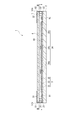
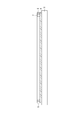
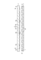
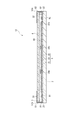
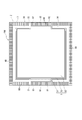
- FIG. 2 is a longitudinal sectional view taken along line II-II in FIG.
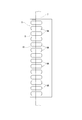
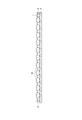
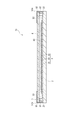
- FIG. 3 is a cross-sectional plan view taken along line III-III in FIG. 2.
- the longitudinal cross-sectional view which shows the example of the photoelectric conversion apparatus which formed the insulating film on the board
- the perspective view which shows the photoelectric conversion apparatus which concerns on 8th embodiment of this invention.
- the plane sectional view showing an example of the photoelectric conversion device concerning a ninth embodiment of the present invention.
- the plane sectional view showing another example of the photoelectric conversion device concerning a ninth embodiment of the present invention.
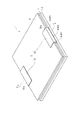
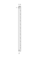
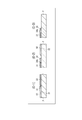
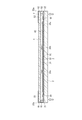
- FIG. 1 is a perspective view showing the entire photoelectric conversion apparatus according to the present embodiment.
- FIG. 2 is a longitudinal sectional view taken along the line II-II in FIG.
- FIG. 3 is a cross-sectional plan view taken along line III-III in FIG.
- the photoelectric conversion device 1 includes a substrate 2, a photoelectric conversion element 3 provided on the substrate 2, a sealing member 4 disposed above the substrate 2 and facing the substrate 2, and the sealing member 4.
- the extraction electrode 5 provided on the surface opposite to the surface facing the photoelectric conversion element 3, the side surface conductive portion 6 electrically connected to the extraction electrode 5, and provided outside the photoelectric conversion element 3
- An adhesive member 7 that bonds the substrate 2 and the sealing member 4, a substrate conductive portion 9 that is electrically connected to the photoelectric conversion element 3 and extends to the outside of the adhesive member 7, and an end of the substrate 2 rather than the adhesive member 7
- an electrical connection member 8 that electrically connects the side conductive part 6 and the board conductive part 9 on the part side.
- FIG. 2 is also a cross-sectional view of the photoelectric conversion device 1 in the thickness direction when the sealing member 4 is viewed with respect to the substrate 2, and FIG. 3 shows a direction along the surface of the substrate 2. It is also a plan sectional view when the cross section of the photoelectric conversion device 1 is viewed toward the substrate 2.
- 2 and 3 are also diagrams for explaining a structure for electrically connecting a photoelectric conversion element (organic EL element) 3 and an extraction electrode 5 described later.
- the substrate 2 is a smooth plate-like member for supporting the organic EL element 3 (photoelectric conversion element 3).
- the light-transmitting substrate 2 is used, and the light transmittance in the visible region of 400 to 700 nm is preferably 50% or more.
- a glass plate, a polymer plate, etc. are mentioned. Examples of the glass plate include soda lime glass, barium / strontium-containing glass, lead glass, aluminosilicate glass, borosilicate glass, barium borosilicate glass, and quartz.
- the substrate 2 is a translucent substrate, and the substrate 2 side is the light extraction direction of the organic EL element 3.
- an opaque substrate such as a silicon substrate or a metal substrate can be used in addition to the light-transmitting substrate 2.
- the portion of the substrate 2 that performs electrical extraction from the anode 31 of the organic EL element 3 is defined as a connection portion 21, and the portion that performs electrical extraction from the cathode 32 of the organic EL element 3 is connected. Part 22 is assumed.
- the substrate 2 when a plurality of photoelectric conversion devices 1 are arranged adjacent to each other, for example, a plate material having a vertical length of about 100 mm, a horizontal length of about 100 mm, and a thickness of about 0.7 mm is used. be able to.
- substrate 2 may cut out and use the board
- the organic EL element 3 includes an anode 31 as a first electrode 31 formed on the substrate 2, a cathode 32 as a second electrode 32 formed at a position facing the anode 31,
- the organic compound layer 33 is disposed between the anode 31 and the cathode 32. That is, the organic EL element 3 is configured such that the anode 31, the organic compound layer 33, and the cathode 32 are stacked in this order from the substrate 2 side.
- the organic EL element 3 may be configured with the first electrode 31 as a cathode and the second electrode 32 as an anode.
- the organic compound layer 33 may be composed of, for example, a single light emitting layer, or may be composed of various anode layers interposed between the anode 31 and the cathode 32 and the light emitting layer.
- the intermediate layer include a hole injection layer, a hole transport layer, an electron injection layer, and an electron transport layer.
- the organic compound layer 33 referred to in this embodiment refers to a layer including at least one layer composed of an organic compound.
- a known light emitting material such as Alq 3 is used for the light emitting layer, which has a structure showing monochromatic light such as red, green, blue, yellow, etc., or a light emitting color by a combination thereof, for example, a structure showing white light emission Etc. are used.
- a doping method is known in which a host is doped with a light emitting material as a dopant. In the light emitting layer formed by the doping method, excitons can be efficiently generated from the charge injected into the host. And the exciton energy of the produced
- a known electrode material is used, and when the light extraction direction is the substrate 2 side, for example, ITO (indium tin oxide), IZO (registered trademark) (indium zinc oxide), ZnO ( A transparent electrode material such as zinc oxide) is used.
- ITO indium tin oxide
- IZO registered trademark
- ZnO A transparent electrode material such as zinc oxide
- a known electrode material is used for the cathode 32, and when the light extraction direction is the substrate 2 side, a metal or an alloy can be used, for example, Ag or Al.
- a metal, an alloy, or the like is used for the anode 31, and a transparent electrode material is used for the cathode 32.
- auxiliary electrodes 34 (34a, 34b, 34c) are formed on the substrate 2 as shown in FIG.
- the auxiliary electrode 34 is provided so that a voltage drop due to the electrical resistance of the transparent electrode material used for the anode 31 is prevented, the voltage is uniformly supplied to the entire anode 31, and the organic EL element 3 emits light uniformly.
- the auxiliary electrode 34 is formed in a linear shape so as to be sandwiched between the substrate 2 and the anode 31.
- the auxiliary electrodes 34 are formed so as to extend in the vertical direction with respect to the paper surface of FIG. 2, and the auxiliary electrodes 34 are electrically connected to each other at a position not shown.
- a known electrode material is used for the auxiliary electrode 34, and a metal or an alloy can be used. For example, Cu, Ag, Al, or the like is used.
- the substrate conductive portion 9 includes a first substrate conductive portion 91 electrically connected to the anode 31 of the organic EL element 3 and a second substrate conductive portion 92 electrically connected to the cathode 32. Are provided on the substrate 2.
- the first substrate conductive portion 91 is connected to the end of the anode 31 and extends from the connection position to the end of the substrate 2 on the connection portion 21 side (left side in FIG. 2). 7 and an electrical connection member 8 (an electrical connection member 81 described later). More specifically, it passes between the adhesive member 7 and the electrical connection member 8 and the substrate 2.
- the second substrate conductive portion 92 is connected to the end portion of the cathode 32 and extends from the connection position to the end portion on the connection portion 22 side of the substrate 2 (the right side in FIG. 2). 7 and the electric connection member 8 (electric connection member 82 described later). More specifically, it passes between the adhesive member 7 and the electrical connection member 8 and the substrate 2.
- a known electrode material is used for the substrate conductive portion 9, and a metal or an alloy can be used. For example, Cu, Ag, Al, or the like is used. Note that the same material as the anode 31 and the cathode 32 can be used.
- the substrate conductive portion 9 has a width of about one-fourth to one-third of the length of one side when the substrate 2 is viewed in plan (connection with the anode 31 and the cathode 32). In a direction substantially orthogonal to the direction).
- the width of the substrate conductive portion is designed according to the amount of current required for the element.
- the substrate conductive portion 9 is connected to the auxiliary electrode 34 (not shown). For this reason, the present invention is not limited to display applications in which electrodes are arranged in a matrix, and even when a large amount of current is required to drive an organic EL element 3 for illumination, for example, in which electrodes are arranged in a plane, stable electrical Connection can be secured.
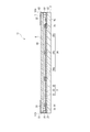
- FIG. 4 is a diagram when the substrate conductive portion 9 is viewed in plan, and only the substrate conductive portion 91 in FIG. 3 is taken out and illustrated. Therefore, the left long side of the substrate conductive portion 91 formed in a substantially rectangular shape in plan view is actually along the end portion of the substrate 2. Then, as shown in FIG. 4, a plurality of holes 9 ⁇ / b> A are formed side by side along the left long side of the substrate conductive portion 9. Further, the positions where the plurality of holes 9A are formed correspond to positions where an adhesive member 7 and an electrical connection member 8, which will be described later, shown by a two-dot chain line in FIG. 4 are provided, and the adhesive member 7 and the electrical connection member 8 are provided. It is formed so as to straddle.
- the substrate conductive portion 91 is illustrated and described, and the substrate conductive portion 92 is not illustrated, but the substrate conductive portion 92 is similarly formed with holes.
- Examples of the method for forming the holes 9A include mask sputtering.
- the hole 9 ⁇ / b> A is necessary when the adhesive member 7 and the electrical connection member 8 are heated and melted by laser irradiation to achieve bonding and electrical connection in the manufacturing process of the photoelectric conversion device 1. If the hole 9A is not formed in the substrate conductive portion 9, even if the laser is irradiated from the substrate 2 side, the heat from the laser irradiation is absorbed by the substrate conductive portion 9, and the adhesive member 7 and the electrical connection member 8 are heated. There is a risk that it will not melt.
- the hole 9A is formed, the laser passes through the hole 9A and reaches the adhesive member 7 and the electrical connection member 8. Therefore, the adhesive member 7 and the electrical connection member 8 are smoothly heated by the laser. And can be melted and joined and electrically connected. In particular, when the adhesive member 7 is melted and joined to the substrate 2, the sealing performance is improved. Note that the hole 9A is not shown in the substrate conductive portion 9 in other figures.
- An internal insulating film as an insulating film may be formed on the substrate conductive portion 9.
- the internal insulating film can prevent a short circuit between the cathode 32 and the substrate conductive portion 91 even when the cathode 32 is formed on the substrate conductive portion 91.
- an internal insulating film may be formed on the auxiliary electrode 34.
- the internal insulating film is formed on the auxiliary electrode 34 adjacent to the end portion of the anode 31, and is preferably formed on the auxiliary electrode 34c shown in FIG. If the internal insulating film is formed, a short circuit between the cathode 32 and the auxiliary electrode 34c can be prevented.
- the range for forming the internal insulating film is not limited to cover the whole of the substrate conductive portion 9 and the auxiliary electrode 34, but may be formed in a range that can prevent a short circuit.
- the substrate conductive portion 9 and the auxiliary electrode 34 may be formed. It may be formed on a part of the top.
- the internal insulating film may be made of an electrically insulating material.
- the internal insulating film can be formed using silicon oxide (SiO 2 ), aluminum oxide, or the like by mask vapor deposition or mask sputtering.
- the internal insulating film is preferably formed after the anode 31 is formed.
- the internal insulating film may be formed at a position where the short circuit between the anode 31 and the cathode 32 and the substrate conductive portion 9 and the auxiliary electrode 34 can be prevented, and a position where the electrical connection member 8 is not covered. That's fine.
- FIG. 5 is a cross-sectional view of the photoelectric conversion device 11 in which the internal insulating film 35 is formed on the substrate conductive portion 91 and the auxiliary electrode 34 c when viewed in the thickness direction with respect to the substrate 2 with the sealing member 4 facing upward. It is.
- the configuration of the photoelectric conversion device 11 has substantially the same configuration as that of the photoelectric conversion device 1, but the shape of the inner insulating film 35 and the shapes of the end portions of the anode 31, the cathode 32, and the organic compound layer 33 are the same. Different from the photoelectric conversion device 1.
- the cathode 32 extends further to the connection portion 21 side (left side in FIG.
- the internal insulating film 35 is formed on the substrate conductive portion 91, the internal insulating film 35 is interposed between the substrate conductive portion 91 and the cathode 32, and the electrical connection between the cathode 32 and the substrate conductive portion 91 is performed. Connection is prevented.
- the cathode 32 extends to the connection portion 22 side (the right side in FIG. 5) of the substrate 2, rides over the auxiliary electrode 34 c, and rides on the substrate conductive portion 92.
- the organic compound layer 33 is formed over the auxiliary electrode 34c, and the organic compound layer 33 is interposed between the auxiliary electrode 34c and the cathode 32.
- the organic compound layer 33 does not extend over the auxiliary electrode 34c, the cathode 32 and the auxiliary electrode 34c are electrically connected, and the cathode 32 and the anode 31 may be short-circuited. is there.
- the internal insulating film 35 is formed on the auxiliary electrode 34c, the internal insulating film 35 is interposed between the auxiliary electrode 34c and the cathode 32, and the electrical connection between the cathode 32 and the substrate conductive portion 92 is achieved. Connection is prevented.
- the anode 31 extends to the substrate conductive portion 92 and is electrically connected, if the internal insulating film 35 is formed on the substrate conductive portion 92, the anode 31 and the cathode are formed as described above. The short circuit with 32 can be prevented.
- the sealing member 4 is one of the members for sealing the organic EL element 3, and is a member that is disposed on the upper side of the organic EL element 3 so as to face the substrate 2 as shown in FIG.
- the organic EL element 3 is sealed as follows. First, the substrate 2 is disposed below the organic EL element 3, and the sealing member 4 is disposed above the organic EL element 3. When the photoelectric conversion device 1 is viewed in cross-section in the substrate thickness direction as shown in FIG. 2, the photoelectric conversion device 1 is disposed outside the organic compound layer 33 of the organic EL element 3 as shown in FIG.
- the adhesive member 7 is provided so as to surround the periphery of the organic compound layer 33 in a frame shape when viewed in cross-section in the direction along the surface 2.
- the sealing member 4 is preferably a plate-like, film-like, or foil-like member. Specifically, a glass plate, a polymer plate, a film, a metal plate, a metal foil, etc. are mentioned.
- the plate-shaped member is used for the sealing member 4 in this embodiment, for example, a cap-shaped object or a plate-shaped object (for example, a seat) having a recess having an inner dimension larger than the outer dimension of the organic EL element 3 is used. (Grid substrate), sheet-like material or film-like material.
- the sealing member 4 is preferably formed to be the same as the substrate 2 or smaller than the substrate 2.
- the sealing member 4 is bonded to the substrate 2 when the photoelectric conversion device 1 is viewed in plan view.
- the thickness of the side conductive portion 6 is preferably the same as the thickness of the side conductive portion 6 relative to the end of 2, or offset so as to be slightly inside.
- the offset dimension may not be the entire sealing member 4, and corresponds to the connection portion 21 and the connection portion 22 of the substrate 2 when the substrate 2 and the sealing member 4 are joined. Only a part may be sufficient.
- the thickness dimension of the sealing member 4 is preferably 0.1 mm or more and 5 mm or less. If the thickness dimension is 0.1 mm or less, the air permeability increases and the sealing performance decreases.
- the extraction electrode 5 is an electrode for electrically extracting the electrodes 31 and 32 of the photoelectric conversion element 3 sealed inside the photoelectric conversion device 1 to the outer surface side of the photoelectric conversion device 1.
- the sealing member 4 is provided on the surface opposite to the surface facing the organic EL element 3.
- the extraction electrode 5 is a part for connecting wiring from an external power source for applying a voltage to the anode 31 and the cathode 32.
- the extraction electrode 5 is a portion for connecting a wiring to an external device in order to extract the electric charge generated by the solar cell element to the outside. As shown in FIGS.
- the extraction electrode 5 is a pair of electrodes of a first extraction electrode 51 and a second extraction electrode 52 on the surface opposite to the surface facing the organic EL element 3 of the sealing member 4. It is provided as. And the 1st extraction electrode 51 and the 2nd extraction electrode 52 have protrusion part 51a, 52a which protrudes outside from the edge part of the sealing member 4, respectively.
- the first extraction electrode 51 and the second extraction electrode 52 are electrically connected to the anode 31 and the cathode 32 via the side surface conductive portion 6, the electrical connection member 8, and the substrate conductive portion 9, respectively. ing.
- the positions and shapes of the first extraction electrode 51 and the second extraction electrode 52 are formed so as to correspond to the connection portions 21 and 22 of the substrate 2 as shown in FIGS.
- the sealing member 4 is formed to be smaller than the substrate 2 by a predetermined dimension, and the protruding portions 51a and 52a are substantially flush with the side surface of the substrate 2 as shown in FIG. Is provided.
- the side surface conductive portion 6 is a portion that is disposed on the side surface of the photoelectric conversion device and ensures electrical connection between the extraction electrode 5 and the organic EL element 3.
- the side conductive portion 6 is provided outside the end portion of the sealing member 4 and is electrically connected to the extraction electrode 5.
- the side surface conductive portion 6 includes side surface conductive portions 61 and 62 that are electrically connected to the protruding portions 51a and 52a in the vertical direction.
- the side surface conductive portion 6 is formed integrally with the extraction electrode 5, and the side surface conductive portion 6 is formed so as to cover the end surface of the sealing member 4. And the front-end
- the sealing member 4 is formed to be smaller than the substrate 2 by a predetermined dimension, and the side surface conductive portions 61 and 62 are substantially flush with the side surface of the substrate 2 as shown in FIG. It is provided as follows. By doing in this way, when arrange
- the adhesive member 7 is one of the members for sealing the organic EL element 3 and joins the substrate 2 and the sealing member 4. And the adhesive member 7 can seal an organic compound layer by forming in the frame shape around the organic compound layer 33, as shown in FIG. As shown in FIG. 2, in the portion where the substrate conductive portion 9 is formed, the adhesive member 7 joins the substrate 2 and the sealing member 4 across the substrate conductive portion 9.
- the position (bonding position) where the adhesive member 7 is provided depends on the size of the substrate 2 and the space where the electrical connection member 8 is provided, but in order to widen the area where the organic EL element 3 can be set, The side is preferred.
- the distance from the end of the substrate 2 to the adhesive member 7 is 0.1 mm or more and 0. .3 mm or less is particularly preferable.
- the adhesive member 7 is preferably made of an inorganic compound from the viewpoints of sealing properties, moisture resistance, and bonding strength.
- Low melting glass is preferred because it can be formed by laser irradiation.
- the low melting point in the present invention means that having a melting point of 650 ° C. or lower.
- the melting point is preferably 300 ° C. or higher and 600 ° C. or lower.
- the low-melting glass preferably includes a transition metal oxide capable of bonding glass and metal, a rare earth oxide, and the like, and more preferably powder glass (frit glass).
- powder glass powder glass
- the substrate 2 and the sealing member 4 cover the upper and lower sides of the organic EL element 3, the adhesive member 7 surrounds the periphery of the organic EL element 3, and the substrate 2 and the sealing member 4 are joined. By doing so, the organic EL element 3 is sealed. At this time, a space surrounded by the substrate 2, the sealing member 4, and the adhesive member 7 is a sealing space S. In addition to the organic EL element 3 being provided in the sealed space S, the heat dissipation member 43 is filled.
- the heat radiating member 43 plays a role of efficiently transmitting heat generated in the organic EL element 3 to the sealing member 4 side.
- an inactive member having good thermal conductivity is preferable, and for example, fluorine oil can be used.
- the electrical connection member 8 is one of members for electrically connecting the side surface conductive portion 6 and the substrate conductive portion 9 to ensure electrical connection from the extraction electrode 5 to the organic EL element 3. As shown in FIGS. 2 and 3, the electrical connection member 8 is provided on the outer side (the end portion side of the substrate 2) than the adhesive member 7. An electrical connection member 81 is connected to the side conductive part 61 and the board conductive part 91, and an electrical connection member 82 is connected to the side conductive part 62 and the board conductive part 92. As shown in FIG. 2, each of the electrical connection members 81 and 82 has the electrical connection member 8 in a space between the adhesive member 7 and the side surface conductive portions 61 and 62. Further, as shown in FIG.
- the electrical connection members 81 and 82 are electrically connected to the substrate conductive portions 91 and 92 in the vertical direction, respectively, and the substrate is connected to the inside of the side surface conductive portions 61 and 62, respectively. Electrical connection is made in the direction along the surface of 2. Further, as shown in FIG. 3, the electrical connection members 81 and 82 are provided with substantially the same width as the widths of the substrate conductive portions 91 and 92. Therefore, a wide electrical continuity can be obtained, so that a stable electrical connection can be ensured.
- a conductive adhesive or a solder material can be used as the electrical connection member 8.
- a low melting point solder material having a melting point of 300 ° C. or lower is preferable.
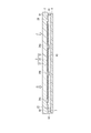
- FIG. 6A is a schematic view showing the manufacturing process on the sealing member 4 side.
- 6A to 6C are views showing a cross section in the thickness direction of the sealing member 4, and show a case where an adhesive member 7 or the like is applied on the sealing member 4.
- FIG. 6A the adhesive member 7 is applied on one surface of the sealing member 4.
- frit glass is used as the adhesive member 7.
- the application position of the adhesive member 7 is the end side of the sealing member 4, and when bonded to the substrate 2, the bonding position surrounds the organic compound layer 33 in a frame shape as shown in FIG.
- variety of the adhesive member 7 may become a joining width which can ensure joining strength.
- the application method include a dispenser method.
- the electrical connection member 8 is applied to the end side of the sealing member 4 with respect to the adhesive member 7.
- a low melting point solder material is used as the electrical connection member 8.
- the application position of the electrical connection member 8 is a position corresponding to a site where electrical connection with the substrate conductive portion 9 is performed. Examples of the application method include a dispenser method.
- the adhesive member 7 and the electrical connection member 8 used here are pasty at the time of application, and each contains an alcohol component.
- a heating means H such as a hot plate is disposed on the surface opposite to the surface of the sealing member 4 to which the adhesive member 7 and the electrical connection member 8 are applied.
- the sealing member 4 is heated from the surface and fired. By this baking, the above-mentioned alcohol component contained in the adhesive member 7 and the electrical connection member 8 is removed.
- a heating method it is good also as a method of putting the said sealing member 4 in a heating furnace.
- a heat radiation member 43 is applied on the surface of the sealing member 4 to which the adhesive member 7 and the electrical connection member 8 are applied. Examples of the application method include a dispenser method.
- FIG. 7A to 7D are schematic diagrams for explaining a manufacturing process on the substrate 2 side in the photoelectric conversion device 1.
- FIG. 7A to 7D are views showing a cross section in the thickness direction of the substrate 2, and show a case where the organic EL element 3 is formed on the substrate 2.
- FIG. 7A to FIG. 7D alphabets and numbers are given according to the parts of the substrate 2. The alphabet indicates each manufacturing process on the substrate 2 side, the numeral 1 indicates that the periphery of the connection portion 21 on the left side of FIG. 2 is indicated, and 2 indicates that the periphery of the connection portion 22 on the right side of FIG. Represents a peripheral portion of the substrate 2 other than the connection portions 21 and 22.
- auxiliary electrodes 34a, 34b, 34c (only the auxiliary electrode 34c is shown in the figure) and substrate conductive portions 91, 92 are formed on the substrate 2.
- the substrate conductive portions 91 and 92 are formed by a mask sputtering method or the like so that the above-described hole 9A (see FIG. 4) is formed.
- the anode 31 is formed on the substrate 2.
- a known method such as vacuum deposition or sputtering can be employed.
- auxiliary electrode 34c is in contact with the anode 31 on the side surface.
- the outer edge of the anode 31 is formed to extend to the substrate conductive portion 91, and in FIG. 7B (B-2) and (B-3). As shown, it is formed in a region inside the substrate 2 with respect to the auxiliary electrode 34c.
- the organic compound layer 33 is formed on the anode 31.
- a forming method a known method such as a dry film forming method such as vacuum deposition, sputtering, plasma, or ion plating, or a wet film forming method such as spin coating, dipping, flow coating, or ink jet can be employed.
- a masking means it is preferable to perform layer formation by applying a masking means so that the organic compound layer 33 is formed at a predetermined position. As shown in (C-2) of FIG.
- the end of the organic compound layer 33 on the substrate conductive portion 92 side passes over the auxiliary electrode 34c, and the substrate 2 between the auxiliary electrode 34c and the substrate conductive portion 92 is placed. It extends to the part where the surface is exposed.
- the end portion of the organic compound layer 33 on the substrate conductive portion 91 side is offset to a region inside the end portion of the anode 31 on the substrate conductive portion 91 side. Is formed.
- the cathode 32 is formed on the organic compound layer 33.
- a known method such as vacuum deposition or sputtering can be employed.
- mask sputtering or the like is preferably performed so that the cathode 32 is formed at a predetermined position.
- the end of the cathode 32 on the substrate conductive portion 92 side is formed so as to extend over the auxiliary electrode 34c and further onto the substrate conductive portion 92.
- the end portion of the cathode 32 on the substrate conductive portion 91 side is less than the end portion of the organic compound layer 33 on the substrate conductive portion 91 side so as not to be short-circuited. It is offset and formed inside.
- FIGS. 8A to 8C are schematic views for explaining a process of bonding the sealing member 4 side and the substrate 2 side manufactured in the above process.
- FIGS. 8A to 8C are views of the cross section in the thickness direction of the substrate 2 and the sealing member 4, and show the case where the substrate 2 and the sealing member 4 are bonded in the vertical direction.
- the surface of the sealing member 4 on which the adhesive member 7 and the electrical connection member 8 are applied is directed upward, and the surface of the substrate 2 on which the organic EL element 3 is formed is directed downward.
- FIG. 8B the sealing member 4 is pressed in the direction of the arrow, and the heat dissipating member 43 applied on the sealing member 4 is stretched and filled in the sealing space S.
- the first extraction electrode 51 and the second extraction electrode 52 are formed on the sealing member 4 with the sealing member 4 facing upward.
- the metal foil is processed and formed in advance by press molding so that the side conductive parts 61 and 62 are formed, and the metal foil is fixed to the sealing member 4 with an epoxy resin. The side conductive parts 61 and 62 are brought into contact with the electrical connection member 8.
- the bonded portion is locally heated by laser irradiation or the like in the arrow direction while maintaining the contacted state, and the adhesive member 7 and the electrical connection member 8 are melted and heated.
- the adhesive member 7 and the electrical connection member 8 are bonded to members that are in contact with them.
- the laser output and the laser moving speed are adjusted so that the temperature of the adhesive member 7 becomes 600 ° C.
- the adhesive member 7 made of frit glass surrounds the outside of the organic compound layer 33 of the organic EL element 3 in a frame shape, and the substrate 2 and the sealing member 4 are bonded.
- the photoelectric conversion device 1 having a narrow frame structure having high bonding strength and excellent sealing performance can be obtained.
- An electrical connection member 8 is provided at a position further outside the adhesive member 7, and the electrical connection member 8 is electrically connected to the inner side of the side surface conductive portion 6, and is vertically connected to the substrate conductive portion 9. Since electrical connection is made in the direction, stable electrical connection can be ensured. Moreover, by providing the electrical connection member 8 inside the side surface conductive portion 6, blurring of the electrical connection member 8 before laser processing is suppressed, and the manufacturing yield of the photoelectric conversion device 1 is improved.
- the organic EL element 3 is electrically connected to the extraction electrode 5 through the substrate conductive portion 9, the electrical connection member 8, and the side surface conductive portion 6, and the extraction electrode 5 is in the thickness direction of the substrate 2. Therefore, the gap between the photoelectric conversion devices 1 can be narrowed and the joint between the devices becomes inconspicuous.
- the electrical connection member 8 Since the electrical connection member 8 is provided in the space between the adhesive member 7 and the side surface conductive portion 6, the electrical connection member 8 on the end portion side of the substrate 2 is well accommodated in the photoelectric conversion device 1.
- the electric connection member 8 does not protrude outside the side surface conductive portion 6. Therefore, even when a plurality of photoelectric conversion devices 1 are arranged adjacent to each other, the electrical connection members 8 that protrude from the end side of the substrate 2 do not interfere with each other, and also from this point, the intervals between the photoelectric conversion devices 1 are reduced. And the joint between the photoelectric conversion devices 1 becomes inconspicuous.
- first extraction electrode 51 and the side surface conductive portion 61 are configured by one member, and the second extraction electrode 52 and the side surface conductive portion 62 are configured by one member, electrical extraction from the organic EL element 3 is performed.
- the number of members necessary for the process can be reduced, and the structure and manufacturing process of the photoelectric conversion device 1 can be simplified.
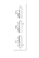
- FIG. 9 is a cross-sectional view of a cross section in the thickness direction of the photoelectric conversion device 12 according to the second embodiment.
- the photoelectric conversion device 12 according to the second embodiment differs from the photoelectric conversion device 1 according to the first embodiment in the method of joining the side surface conductive portion 6 and the electrical connection member 8. That is, the side surface conductive portions 61 and 62 protrude to positions where they face the substrate conductive portions 91 and 92 on the end side of the substrate 2, respectively, and the tips (lower ends in FIG.
- the electrical connection member 8 is not provided in a space formed between the outside of the adhesive member 7 and the inside of the side surface conductive portion 6, and as shown in FIG. In addition, an electrical connection is made in the vertical direction with respect to the side surface conductive portion 6. Therefore, the joining position by the adhesive member 7 is further provided on the end side of the substrate 2 as compared with the case of the first embodiment.
- the same effects as (1) to (3) and (5) to (7) in the first embodiment are exhibited, and the following effects are also achieved.
- (8) The space for providing the electrical connection member 8 formed between the outside of the adhesive member 7 and the inside of the side surface conductive portion 6 is reduced, and the adhesive member 7 is further provided on the outer side (end side of the substrate 2). I can do it. Therefore, the space on the substrate 2 for arranging the organic EL element 3 can be further widened while ensuring the reliability of conduction between the side surface conductive portion 6 and the substrate conductive portion 9, resulting in a larger light emitting area. I can do it.
- FIG. 10 is a cross-sectional view of a cross section in the thickness direction of the photoelectric conversion device 13 according to the third embodiment.
- the photoelectric conversion device 13 according to the third embodiment is different from the photoelectric conversion device 1 according to the first embodiment in the structure of the extraction electrode 5 and the side surface conductive portion 6. That is, the extraction electrode 5 and the side conductive portion 6 are configured separately.
- the same material as that described in the first embodiment can be used as the material that can be used for the extraction electrode 5 and the side surface conductive portion 6.
- the extraction electrode 5 and the side surface conductive part 6 may be comprised with the same member, and may be comprised with a different member. Examples of a method for connecting the extraction electrode 5 and the side conductive portion 6 include solder connection, fusion, and welding.
- the members constituting the first extraction electrode 51 and the second extraction electrode 52 are bent at the end side of the sealing member 4 to form the side conductive portions 61 and 62. Since it is difficult to perform the processing, it is easy to manufacture the photoelectric conversion device in which the sealing member is thin by configuring the side surface conductive portions 61 and 62 as separate members.
- FIG. 11 is a cross-sectional view of a cross section in the thickness direction of the photoelectric conversion device 14 according to the fourth embodiment.
- the photoelectric conversion device 14 according to the fourth embodiment is different from the photoelectric conversion device 13 in the electrical connection structure of the electrical connection member 8 in the photoelectric conversion device 13 according to the third embodiment.
- the side conductive parts 61 and 62 are electrically connected in the vertical direction to the protruding parts 51a and 52a of the extraction electrodes 51 and 52, respectively, and are electrically connected in the vertical direction to the substrate conductive parts 91 and 92, respectively.
- the side conductive parts 61 and 62 may be formed of the same member as the electrical connection member 8 described above.
- the adhesive member 7 is further provided in comparison with the first embodiment and the third embodiment. It can be provided on the outside (the end side of the substrate 2). Therefore, the space on the substrate 2 for disposing the organic EL element 3 can be further increased, and as a result, the light emitting area and the like can be further increased.
- the side conductive parts 61 and 62 are formed by bending the members constituting the first extraction electrode 51 and the second extraction electrode 52 on the end side of the sealing member 4.
- this connection structure in which the first extraction electrode 51 and the second extraction electrode 52 are directly connected to the extraction electrode by the side conductive parts 61 and 62 separate from each other is necessarily effective.
- a low melting point metal is used for the side conductive parts 61 and 62, for example, if the sealing member 4 has a thickness of about 1 mm, the low melting point metal can be easily disposed on the side conductive parts 61 and 62. And electrical continuity can be ensured.
- FIG. 12 is a cross-sectional view of a cross section in the thickness direction of the photoelectric conversion device 15 according to the fifth embodiment.
- the photoelectric conversion device 15 according to the fifth embodiment is different from the photoelectric conversion device 13 according to the third embodiment in that the anode 31 and the cathode 32 of the organic EL element 3 are extended to the end side of the substrate 2. Different from the converter 13.
- FIG. 13 is a cross-sectional view of a cross section in the thickness direction of the photoelectric conversion device 16 according to the sixth embodiment.
- the photoelectric conversion device 16 according to the sixth embodiment is different from the photoelectric conversion device 14 according to the fourth embodiment in that the anode 31 and the cathode 32 of the organic EL element 3 are extended to the end side of the substrate 2. Different from the photoelectric conversion device 14.
- FIG. 14 is a cross-sectional view of a cross section in the thickness direction of the photoelectric conversion device 17 according to the seventh embodiment.
- the photoelectric conversion device 17 according to the seventh embodiment is such that the sealing member 4 is a conductive sealing member 41 in the photoelectric conversion device 1 according to the first embodiment.
- the second extraction electrode 52, the side conductive portion 62, and the portion where the electrical connection member 82 and the conductive sealing member 41 are in contact with each other are externally insulated as an insulating portion so as not to contact each other and to be short-circuited.
- a layer 42 is provided. As shown in FIG. 14, the outer insulating layer 42 extends from the upper surface of the conductive sealing member 41 to the lower surface through the side surface.
- the anode 31 of the organic EL element 3 is electrically connected to the first extraction electrode 51 via the substrate conductive portion 91, the electrical connection member 81, and the side surface conductive portion 61, and the first extraction electrode 51 is electrically conductive.
- the sealing member 41 is connected.
- the connection between the first extraction electrode 51 and the conductive sealing member 41 only needs to be connected in a state where conduction is ensured.
- the conductive sealing member 41 may be any member having conductivity, and for example, a metal plate or foil can be used. Moreover, as long as the surface of the sealing member 4 is covered with a conductive material, the sealing member 4 itself may not be conductive.
- the outer insulating layer 42 may be formed of an electrically insulating material.
- the external insulating layer 42 can be formed of silicon oxide (SiO 2 ), aluminum oxide, or the like by a mask vapor deposition method, a mask sputtering method, or the like. Alternatively, an insulating film, a foil, or the like can be attached to the conductive sealing member 41 and formed.
- the sealing member 4 in the photoelectric conversion device 17 is the conductive sealing member 41, and the anode 31 of the organic EL element 3 is electrically connected to the first extraction electrode 51 through the electrical connection member 8 and the like. Further, it is electrically connected to the conductive sealing member 41. Therefore, the wiring from the external power supply on the anode 31 side can be connected not only to the first extraction electrode 51 but also to the conductive sealing member 41, and flexibility in the electrical connection position occurs.
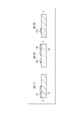
- FIG. 15 is a perspective view showing the photoelectric conversion device 18 provided with a plurality of first extraction electrodes 51 and second extraction electrodes 52.
- the photoelectric conversion device 18 according to the eighth embodiment is the same as the photoelectric conversion device 1 according to the first embodiment in that two first extraction electrodes 51 and two second extraction electrodes 52 are provided. Different from 1.
- the present invention not only the pair of the first extraction electrode 51 and the second extraction electrode 52 is provided, but also the first extraction electrode 51 and the second extraction electrode as in the above-described embodiment.
- a plurality of at least one of 52 may be provided. Since the extraction electrode 5 reduces the sheet resistance of the first electrode or the second electrode, it is preferable to provide a plurality of extraction electrodes 5 because the sheet resistance can be further reduced. Of the first electrode or the second electrode, it is preferable to provide more extraction electrodes that are electrically connected to the one using a transparent electrode such as ITO having a high sheet resistance, or a larger electrode area.
- the anode as the first electrode is a transparent electrode made of ITO
- the cathode as the second electrode is an electrode made of aluminum.
- the area of the first extraction electrode 51 connected to the anode is made larger than that of the second extraction electrode 52 in order to reduce the sheet resistance of the anode (FIG. 15). reference). From the viewpoint of preventing light emission unevenness, it is effective to increase the number of first extraction electrodes 51 compared to the number of second extraction electrodes 52 in order to suppress a voltage drop due to ITO having a high sheet resistance.
- FIG. 16 is a plan cross-sectional view of a cross section of the photoelectric conversion device 19 ⁇ / b> A in a direction along the surface of the substrate 2 as viewed toward the substrate 2.
- FIG. 17 is a plan cross-sectional view of a cross section of the photoelectric conversion device 19 ⁇ / b> B in the direction along the surface of the substrate 2 as viewed toward the substrate 2.
- the photoelectric conversion devices 19 ⁇ / b> A and 19 ⁇ / b> B according to the ninth embodiment are different from the photoelectric conversion device 1 in that the light reflection unit 36 is provided on the substrate 2 in the photoelectric conversion device 1 according to the first embodiment.
- 16 and 17 is substantially the same as the position of FIG. 3 according to the first embodiment.
- the side conductive parts 61 and 62, the adhesive member 7, and the electrical connection members 81 and 82 are indicated by two-dot chain lines for convenience of explanation.
- the light reflecting portion 36 is a layer that is made of a material that reflects light and reflects light generated in the organic compound layer 33 in the light extraction direction.
- the light reflecting portion 36 is formed, for example, by forming a metal film by vapor deposition or attaching a metal foil or a metal plate.
- substrate conductive part 9 is comprised with metals, such as Al, Cu, Ag, it is preferable to form the light reflection part 36 with the same member as the said board
- the light reflecting portion 36 is provided at a position different from the position where the substrate conductive portion 9, the auxiliary electrode 34, and the organic EL element 3 are formed on the substrate 2. Further, it is preferably provided over the entire position different from the position where the substrate conductive portion 9, the auxiliary electrode 34, and the organic EL element 3 are formed. Therefore, any one of the substrate conductive portion 91, the substrate conductive portion 92, and the auxiliary electrode may be formed integrally with the light reflecting portion 36 so that the area of the light reflecting portion 36 is as large as possible.
- the light reflecting portion 36 is composed of a conductive member
- the anode 31 of the organic EL element 3 and Since the cathode 32 may be short-circuited a short-circuit is caused by providing a predetermined dimensional gap between the light reflecting portion 36 and one of the substrate conductive portion 91 and the substrate conductive portion 92 or by interposing an insulating material. It is preferable to prevent.
- a plurality of holes 9 ⁇ / b> A are formed along the edge of the substrate 2 in the substrate conductive portion 9 and the light reflecting portion 36 of the photoelectric conversion device 19 ⁇ / b> A. That is, the hole 9 ⁇ / b> A of the substrate conductive portion 9 described in the first embodiment is also formed in the light reflecting portion 36.
- the substrate conductive portion 9 and the light reflecting portion 36 are formed simultaneously.
- the substrate conductive portion 9 and the light reflecting portion 36 are formed by the sputtering method or the like using the same metal material (Al or the like), and then pattern etching is performed to form the hole 9A.
- the hole 9A is formed in a substantially elliptical shape.
- a plurality of holes 9 ⁇ / b> B having a shape different from the above-described hole 9 ⁇ / b> A are formed in the substrate conductive portion 9 and the light reflecting portion 36 along the end portion of the substrate 2. .
- the substrate conductive portion 9 and the light reflecting portion 36 are simultaneously formed in the same manner as the photoelectric conversion device 19A.
- the substrate conductive portion 9 and the light reflecting portion 36 are formed in a state having the holes 9B in advance by a mask sputtering method or the like.
- the hole 9 ⁇ / b> B is formed in a substantially rectangular shape and extends inward from the end of the substrate 2.
- the hole 9B is also provided for smooth joining by laser irradiation.
- the same effects as (1) to (7) in the first embodiment are exhibited, and the following effects are also achieved.
- the light emitted from the organic compound layer 33 of the organic EL element 3 is emitted from the substrate 2 as it is in the light extraction direction without propagating through the substrate 2 or is transmitted from the substrate 2 through propagation in the substrate 2.
- the light is emitted in the extraction direction or in the opposite direction.
- the light reflecting portion 36 is provided on the substrate 2 as described above and at a position different from the position where the substrate conductive portion 9 and the like are provided.
- the emitted light that has propagated through the substrate 2 to the provided position is not emitted in the direction opposite to the light extraction direction, but is reflected in the light extraction direction.
- the light reflected in this way is emitted in the light extraction direction, or further propagated toward the end portion of the substrate 2 while being reflected and then emitted in the light extraction direction.
- the light reflection part 36 is formed on the board
- emitted from the organic EL element 3 reaches the junction part in the edge part side of the board
- the said junction part is concealed with light, when the photoelectric conversion devices 19A and 19B are arranged adjacent to each other, the joints and junctions between the photoelectric conversion devices 19A and 19B become less conspicuous.
- the junction can be hidden by light, a structure that improves the junction strength by increasing the junction width of the junction is possible, and the degree of freedom in designing the photoelectric conversion device increases.
- the photoelectric conversion element 3 used in the photoelectric conversion device 1 the organic EL element 3 has been described as an example in the embodiment.
- the photoelectric conversion element 3 is not limited to this, and the organic thin film solar cell element, the dye-sensitized solar cell element, and the like are airtight. Applies to elements that need to be held.
- an organic thin film solar cell element when the substrate 2 side is a light incident surface, a transparent conductive film, a P-type organic semiconductor, an N-type organic semiconductor, and a conductive film are stacked in this order from the substrate 2 side. be able to.
- a transparent electrode member can be used so that light from the substrate 2 side can reach the solar cell layer (P-type organic semiconductor and N-type organic semiconductor).
- P-type organic semiconductor and N-type organic semiconductor For example, ITO (indium tin oxide), ZnO A transparent electrode such as (zinc oxide) or SnO 2 (tin oxide) can be used.
- a metal electrode such as aluminum, gold, silver, or titanium that has low light absorption and high reflection can be used as the reflective film.
- Other configurations can be the same as those in the above embodiment.
- this invention is not limited to the said embodiment,
- transformation shown below is included in the range which can achieve the objective of this invention.
- the sealed space S may be evacuated or filled with a dry gas or the like.
- the external insulating layer 42 may be provided also in a portion where the first extraction electrode 51 and the side surface conductive portion 61 and the conductive sealing member 41 are in contact with each other.
- At least one of the first electrode and the second electrode is connected by the above-described electrical connection structure according to the present invention.
- at least one of the plurality of electrodes is connected by the above-described electrical connection structure according to the present invention. It only has to be done.
- the number, position, area, and the like of the extraction electrode 5 are not limited to the positions described in the above embodiment.
- the first extraction electrode 51 and the second extraction electrode 52 are provided along two opposing sides of the sealing member 4, but the first extraction electrode 51 is provided on each of two adjacent sides of the sealing member 4.
- a second extraction electrode 52 may be provided.
- the 1st extraction electrode 51 and the 2nd extraction electrode 52 are provided in the corner
- a plurality of extraction electrodes 5 are provided, they do not have to have the same area, and can be set as appropriate from the viewpoints of components of the first electrode and the second electrode that are electrically connected.
- a light diffusion layer may be provided on the entire surface of the substrate 2 facing the outside of the photoelectric conversion device or partially. Light emitted from the organic compound layer 33 of the organic EL element 3 can be efficiently extracted outside in the light extraction direction.
- the light diffusion layer is provided by attaching a light diffusion film, vapor deposition, or the like.
- the anode 31 and the cathode 32 are extended to the end portion side of the substrate 2 (see FIG. 12), and after the extension, the anode 31 and the cathode 32 are connected to the substrate end portion side.
- the above-described substrate conductive portion may be further formed between the cathode 32 and the substrate 2.
- the photoelectric conversion device 1 was created based on the configuration of the first embodiment, a drive test was performed, and the evaluation was performed.
- the evaluation items are as follows.
- Device lifetime Evaluate the time to halve the initial luminance. This half time represents the sealing performance in the photoelectric conversion device.
- the driving test was performed under the following conditions. A voltage was applied to the organic EL element 3 so that the current value was 1 mA / cm 2, and the voltage value at that time was measured. Further, the EL emission spectrum at that time was measured with a spectral radiance meter (CS-1000: manufactured by Comica Minolta). From the obtained spectral radiance spectrum, luminance, chromaticity, current efficiency (cd / A), external quantum efficiency (%), and main peak wavelength (nm) were calculated. Further, a continuous DC current test was performed at an initial luminance of 5000 cd / m 2 (nit), and the half life of the device was measured.
- CS-1000 spectral radiance meter
- the structure and member of the photoelectric conversion apparatus used for the drive test are as follows.
- -Substrate Blue plate glass (100 mm x 100 mm, thickness: 0.7 mm)
- Sealing member soda glass (99.95 mm ⁇ 100 mm, thickness: 0.7 mm)
- Extraction electrode Copper foil (thickness 0.08mm)
- Adhesive member frit glass (AGC, AP5346B, melting point 485 ° C.)
- Electrical connection member Solder material (Ishikawa Metals, J3-3230-LU, melting point 300 ° C.)
- Heat dissipation member Fluorine oil (Daikin Industries, demnum grease S-200)
- Auxiliary electrode, substrate conductive part APC Organic EL device configuration: anode (ITO.
- Thickness 100 nm) / NPD (thickness: 50 nm) / Alq (thickness 60 nm) / LiF (thickness: 1 nm) / cathode (Al. Thickness: 100 nm) NPD was formed as a hole transport layer, Alq was formed as a light emitting layer, and LiF was formed as an electron injecting electrode (cathode).
- -Adhesive member width 0.7 mm ⁇ Distance from the edge of the substrate to the adhesive member: 0.2 mm ⁇ Width of substrate conductive part: 20mm
- the performance of the photoelectric conversion device created based on the configuration of the first embodiment is as follows.
- the performance of the organic EL element provided in the photoelectric conversion device was as follows.
- Luminance 305 cd / m 2
- Photoelectric conversion device 2 Substrate 3 Photoelectric conversion element (organic EL element) 31 First electrode (anode) 32 Second electrode (cathode) 33 Organic compound layer 35 Insulating film (internal insulating film) 36 Light reflection part 4 Sealing member 42 Insulation part (external insulation layer) 5 Extraction electrode 51 1st extraction electrode 52 2nd extraction electrode 51a, 52a Protrusion part 6, 61, 62 Side surface conductive part 7 Adhesive member 8, 81, 82 Electrical connection member 9, 91, 92 Substrate conductive part
Abstract
Description
このような光電変換素子においては、水や空気が素子寿命などの性能に大きく影響を及ぼすため、光電変換素子を水や空気から守るための封止構造が検討されている。 A photoelectric conversion device including a photoelectric conversion element having an organic compound layer between a pair of electrodes formed on a substrate has been proposed. As a photoelectric conversion element, for example, an organic electroluminescence element (hereinafter referred to as an organic EL element), An organic thin film solar cell element etc. can be mentioned. An organic EL element converts electricity into light, and an organic thin film solar cell element is an element that converts light into electricity.
In such a photoelectric conversion element, since water and air greatly affect performance such as element lifetime, a sealing structure for protecting the photoelectric conversion element from water and air has been studied.
しかしながら、特許文献1に記載された有機EL発光装置は、透明基板及び金属枠体の接合と金属枠体及び金属製保護蓋の接合といったように、接合すべき箇所が多いため、接合不足が生じる可能性が高く、有機EL発光積層体を十分に封止できないおそれがあった。
さらに、透明基板に形成した貫通孔を介して電気的接続端子と有機EL発光積層体の電極とを接続しているため、発光面積を大きくすることができないという問題があった。
ここで、特許文献1には、別の有機EL発光装置の実施の形態として、透明基板に貫通孔を形成しない形態も開示されている。この実施の形態では、透明基板表面に対して水平な方向へ電気接続端子を取り出している。しかし、このような形態だと複数の有機EL発光装置を互いに隣接させて配置させようとすると、隣り合う有機EL発光装置の電気接続端子が干渉し合う。そのため、有機EL発光装置間の間隔を狭くして隣接配置させることができない。 For example, an organic electroluminescence light emitting device (hereinafter referred to as an organic EL light emitting device) described in
However, the organic EL light-emitting device described in
Furthermore, since the electrical connection terminal and the electrode of the organic EL light emitting laminate are connected through a through hole formed in the transparent substrate, there is a problem that the light emitting area cannot be increased.
Here,
このような構造とすることで、複数の表示パネルを隣接させて配置させた場合でも、表示パネル同士の継ぎ目部分が目立たなくなるとされている。 For such a problem, for example,
By adopting such a structure, even when a plurality of display panels are arranged adjacent to each other, the joint portion between the display panels becomes inconspicuous.
すなわち、有機EL素子等を駆動させる際に必要とされる電流量は、面状発光タイプの有機EL素子等の方が表示パネル用途に比べて多くなる。そのため、特許文献2に記載された接続スペーサーを用いた表示パネル用の接続技術では、信号電極等と接続されるITOパッドと接続スペーサー中の導電性微小球とが接触する面積、または取出し電極と当該導電性微小球とが接触する面積が小さく、さらに当該接触が不均一になることから多くの電流量を必要とする有機EL照明パネル等において安定した電気的接続を確保し難い。さらに、特許文献2に記載の技術は、接続スペーサーとして、導電性微小球を電気絶縁性樹脂で被覆したもの等を用いているため、導電性微小球と電気絶縁性樹脂の相互作用により封止機能の低下を招いていた。
また、特許文献1に記載の技術では、前述の通り、封止性能が十分に確保できないおそれがあり、さらに発光面積を大きくすることができないという問題がある。さらに、金属製枠体と非透湿透明板とを接合する絶縁性材料を貫通する孔を介して、電気接続端子を水平方向に取り出しているため、当該接合部位の幅を狭くすることができず、素子面積のうち発光面積等の占める部分が大きい、いわゆる狭額縁構造とするのが困難である。 However, the technique described in
That is, the amount of current required for driving the organic EL element or the like is larger for the planar light emitting type organic EL element or the like than for the display panel. Therefore, in the connection technique for a display panel using the connection spacer described in
In addition, the technique described in
そして、接着部材よりもさらに外側に電気接続部材を設け、この電気接続部材によって側面導電部及び基板導電部を電気的に接続するので、安定した電気的接続を確保できる。
また、側面導電部が取出し電極の突出部に対して上下方向で電気的導通を確保されるので、側面導電部を取出し電極の上部側まで延在させてから接続させる等の必要がなく、簡易的な接続構造によって安定した電気的接続を確保できる。
さらに、光電変換素子から、基板導電部、電気接続部材及び側面導電部を介して取出し電極へと電気的に接続されることになり、取出し電極が基板厚み方向に位置する構造となるので、装置間隔を狭めて配置でき、装置間の継ぎ目が目立たなくなる。
なお、本発明において光電変換装置とは、電気エネルギーから光エネルギーに変換する装置、及び光エネルギーから電気エネルギーに変換する装置を言うものとする。
また、外側という場合は、基板の面に沿った方向での外側を表すものとする。 According to the present invention, the adhesive member provided outside the organic compound layer adheres the substrate and the sealing member and seals the organic compound layer. Sealing performance and bonding strength can be ensured.
And since an electrical connection member is provided further outside the adhesive member and the side surface conductive portion and the substrate conductive portion are electrically connected by this electrical connection member, a stable electrical connection can be ensured.
In addition, since the side surface conductive portion ensures electrical continuity in the vertical direction with respect to the protruding portion of the extraction electrode, it is not necessary to connect the side surface conductive portion after extending to the upper side of the extraction electrode. Stable electrical connection can be ensured by a general connection structure.
Furthermore, since the photoelectric conversion element is electrically connected to the extraction electrode through the substrate conductive portion, the electrical connection member, and the side surface conductive portion, the extraction electrode has a structure positioned in the substrate thickness direction. The distance between the devices can be reduced and the seam between the devices becomes inconspicuous.
In the present invention, the photoelectric conversion device refers to a device that converts electrical energy into light energy and a device that converts light energy into electrical energy.
In addition, the term “outside” refers to the outside in the direction along the surface of the substrate.
また、電気接続部材は、基板導電部に対して上下方向で電気的に接続し、かつ、側面導電部の内側に対して基板の面に沿う方向で電気的に接続するので、より安定した電気的接続を確保できる。 According to the present invention, since the electrical connection member is provided inside the side surface conductive portion and outside the adhesive member, the electrical connection member is well accommodated in the photoelectric conversion device, and the electrical connection member is disposed outside the side surface conductive portion. Does not protrude. Therefore, even when a plurality of photoelectric conversion devices are arranged adjacent to each other, the electrical connection members protruding from the end side of the substrate do not interfere with each other, and also from this point, the intervals between the photoelectric conversion devices can be reduced, The joint between the photoelectric conversion devices becomes inconspicuous.
In addition, since the electrical connection member is electrically connected in the vertical direction to the board conductive portion and electrically connected in the direction along the surface of the board to the inside of the side conductive portion, more stable electricity Secure connection.
例えば、取出し電極を構成する部材の形状を略L字型にすることで、取出し電極及び側面導電部を一体化することができる。 According to the present invention, the side surface conductive portion and the extraction electrode can be formed of a single member. Since the number of members required for electrical extraction from the photoelectric conversion element can be reduced, the structure of the photoelectric conversion device and the manufacturing process can be simplified.
For example, the extraction electrode and the side surface conductive portion can be integrated by making the shape of the member constituting the extraction electrode substantially L-shaped.
また、封止部材の厚みが薄い場合には、第一取出し電極及び第二取出し電極を構成する部材を封止部材の端部側で折り曲げて側面導電部を形成する加工が困難である。そのため、このような別部材構成とすることで、封止部材の厚みが薄い光電変換装置の製造が容易になる。 According to the present invention, it is not necessary to bend the member constituting the extraction electrode on the end side of the sealing member to form the side surface conductive portion, or to use a member that is bent in advance. Even when the electrodes are configured, electrical connection can be reliably ensured.
Further, when the thickness of the sealing member is thin, it is difficult to process the side conductive portion by bending the members constituting the first extraction electrode and the second extraction electrode on the end side of the sealing member. Therefore, such a separate member configuration facilitates the manufacture of a photoelectric conversion device having a thin sealing member.
そうすると、基板の面に沿った方向に電気的に接続する場合と比べて、接着部材も基板端部側であって電気接続部材よりも内側に設けることができる。そのため、光電変換素子を配置するための基板上のスペースをさらに広く確保することができる。例えば、光電変換素子が、有機EL素子であれば発光面積を増大させることができ、太陽電池素子であれば受光面積を増大させることができる。 According to this invention, the side surface conductive portion is provided outside the end portion of the sealing member, the electrical connection member is electrically connected to the substrate conductive portion in the vertical direction, and is connected to the side surface conductive portion. Since the electrical connection is made in the vertical direction, the electrical connection member can be provided on the substrate end side.
In this case, the adhesive member can also be provided on the substrate end side and on the inner side of the electrical connection member as compared with the case where the electrical connection is made in the direction along the surface of the substrate. Therefore, a wider space on the substrate for arranging the photoelectric conversion elements can be secured. For example, the light emitting area can be increased if the photoelectric conversion element is an organic EL element, and the light receiving area can be increased if the photoelectric conversion element is a solar cell element.
そして、接着部材よりもさらに外側で、側面導電部によって取出し電極と基板導電部とを電気的に接続するので、安定した電気的接続を確保できる。
また、取出し電極の突出部に対して側面導電部が上下方向で電気的導通を確保されるので、側面導電部を取出し電極の上部側まで延在させてから接続させる等の必要がなく、簡易的な接続構造によって安定した電気的接続を確保できる。
さらに、光電変換素子から、基板導電部、電気接続部材及び側面導電部を介して取出し電極へと電気的に接続されることになり、取出し電極が基板厚み方向に位置する構造となるので、装置間隔を狭めて配置でき、装置間の継ぎ目が目立たなくなる。
また、側面導電部は、基板導電部に対して上下方向で電気的に接続し、かつ、取出し電極の突出部に対して上下方向で電気的に接続するので、基板の面に沿った方向に電気的に接続する場合と比べて、接着部材を基板端部側であって側面導電部よりも内側に設けることができる。そのため、光電変換素子を配置するための基板上のスペースをさらに広く確保することができる。 According to the present invention, the adhesive member provided outside the organic compound layer adheres the substrate and the sealing member and seals the organic compound layer. Sealing performance and bonding strength can be ensured.
And since an extraction electrode and a board | substrate conductive part are electrically connected by the side surface conductive part in the outer side further than an adhesive member, the stable electrical connection is securable.
In addition, since the electrical conductivity of the side surface conductive portion is ensured in the vertical direction with respect to the protruding portion of the extraction electrode, it is not necessary to connect the side surface conductive portion after extending to the upper side of the extraction electrode. Stable electrical connection can be ensured by a general connection structure.
Furthermore, since the photoelectric conversion element is electrically connected to the extraction electrode through the substrate conductive portion, the electrical connection member, and the side surface conductive portion, the extraction electrode has a structure positioned in the substrate thickness direction. The distance between the devices can be reduced and the seam between the devices becomes inconspicuous.
Further, the side surface conductive portion is electrically connected in the vertical direction to the substrate conductive portion, and is electrically connected in the vertical direction to the protruding portion of the extraction electrode. Compared to the case of electrical connection, the adhesive member can be provided on the substrate end side and on the inner side of the side surface conductive portion. Therefore, a wider space on the substrate for arranging the photoelectric conversion elements can be secured.
なお、光反射部は、光を反射させる材料で構成され、例えば、有機EL素子の有機化合物層で発生した光を、光電変換装置の光取り出し方向に反射させることができる。 According to this invention, since the light reflecting portion is formed at a position different from the position where the substrate conductive portion and the photoelectric conversion element are provided on the substrate, the photoelectric conversion element is emitted from a light emitting element such as an organic EL element. Of the received light, the light propagating to the junction on the side of the substrate where the substrate conductive portion and the photoelectric conversion element are not formed is reflected by the light reflecting portion and emitted in the light extraction direction. And since the said junction part is concealed with light, when a plurality of photoelectric conversion devices are arranged adjacent to each other, the joint between the devices and the junction portion become inconspicuous.
The light reflecting portion is made of a material that reflects light. For example, light generated in the organic compound layer of the organic EL element can be reflected in the light extraction direction of the photoelectric conversion device.
〔光電変換装置〕
図1は、本実施形態に係る光電変換装置の全体を示す斜視図である。
図2は、図1のII-II線方向沿った縦断面図である。
図3は、図2のIII-III線方向沿った平面断面図である。
光電変換装置1は、基板2と、この基板2上に設けられる光電変換素子3と、基板2の上方であって基板2と対向して配置される封止部材4と、この封止部材4の光電変換素子3と対向する面とは反対側の面に設けられる取出し電極5と、この取出し電極5に対して電気的に接続される側面導電部6と、光電変換素子3の外側に設けられ基板2及び封止部材4を接着する接着部材7と、光電変換素子3と電気的に接続され接着部材7の外側まで延在する基板導電部9と、接着部材7よりも基板2の端部側で側面導電部6及び基板導電部9を電気的に接続する電気接続部材8と、を備えて構成される。以下、本実施形態では、光電変換素子3を有機EL素子3とした場合について説明する。
なお、図2は、光電変換装置1の厚み方向断面を基板2に対して封止部材4を上にして見た場合の断面図でもあり、図3は、基板2の面に沿った方向の光電変換装置1の断面を基板2に向かって見た場合の平面断面図でもある。そして、図2及び図3は後述する光電変換素子(有機EL素子)3と取出し電極5とを電気的に接続する構造を説明するための図でもある。 Hereinafter, an embodiment of the present invention will be described with reference to the drawings.
[Photoelectric conversion device]
FIG. 1 is a perspective view showing the entire photoelectric conversion apparatus according to the present embodiment.
FIG. 2 is a longitudinal sectional view taken along the line II-II in FIG.
FIG. 3 is a cross-sectional plan view taken along line III-III in FIG.
The
2 is also a cross-sectional view of the
基板2は、有機EL素子3(光電変換素子3)を支持するための平滑な板状の部材である。光の取り出し方向が基板2側である場合は、透光性の基板2が用いられ、400~700nmの可視領域の光の透過率が50%以上であることが好ましい。具体的には、ガラス板、ポリマー板等が挙げられる。ガラス板としては、特にソーダ石灰ガラス、バリウム・ストロンチウム含有ガラス、鉛ガラス、アルミノケイ酸ガラス、ホウケイ酸ガラス、バリウムホウケイ酸ガラス、石英等が挙げられる。またポリマー板としては、ポリカーボネート系樹脂、アクリル系樹脂、ポリエチレンテレフタレート系樹脂、ポリエーテルサルファイド系樹脂、ポリサルフォン系樹脂等を原料として用いてなるものを挙げることができる。本実施形態では、基板2を透光性の基板とし、基板2側を有機EL素子3の光の取出し方向とする。
一方、光の取り出し方向が基板2と反対側である場合は、上記の透光性の基板2に加えて、シリコン基板、金属基板等の不透明基板を用いることができる。
ここで、基板2の端部であって、有機EL素子3の陽極31からの電気的取出しを行う部分を接続部21とし、有機EL素子3の陰極32からの電気的取出しを行う部分を接続部22とする。
また、基板2の寸法としては、複数の光電変換装置1を隣接配置させる場合には、例えば、縦の長さ約100mm、横の長さ約100mm、厚さ約0.7mm程度の板材を用いることができる。なお、基板2は、大きな寸法の板材を所定寸法に切り出して用いてもよい。 <Board>
The
On the other hand, when the light extraction direction is opposite to the
Here, the portion of the
In addition, as the dimensions of the
有機EL素子3は、図2に示すように、基板2上に形成された第一電極31としての陽極31と、陽極31に対向する位置に形成された第二電極32としての陰極32と、陽極31と陰極32との間に配置された有機化合物層33とを有する。すなわち、有機EL素子3は、基板2側から、陽極31と、有機化合物層33と、陰極32とが、この順に上部方向へ積層されて構成されている。第一電極31を陰極とし、第二電極32を陽極として、有機EL素子3を構成してもよい。
有機化合物層33は、例えば、一層の発光層で構成してもよいし、陽極31及び陰極32と発光層との間に種々の中間層を介在させて構成してもよい。この中間層としては、例えば正孔注入層,正孔輸送層,電子注入層,電子輸送層などが挙げられる。これらは、有機,無機の種々の化合物が知られているが、本実施形態でいう有機化合物層33とは、有機化合物で構成される層を少なくとも一層含んだものをいう。 <Organic EL device>
As shown in FIG. 2, the
The
陰極32には、公知の電極材料が用いられ、光の取り出し方向が基板2側である場合は、金属や合金を用いることができ、例えば、AgやAl等が用いられる。
なお、光の取り出し方向が基板2と反対側である場合は、陽極31には金属や合金等が用いられ、陰極32には透明電極材料が用いられる。 For the
A known electrode material is used for the
When the light extraction direction is opposite to the
補助電極34は、基板2及び陽極31の間に挟まれるようにして線状に形成される。本実施形態では、補助電極34は、図2の紙面に対して鉛直方向に延在して形成され、補助電極34同士は、図示しない位置で互いに電気的に接続されている。
補助電極34には、公知の電極材料が用いられ、金属や合金を用いることができ、例えば、Cu,Ag,Al等が用いられる。 Note that a plurality of auxiliary electrodes 34 (34a, 34b, 34c) are formed on the
The
A known electrode material is used for the
基板導電部9は、図2に示すように、有機EL素子3の陽極31と電気的に接続される第一基板導電部91、並びに陰極32と電気的に接続される第二基板導電部92として、基板2の上に設けられている。
第一基板導電部91は、陽極31の端部と接続され、この接続位置から基板2の接続部21側の端部(図2の左側)まで延在して設けられ、その途中で接着部材7及び電気接続部材8(後述する電気接続部材81)の下を通る。より具体的には、接着部材7及び電気接続部材8と基板2の間を通る。
第二基板導電部92は、陰極32の端部と接続され、この接続位置から基板2の接続部22側の端部(図2の右側)まで延在して設けられ、その途中で接着部材7及び電気接続部材8(後述する電気接続部材82)の下を通る。より具体的には、接着部材7及び電気接続部材8と基板2の間を通る。
基板導電部9には、公知の電極材料が用いられ、金属や合金を用いることができ、例えば、Cu,Ag,Al等が用いられる。なお、陽極31や陰極32と同じ材料を用いることもできる。 <Substrate conductive part>
As shown in FIG. 2, the substrate
The first substrate
The second substrate
A known electrode material is used for the substrate
孔9Aの形成方法としては、マスクスパッタリング法等が挙げられる。
孔9Aは、光電変換装置1の製造過程で、当該接着部材7及び電気接続部材8をレーザー照射で加熱溶融させて接合及び電気的接続を図る場合に必要となる。基板導電部9に孔9Aが形成されていないと、基板2側からレーザーを照射しても、当該基板導電部9でレーザー照射による熱が吸収され、当該接着部材7及び電気接続部材8の加熱が不足し溶融しないおそれがある。しかし、孔9Aが形成されていれば、レーザーは、孔9Aを通過し、当該接着部材7及び電気接続部材8まで到達するので、当該接着部材7及び電気接続部材8は、レーザーによって円滑に加熱されて溶融し、接合及び電気的接続を行うことができる。特に当該接着部材7が溶融し、基板2と接合することで、密封性能が向上する。
なお、この孔9Aについては、他の図の基板導電部9において図示を省略する。 FIG. 4 is a diagram when the substrate
Examples of the method for forming the
The
Note that the
また、補助電極34の上にも、内部絶縁膜を形成してもよい。この場合、内部絶縁膜を形成するのは、陽極31の端部と隣接する補助電極34であり、図2で示す補助電極34cに形成するのが望ましい。内部絶縁膜が形成されていれば陰極32と補助電極34cとの短絡を防止できる。
内部絶縁膜を形成する範囲は、基板導電部9や補助電極34の上全体を覆うように形成せずとも、短絡を防止できる範囲に形成されていればよく、基板導電部9や補助電極34上の一部に形成されていてもよい。
内部絶縁膜は、電気絶縁性の材料で構成されればよい。酸化ケイ素(SiO2)や酸化アルミニウム等をマスク蒸着法やマスクスパッタリング法等によって内部絶縁膜を形成することができる。内部絶縁膜の形成は、陽極31の形成後に行うのが好ましい。内部絶縁膜の形成位置としては、陽極31や陰極32と基板導電部9や補助電極34との短絡を防止できる位置であるとともに、電気接続部材8を接続するための部位を覆わない位置であればよい。 An internal insulating film as an insulating film may be formed on the substrate
Also, an internal insulating film may be formed on the
The range for forming the internal insulating film is not limited to cover the whole of the substrate
The internal insulating film may be made of an electrically insulating material. The internal insulating film can be formed using silicon oxide (SiO 2 ), aluminum oxide, or the like by mask vapor deposition or mask sputtering. The internal insulating film is preferably formed after the
図5は、内部絶縁膜35を基板導電部91及び補助電極34cの上に形成した光電変換装置11の厚み方向断面を基板2に対して封止部材4を上にして見た場合の断面図である。
光電変換装置11の構成は、光電変換装置1と略同一の構成を有するが、内部絶縁膜35が形成されている点、及び陽極31、陰極32、及び有機化合物層33の端部の形状が光電変換装置1と異なる。
陰極32は、光電変換装置1の場合よりもさらに基板2の接続部21側(図5の左側)まで延在し、基板導電部91の上まで乗り上げている。しかしながら、基板導電部91上には内部絶縁膜35が形成されているので、基板導電部91と陰極32との間には内部絶縁膜35が介在し、陰極32と基板導電部91との電気的接続は防止されている。
また、陰極32は、基板2の接続部22側(図5の右側)まで延在し、補助電極34cを乗り越え、基板導電部92の上まで乗り上げている。そして、有機化合物層33は、補助電極34cを乗り越えて形成され、補助電極34cと陰極32との間には有機化合物層33が介在している。ここで仮に有機化合物層33が補助電極34cを乗り越える位置まで延在していなかった場合、陰極32と補助電極34cとが電気的に接続され、陰極32と陽極31とが短絡してしまうおそれがある。しかしながら、補助電極34cの上には内部絶縁膜35が形成されているので、補助電極34cと陰極32との間には内部絶縁膜35が介在し、陰極32と基板導電部92との電気的接続は防止されている。
なお、陽極31が基板導電部92まで延在して電気的に接続する場合には、基板導電部92の上に内部絶縁膜35を形成しておけば、前述と同様に、陽極31と陰極32との短絡を防止できる。 Here, an example in which the internal insulating
FIG. 5 is a cross-sectional view of the
The configuration of the
The
Further, the
When the
封止部材4は、有機EL素子3を封止するための部材の一つであり、図2に示すように、有機EL素子3の上側に基板2と対向して配置される部材である。
有機EL素子3の封止は次のようにして成されている。まず、基板2が有機EL素子3の下側に配置され、封止部材4が有機EL素子3の上側に配置されている。そして、図2に示すように光電変換装置1を基板厚み方向で断面視した場合には有機EL素子3の有機化合物層33の外側であるともに、図3に示すように光電変換装置1を基板2の面に沿った方向で断面視した場合には有機化合物層33の周囲を枠状に囲むように、接着部材7が設けられている。そして、接着部材7で基板2及び封止部材4を接合することで有機EL素子3は封止される。
封止部材4は、板状、フィルム状、又は箔状の部材であることが好ましい。具体的には、ガラス板、ポリマー板、フィルム、金属板、金属箔等が挙げられる。なお、封止部材4は、本実施形態では板状の部材を用いているが、例えば、有機EL素子3の外寸よりも大きい内寸の凹部を有するキャップ状物、板状物(例えば座グリ基板)、シート状物あるいはフィルム状物であってもよい。
封止部材4は、基板2と同じか、基板2よりも小さく形成されていることが好ましい。さらに、封止部材4の端面に側面導電部6を形成するためのスペースを確保する観点から、封止部材4は、光電変換装置1を平面視したときに、基板2と接合した状態で基板2の端部よりも側面導電部6の厚み寸法と同じか、それよりも若干内側に位置するようにオフセットさせた寸法で形成されているのが好ましい。なお、当該オフセットされた寸法とするのは、封止部材4の全体でなくてもよく、基板2と封止部材4とを接合した際の基板2の接続部21及び接続部22に対応する部分だけでもよい。
封止部材4の厚み寸法は、0.1mm以上5mm以下であることが好ましい。厚み寸法が0.1mm以下であると、空気の透過率が上昇し密封性能が低下する。 <Sealing member>
The sealing
The
The sealing
The sealing
The thickness dimension of the sealing
取出し電極5は、光電変換装置1の内部に封止された光電変換素子3の電極31,32を、光電変換装置1の外面側に電気的に取り出すための電極である。本実施形態では、封止部材4の有機EL素子3に対向する面とは反対側の面に設けられている。
本実施形態では、光電変換素子3が有機EL素子3なので、取出し電極5は、陽極31及び陰極32へ電圧印加するための外部電源からの配線を接続する部分となる。
また、光電変換素子3が太陽電池素子の場合、取出し電極5は、太陽電池素子によって生成された電荷を外部に取出すために外部装置への配線を接続する部分となる。
取出し電極5は、図1及び図2に示すように、封止部材4の有機EL素子3と対向する面とは反対側の面に第一取出し電極51及び第二取出し電極52の一対の電極として設けられている。そして、第一取出し電極51及び第二取出し電極52は、それぞれ封止部材4の端部から外側に突出する突出部51a,52aを有する。本実施形態では、第一取出し電極51及び第二取出し電極52は、陽極31及び陰極32に対して、それぞれ側面導電部6、電気接続部材8及び基板導電部9を介して電気的に接続されている。
第一取出し電極51及び第二取出し電極52の位置や形状は、図1~図2に示すように、基板2の接続部21,22に対応させて形成されている。また、このような位置や形状に限られずに、外部電源との接続仕様に合わせて、電極同士が短絡しないような位置や形状に形成させてもよい。
取出し電極5を構成する部材としては、導電性の箔やフィルム等を用いることができる。好ましくは、金属や合金等の箔を用いることができ、例えば、Cu、AgやAl等の箔が用いられる。
また、本実施形態では、封止部材4は、基板2よりも所定寸法小さく形成されており、突出部51a,52aは、図2に示すように、基板2の側面と略同一面になるように設けられている。このようにすることで、複数の光電変換装置1を隣接配置させる場合に、隣り合う光電変換装置1の突出部51a,52a同士が干渉し合うのを防止できる。 <Extraction electrode>
The
In the present embodiment, since the
Further, when the
As shown in FIGS. 1 and 2, the
The positions and shapes of the
As a member constituting the
In the present embodiment, the sealing
側面導電部6は、光電変換装置の側面に配置され、取出し電極5及び有機EL素子3の電気的接続を確保する部位である。側面導電部6は、封止部材4の端部の外側に設けられ、取出し電極5に対して電気的に接続する。また、側面導電部6は、突出部51a,52aそれぞれに上下方向で電気的に接続する側面導電部61,62を有する。
本実施形態では、側面導電部6は、取出し電極5と一体に形成され、側面導電部6が封止部材4の端面を覆うように形成されている。そして、当該側面導電部6の先端(図2の下端)は、基板導電部9まで延在している。なお、第一取出し電極51及び第二取出し電極52にそれぞれ対応して、側面導電部61,62が形成されている。
なお、側面導電部6と封止部材4の端面とは接着剤や融着により接合されてもよいし、されなくてもよい。
また、本実施形態では、封止部材4は、基板2よりも所定寸法小さく形成されており、側面導電部61,62は、図2に示すように、基板2の側面と略同一面になるように設けられている。このようにすることで、複数の光電変換装置1を隣接配置させる場合に、隣り合う光電変換装置1の側面導電部6同士が干渉し合うのを防止できる。 <Side conductive part>
The side surface
In the present embodiment, the side surface
Note that the side surface
In the present embodiment, the sealing
接着部材7は、有機EL素子3を封止するための部材の一つであり、基板2及び封止部材4を接合する。そして、接着部材7は、図3に示すように、有機化合物層33の周囲に枠状に形成されることによって、有機化合物層を密封することができる。なお、図2に示すように、基板導電部9が形成されている部分では、接着部材7は、基板導電部9を跨いで基板2及び封止部材4を接合する。
接着部材7が設けられる位置(接合位置)は、基板2の大きさや電気接続部材8を設けるスペースにもよるが、有機EL素子3を設置可能な領域を広くするために、基板2の端部側であることが好ましい。例えば、基板2が、縦の長さ100mm、横の長さ100mm、厚さ0.7mmの板状ガラス部材である場合、基板2の端部から接着部材7までの距離が0.1mm以上0.3mm以下であることが特に好ましい。
また、接着部材7が設けられる幅(接合幅)は、光電変換装置1を狭額縁構造とする観点から、基板2と封止部材4との接合強度を確保できる範囲で狭くするのが好ましい。例えば、縦の長さ100mm、横の長さ100mm、厚さ0.7mmの板状ガラス部材の場合は、0.5mm以上2mm以下であることが特に好ましい。
接着部材7は、封止性、耐湿性、接合強度の観点から、無機化合物で構成されたものが好ましい。レーザー照射により形成することを可能にするため、低融点ガラスが好ましい。本発明における低融点とは、融点が650℃以下のものをいう。好ましい融点としては、300℃以上600℃以下である。また、当該低融点ガラスは、ガラスと金属などを接合できる遷移金属酸化物、希土類酸化物等を成分組成に含むものが好ましく、粉末ガラス(フリットガラス)がより好ましい。粉末ガラスの組成としては、SiO2,B2O3、Al2O3を含むものが好ましい。 <Adhesive member>
The
The position (bonding position) where the
Moreover, it is preferable to narrow the width | variety (joining width | variety) in which the
The
前述した通り、光電変換装置1において、基板2及び封止部材4とで有機EL素子3の上下を覆い、接着部材7で有機EL素子3の周囲を囲むとともに基板2及び封止部材4を接合することで有機EL素子3が封止されている。
このとき、基板2と封止部材4と接着部材7とで囲まれた空間は、封止空間Sとされる。封止空間Sの内部に、有機EL素子3が設けられている他、放熱部材43が充填されている。
放熱部材43は、有機EL素子3で発生した熱を封止部材4側へ効率的に伝達させる役割を担う。
放熱部材43としては、熱伝導性が良く不活性な部材が好ましく、例えば、フッ素系オイル等を用いることができる。 <Heat dissipation member>
As described above, in the
At this time, a space surrounded by the
The
As the
電気接続部材8は、側面導電部6及び基板導電部9を電気的に接続し、取出し電極5から有機EL素子3までの間の電気的接続を確保するための部材の一つである。
電気接続部材8は、図2や図3に示すように、接着部材7よりも外側(基板2の端部側)に設けられる。側面導電部61及び基板導電部91に対しては、電気接続部材81が接続され、側面導電部62及び基板導電部92に対しては、電気接続部材82が接続される。
電気接続部材81,82は、それぞれ、図2に示すように、接着部材7と側面導電部61,62との間にあるスペースに電気接続部材8が収まっている。また、電気接続部材81,82は、図2に示すように、それぞれ、基板導電部91,92に対して上下方向で電気的に接続するとともに、側面導電部61,62の内側に対して基板2の面に沿う方向で電気的に接続する。
また、電気接続部材81,82は、図3に示すように、基板導電部91,92の幅と略同一の幅で設けられている。そのため、電気的導通を幅広く取れるので、安定的な電気的接続を確保できる。
電気接続部材8としては、導電性接着剤やはんだ材料を用いることができる。好ましくは、融点が300℃以下の低融点はんだ材料が好ましい。 <Electrical connection member>
The
As shown in FIGS. 2 and 3, the
As shown in FIG. 2, each of the
Further, as shown in FIG. 3, the
As the
次に、光電変換装置の製造方法を図に基づいて説明する。
<封止部材側の製造工程>
図6A~図6Cは、封止部材4側の製造工程を示す概略図である。なお、図6A~図6Cは、封止部材4の厚み方向断面を見る図であって、封止部材4の上に接着部材7等を塗布する場合を示すものである。
まず、図6Aに示すように、接着部材7を封止部材4の一方の面上に塗布する。ここでは、接着部材7としてフリットガラスを用いる。
接着部材7の塗布位置は、封止部材4の端部側であり、基板2に対して貼り合わせた際に、図3に示すように接合位置が有機化合物層33を枠状に囲む位置であるとともに、電気接続部材8を設けるスペースを残した位置となるように塗布する。また、接着部材7の塗布幅は、接合強度を確保しうる接合幅となるように塗布する。
塗布する方法としては、例えば、ディスペンサ法等が挙げられる。 [Production Method of Photoelectric Conversion Device]
Next, the manufacturing method of a photoelectric conversion apparatus is demonstrated based on figures.
<Manufacturing process on the sealing member side>
6A to 6C are schematic views showing the manufacturing process on the sealing
First, as shown in FIG. 6A, the
The application position of the
Examples of the application method include a dispenser method.
なお、ここで用いた接着部材7及び電気接続部材8は、塗布する時点ではペースト状であり、それぞれアルコール成分を含んでいる。 Next, the
The
そして、図6Cに示すように、接着部材7及び電気接続部材8を塗布した封止部材4の面上に放熱部材43を塗布する。塗布する方法としては、例えば、ディスペンサ法等が挙げられる。 Thereafter, as shown in FIG. 6B, a heating means H such as a hot plate is disposed on the surface opposite to the surface of the sealing
Then, as shown in FIG. 6C, a
図7A~図7Dは、光電変換装置1における基板2側の製造工程を説明する概略図である。なお、図7A~図7Dは、基板2の厚み方向断面を見る図であって、基板2の上に有機EL素子3を形成する場合を示すものである。
図7A~図7Dにおいて、基板2の部位に応じてアルファベットと数字を付した。アルファベットは基板2側の各製造工程を示し、数字は、1が図2の左側の接続部21周辺を表すことを示し、2が図2の右側の接続部22周辺を表すことを示し、3が接続部21,22以外の基板2の周辺部を表すことを示すものとする。
まず、図7Aに示すように、補助電極34a,34b,34c(図中では補助電極34cのみ図示)及び基板導電部91,92を基板2上に形成する。このとき、前述の孔9A(図4参照)が形成されるようにマスクスパッタリング法等で基板導電部91,92を形成する。
その後、図7Bに示すように、陽極31を基板2上に形成する。補助電極34、基板導電部9及び陽極31の形成方法としては、真空蒸着やスパッタリング等の公知の方法を採用することができる。この際、形成位置が所定の位置となるようにマスクスパッタリング等を行うのが好ましい。
ここまでで、基板2上に形成された複数の補助電極34の内、34a,34b(図2参照)は、陽極31に覆われている。補助電極34cは、その側面に陽極31が接している。また、陽極31の外縁は、図7Bの(B-1)に示すように、基板導電部91まで延在して形成されるとともに、図7Bの(B-2),(B-3)に示すように補助電極34cよりも基板2の内側の領域に形成されている。 <Manufacturing process on the substrate side>
7A to 7D are schematic diagrams for explaining a manufacturing process on the
In FIG. 7A to FIG. 7D, alphabets and numbers are given according to the parts of the
First, as shown in FIG. 7A,
Thereafter, as shown in FIG. 7B, the
Up to this point, among the plurality of
図7Cの(C-2)に示すように、有機化合物層33の基板導電部92側の端部は、補助電極34c上を乗り越えて、当該補助電極34c及び基板導電部92の間の基板2表面が露出する部分まで延在して形成されている。一方、図7Cの(C-1)に示すように、有機化合物層33の基板導電部91側の端部は、陽極31の基板導電部91側の端部よりも内側の領域にオフセットされて形成されている。 Subsequently, as shown in FIG. 7C, the
As shown in (C-2) of FIG. 7C, the end of the
図7Dの(D-2)に示すように、陰極32の基板導電部92側の端部は、補助電極34c上を乗り越えて、さらに基板導電部92上まで延在して形成されている。一方、図7Dの(D-1)に示すように、陰極32の基板導電部91側の端部は、陽極31と短絡しないように有機化合物層33の基板導電部91側の端部よりも内側にオフセットされて形成されている。 Next, as shown in FIG. 7D, the
As shown in FIG. 7D (D-2), the end of the
図8A~図8Cは、上記工程で製造された封止部材4側及び基板2側を貼り合わせる工程を説明する概略図である。図8A~図8Cは、基板2及び封止部材4の厚み方向断面を見る図であって、基板2及び封止部材4を上下方向で貼り合せる場合を示すものである。
図8Aに示すように、封止部材4の接着部材7や電気接続部材8が塗布された面を上に向けて、基板2の有機EL素子3が形成された面を下に向けて、所定の接合部位に合わせて貼り合わせる。貼り合わせに際しては、正確な部位で接合するために位置決め治具等を用いてもよい。
その後、図8Bに示すように、矢印方向に封止部材4を押圧して、封止部材4上に塗布されていた放熱部材43を伸ばして、封止空間S内に充填させる。 <Lamination process>
8A to 8C are schematic views for explaining a process of bonding the sealing
As shown in FIG. 8A, the surface of the sealing
Thereafter, as shown in FIG. 8B, the sealing
このようにして封止部材4及び基板2が貼り合わされ、有機EL素子3が封止された狭額縁構造の光電変換装置1が製造される。 Further, as shown in FIG. 8C, the bonded portion is locally heated by laser irradiation or the like in the arrow direction while maintaining the contacted state, and the
Thus, the
(1)フリットガラスで構成される接着部材7で有機EL素子3の有機化合物層33の外側を枠状に囲むとともに、基板2と封止部材4とを接合するので、接合幅を狭めても、接合強度が高く、封止性能に優れた狭額縁構造の光電変換装置1を得ることができる。 According to the present embodiment as described above, the following operational effects can be obtained.
(1) The
また、側面導電部6の内側に電気接続部材8を設けることにより、レーザー加工前の電気接続部材8のぶれが抑制され、光電変換装置1の製造歩留まりが向上する。 (2) An
Moreover, by providing the
ここで、第二実施形態の説明において第一実施形態と同一の構成要素は同一符号を付して説明を省略もしくは簡略にする。
図9は、第二実施形態に係る光電変換装置12の厚み方向断面を見る断面図である。
第二実施形態に係る光電変換装置12は、側面導電部6及び電気接続部材8の接合方法において、第一実施形態に係る光電変換装置1と異なる。すなわち、側面導電部61,62がそれぞれ基板2の端部側の基板導電部91,92と対向する位置まで突出し、当該側面導電部61,62の先端(図9における下端)と基板導電部91,92との間に電気接続部材81,82が設けられている。すなわち、第一実施形態のように、電気接続部材8が接着部材7の外側と側面導電部6の内側とで形成されるスペースに設けられておらず、図9に示すように、接着部材7及び側面導電部6に対して上下方向に電気的接続がなされている。そのため、接着部材7による接合位置は、第一実施形態の場合と比べて、さらに基板2の端部側に設けられている。 Next, 2nd embodiment which concerns on this invention is described based on drawing.
Here, in the description of the second embodiment, the same components as those in the first embodiment are denoted by the same reference numerals, and description thereof is omitted or simplified.
FIG. 9 is a cross-sectional view of a cross section in the thickness direction of the
The
(8)接着部材7の外側と側面導電部6の内側とで形成される電気接続部材8を設けるためのスペースを小さくし、接着部材7をさらに外側(基板2の端部側)に設けることが出来る。そのため、側面導電部6と基板導電部9の導通の信頼性を確保しながら、有機EL素子3を配置するための基板2上のスペースをさらに広くすることが出来、結果として発光面積をより大きくすることが出来る。 According to the second embodiment as described above, the same effects as (1) to (3) and (5) to (7) in the first embodiment are exhibited, and the following effects are also achieved.
(8) The space for providing the
ここで、第三実施形態の説明において前記実施形態と同一の構成要素は同一符号を付して説明を省略もしくは簡略にする。
図10は、第三実施形態に係る光電変換装置13の厚み方向断面を見る断面図である。
第三実施形態に係る光電変換装置13は、取出し電極5及び側面導電部6の構造において、第一実施形態に係る光電変換装置1と異なる。すなわち、取出し電極5及び側面導電部6が別体で構成されている。
第一取出し電極51及び第二取出し電極52の端部は封止部材4の端部から外側に突出し、それぞれの突出部分に対して側面導電部61,62は別部材として設けられ、封止部材4の端部の外側に設けられ、封止部材4の端面を覆う。
第三実施形態では、取出し電極5及び側面導電部6に用いることのできる材料は第一実施形態において説明したものと同じ材料を用いることができる。そして、取出し電極5及び側面導電部6を同じ部材で構成してもよいし、異なる部材で構成してもよい。
取出し電極5及び側面導電部6の接続方法としては、はんだ接続、融着、溶着等の方法が挙げられる。 Next, a third embodiment according to the present invention will be described with reference to the drawings.
Here, in the description of the third embodiment, the same components as those of the above-described embodiment are denoted by the same reference numerals, and the description thereof is omitted or simplified.
FIG. 10 is a cross-sectional view of a cross section in the thickness direction of the
The
End portions of the
In the third embodiment, the same material as that described in the first embodiment can be used as the material that can be used for the
Examples of a method for connecting the
(9)取出し電極5を構成する部材を封止部材4の端部側で折り曲げて側面導電部6を形成する必要が無いため、折り曲げ困難な部材で取出し電極5を構成する場合でも電気的接続を確実に確保することができる。 According to the third embodiment as described above, the same effects as (6) and (7) are obtained from (1) to (4) in the first embodiment, and the following effects are also obtained.
(9) Since it is not necessary to bend the member constituting the
ここで、第四実施形態の説明において前記実施形態と同一の構成要素は同一符号を付して説明を省略もしくは簡略にする。
図11は、第四実施形態に係る光電変換装置14の厚み方向断面を見る断面図である。
第四実施形態に係る光電変換装置14は、第三実施形態に係る光電変換装置13において電気接続部材8による電気的接続構造が、当該光電変換装置13と異なる。
側面導電部61,62は、取出し電極51,52の突出部51a,52aに対してそれぞれ上下方向で電気的に接続し、基板導電部91,92に対してそれぞれ上下方向で電気的に接続する。このとき、側面導電部61,62は、前述の電気接続部材8と同様の部材で構成されてもよい。 Next, 4th embodiment which concerns on this invention is described based on drawing.
Here, in the description of the fourth embodiment, the same components as those of the above-described embodiment are denoted by the same reference numerals, and description thereof is omitted or simplified.
FIG. 11 is a cross-sectional view of a cross section in the thickness direction of the
The
The side
本発明において側面導電部61,62に低融点の金属を用いる場合には、例えば封止部材4の厚みが1mm程度であれば容易に低融点の金属を側面導電部61,62に配置することができ、電気的な導通を確保することができる。 (12) Since the side surface
In the present invention, when a low melting point metal is used for the side
ここで、第五実施形態の説明において前記実施形態と同一の構成要素は同一符号を付して説明を省略もしくは簡略にする。
図12は、第五実施形態に係る光電変換装置15の厚み方向断面を見る断面図である。
第五実施形態に係る光電変換装置15は、第三実施形態に係る光電変換装置13において有機EL素子3の陽極31及び陰極32を基板2の端部側まで延在させた点で、当該光電変換装置13と異なる。 Next, a fifth embodiment according to the present invention will be described with reference to the drawings.
Here, in the description of the fifth embodiment, the same components as those of the above-described embodiment are denoted by the same reference numerals, and the description thereof is omitted or simplified.
FIG. 12 is a cross-sectional view of a cross section in the thickness direction of the
The
ここで、第六実施形態の説明において前記実施形態と同一の構成要素は同一符号を付して説明を省略もしくは簡略にする。
図13は、第六実施形態に係る光電変換装置16の厚み方向断面を見る断面図である。
第六実施形態に係る光電変換装置16は、第四実施形態に係る光電変換装置14において、有機EL素子3の陽極31及び陰極32を基板2の端部側まで延在させた点で、当該光電変換装置14と異なる。 Next, a sixth embodiment according to the present invention will be described with reference to the drawings.
Here, in the description of the sixth embodiment, the same components as those of the above-described embodiment are denoted by the same reference numerals, and description thereof is omitted or simplified.
FIG. 13 is a cross-sectional view of a cross section in the thickness direction of the
The
ここで、第七実施形態の説明において前記実施形態と同一の構成要素は同一符号を付して説明を省略もしくは簡略にする。
図14は、第七実施形態に係る光電変換装置17の厚み方向断面を見る断面図である。
第七実施形態に係る光電変換装置17は、第一実施形態に係る光電変換装置1において、封止部材4を導電性封止部材41としたものである。そして、第二取出し電極52、側面導電部62及び電気接続部材82と導電性封止部材41とが接する部分には、互いに接触して短絡しないように、それらの間に絶縁部としての外部絶縁層42が設けられている。図14に示すように、外部絶縁層42は導電性封止部材41の上面から側面を通って下面まで延在して設けてある。このとき、有機EL素子3の陽極31は、基板導電部91、電気接続部材81、側面導電部61を介して第一取出し電極51に電気的に接続され、第一取出し電極51は、導電性封止部材41に対して接続されている。第一取出し電極51と導電性封止部材41との接続は、導通が確保された状態で接続されていればよい。
導電性封止部材41としては、導電性を有する部材であればよく、例えば、金属製の板や箔を用いることができる。また、封止部材4の表面が導電性材料で被覆されたものであれば、封止部材4自体に導電性がなくてもよい。
外部絶縁層42としては、電気絶縁性の材料で形成したものであればよい。酸化ケイ素(SiO2)や酸化アルミニウム等をマスク蒸着法やマスクスパッタリング法等によって外部絶縁層42を形成することができる。または、絶縁性のフィルムや箔などを導電性封止部材41に貼り付けて形成することもできる。 Next, a seventh embodiment according to the present invention will be described with reference to the drawings.
Here, in the description of the seventh embodiment, the same components as those of the above-described embodiment are denoted by the same reference numerals, and the description thereof is omitted or simplified.
FIG. 14 is a cross-sectional view of a cross section in the thickness direction of the
The
The conductive sealing
The outer insulating
(14)光電変換装置17における封止部材4が導電性封止部材41であり、有機EL素子3の陽極31は、電気接続部材8等を介して第一取出し電極51に電気的に接続され、さらに導電性封止部材41にまで電気的に接続されている。そのため、陽極31側の外部電源からの配線を第一取出し電極51だけでなく、導電性封止部材41にも接続でき、電気的接続位置の融通性が生じる。 According to the seventh embodiment as described above, the same effects as (1) to (7) in the first embodiment and the following effects are achieved.
(14) The sealing
ここで、第八実施形態の説明において前記実施形態と同一の構成要素は同一符号を付して説明を省略もしくは簡略にする。
図15は、複数の第一取出し電極51及び第二取出し電極52が設けられた光電変換装置18を示す斜視図である。
第八実施形態に係る光電変換装置18は、第一実施形態に係る光電変換装置1において、第一取出し電極51を2つ、第二取出し電極52を2つ設けている点で、光電変換装置1と異なる。
第八実施形態が示すように、本発明においては、前記実施形態のように、一対の第一取出し電極51及び第二取出し電極52を設けるだけでなく、第一取出し電極51及び第二取出し電極52の少なくともいずれか一方を複数設けてもよい。
取出し電極5は、第一電極又は第二電極のシート抵抗を下げるので、複数の取出し電極5を設けた場合、当該シート抵抗をさらに下げることができるので好ましい。第一電極又は第二電極のうち、シート抵抗の高いITOなどの透明電極を用いる方に電気的に接続される取出し電極を他方より多く、又は電極面積を大きくして設けることが好ましい。
光電変換装置18において、第一電極としての陽極は、ITOで構成される透明電極であり、第二電極としての陰極は、アルミニウムで構成される電極である。ここで、ITOはアルミニウムよりも高抵抗であるため、陽極のシート抵抗を下げるために、陽極に接続される第一取出し電極51の面積を第二取出し電極52よりも大きくしている(図15参照)。また、発光ムラ防止の観点から、シート抵抗の高いITOによる電圧降下を抑制するために第一取出し電極51の数を第二取出し電極52の数に比べて多くすることが有効である。 Next, an eighth embodiment according to the present invention will be described with reference to the drawings.
Here, in the description of the eighth embodiment, the same components as those of the above-described embodiment are denoted by the same reference numerals, and description thereof is omitted or simplified.
FIG. 15 is a perspective view showing the
The
As shown in the eighth embodiment, in the present invention, not only the pair of the
Since the
In the
ここで、第九実施形態の説明において前記実施形態と同一の構成要素は同一符号を付して説明を省略もしくは簡略にする。
図16は、基板2の面に沿った方向の光電変換装置19Aの断面を基板2に向かって見た場合の平面断面図である。図17は、基板2の面に沿った方向の光電変換装置19Bの断面を基板2に向かって見た場合の平面断面図である。
第九実施形態に係る光電変換装置19A,19Bは、第一実施形態に係る光電変換装置1において、基板2上に光反射部36が設けられている点で、光電変換装置1と異なる。なお、図16及び図17の断面を切り取った位置は第一実施形態に係る図3の位置と略同一である。そして、図16及び図17においては、説明の都合上、側面導電部61,62、接着部材7、及び電気接続部材81,82を二点鎖線で示す。
光反射部36は、光を反射させる材料で構成され、有機化合物層33で発生した光を、光取り出し方向に反射する層である。そして、光反射部36は、例えば、蒸着等で金属膜を形成したり、金属箔や金属板等を貼り付けたりして、形成される。また、基板導電部9をAl、Cu、Ag等の金属で構成する場合、当該基板導電部9と部材と同じ部材で光反射部36を形成するのが好ましい。同じ部材で形成することで、基板導電部9及び光反射部36の形成を同時に行うことができる。 Next, a ninth embodiment according to the present invention will be described with reference to the drawings.
Here, in the description of the ninth embodiment, the same components as those of the above-described embodiment are denoted by the same reference numerals, and description thereof is omitted or simplified.
FIG. 16 is a plan cross-sectional view of a cross section of the photoelectric conversion device 19 </ b> A in a direction along the surface of the
The photoelectric conversion devices 19 </ b> A and 19 </ b> B according to the ninth embodiment are different from the
The
光反射部36が導電性の部材で構成されるとき、光反射部36が基板2上の導電性の基板導電部91及び基板導電部92の両方と接触すると、有機EL素子3の陽極31及び陰極32が短絡するおそれがあるので、光反射部36と基板導電部91及び基板導電部92のどちらか一方との間に所定寸法隙間を設けるか、絶縁性の物質を介在させて、短絡を防止するのが好ましい。
例えば、図16,図17のような形状で光反射部36を基板2上に形成するのが好ましい。基板2を平面視すると、光反射部36は、基板2上の基板導電部9、補助電極34、及び有機EL素子3と接触しないように、これらから所定寸法離れて、基板2上の全体にわたって設けられている。 The
When the
For example, it is preferable to form the
光電変換装置19Aでは、基板導電部9及び光反射部36が同時に形成される。例えば、基板導電部9及び光反射部36を同じ金属材料(Al等)を用いてスパッタリング法等で形成し、その後、パターンエッチングを施して孔9Aを形成する。孔9Aは、ここでは略楕円状に形成される。 As shown in FIG. 16, a plurality of
In the
光電変換装置19Bでも、基板導電部9及び光反射部36が、光電変換装置19Aと同じように同時に形成される。但し、光電変換装置19Bでは、マスクスパッタリング法等で、予め孔9Bを有する状態で基板導電部9及び光反射部36が形成される。孔9Bは、ここでは略矩形状に形成され、基板2の端部から内側に向かって伸びている。
孔9Bも、孔9Aと同様に、レーザー照射による接合を円滑に行うために設けられる。 In the photoelectric conversion device 19 </ b> B, as shown in FIG. 17, a plurality of
Also in the
Similarly to the
(15)有機EL素子3の有機化合物層33から出射した光は、基板2内を伝播せずにそのまま基板2から光取出し方向へ出射するか、基板2内での伝播を経て基板2から光取出し方向若しくは反対方向に出射する。光電変換装置19A,19Bでは、光反射部36が前述のように基板2上であって、基板導電部9等が設けられた位置とは異なる位置に設けられているので、光反射部36が設けられた位置まで基板2内を伝播した当該出射光は、光取出し方向とは反対方向に出射せずに、光取出し方向に反射される。このように反射された光は、光取出し方向に出射するか、さらに反射されながら基板2の端部方向へ向かって伝播した後に光取出し方向に出射する。
このように、光反射部36が基板2上に形成されているため、有機EL素子3から出射された光は、有機EL素子3の形成されていない基板2の端部側にある接合部まで伝播するとともに、光取出し方向に出射する。そして、当該接合部は光で隠されるので、光電変換装置19A,19Bを複数隣接配置させた場合に、光電変換装置19A,19B間の継ぎ目や接合部がより目立たなくなる。 According to the ninth embodiment as described above, the same effects as (1) to (7) in the first embodiment are exhibited, and the following effects are also achieved.
(15) The light emitted from the
Thus, since the
次に本発明に係る第十実施形態について、説明する。
光電変換装置1に用いられる光電変換素子3として、前記実施形態では有機EL素子3を例示して説明したが、これに限られず、有機薄膜太陽電池素子や色素増感太陽電池素子等の気密を保持する必要のある素子に適用される。
有機薄膜太陽電池素子の場合、基板2側を光の入射面とした場合に、基板2側から順に、透明導電膜、P型有機半導体、N型有機半導体、導電膜を積層させた構造とすることができる。透明導電膜は、基板2側からの光が太陽電池層(P型有機半導体及びN型有機半導体)に到達できるよう、透明の電極部材を用いることができ、例えばITO(酸化インジウム錫)、ZnO(酸化亜鉛)、SnO2(酸化錫)などの透明電極とすることができる。
導電膜は、反射膜として、光の吸収が少なく反射の高いアルミ、金、銀、チタンなどの金属電極を用いることができる。また、それらの金属同士の多層構造電極、あるいはそれらの金属と別の金属や上記透明電極材のような導電性酸化物や導電性の有機物との多層構造の電極を反射膜として用いても良い。その他の構成は、前記実施形態と同じものを採用することができる。 <Solar cell element as photoelectric conversion element>
Next, a tenth embodiment according to the present invention will be described.
As the
In the case of an organic thin film solar cell element, when the
As the reflective film, a metal electrode such as aluminum, gold, silver, or titanium that has low light absorption and high reflection can be used as the reflective film. Moreover, you may use the electrode of multilayer structure of those metals, or the multilayer structure of those metals, another metal, and conductive oxides and conductive organic substances like the said transparent electrode material as a reflecting film. . Other configurations can be the same as those in the above embodiment.
前記実施形態では、封止空間Sに放熱部材43を充填させた構成で説明したが、これに限られず、放熱部材43を充填しなくてもよい。例えば、封止空間S内を真空状態にしたり、乾燥ガス等を充填させたりした状態にしてもよい。 In addition, this invention is not limited to the said embodiment, The deformation | transformation shown below is included in the range which can achieve the objective of this invention.
In the said embodiment, although demonstrated by the structure which filled the sealing space S with the
本実施例では、前記第一実施形態の構成に基づいて、光電変換装置1を作成し、駆動試験を行い、その評価を行った。評価項目は以下の通りである。
(i)電流-輝度特性:照明パネル用途としての基本的特性を評価する。
(ii)電流-電圧特性(J-V特性):電気接続部の駆動安定性を評価する。
(iii)発光面積:光電変換装置を平面視した場合の装置面積の中で占める発光面積の割合を評価する。この割合は、発光時の狭額縁性を表す。
(iv)素子寿命:初期輝度に対して半減するまでの時間を評価する。この半減時間は、光電変換装置における封止性能を表す。 EXAMPLES Next, although an Example is given and this invention is demonstrated further in detail, this invention is not restrict | limited to the description content of these Examples at all.
In this example, the
(I) Current-luminance characteristics: Evaluate basic characteristics for lighting panel applications.
(Ii) Current-voltage characteristics (JV characteristics): Evaluate the driving stability of electrical connections.
(Iii) Light emission area: The ratio of the light emission area in the device area when the photoelectric conversion device is viewed in plan is evaluated. This ratio represents the narrow frame property at the time of light emission.
(Iv) Device lifetime: Evaluate the time to halve the initial luminance. This half time represents the sealing performance in the photoelectric conversion device.
電流値が1mA/cm2となるように有機EL素子3に電圧を印加し、そのときの電圧値を測定した。また、そのときのEL発光スペクトルを分光放射輝度計(CS-1000:コミカミノルタ社製)にて計測した。得られた分光放射輝度スペクトルから、輝度、色度、電流効率(cd/A)、外部量子効率(%)、主ピーク波長(nm)を算出した。さらに、初期輝度5000cd/m2(nit)で直流の連続通電試験を行い、素子の半減寿命を測定した。 The driving test was performed under the following conditions.
A voltage was applied to the
・基板:青板ガラス(100mm×100mm、厚さ:0.7mm)
・封止部材:ソーダガラス(99.95mm×100mm、厚さ:0.7mm)
・取出し電極:銅箔(厚さ0.08mm)
・接着部材:フリットガラス(AGC製、AP5346B。融点485℃)
・電気接続部材:はんだ材料(石川金属製、J3-3230-LU。融点300℃)
・放熱部材:フッ素系オイル(ダイキン工業製、デムナムグリースS-200)
・補助電極,基板導電部:APC
・有機EL素子構成:陽極(ITO。厚さ:100nm)/NPD(厚さ:50nm)/Alq(厚さ60nm)/LiF(厚さ:1nm)/陰極(Al。厚さ:100nm)
NPDは、正孔輸送層として形成し、Alqは、発光層として形成し、LiFは、電子注入性電極(陰極)として形成した。
・接着部材の幅:0.7mm
・基板の端部から接着部材までの距離:0.2mm
・基板導電部の幅:20mm Moreover, the structure and member of the photoelectric conversion apparatus used for the drive test are as follows.
-Substrate: Blue plate glass (100 mm x 100 mm, thickness: 0.7 mm)
Sealing member: soda glass (99.95 mm × 100 mm, thickness: 0.7 mm)
・ Extraction electrode: Copper foil (thickness 0.08mm)
Adhesive member: frit glass (AGC, AP5346B, melting point 485 ° C.)
Electrical connection member: Solder material (Ishikawa Metals, J3-3230-LU, melting point 300 ° C.)
・ Heat dissipation member: Fluorine oil (Daikin Industries, demnum grease S-200)
・ Auxiliary electrode, substrate conductive part: APC
Organic EL device configuration: anode (ITO. Thickness: 100 nm) / NPD (thickness: 50 nm) / Alq (thickness 60 nm) / LiF (thickness: 1 nm) / cathode (Al. Thickness: 100 nm)
NPD was formed as a hole transport layer, Alq was formed as a light emitting layer, and LiF was formed as an electron injecting electrode (cathode).
-Adhesive member width: 0.7 mm
・ Distance from the edge of the substrate to the adhesive member: 0.2 mm
・ Width of substrate conductive part: 20mm
光電変換装置内に設けられた有機EL素子の性能は次の通りであった。
・輝度:305cd/m2
・電流効率(cd/A):3.0cd/A
・主ピーク波長(nm):535nm
また、電流-輝度特性、電流-電圧特性、発光面積、及び素子寿命において、照明パネル用途の光電変換装置に求められる特性を十分に満たしていることが分かった。
特に、発光面積の割合としては、約96%がムラ無く発光した。したがって、狭額縁構造の光電変換装置を得ることができたといえる。 The performance of the photoelectric conversion device created based on the configuration of the first embodiment is as follows.
The performance of the organic EL element provided in the photoelectric conversion device was as follows.
Luminance: 305 cd / m 2
Current efficiency (cd / A): 3.0 cd / A
Main peak wavelength (nm): 535nm
Further, it was found that the characteristics required for a photoelectric conversion device for lighting panel use were sufficiently satisfied in current-luminance characteristics, current-voltage characteristics, light emitting area, and element lifetime.
In particular, about 96% of the light emitting area was emitted without unevenness. Therefore, it can be said that a photoelectric conversion device having a narrow frame structure was obtained.
2 基板
3 光電変換素子(有機EL素子)
31 第一電極(陽極)
32 第二電極(陰極)
33 有機化合物層
35 絶縁膜(内部絶縁膜)
36 光反射部
4 封止部材
42 絶縁部(外部絶縁層)
5 取出し電極
51 第一取出し電極
52 第二取出し電極
51a,52a 突出部
6,61,62 側面導電部
7 接着部材
8,81,82 電気接続部材
9,91,92 基板導電部 1, 12, 13, 14, 15, 16, 17, 18, 19A, 19B
31 First electrode (anode)
32 Second electrode (cathode)
33
36
5
Claims (13)
- 基板と、この基板上に設けられる光電変換素子と、封止部材とが、この順に配置される光電変換装置であって、
前記光電変換装置の厚み方向断面を前記基板に対して前記封止部材を上にして見た場合に、
前記光電変換素子は、第一電極と、有機化合物層と、第二電極とを、この順に上部方向へ積層されて構成され、
前記有機化合物層の外側には、前記有機化合物層を封止する接着部材が設けられ、
前記封止部材の前記光電変換素子とは反対側には、一以上の取出し電極が設けられ、
この一以上の取出し電極のうち少なくとも一つは、前記封止部材の端部から外側に突出する突出部を有し、
前記光電変換装置の側面には、前記突出部と上下方向で電気的導通を確保する側面導電部が設けられ、
前記基板上には、前記第一電極及び前記第二電極の少なくともいずれか一方と電気的に接続され、前記接着部材の下を通り、前記接着部材の外側まで延在する基板導電部が設けられ、
前記接着部材よりも外側には、前記側面導電部と前記基板導電部とを電気的に接続する電気接続部材が設けられている
ことを特徴とする光電変換装置。 A photoelectric conversion device in which a substrate, a photoelectric conversion element provided on the substrate, and a sealing member are arranged in this order,
When the cross section in the thickness direction of the photoelectric conversion device is viewed with the sealing member facing up with respect to the substrate,
The photoelectric conversion element is configured by laminating a first electrode, an organic compound layer, and a second electrode in this order in the upper direction,
On the outside of the organic compound layer, an adhesive member for sealing the organic compound layer is provided,
On the opposite side of the sealing member from the photoelectric conversion element, one or more extraction electrodes are provided,
At least one of the one or more extraction electrodes has a protrusion protruding outward from the end of the sealing member,
The side surface of the photoelectric conversion device is provided with a side surface conductive portion that secures electrical conduction in the vertical direction with the protruding portion,
A substrate conductive portion that is electrically connected to at least one of the first electrode and the second electrode, extends under the adhesive member, and extends to the outside of the adhesive member is provided on the substrate. ,
An electrical connection member that electrically connects the side surface conductive portion and the substrate conductive portion is provided outside the adhesive member. A photoelectric conversion device, wherein: - 請求項1に記載の光電変換装置において、
前記側面導電部は、前記封止部材の端部の外側に設けられ、
前記電気接続部材は、前記側面導電部の内側、かつ、前記接着部材の外側に設けられるとともに、前記基板導電部に対して上下方向で電気的に接続し、かつ、前記側面導電部の内側に対して前記基板の面に沿う方向で電気的に接続する
ことを特徴とする光電変換装置。 The photoelectric conversion device according to claim 1,
The side surface conductive portion is provided outside the end portion of the sealing member,
The electrical connection member is provided on the inner side of the side surface conductive portion and on the outer side of the adhesive member, and is electrically connected to the substrate conductive portion in the vertical direction and on the inner side of the side surface conductive portion. In contrast, the photoelectric conversion device is electrically connected in a direction along the surface of the substrate. - 請求項2に記載の光電変換装置において、
前記一以上の取出し電極のうち少なくとも一つは、前記側面導電部と一体に形成されている
ことを特徴とする光電変換装置。 The photoelectric conversion device according to claim 2,
At least one of the one or more extraction electrodes is formed integrally with the side surface conductive portion. A photoelectric conversion device, wherein: - 請求項2に記載の光電変換装置において、
前記側面導電部は、前記一以上の取出し電極のうち少なくとも一つと別体に形成されている
ことを特徴とする光電変換装置。 The photoelectric conversion device according to claim 2,
The side-surface conductive portion is formed separately from at least one of the one or more extraction electrodes. - 請求項1に記載の光電変換装置において、
前記側面導電部は、前記封止部材の端部の外側に設けられ、
前記電気接続部材は、前記基板導電部及び前記側面導電部の間に設けられるとともに、前記基板導電部に対して上下方向で電気的に接続し、かつ、前記側面導電部に対して上下方向で電気的に接続する
ことを特徴とする光電変換装置。 The photoelectric conversion device according to claim 1,
The side surface conductive portion is provided outside the end portion of the sealing member,
The electrical connection member is provided between the substrate conductive portion and the side surface conductive portion, is electrically connected to the substrate conductive portion in the vertical direction, and is vertically connected to the side surface conductive portion. A photoelectric conversion device characterized by being electrically connected. - 請求項5に記載の光電変換装置において、
前記一以上の取出し電極のうち少なくとも一つは、前記側面導電部と一体に形成されている
ことを特徴とする光電変換装置。 The photoelectric conversion device according to claim 5,
At least one of the one or more extraction electrodes is formed integrally with the side surface conductive portion. A photoelectric conversion device, wherein: - 請求項5に記載の光電変換装置において、
前記側面導電部は、前記一以上の取出し電極のうち少なくとも一つと別体に形成されている
ことを特徴とする光電変換装置。 The photoelectric conversion device according to claim 5,
The side-surface conductive portion is formed separately from at least one of the one or more extraction electrodes. - 基板と、この基板上に設けられる光電変換素子と、封止部材とが、この順に配置される光電変換装置であって、
前記光電変換装置の厚み方向断面を前記基板に対して前記封止部材を上にして見た場合に、
前記光電変換素子は、第一電極と、有機化合物層と、第二電極とを、この順に上部方向へ積層されて構成され、
前記有機化合物層の外側には、前記有機化合物層を封止する接着部材が設けられ、
前記封止部材の前記光電変換素子とは反対側には、一以上の取出し電極が設けられ、
この一以上の取出し電極のうち少なくとも一つは、前記封止部材の端部から外側に突出する突出部を有し、
前記光電変換装置の側面には、前記突出部と上下方向で電気的導通を確保する側面導電部が設けられ、
前記基板上には、前記第一電極及び前記第二電極の少なくともいずれか一方と電気的に接続され、前記接着部材の下を通り、前記接着部材の外側まで延在する基板導電部が設けられ、
前記側面導電部は、前記接着部材よりも外側で、前記基板導電部に対して上下方向で電気的に接続する
ことを特徴とする光電変換装置。 A photoelectric conversion device in which a substrate, a photoelectric conversion element provided on the substrate, and a sealing member are arranged in this order,
When the cross section in the thickness direction of the photoelectric conversion device is viewed with the sealing member facing up with respect to the substrate,
The photoelectric conversion element is configured by laminating a first electrode, an organic compound layer, and a second electrode in this order in the upper direction,
On the outside of the organic compound layer, an adhesive member for sealing the organic compound layer is provided,
On the opposite side of the sealing member from the photoelectric conversion element, one or more extraction electrodes are provided,
At least one of the one or more extraction electrodes has a protrusion protruding outward from the end of the sealing member,
The side surface of the photoelectric conversion device is provided with a side surface conductive portion that secures electrical conduction in the vertical direction with the protruding portion,
A substrate conductive portion that is electrically connected to at least one of the first electrode and the second electrode, extends under the adhesive member, and extends to the outside of the adhesive member is provided on the substrate. ,
The side conductive portion is electrically connected to the substrate conductive portion in the vertical direction outside the adhesive member. The photoelectric conversion device. - 請求項1から請求項8までのいずれか一項に記載の光電変換装置において、
前記第一電極及び前記第二電極の少なくともいずれか一方が、前記基板導電部と一体に形成されている
ことを特徴とする光電変換装置。 In the photoelectric conversion device according to any one of claims 1 to 8,
At least one of the first electrode and the second electrode is formed integrally with the substrate conductive portion. A photoelectric conversion device, wherein: - 請求項1から請求項9までのいずれか一項に記載の光電変換装置において、
前記封止部材は、導電性の部材から構成され、
この封止部材と前記一以上の取出し電極のうち少なくとも一つとの間には、絶縁部が設けられている
ことを特徴とする光電変換装置。 In the photoelectric conversion device according to any one of claims 1 to 9,
The sealing member is composed of a conductive member,
An insulating part is provided between the sealing member and at least one of the one or more extraction electrodes. - 請求項1から請求項10までのいずれか一項に記載の光電変換装置において、
前記基板導電部上には、絶縁膜が形成されている
ことを特徴とする光電変換装置。 In the photoelectric conversion device according to any one of claims 1 to 10,
An insulating film is formed on the substrate conductive portion. A photoelectric conversion device, wherein: - 請求項1から請求項11までのいずれか一項に記載の光電変換装置において、
前記基板上の前記基板導電部及び前記光電変換素子が設けられた位置とは異なる位置には、光反射部が設けられている
ことを特徴とする光電変換装置。 In the photoelectric conversion device according to any one of claims 1 to 11,
A photoelectric conversion device, wherein a light reflecting portion is provided at a position different from a position where the substrate conductive portion and the photoelectric conversion element are provided on the substrate. - 請求項12に記載の光電変換装置において、
前記光反射部が、前記基板導電部と一体に形成されている
ことを特徴とする光電変換装置。 The photoelectric conversion device according to claim 12,
The light reflecting portion is formed integrally with the substrate conductive portion. A photoelectric conversion device, wherein:
Priority Applications (3)
| Application Number | Priority Date | Filing Date | Title |
|---|---|---|---|
| KR1020127001990A KR101870457B1 (en) | 2010-03-15 | 2011-03-15 | Photoelectric conversion device |
| US13/388,359 US8742526B2 (en) | 2010-03-15 | 2011-03-15 | Photoelectric conversion device |
| EP11756281A EP2549834A1 (en) | 2010-03-15 | 2011-03-15 | Photoelectric conversion device |
Applications Claiming Priority (2)
| Application Number | Priority Date | Filing Date | Title |
|---|---|---|---|
| JP2010-058150 | 2010-03-15 | ||
| JP2010058150A JP2011192544A (en) | 2010-03-15 | 2010-03-15 | Photoelectric conversion device |
Publications (1)
| Publication Number | Publication Date |
|---|---|
| WO2011115096A1 true WO2011115096A1 (en) | 2011-09-22 |
Family
ID=44649181
Family Applications (1)
| Application Number | Title | Priority Date | Filing Date |
|---|---|---|---|
| PCT/JP2011/056019 WO2011115096A1 (en) | 2010-03-15 | 2011-03-15 | Photoelectric conversion device |
Country Status (5)
| Country | Link |
|---|---|
| US (1) | US8742526B2 (en) |
| EP (1) | EP2549834A1 (en) |
| JP (1) | JP2011192544A (en) |
| KR (1) | KR101870457B1 (en) |
| WO (1) | WO2011115096A1 (en) |
Cited By (3)
| Publication number | Priority date | Publication date | Assignee | Title |
|---|---|---|---|---|
| WO2013187065A1 (en) * | 2012-06-12 | 2013-12-19 | パナソニック株式会社 | Organic electroluminescence element and illumination device |
| WO2014162453A1 (en) * | 2013-04-01 | 2014-10-09 | パイオニア株式会社 | Joint structure and light-emitting device |
| CN105518894A (en) * | 2013-07-01 | 2016-04-20 | 株式会社东芝 | Solar cell, solar cell module and method for manufacturing solar cell |
Families Citing this family (12)
| Publication number | Priority date | Publication date | Assignee | Title |
|---|---|---|---|---|
| JP5421218B2 (en) * | 2010-10-26 | 2014-02-19 | 出光興産株式会社 | Photoelectric conversion device and method for manufacturing photoelectric conversion device |
| JP6119606B2 (en) * | 2011-09-21 | 2017-04-26 | コニカミノルタ株式会社 | Organic electroluminescence panel and method for manufacturing organic electroluminescence panel |
| TWI569490B (en) * | 2011-11-28 | 2017-02-01 | 半導體能源研究所股份有限公司 | Sealed body, light-emitting module, and method of manufacturing sealed body |
| JP2013218955A (en) * | 2012-04-11 | 2013-10-24 | Panasonic Corp | Organic electroluminescent element, manufacturing method of the same, and planar light emitting device |
| KR101989940B1 (en) * | 2012-05-11 | 2019-06-17 | 가부시키가이샤 한도오따이 에네루기 켄큐쇼 | Light-emitting device and manufacturing method thereof |
| JP2014154212A (en) * | 2013-02-04 | 2014-08-25 | Toshiba Corp | Organic electroluminescent element, luminaire, and illumination system |
| JP6106483B2 (en) * | 2013-03-25 | 2017-03-29 | 株式会社カネカ | Organic EL module |
| JP6485679B2 (en) * | 2014-09-24 | 2019-03-20 | 日本精機株式会社 | Organic EL panel and manufacturing method thereof |
| KR20190027835A (en) | 2016-08-02 | 2019-03-15 | 니폰 제온 가부시키가이샤 | Solar cell module |
| JP2019165073A (en) * | 2018-03-19 | 2019-09-26 | 株式会社リコー | Solar cell module |
| US11148194B2 (en) | 2018-05-10 | 2021-10-19 | Adolf Hetke | Casting system |
| US10933465B2 (en) | 2018-05-10 | 2021-03-02 | Adolf Hetke | Casting system |
Citations (7)
| Publication number | Priority date | Publication date | Assignee | Title |
|---|---|---|---|---|
| JPH0680297U (en) * | 1993-04-27 | 1994-11-08 | 株式会社小糸製作所 | Structure of thin film EL device |
| JPH08241790A (en) | 1995-03-03 | 1996-09-17 | Idemitsu Kosan Co Ltd | Organic el display panel |
| JPH10189250A (en) * | 1996-12-26 | 1998-07-21 | Kawaguchiko Seimitsu Kk | Electro-luminescence and manufacture thereof |
| JP2003317938A (en) | 2002-04-25 | 2003-11-07 | Harison Toshiba Lighting Corp | Organic electroluminescence device |
| JP2007227094A (en) * | 2006-02-22 | 2007-09-06 | Matsushita Electric Works Ltd | Panel for lighting using organic el element, and lighting device |
| WO2008062645A1 (en) * | 2006-11-21 | 2008-05-29 | Konica Minolta Holdings, Inc. | Organic electroluminescent panel and sealing member |
| JP2008186618A (en) * | 2007-01-26 | 2008-08-14 | Matsushita Electric Works Ltd | Organic electroluminescent device |
Family Cites Families (2)
| Publication number | Priority date | Publication date | Assignee | Title |
|---|---|---|---|---|
| JP3770240B2 (en) * | 2003-02-20 | 2006-04-26 | セイコーエプソン株式会社 | Electro-optical device and electronic apparatus |
| JP4631801B2 (en) * | 2005-09-02 | 2011-02-16 | セイコーエプソン株式会社 | LIGHT EMITTING DEVICE MANUFACTURING METHOD AND LIGHT EMITTING DEVICE |
-
2010
- 2010-03-15 JP JP2010058150A patent/JP2011192544A/en not_active Withdrawn
-
2011
- 2011-03-15 EP EP11756281A patent/EP2549834A1/en not_active Withdrawn
- 2011-03-15 WO PCT/JP2011/056019 patent/WO2011115096A1/en active Application Filing
- 2011-03-15 US US13/388,359 patent/US8742526B2/en active Active
- 2011-03-15 KR KR1020127001990A patent/KR101870457B1/en active IP Right Grant
Patent Citations (7)
| Publication number | Priority date | Publication date | Assignee | Title |
|---|---|---|---|---|
| JPH0680297U (en) * | 1993-04-27 | 1994-11-08 | 株式会社小糸製作所 | Structure of thin film EL device |
| JPH08241790A (en) | 1995-03-03 | 1996-09-17 | Idemitsu Kosan Co Ltd | Organic el display panel |
| JPH10189250A (en) * | 1996-12-26 | 1998-07-21 | Kawaguchiko Seimitsu Kk | Electro-luminescence and manufacture thereof |
| JP2003317938A (en) | 2002-04-25 | 2003-11-07 | Harison Toshiba Lighting Corp | Organic electroluminescence device |
| JP2007227094A (en) * | 2006-02-22 | 2007-09-06 | Matsushita Electric Works Ltd | Panel for lighting using organic el element, and lighting device |
| WO2008062645A1 (en) * | 2006-11-21 | 2008-05-29 | Konica Minolta Holdings, Inc. | Organic electroluminescent panel and sealing member |
| JP2008186618A (en) * | 2007-01-26 | 2008-08-14 | Matsushita Electric Works Ltd | Organic electroluminescent device |
Cited By (6)
| Publication number | Priority date | Publication date | Assignee | Title |
|---|---|---|---|---|
| WO2013187065A1 (en) * | 2012-06-12 | 2013-12-19 | パナソニック株式会社 | Organic electroluminescence element and illumination device |
| CN104365177A (en) * | 2012-06-12 | 2015-02-18 | 松下知识产权经营株式会社 | Organic electroluminescence element and illumination device |
| WO2014162453A1 (en) * | 2013-04-01 | 2014-10-09 | パイオニア株式会社 | Joint structure and light-emitting device |
| CN105518894A (en) * | 2013-07-01 | 2016-04-20 | 株式会社东芝 | Solar cell, solar cell module and method for manufacturing solar cell |
| CN105518894B (en) * | 2013-07-01 | 2018-02-13 | 株式会社东芝 | The manufacture method of solar cell, solar module and solar cell |
| US10121982B2 (en) | 2013-07-01 | 2018-11-06 | Kabushiki Kaisha Toshiba | Solar cell, solar cell module, and method for manufacturing solar cell |
Also Published As
| Publication number | Publication date |
|---|---|
| EP2549834A1 (en) | 2013-01-23 |
| US8742526B2 (en) | 2014-06-03 |
| JP2011192544A (en) | 2011-09-29 |
| KR101870457B1 (en) | 2018-06-22 |
| KR20130053380A (en) | 2013-05-23 |
| US20120126356A1 (en) | 2012-05-24 |
Similar Documents
| Publication | Publication Date | Title |
|---|---|---|
| WO2011115096A1 (en) | Photoelectric conversion device | |
| JP5421218B2 (en) | Photoelectric conversion device and method for manufacturing photoelectric conversion device | |
| TWI556485B (en) | Optoelectronic device package and array | |
| US8344389B2 (en) | Optoelectronic device array | |
| JP2011108651A (en) | Organic photoelectric device | |
| JP5743609B2 (en) | Organic EL light emitting device | |
| US9941486B2 (en) | Component and method for producing a component | |
| US9825247B2 (en) | Optoelectronic component, method for operating an optoelectronic component, and method for producing an optoelectronic component | |
| JP5830711B2 (en) | Light emitting module | |
| US8330053B2 (en) | Optoelectronic device and method for producing an optoelectronic device | |
| WO2013042784A1 (en) | Light emission device | |
| US10141535B2 (en) | Optoelectronic component and a method for producing an optoelectronic component | |
| US9647231B2 (en) | Electrical connection of an OLED device | |
| CN103797603B (en) | The Organic Light Emitting Diode with pierced lid of full plate adhesive encapsulation | |
| KR101883322B1 (en) | An assembly comprising aa light emitting module and a manufacturing method thereof | |
| JP2012033309A (en) | Organic el element and manufacturing method thereof | |
| JP6153356B2 (en) | Organic EL module | |
| JP2014167864A (en) | Organic EL module | |
| JP2015162344A (en) | Method of manufacturing organic electroluminescent light emitting device | |
| JP2014096439A (en) | Electrode lead-out structure of organic device | |
| JP2014120395A (en) | Method of manufacturing organic electroluminescence light emitting device |
Legal Events
| Date | Code | Title | Description |
|---|---|---|---|
| 121 | Ep: the epo has been informed by wipo that ep was designated in this application |
Ref document number: 11756281 Country of ref document: EP Kind code of ref document: A1 |
|
| ENP | Entry into the national phase |
Ref document number: 20127001990 Country of ref document: KR Kind code of ref document: A |
|
| WWE | Wipo information: entry into national phase |
Ref document number: 2011756281 Country of ref document: EP |
|
| WWE | Wipo information: entry into national phase |
Ref document number: 13388359 Country of ref document: US |
|
| NENP | Non-entry into the national phase |
Ref country code: DE |