WO2011108694A1 - 均一で微細な結晶組織を有する高純度銅加工材及びその製造方法 - Google Patents
均一で微細な結晶組織を有する高純度銅加工材及びその製造方法 Download PDFInfo
- Publication number
- WO2011108694A1 WO2011108694A1 PCT/JP2011/055039 JP2011055039W WO2011108694A1 WO 2011108694 A1 WO2011108694 A1 WO 2011108694A1 JP 2011055039 W JP2011055039 W JP 2011055039W WO 2011108694 A1 WO2011108694 A1 WO 2011108694A1
- Authority
- WO
- WIPO (PCT)
- Prior art keywords
- purity copper
- ingot
- purity
- forging
- uniform
- Prior art date
- Legal status (The legal status is an assumption and is not a legal conclusion. Google has not performed a legal analysis and makes no representation as to the accuracy of the status listed.)
- Ceased
Links
Images

Classifications
-
- C—CHEMISTRY; METALLURGY
- C22—METALLURGY; FERROUS OR NON-FERROUS ALLOYS; TREATMENT OF ALLOYS OR NON-FERROUS METALS
- C22F—CHANGING THE PHYSICAL STRUCTURE OF NON-FERROUS METALS AND NON-FERROUS ALLOYS
- C22F1/00—Changing the physical structure of non-ferrous metals or alloys by heat treatment or by hot or cold working
- C22F1/08—Changing the physical structure of non-ferrous metals or alloys by heat treatment or by hot or cold working of copper or alloys based thereon
-
- B—PERFORMING OPERATIONS; TRANSPORTING
- B21—MECHANICAL METAL-WORKING WITHOUT ESSENTIALLY REMOVING MATERIAL; PUNCHING METAL
- B21B—ROLLING OF METAL
- B21B3/00—Rolling materials of special alloys so far as the composition of the alloy requires or permits special rolling methods or sequences ; Rolling of aluminium, copper, zinc or other non-ferrous metals
-
- B—PERFORMING OPERATIONS; TRANSPORTING
- B22—CASTING; POWDER METALLURGY
- B22D—CASTING OF METALS; CASTING OF OTHER SUBSTANCES BY THE SAME PROCESSES OR DEVICES
- B22D21/00—Casting non-ferrous metals or metallic compounds so far as their metallurgical properties are of importance for the casting procedure; Selection of compositions therefor
-
- C—CHEMISTRY; METALLURGY
- C23—COATING METALLIC MATERIAL; COATING MATERIAL WITH METALLIC MATERIAL; CHEMICAL SURFACE TREATMENT; DIFFUSION TREATMENT OF METALLIC MATERIAL; COATING BY VACUUM EVAPORATION, BY SPUTTERING, BY ION IMPLANTATION OR BY CHEMICAL VAPOUR DEPOSITION, IN GENERAL; INHIBITING CORROSION OF METALLIC MATERIAL OR INCRUSTATION IN GENERAL
- C23C—COATING METALLIC MATERIAL; COATING MATERIAL WITH METALLIC MATERIAL; SURFACE TREATMENT OF METALLIC MATERIAL BY DIFFUSION INTO THE SURFACE, BY CHEMICAL CONVERSION OR SUBSTITUTION; COATING BY VACUUM EVAPORATION, BY SPUTTERING, BY ION IMPLANTATION OR BY CHEMICAL VAPOUR DEPOSITION, IN GENERAL
- C23C14/00—Coating by vacuum evaporation, by sputtering or by ion implantation of the coating forming material
- C23C14/06—Coating by vacuum evaporation, by sputtering or by ion implantation of the coating forming material characterised by the coating material
- C23C14/14—Metallic material, boron or silicon
- C23C14/16—Metallic material, boron or silicon on metallic substrates or on substrates of boron or silicon
- C23C14/165—Metallic material, boron or silicon on metallic substrates or on substrates of boron or silicon by cathodic sputtering
-
- C—CHEMISTRY; METALLURGY
- C23—COATING METALLIC MATERIAL; COATING MATERIAL WITH METALLIC MATERIAL; CHEMICAL SURFACE TREATMENT; DIFFUSION TREATMENT OF METALLIC MATERIAL; COATING BY VACUUM EVAPORATION, BY SPUTTERING, BY ION IMPLANTATION OR BY CHEMICAL VAPOUR DEPOSITION, IN GENERAL; INHIBITING CORROSION OF METALLIC MATERIAL OR INCRUSTATION IN GENERAL
- C23C—COATING METALLIC MATERIAL; COATING MATERIAL WITH METALLIC MATERIAL; SURFACE TREATMENT OF METALLIC MATERIAL BY DIFFUSION INTO THE SURFACE, BY CHEMICAL CONVERSION OR SUBSTITUTION; COATING BY VACUUM EVAPORATION, BY SPUTTERING, BY ION IMPLANTATION OR BY CHEMICAL VAPOUR DEPOSITION, IN GENERAL
- C23C14/00—Coating by vacuum evaporation, by sputtering or by ion implantation of the coating forming material
- C23C14/22—Coating by vacuum evaporation, by sputtering or by ion implantation of the coating forming material characterised by the process of coating
- C23C14/34—Sputtering
-
- C—CHEMISTRY; METALLURGY
- C23—COATING METALLIC MATERIAL; COATING MATERIAL WITH METALLIC MATERIAL; CHEMICAL SURFACE TREATMENT; DIFFUSION TREATMENT OF METALLIC MATERIAL; COATING BY VACUUM EVAPORATION, BY SPUTTERING, BY ION IMPLANTATION OR BY CHEMICAL VAPOUR DEPOSITION, IN GENERAL; INHIBITING CORROSION OF METALLIC MATERIAL OR INCRUSTATION IN GENERAL
- C23C—COATING METALLIC MATERIAL; COATING MATERIAL WITH METALLIC MATERIAL; SURFACE TREATMENT OF METALLIC MATERIAL BY DIFFUSION INTO THE SURFACE, BY CHEMICAL CONVERSION OR SUBSTITUTION; COATING BY VACUUM EVAPORATION, BY SPUTTERING, BY ION IMPLANTATION OR BY CHEMICAL VAPOUR DEPOSITION, IN GENERAL
- C23C14/00—Coating by vacuum evaporation, by sputtering or by ion implantation of the coating forming material
- C23C14/22—Coating by vacuum evaporation, by sputtering or by ion implantation of the coating forming material characterised by the process of coating
- C23C14/34—Sputtering
- C23C14/3407—Cathode assembly for sputtering apparatus, e.g. Target
- C23C14/3414—Metallurgical or chemical aspects of target preparation, e.g. casting, powder metallurgy
-
- B—PERFORMING OPERATIONS; TRANSPORTING
- B21—MECHANICAL METAL-WORKING WITHOUT ESSENTIALLY REMOVING MATERIAL; PUNCHING METAL
- B21B—ROLLING OF METAL
- B21B3/00—Rolling materials of special alloys so far as the composition of the alloy requires or permits special rolling methods or sequences ; Rolling of aluminium, copper, zinc or other non-ferrous metals
- B21B2003/005—Copper or its alloys
Definitions
- the present invention relates to a high-purity copper processed material having a uniform and fine crystal structure that is suitably used as a sputtering target, for example, and a method for producing the same.
- high-purity copper is considered to preferably have fine crystal grains having a purity of 99.9999% by mass or more and an average crystal grain size of 200 ⁇ m or less.
- high-purity copper having fine crystal grains is manufactured as follows.
- Patent Document 3 a high-purity copper ingot having a purity of 99.9999% by mass or more is hot forged at 300 to 500 ° C. and then cold worked. Next, strain relief annealing is performed. As described above, a high-purity copper processed material made of fine crystal grains having an average crystal grain size of 10 to 50 ⁇ m and used as a sputtering target or an anode for electroplating is obtained. In Patent Document 4, a high-purity copper material is cooled to a temperature of about ⁇ 50 ° C. or lower, and then processed to introduce processing strain into the high-purity copper.
- the high purity copper into which strain is introduced is recrystallized at a temperature of about 320 ° C. or less.
- a high purity copper processed material having a crystal grain size of about 10 ⁇ m or less is obtained.
- hot forging is performed at a temperature exceeding 300 ° C., and then intermediate annealing is performed as necessary. Then, it cold-rolls.
- a high-purity copper processed material having an average crystal grain size of 1 ⁇ m to about 50 ⁇ m is obtained.
- Patent Document 6 hot forging and then water quenching are performed. Then, it cold-rolls.
- a high purity copper processed material having a relatively uniform crystal grain size and an average crystal grain size of 50 ⁇ m or less is obtained.
- the sputtering target has been increased in size by increasing the size of the Si wafer. With this increase in size, it is required to prevent the occurrence of defects on the wafer. Specifically, it is required to improve the uniformity of the thickness of the film formed by sputtering and prevent the occurrence of abnormal discharge.
- the present invention can ensure the uniformity of the thickness of the film formed by sputtering and prevent the occurrence of abnormal discharge even when the sputtering target is enlarged.
- An object of the present invention is to provide a high-purity copper processed material having a crystal structure and a method for producing the same.
- the present inventors diligently studied the relationship between the occurrence of abnormal discharge when performing sputtering using a sputtering target made of a high purity copper processed material and the crystal structure of the high purity copper processed material.
- the average crystal grain size and crystal grain uniformity of the crystal grains of the high-purity copper processed material constituting the sputtering target have a great influence on the characteristics of the sputtered film (film formed by sputtering).
- high-purity copper having a relatively small crystal grain size can be obtained.
- the distribution of the crystal grain size is measured, it can be seen that the distribution range of the crystal grain size is wide.
- a high-purity copper processed material having a crystal structure having a small average crystal grain size and a uniform crystal grain size over the entire processed material As a result, it has been found that a high-purity copper processed material having a uniform and fine crystal structure can be produced by the following method. First, an ingot made of high-purity copper having a purity of 99.9999% by mass or more is hot forged at an initial temperature of 550 ° C. or more. As a result, the cast structure is destroyed and then cooled with water. Next, warm forging is performed at an initial temperature of 350 ° C. or higher, followed by water cooling. Thus, the progress of recrystallization is suppressed while the structure is made finer and uniform.
- a large-diameter sputtering target for a ⁇ 300 mm Si wafer is produced from the above-described high-purity copper processed material and used for sputtering, sputtering is performed uniformly without occurrence of abnormal discharge. As a result, the occurrence of defects on the wafer can be reduced.
- the high-purity copper processed material having a uniform and fine crystal structure according to one aspect of the present invention is made of Cu having a purity of 99.9999% by mass or more, has an average crystal grain size of 20 ⁇ m or less, and crystal grains In the particle size distribution, the area ratio occupied by crystal grains having a grain size exceeding 2.5 times the average crystal grain size is less than 10% of the area of all crystal grains.
- the high-purity copper processed material may be a sputtering target.
- the method for producing a high-purity copper processed material having a uniform and fine crystal structure according to one aspect of the present invention described in the above (1) or (2) has a high purity with a Cu purity of 99.9999% by mass or more.
- An ingot made of copper is hot forged at an initial temperature of 550 ° C. or higher and then water-cooled, then hot forged at an initial temperature of 350 ° C. or higher and then water-cooled, and then cold-crossed at a total rolling reduction of 50% or higher. Rolling is performed, followed by strain relief annealing at 200 ° C. or higher.
- the ingot made of high-purity copper having a purity of 99.9999% by mass or more is obtained by unidirectional solidification.
- a high-purity copper ingot that is manufactured and has no casting defects made of shrinkage voids or voids may be used.
- in the method for producing a high-purity copper processed material having a uniform and fine crystal structure according to (3) or (4) in the hot forging, in the initial temperature range of 550 to 900 ° C., The drawing forging may be performed at least once.
- the ingot in the hot drawing forging, the ingot is compressed in its solidification direction, and then the casting The ingot may be stretched while forging the ingot from multiple directions of at least two axes or more in a direction perpendicular to the solidification direction of the ingot.
- the initial temperature is in the range of 350 to 500 ° C. Further, the warm drawing forging may be performed at least once.
- the ingot in the warm drawing forging, the ingot is compressed in the solidification direction, and then the ingot You may extend, forging from the direction perpendicular
- the strain relief annealing is performed in a temperature range of 200 to 400 ° C. May be.
- sputtering target is produced from the high-purity copper processed material according to one embodiment of the present invention and sputtering is performed using this target, sputtering is performed uniformly without occurrence of abnormal discharge. For this reason, generation
- high-purity copper having a purity of 99.9999% by mass or more for example, in a high-purity inert gas atmosphere such as high-purity Ar gas, a reducing gas atmosphere such as nitrogen gas containing 2-3% of CO gas, or a vacuum atmosphere, Temperature: melt at 1150-1300 ° C. to prepare a molten metal.
- the molten metal is solidified to produce a high-purity copper ingot having a purity of 99.9999% by mass or more.
- a copper ingot is produced by unidirectional solidification. When the molten metal is solidified in one direction, gas components are released to the top surface of the ingot.
- the manufacturing method of a copper ingot is not limited to unidirectional solidification,
- the high purity copper ingot without casting defects such as a shrinkage nest, a void, or a crack, can be obtained also by semi-continuous casting.
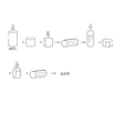
- FIG. 1 is a schematic explanatory diagram for explaining an example of a hot forging step in the method for producing a high-purity copper processed material of the present embodiment.
- a high-purity copper ingot having the above-mentioned unidirectionally solidified structure and a purity of 99.9999% by mass or more is heated to an initial temperature of 550 to 900 ° C. (800 ° C. in FIG. 1) to perform hot forging.
- the hot forging process first, forging is performed in the solidification direction of the high-purity copper ingot. When the thickness becomes 1/2 or less, the ingot is placed horizontally.
- the hot forging step in the present embodiment is preferably hot drawing forging performed at least once in the range of the initial temperature of 550 to 900 ° C.
- the initial temperature of hot forging is less than 550 ° C., the cast structure remains.
- the initial temperature of hot forging is set to 550 to 900 ° C.
- multi-axial drawing forging in which stretching is performed while forging from multiple directions is desirable.
- the reason for water-cooling the hot forging after completion of the hot forging is to prevent the crystal grains of the broken cast structure from growing and coarsening due to the residual heat inside the hot forging. .
- FIG. 2 is a schematic explanatory diagram for explaining an example of a warm forging step in the method for producing a high-purity copper processed material of the present embodiment.
- Warm forging is performed at an initial temperature of 350 to 500 ° C. on the prismatic hot forging material produced by the above hot forging.
- a prismatic hot forging material heated to 420 ° C. is first warm-forged in the axial direction thereof. When the thickness becomes 1/2 or less, the warm forged material is placed horizontally. While rotating this warm forged material, it is struck from its circumferential direction, and multi-axial drawing forging is performed in which it is stretched to a length that is at least twice the original length.
- the prismatic warm forging material is rebuilt and forging is performed again from the axial direction of the prismatic warm forging material.
- the warm forged material is placed again. While turning the warm forged material, it is struck from its circumferential direction, and the multi-axial drawing forging is performed again, which extends to a length that is at least twice the original length. This is repeated, and when the corner of the prismatic warm forging material falls to some extent, tap forging is performed to produce a cylindrical warm forging material. Water cooling is performed before the temperature of the warm forged material falls below 300 ° C.
- a crystal grain structure having an average grain size of about 30 to 80 ⁇ m and a uniform grain size is formed throughout the warm forged material.
- the warm forging temperature range is set to 350 to 500 ° C.
- water cooling before the temperature of the warm forged material falls below 300 ° C. prevents the occurrence of uneven crystal grain growth due to the residual heat of the warm forged material, Moreover, it is for preventing the coarsening of a partial crystal grain.
- cold rolling is performed while rotating at a certain angle, that is, crossing, so that the total reduction ratio is at least 50% or more.
- Perform cold cross rolling.
- the total rolling reduction is less than 50%, the amount of applied strain is small, and static recrystallization may be insufficient.
- cold rolling is performed while crossing.
- the temperature of the copper material is more preferably 85 ° C. or less, and most preferably 70 ° C. or less.
- the high-purity cold-rolled copper material (cold-rolled material) obtained above is subjected to strain relief annealing in a temperature range of 200 to 400 ° C. If the annealing temperature is less than 200 ° C., the processed structure may remain. When the annealing temperature exceeds 400 ° C., the coarsening of crystal grains begins, and the fine crystal structure targeted by this embodiment may not be obtained. Therefore, the strain relief annealing temperature is set to 200 to 400 ° C.
- the high purity copper processed material of the present embodiment is obtained by the above manufacturing method.
- This high-purity copper processed material is made of high-purity copper having a purity of 99.9999% by mass or more, has an average crystal grain size of 20 ⁇ m or less, and 2.5 times the average crystal grain size in the grain size distribution of the crystal grains.
- the area ratio occupied by the crystal grains having a grain size exceeding is less than 10% of the area of all the crystal grains.
- This high-purity copper processed material has a uniform crystal structure throughout and has a fine crystal structure. When the average crystal grain size exceeds 20 ⁇ m, when used as a sputtering target, the effect obtained by the refinement of crystal grains cannot be expected.
- the area ratio of crystal grains having a grain size exceeding 2.5 times the average crystal grain size is 10% or more of the total crystal grain area, the uniformity of the crystal structure becomes insufficient. For this reason, in the sputtering over a long period of time, it becomes impossible to expect the effect obtained by making the crystal grains fine. Therefore, in the present embodiment, the area ratio of crystal grains having an average crystal grain size of 20 ⁇ m or less and having a grain size exceeding 2.5 times the average crystal grain size in the grain size distribution is It is defined as less than 10% of the total crystal grain area.
- a high-purity copper ingot having a Cu purity of 99.9999% by mass or more and a diameter of 250 mm and a length of 600 mm was produced.
- This high-purity copper ingot was produced by unidirectional solidification, and finally the molten metal surface solidified in the production process. For this reason, there were no casting defects such as shrinkage cavities and voids inside the ingot, and the ingot had a sound cast structure.
- As a result of measuring the size of the crystal grain of the ingot it was found that the size of the crystal grain was 1,000 to 200,000 ⁇ m, there were many variations in the crystal grain size, and all the crystal grains were coarse.
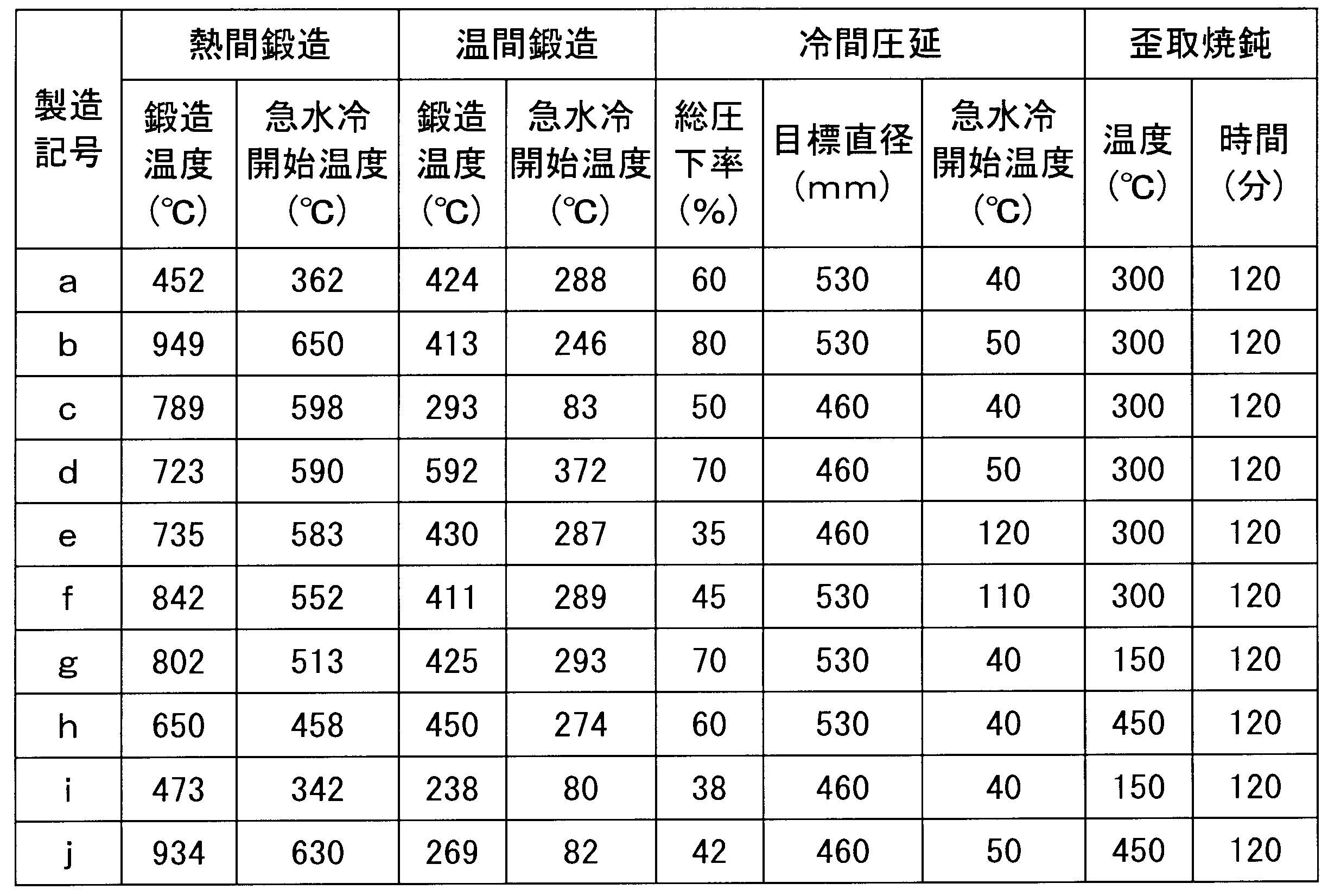
- the high-purity copper ingot was held at the temperature shown in Table 1, and as shown in FIG. 1, first, hot forging was first performed in the solidification direction of the high-purity copper ingot. When the thickness became 1/2 or less, it was placed horizontally. While rotating the ingot, it was struck from its circumferential direction and subjected to multi-axial drawing forging that was extended to a length that was at least twice as long as the original, to obtain a prismatic hot forging material. Subsequently, the prismatic hot forging material was rebuilt, and forging was performed again from the axial direction of the prismatic hot forging material. When the thickness became 1/2 or less, the hot forging was placed again.
- Table 1 shows the temperature of the hot forged material when the rapid water cooling is performed.
- a crystal grain boundary was defined as a measurement point where the orientation difference between adjacent measurement points was 15 ° or more by orientation analysis using the backscattered electron beam analysis method. From the obtained crystal grain boundaries, the number of crystal grains in the observation area was calculated. The crystal grain area was calculated by dividing the total length of the crystal grain boundary in the observation area by the number of crystal grains, and this was converted into a circle to obtain an average crystal grain. (Measurement of crystal grain size variation) From the above measurement, a particle size distribution diagram was created, and the variation was calculated therefrom.
- the high-purity copper processed material having a uniform and fine crystal structure according to this embodiment can be used as an anode for electroplating, for example. In this case, the dissolution is performed more uniformly than in a normal anode. In addition, the black film can be formed uniformly.
- the high-purity copper processed material and the manufacturing method thereof according to one embodiment of the present invention can be suitably applied to a sputtering target manufacturing process for forming a conductive film on a silicon wafer, for example.
Landscapes
- Chemical & Material Sciences (AREA)
- Engineering & Computer Science (AREA)
- Mechanical Engineering (AREA)
- Materials Engineering (AREA)
- Metallurgy (AREA)
- Organic Chemistry (AREA)
- Chemical Kinetics & Catalysis (AREA)
- Physics & Mathematics (AREA)
- Thermal Sciences (AREA)
- Crystallography & Structural Chemistry (AREA)
- Physical Vapour Deposition (AREA)
- Forging (AREA)
Abstract
Description
本願は、2010年3月5日に、日本に出願された特願2010-48516号に基づき優先権を主張し、その内容をここに援用する。
例えば、特許文献1,2に示されたように、微細な結晶粒を有する高純度銅は、以下のように製造される。まず銅を真空又は不活性ガス雰囲気中で溶解・鋳造して純度が99.9999質量%以上の高純度銅インゴットを得る。高純度銅インゴットを550~650℃に加熱し、この加熱された高純度銅インゴットを熱間鍛造し、次いで冷間加工する。次に、初期温度350~500℃の温度範囲内で歪取り焼鈍を行う。冷間加工と歪取り焼鈍を繰り返し行い、最終的に冷間加工する。以上により、高純度銅加工材が得られる。
上記従来技術では、純度:99.9999質量%以上の素材を使用することにより99.9999質量%以上の純度を確保することはできる。しかしながら、平均粒径が200μm以下の微細な結晶粒を工業的に安定して得ることは難しいという問題があった。
例えば、特許文献3では、純度99.9999質量%以上の高純度銅インゴットを300~500℃で熱間鍛造し、次いで冷間加工する。次に歪取り焼鈍を行う。以上により、平均結晶粒径が10~50μmの微細な結晶粒からなり、スパッタリングターゲットや電気めっき用アノードとして用いられる高純度銅加工材を得ている。
また、特許文献4では、高純度銅素材を約-50℃以下の温度に冷却し、次いで加工を施して高純度銅に加工歪みを導入する。次に歪みが導入された高純度銅を約320℃以下の温度で再結晶させる。以上により、約10μm以下の結晶粒度を有する高純度銅加工材を得ている。
特許文献5では、300℃を超える温度で熱間鍛造し、次いで必要により中間焼鈍する。その後、冷間圧延する。以上により、1μm~約50μmの平均結晶粒度を有する高純度銅加工材を得ている。
特許文献6では、熱間鍛造し、次いで水焼入れを行う。その後、冷間圧延する。以上により、比較的均一な結晶粒径を有し、かつ平均結晶粒度が50μm以下の高純度銅加工材を得ている。
例えば、上記特許文献3~6に示される製造方法によれば、結晶粒径が比較的小さい高純度銅が得られる。その結晶粒径の分布を測定した場合、結晶粒径の分布幅が広いことがわかる。特に、純度を高くして、純度:99.9999質量%以上の高純度銅加工材を作製した場合には、結晶粒を均一に微細化することが困難となる。また、仮に平均結晶粒径が小さな数値であっても、粒径のバラツキ幅が大きいため、平均結晶粒径が小さく、かつ加工材全体にわたって結晶粒径が均一である高純度銅加工材は得られていない。
(1)本発明の一態様に係る均一で微細な結晶組織を有する高純度銅加工材は、純度99.9999質量%以上のCuからなり、平均結晶粒径が20μm以下であり、かつ結晶粒の粒径分布において、平均結晶粒径の2.5倍を超える粒径を有する結晶粒が占める面積割合は、全結晶粒の面積の10%未満である。
(2)前記(1)に記載の均一で微細な結晶組織を有する高純度銅加工材では、高純度銅加工材がスパッタリングターゲットであってもよい。
(3)前記(1)または(2)に記載の本発明の一態様に係る均一で微細な結晶組織を有する高純度銅加工材の製造方法は、Cu純度99.9999質量%以上の高純度銅からなる鋳塊を、初期温度550℃以上で熱間鍛造した後水冷し、次いで、初期温度350℃以上で温間鍛造した後水冷し、次いで、50%以上の総圧下率で冷間クロス圧延をし、次いで、200℃以上で歪取焼鈍を行う。
(4)前記(3)に記載の均一で微細な結晶組織を有する高純度銅加工材の製造方法では、前記純度99.9999質量%以上の高純度銅からなる鋳塊として、一方向凝固により製造され、引け巣又はボイドからなる鋳造欠陥が無い高純度銅鋳塊を用いてもよい。
(5)前記(3)または(4)に記載の均一で微細な結晶組織を有する高純度銅加工材の製造方法では、前記熱間鍛造において、初期温度550~900℃の範囲で、熱間圧伸鍛造を少なくとも1回以上行ってもよい。
(6)前記(5)に記載の均一で微細な結晶組織を有する高純度銅加工材の製造方法では、前記熱間圧伸鍛造において、前記鋳塊をその凝固方向に圧縮し、次いで前記鋳塊の凝固方向に垂直な方向であり、かつ少なくとも2軸以上の多方向から前記鋳塊を鍛造しながら、前記鋳塊を伸ばしてもよい。
(7)前記(3)乃至(6)の何れかに記載の均一で微細な結晶組織を有する高純度銅加工材の製造方法では、前記温間鍛造において、初期温度350~500℃の範囲で、温間圧伸鍛造を少なくとも1回以上行ってもよい。
(8)前記(7)に記載の均一で微細な結晶組織を有する高純度銅加工材の製造方法では、前記温間圧伸鍛造において、前記鋳塊をその凝固方向に圧縮後、前記鋳塊の凝固方向に垂直な方向で、かつ、少なくとも2軸以上の多方向から鍛造しながら伸ばしてもよい。
(9)前記(3)乃至(8)の何れかに記載の均一で微細な結晶組織を有する高純度銅加工材の製造方法では、前記歪取り焼鈍を200~400℃の温度範囲で実施してもよい。
本実施形態では、例えば、一方向凝固により銅鋳塊(インゴット)を作製する。溶湯を一方向凝固させると、ガス成分がインゴットの最上面に放出されていく。このため、仮にトラップされたガスが存在していても、表面研削などにより簡単に除去できる。また通常の鋳造法により得られたインゴットよりも、引け巣やボイドの発生が少なく、歩留まりが向上する。
なお、銅鋳塊の製法は、一方向凝固に限定されず、例えば半連続鋳造などによっても、引け巣、ボイド、又は割れなどの鋳造欠陥が無い高純度銅鋳塊を得ることができる。
前述した一方向凝固組織を有し、純度が99.9999質量%以上の高純度銅の鋳塊を、初期温度550~900℃(図1では800℃)に加熱して熱間鍛造を行う。
熱間鍛造工程では、まず、高純度銅鋳塊の凝固方向に鍛造する。その厚さが1/2以下になったとき、鋳塊を横置きする。鋳塊を回しながらその周方向から叩いて、横置きした当初の2倍以上の長さまで伸ばす多軸圧伸鍛造を行い、角柱状の熱間鍛造材とする。次いで、角柱状の熱間鍛造材を立て直して該角柱状の熱間鍛造材の軸方向から再度鍛造を行う。その厚さが1/2以下になったとき、再度熱間鍛造材を横置きする。熱間鍛造材を回しながらその周方向から叩いて、横置きした当初の2倍以上の長さまで伸ばす多軸圧伸鍛造を再度行う。これを繰り返し行うことにより、鋳塊の鋳造組織を破壊する。そして、熱間鍛造の終了後、熱間鍛造材を水冷する。図1においては、8角柱状の熱間鍛造材を得る方法を例示したが、これに限らず、例えば4角柱状の熱間鍛造材を得ることとしてもよい。
作製した鋳塊では、その結晶粒径は、約1000~200000μmという大きな結晶粒径である。しかし、上記熱間鍛造を行うことにより、鋳塊の鋳造組織は破壊され、その結晶粒径は、約80~150μm程度にまで微細化する。
このように、本実施形態における熱間鍛造工程は、初期温度550~900℃の範囲で少なくとも1回以上行う熱間圧伸鍛造であることが好ましい。
ここで、熱間鍛造の初期温度が550℃未満では、鋳造組織が残存してしまう。一方、900℃を超える初期温度で鍛造した場合には、鍛造時の発熱等により、鋳塊の溶融の危険や無駄なエネルギーを使用してしまう。このため、熱間鍛造の初期温度は550~900℃とする。
また、鋳造組織の不均質性(結晶粒径)を解消するためには、多方向から鍛造しながら伸ばしていく多軸圧伸鍛造が望ましい。
さらに、熱間鍛造終了後、熱間鍛造材を水冷するのは、特に、熱間鍛造材内部の残熱によって、破壊した鋳造組織の結晶粒が成長し粗大化するのを防止するためである。
上記の熱間鍛造で作製された角柱状の熱間鍛造材に対して、初期温度350~500℃で温間鍛造を行う。
例えば、420℃に加熱した角柱状の熱間鍛造材に対し、まず、その軸方向に温間鍛造する。その厚さが1/2以下になったとき、温間鍛造材を横置きする。この温間鍛造材を回しながらその周方向から叩いて、横置きした当初の2倍以上の長さまで伸ばす多軸圧伸鍛造を行う。次いで、角柱状の温間鍛造材を立て直して角柱状の温間鍛造材の軸方向から再度鍛造を行う。その厚さが1/2以下になったとき、再度温間鍛造材を横置きする。温間鍛造材を回しながらその周方向から叩いて、横置きした当初の2倍以上の長さまで伸ばす多軸圧伸鍛造を再度行う。これを繰り返し行い、角柱状の温間鍛造材の角がある程度落ちてきた時点でタップ鍛造を行うことによって円柱状の温間鍛造材を作製する。この温間鍛造材の温度が300℃を下回らないうちに水冷する。
上記温間鍛造を施すことにより、平均結晶粒径が約30~80μm程度であって、かつ、温間鍛造材全体にわたって、均一な粒径の結晶粒の組織が形成される。
温間鍛造温度が350℃未満であると、鍛造時に坐屈する危険性が高く、また、加工組織が残存する。一方、温間鍛造温度が500℃を超えると、加工中の組織の粗大化が生じる恐れがある。このため、温間鍛造温度範囲は、350~500℃とする。
また、温間鍛造終了後、温間鍛造材の温度が300℃を下回らないうちに水冷するのは、温間鍛造材の残熱によって、不均一な結晶粒の成長が起こるのを防止し、また、部分的な結晶粒の粗大化を防止するためである。
冷間圧延中は、銅材の温度が100℃を超えないように条件を制御することが好ましい。これにより、歪みの開放を防止でき、再結晶化を抑制できる。なお、銅材の温度は、85℃以下がより好ましく、70℃以下が最も好ましい。
平均結晶粒径が20μmを超えると、スパッタリングターゲットとして用いた場合に、結晶粒が微細化であることにより得られる効果を期待できない。また、平均結晶粒径の2.5倍を超える粒径を有する結晶粒が占める面積割合が、全結晶粒の面積の10%以上である場合、結晶組織の均一性が不十分となる。このため、長期にわたるスパッタリングにおいて、結晶粒が微細化であることにより得られる効果を期待できなくなる。このため、本実施形態では、平均結晶粒径が20μm以下であり、かつ結晶粒の粒径分布において、平均結晶粒径の2.5倍を超える粒径を有する結晶粒が占める面積割合は、全結晶粒の面積の10%未満と定める。
Cu純度が99.9999質量%以上であり、かつ直径:250mm、長さ:600mmの寸法を有する高純度銅鋳塊を製造した。この高純度銅鋳塊は一方向凝固により製造され、製造工程では、最後に溶湯表面が凝固した。このため、鋳塊内部には引け巣やボイド等の鋳造欠陥がなく、鋳塊は健全な鋳造組織を有していた。
鋳塊の結晶粒の大きさを測定した結果、結晶粒の大きさは1000~200000μmであり、結晶粒の大きさのバラツキが多く、かつ、いずれの結晶粒も粗大であることが分かった。
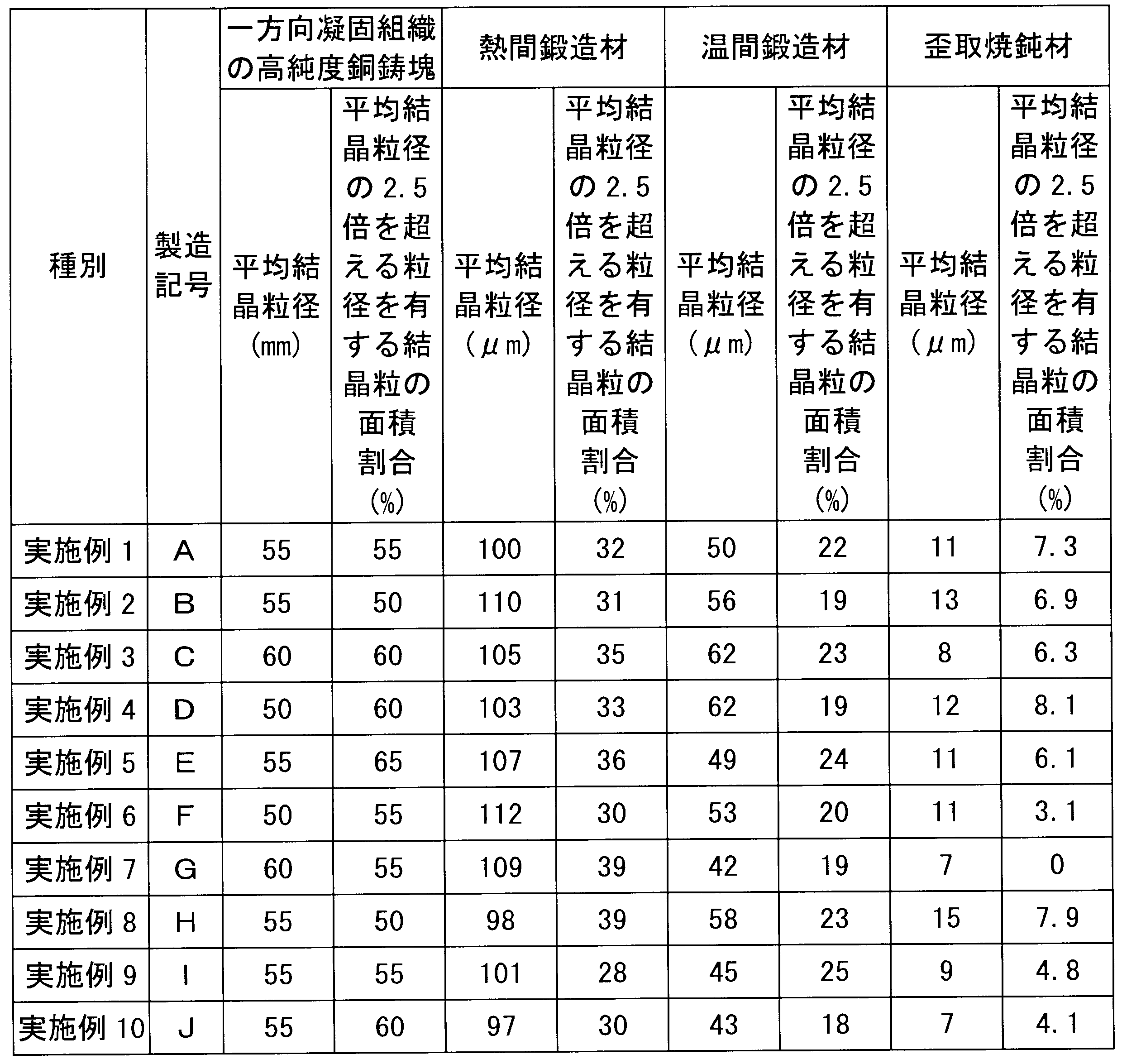
測定した鋳塊の平均結晶粒径、結晶粒径のバラツキ(=平均結晶粒径の2.5倍を超える粒径を有する結晶粒が占める面積割合)を表2に示す。
上記多軸圧伸鍛造を2回行った熱間鍛造材を急水冷した。急水冷を行ったときの熱間鍛造材の温度を表1に示す。
上記熱間鍛造材について測定した平均結晶粒径、結晶粒径のバラツキ(=平均結晶粒径の2.5倍を超える粒径の結晶粒が占める面積割合)を表2に示す。
温間鍛造材の直径が150mmになった時点で温間鍛造を終了し、急水冷した。急水冷を行ったときの温間鍛造材の温度を表1に示す。
上記温間鍛造材について測定した平均結晶粒径、結晶粒径のバラツキ(=平均結晶粒径の2.5倍を超える粒径の結晶粒が占める面積割合)を表2に示す。
上記(A)~(D)の各工程により、表2に示される本実施形態の均一かつ微細な結晶粒を有する高純度銅加工材(実施例という)1~10を製造した。
電界放出型走査電子顕微鏡を用いたEBSD測定装置(HITACHI社製 S4300-SE,EDAX/TSL社製 OIM Data Collection)と、解析ソフト(EDAX/TSL社製 OIM Data Analysis ver.5.2)によって、結晶粒界を特定した。測定条件は測定範囲:680×1020μm/測定ステップ:2.0μm/取込時間:20msec./pointとした。
まず、走査型電子顕微鏡を用いて、試料表面の測定範囲内の個々の測定点(ピクセル)に電子線を照射した。後方散乱電子線解析法による方位解析により、隣接する測定点間の方位差が15°以上となる測定点を結晶粒界とした。
得られた結晶粒界から、観察エリア内の結晶粒子数を算出した。観察エリア内の結晶粒界の全長を結晶粒子数で割って結晶粒子面積を算出し、それを円換算することにより、平均結晶粒とした。
(結晶粒径のバラツキ測定)
上記測定により、粒径分布図を作成し、ここからばらつきを算出した。
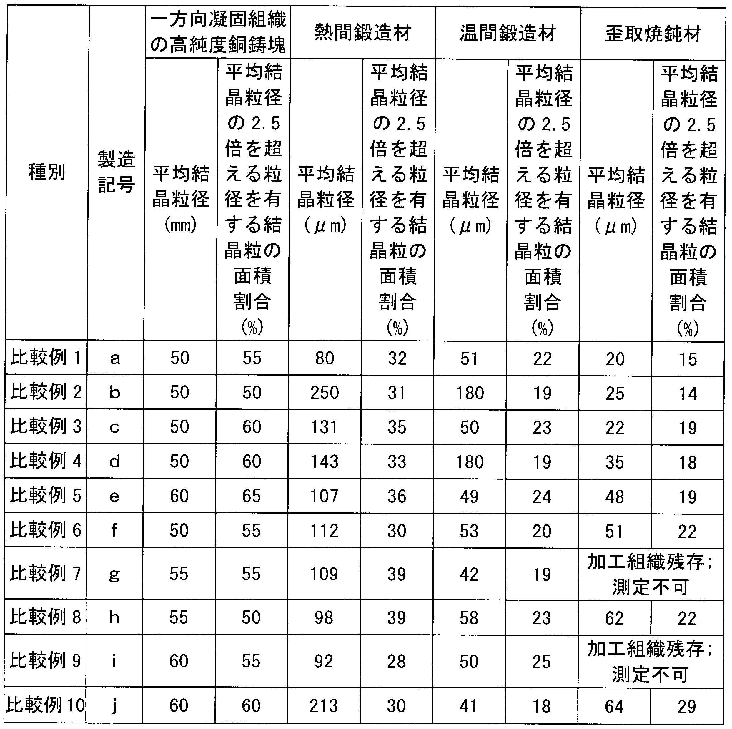
上記で製造した比較例1~10についても、本発明と同様にして、平均結晶粒径、結晶粒径のバラツキ(=平均結晶粒径の2.5倍を超える粒径を有する結晶粒が占める面積割合)を測定した。
この測定値を表4に示す。

その結果を表5に示す。

これに対して、比較例の高純度銅加工材(比較例1~10)から作製したスパッタリングターゲットを用いた場合には、異常放電の発生が見られ、スパッタリングが不安定となった。このため、ウェーハ上に形成されるスパッタ膜に欠陥が発生することを防止できないと考えられる。
Claims (9)
- 純度99.9999質量%以上のCuからなり、
平均結晶粒径が20μm以下であり、かつ結晶粒の粒径分布において、平均結晶粒径の2.5倍を超える粒径を有する結晶粒が占める面積割合は、全結晶粒の面積の10%未満であることを特徴とする均一で微細な結晶組織を有する高純度銅加工材。 - 前記高純度銅加工材がスパッタリングターゲットであることを特徴とする請求項1に記載の均一で微細な結晶組織を有する高純度銅加工材。
- Cu純度99.9999質量%以上の高純度銅からなる鋳塊を、初期温度550℃以上で熱間鍛造した後水冷し、次いで、初期温度350℃以上で温間鍛造した後水冷し、次いで、50%以上の総圧下率で冷間クロス圧延をし、次いで、200℃以上で歪取焼鈍を行うことを特徴とする請求項1に記載の均一で微細な結晶組織を有する高純度銅加工材。
- 前記純度99.9999質量%以上の高純度銅からなる鋳塊として、一方向凝固により製造され、引け巣又はボイドからなる鋳造欠陥が無い高純度銅鋳塊を用いることを特徴とする請求項3に記載の均一で微細な結晶組織を有する高純度銅加工材の製造方法。
- 前記熱間鍛造では、初期温度550~900℃の範囲で、熱間圧伸鍛造を少なくとも1回以上行うことを特徴とする請求項3に記載の均一で微細な結晶組織を有する高純度銅加工材の製造方法。
- 前記熱間圧伸鍛造では、前記鋳塊をその凝固方向に圧縮し、次いで前記鋳塊の凝固方向に垂直な方向であり、かつ少なくとも2軸以上の多方向から前記鋳塊を鍛造しながら、前記鋳塊を伸ばしていくことを特徴とする請求項5に記載の均一で微細な結晶組織を有する高純度銅加工材の製造方法。
- 前記温間鍛造では、初期温度350~500℃の範囲で、温間圧伸鍛造を少なくとも1回以上行うことを特徴とする請求項3に記載の均一で微細な結晶組織を有する高純度銅加工材の製造方法。
- 前記温間圧伸鍛造では、前記鋳塊をその凝固方向に圧縮後、前記鋳塊の凝固方向に垂直な方向で、かつ、少なくとも2軸以上の多方向から鍛造しながら伸ばしていくことを特徴とする請求項7に記載の均一で微細な結晶組織を有する高純度銅加工材の製造方法。
- 前記歪取り焼鈍を200~400℃の温度範囲で実施することを特徴とする請求項3に記載の均一で微細な結晶組織を有する高純度銅加工材の製造方法。
Priority Applications (3)
| Application Number | Priority Date | Filing Date | Title |
|---|---|---|---|
| CN201180009727.0A CN102762757B (zh) | 2010-03-05 | 2011-03-04 | 具有均匀且微细的结晶组织的高纯度铜加工材及其制造方法 |
| KR1020127016631A KR101397857B1 (ko) | 2010-03-05 | 2011-03-04 | 균일하고 미세한 결정 조직을 갖는 고순도 구리 가공재 및 그 제조 방법 |
| US13/580,186 US20120328468A1 (en) | 2010-03-05 | 2011-03-04 | Processed high-purity copper material having uniform and fine crystalline structure, and process for production thereof |
Applications Claiming Priority (2)
| Application Number | Priority Date | Filing Date | Title |
|---|---|---|---|
| JP2010-048516 | 2010-03-05 | ||
| JP2010048516A JP5464352B2 (ja) | 2010-03-05 | 2010-03-05 | 均一かつ微細結晶組織を有する高純度銅加工材の製造方法 |
Publications (1)
| Publication Number | Publication Date |
|---|---|
| WO2011108694A1 true WO2011108694A1 (ja) | 2011-09-09 |
Family
ID=44542339
Family Applications (1)
| Application Number | Title | Priority Date | Filing Date |
|---|---|---|---|
| PCT/JP2011/055039 Ceased WO2011108694A1 (ja) | 2010-03-05 | 2011-03-04 | 均一で微細な結晶組織を有する高純度銅加工材及びその製造方法 |
Country Status (6)
| Country | Link |
|---|---|
| US (1) | US20120328468A1 (ja) |
| JP (1) | JP5464352B2 (ja) |
| KR (1) | KR101397857B1 (ja) |
| CN (1) | CN102762757B (ja) |
| TW (1) | TWI491747B (ja) |
| WO (1) | WO2011108694A1 (ja) |
Cited By (3)
| Publication number | Priority date | Publication date | Assignee | Title |
|---|---|---|---|---|
| CN102534518A (zh) * | 2011-12-29 | 2012-07-04 | 宁波江丰电子材料有限公司 | 背板的制作方法 |
| CN105624622B (zh) * | 2014-11-26 | 2018-02-09 | 宁波江丰电子材料股份有限公司 | 靶材组件的制造方法 |
| CN115341161A (zh) * | 2022-08-22 | 2022-11-15 | 宁波江丰电子材料股份有限公司 | 一种铜铝合金靶材及其制备方法与应用 |
Families Citing this family (16)
| Publication number | Priority date | Publication date | Assignee | Title |
|---|---|---|---|---|
| JP5752736B2 (ja) * | 2013-04-08 | 2015-07-22 | 三菱マテリアル株式会社 | スパッタリング用ターゲット |
| CN104651765A (zh) * | 2013-11-21 | 2015-05-27 | 青岛润鑫伟业科贸有限公司 | 一种由大塑性变形工艺制造的铜片料 |
| CN104694888B (zh) * | 2013-12-09 | 2017-05-10 | 有研亿金新材料股份有限公司 | 一种高纯铜靶材的制备方法 |
| WO2015111563A1 (ja) * | 2014-01-24 | 2015-07-30 | 株式会社フルヤ金属 | 金又は白金ターゲット及びそれらの製造方法 |
| CN107466328A (zh) * | 2015-04-10 | 2017-12-12 | 东曹Smd有限公司 | 钽溅射靶的制造方法和由其制成的溅射靶 |
| US10494712B2 (en) * | 2015-05-21 | 2019-12-03 | Jx Nippon Mining & Metals Corporation | Copper alloy sputtering target and method for manufacturing same |
| EP3342898B1 (en) * | 2015-08-24 | 2023-03-22 | Mitsubishi Materials Corporation | High purity copper sputtering target material |
| CN105887028A (zh) * | 2016-05-13 | 2016-08-24 | 洛阳高新四丰电子材料有限公司 | 一种大尺寸高纯铜平面靶材的制备方法 |
| TWI663274B (zh) | 2017-03-30 | 2019-06-21 | 日商Jx金屬股份有限公司 | Sputtering target and manufacturing method thereof |
| JP7121883B2 (ja) * | 2018-04-09 | 2022-08-19 | 三菱マテリアル株式会社 | スパッタリングターゲット材 |
| KR20210111671A (ko) | 2019-01-07 | 2021-09-13 | 미츠비시 마테리알 가부시키가이샤 | 스퍼터링 타깃재 |
| CN112170753B (zh) * | 2020-08-27 | 2022-05-31 | 金嘉品(昆山)金属工业有限公司 | 一种半导体铜背靶加工方法 |
| CN114000072A (zh) * | 2021-10-28 | 2022-02-01 | 宁波江丰电子材料股份有限公司 | 一种铜背板的热处理方法 |
| CN114210896B (zh) * | 2021-12-23 | 2023-10-03 | 大冶特殊钢有限公司 | 大宽厚比板材的锻造成型方法 |
| CN116351872B (zh) * | 2023-03-03 | 2025-09-16 | 燕山大学 | 借助异步错位轧制实现晶粒细化的方法及其可控ds轧机 |
| CN117107109B (zh) * | 2023-08-30 | 2025-08-15 | 有研工程技术研究院有限公司 | 一种耐高温耐疲劳高强高导铜合金及其制备方法 |
Citations (4)
| Publication number | Priority date | Publication date | Assignee | Title |
|---|---|---|---|---|
| JP2001240949A (ja) * | 2000-02-29 | 2001-09-04 | Mitsubishi Materials Corp | 微細な結晶粒を有する高純度銅加工品素材の製造方法 |
| JP2005533187A (ja) * | 2002-07-16 | 2005-11-04 | ハネウェル・インターナショナル・インコーポレーテッド | 銅スパッタリングターゲット及び銅スパッタリングターゲットの形成方法 |
| JP2007327118A (ja) * | 2006-06-09 | 2007-12-20 | Univ Of Electro-Communications | 金属材料、この金属材料を用いてなるスパッタリングターゲット材、金属材料の微細化加工方法及び装置 |
| JP2009535519A (ja) * | 2006-05-01 | 2009-10-01 | ハネウェル・インターナショナル・インコーポレーテッド | 中空カソードマグネトロンスパッタリングターゲット及び中空カソードマグネトロンスパッタリングターゲットを成形する方法 |
Family Cites Families (9)
| Publication number | Priority date | Publication date | Assignee | Title |
|---|---|---|---|---|
| US6478902B2 (en) * | 1999-07-08 | 2002-11-12 | Praxair S.T. Technology, Inc. | Fabrication and bonding of copper sputter targets |
| US6878250B1 (en) * | 1999-12-16 | 2005-04-12 | Honeywell International Inc. | Sputtering targets formed from cast materials |
| TWI278525B (en) * | 1999-12-16 | 2007-04-11 | Honeywell Int Inc | Copper sputtering targets and methods of forming copper sputtering targets |
| US7090732B2 (en) * | 2000-12-15 | 2006-08-15 | The Furukawa Electric, Co., Ltd. | High-mechanical strength copper alloy |
| JP3861712B2 (ja) * | 2002-02-21 | 2006-12-20 | 石川島播磨重工業株式会社 | Cu基合金、及びこれを用いた高強度高熱伝導性の鍛造物の製造方法 |
| US6896748B2 (en) * | 2002-07-18 | 2005-05-24 | Praxair S.T. Technology, Inc. | Ultrafine-grain-copper-base sputter targets |
| CN1688732B (zh) * | 2002-09-13 | 2010-05-26 | Gbc金属有限责任公司 | 时效硬化型铜基合金及其制备工艺 |
| US20070251818A1 (en) * | 2006-05-01 | 2007-11-01 | Wuwen Yi | Copper physical vapor deposition targets and methods of making copper physical vapor deposition targets |
| WO2010051040A1 (en) * | 2008-11-03 | 2010-05-06 | Tosoh Smd, Inc. | Method of making a sputter target and sputter targets made thereby |
-
2010
- 2010-03-05 JP JP2010048516A patent/JP5464352B2/ja active Active
-
2011
- 2011-03-04 WO PCT/JP2011/055039 patent/WO2011108694A1/ja not_active Ceased
- 2011-03-04 TW TW100107311A patent/TWI491747B/zh active
- 2011-03-04 CN CN201180009727.0A patent/CN102762757B/zh active Active
- 2011-03-04 KR KR1020127016631A patent/KR101397857B1/ko active Active
- 2011-03-04 US US13/580,186 patent/US20120328468A1/en not_active Abandoned
Patent Citations (4)
| Publication number | Priority date | Publication date | Assignee | Title |
|---|---|---|---|---|
| JP2001240949A (ja) * | 2000-02-29 | 2001-09-04 | Mitsubishi Materials Corp | 微細な結晶粒を有する高純度銅加工品素材の製造方法 |
| JP2005533187A (ja) * | 2002-07-16 | 2005-11-04 | ハネウェル・インターナショナル・インコーポレーテッド | 銅スパッタリングターゲット及び銅スパッタリングターゲットの形成方法 |
| JP2009535519A (ja) * | 2006-05-01 | 2009-10-01 | ハネウェル・インターナショナル・インコーポレーテッド | 中空カソードマグネトロンスパッタリングターゲット及び中空カソードマグネトロンスパッタリングターゲットを成形する方法 |
| JP2007327118A (ja) * | 2006-06-09 | 2007-12-20 | Univ Of Electro-Communications | 金属材料、この金属材料を用いてなるスパッタリングターゲット材、金属材料の微細化加工方法及び装置 |
Cited By (4)
| Publication number | Priority date | Publication date | Assignee | Title |
|---|---|---|---|---|
| CN102534518A (zh) * | 2011-12-29 | 2012-07-04 | 宁波江丰电子材料有限公司 | 背板的制作方法 |
| CN105624622B (zh) * | 2014-11-26 | 2018-02-09 | 宁波江丰电子材料股份有限公司 | 靶材组件的制造方法 |
| CN115341161A (zh) * | 2022-08-22 | 2022-11-15 | 宁波江丰电子材料股份有限公司 | 一种铜铝合金靶材及其制备方法与应用 |
| CN115341161B (zh) * | 2022-08-22 | 2023-06-23 | 宁波江丰电子材料股份有限公司 | 一种铜铝合金靶材及其制备方法与应用 |
Also Published As
| Publication number | Publication date |
|---|---|
| CN102762757A (zh) | 2012-10-31 |
| TW201144456A (en) | 2011-12-16 |
| TWI491747B (zh) | 2015-07-11 |
| US20120328468A1 (en) | 2012-12-27 |
| CN102762757B (zh) | 2014-07-09 |
| JP2011184711A (ja) | 2011-09-22 |
| JP5464352B2 (ja) | 2014-04-09 |
| KR20120098819A (ko) | 2012-09-05 |
| KR101397857B1 (ko) | 2014-05-20 |
Similar Documents
| Publication | Publication Date | Title |
|---|---|---|
| JP5464352B2 (ja) | 均一かつ微細結晶組織を有する高純度銅加工材の製造方法 | |
| JP5752736B2 (ja) | スパッタリング用ターゲット | |
| JP4869415B2 (ja) | 純銅板の製造方法及び純銅板 | |
| KR100760156B1 (ko) | 탄탈륨 스퍼터링 타겟트 | |
| JP4976013B2 (ja) | 銅スパッタリングターゲット及び銅スパッタリングターゲットの形成方法 | |
| JP5828350B2 (ja) | 円筒型スパッタリングターゲット用素材の製造方法 | |
| CN108642456B (zh) | Co-Cr-Pt-B型合金溅射靶及其制造方法 | |
| TWI485272B (zh) | Pure copper plate manufacturing methods and pure copper plate | |
| WO2011099426A1 (ja) | 純銅板の製造方法及び純銅板 | |
| JP5668915B2 (ja) | リン成分が均一分散されかつ微細均一な結晶組織を有するめっき用含リン銅アノード材の製造方法およびめっき用含リン銅アノード材 | |
| JP6027823B2 (ja) | 熱延銅板、及び、熱延銅板の形状調整方法 | |
| KR102365363B1 (ko) | 스퍼터링용 티타늄 타깃 및 그 제조 방법, 그리고 티타늄 함유 박막의 제조 방법 |
Legal Events
| Date | Code | Title | Description |
|---|---|---|---|
| WWE | Wipo information: entry into national phase |
Ref document number: 201180009727.0 Country of ref document: CN |
|
| 121 | Ep: the epo has been informed by wipo that ep was designated in this application |
Ref document number: 11750803 Country of ref document: EP Kind code of ref document: A1 |
|
| ENP | Entry into the national phase |
Ref document number: 20127016631 Country of ref document: KR Kind code of ref document: A |
|
| WWE | Wipo information: entry into national phase |
Ref document number: 13580186 Country of ref document: US |
|
| NENP | Non-entry into the national phase |
Ref country code: DE |
|
| 122 | Ep: pct application non-entry in european phase |
Ref document number: 11750803 Country of ref document: EP Kind code of ref document: A1 |