WO2011108663A1 - プラズマエッチング方法、半導体デバイスの製造方法、及びプラズマエッチング装置 - Google Patents
プラズマエッチング方法、半導体デバイスの製造方法、及びプラズマエッチング装置 Download PDFInfo
- Publication number
- WO2011108663A1 WO2011108663A1 PCT/JP2011/054961 JP2011054961W WO2011108663A1 WO 2011108663 A1 WO2011108663 A1 WO 2011108663A1 JP 2011054961 W JP2011054961 W JP 2011054961W WO 2011108663 A1 WO2011108663 A1 WO 2011108663A1
- Authority
- WO
- WIPO (PCT)
- Prior art keywords
- gas
- processing
- processing container
- plasma
- nitride film
- Prior art date
- Legal status (The legal status is an assumption and is not a legal conclusion. Google has not performed a legal analysis and makes no representation as to the accuracy of the status listed.)
- Ceased
Links
Images











Classifications
-
- H—ELECTRICITY
- H10—SEMICONDUCTOR DEVICES; ELECTRIC SOLID-STATE DEVICES NOT OTHERWISE PROVIDED FOR
- H10P—GENERIC PROCESSES OR APPARATUS FOR THE MANUFACTURE OR TREATMENT OF DEVICES COVERED BY CLASS H10
- H10P50/00—Etching of wafers, substrates or parts of devices
- H10P50/20—Dry etching; Plasma etching; Reactive-ion etching
- H10P50/28—Dry etching; Plasma etching; Reactive-ion etching of insulating materials
- H10P50/282—Dry etching; Plasma etching; Reactive-ion etching of insulating materials of inorganic materials
- H10P50/283—Dry etching; Plasma etching; Reactive-ion etching of insulating materials of inorganic materials by chemical means
-
- H—ELECTRICITY
- H10—SEMICONDUCTOR DEVICES; ELECTRIC SOLID-STATE DEVICES NOT OTHERWISE PROVIDED FOR
- H10P—GENERIC PROCESSES OR APPARATUS FOR THE MANUFACTURE OR TREATMENT OF DEVICES COVERED BY CLASS H10
- H10P50/00—Etching of wafers, substrates or parts of devices
- H10P50/20—Dry etching; Plasma etching; Reactive-ion etching
- H10P50/24—Dry etching; Plasma etching; Reactive-ion etching of semiconductor materials
- H10P50/242—Dry etching; Plasma etching; Reactive-ion etching of semiconductor materials of Group IV materials
-
- H—ELECTRICITY
- H01—ELECTRIC ELEMENTS
- H01J—ELECTRIC DISCHARGE TUBES OR DISCHARGE LAMPS
- H01J37/00—Discharge tubes with provision for introducing objects or material to be exposed to the discharge, e.g. for the purpose of examination or processing thereof
- H01J37/32—Gas-filled discharge tubes
- H01J37/32009—Arrangements for generation of plasma specially adapted for examination or treatment of objects, e.g. plasma sources
- H01J37/32192—Microwave generated discharge
-
- H—ELECTRICITY
- H01—ELECTRIC ELEMENTS
- H01J—ELECTRIC DISCHARGE TUBES OR DISCHARGE LAMPS
- H01J37/00—Discharge tubes with provision for introducing objects or material to be exposed to the discharge, e.g. for the purpose of examination or processing thereof
- H01J37/32—Gas-filled discharge tubes
- H01J37/32009—Arrangements for generation of plasma specially adapted for examination or treatment of objects, e.g. plasma sources
- H01J37/32192—Microwave generated discharge
- H01J37/32211—Means for coupling power to the plasma
- H01J37/32238—Windows
-
- H—ELECTRICITY
- H10—SEMICONDUCTOR DEVICES; ELECTRIC SOLID-STATE DEVICES NOT OTHERWISE PROVIDED FOR
- H10D—INORGANIC ELECTRIC SEMICONDUCTOR DEVICES
- H10D30/00—Field-effect transistors [FET]
- H10D30/01—Manufacture or treatment
- H10D30/021—Manufacture or treatment of FETs having insulated gates [IGFET]
- H10D30/0223—Manufacture or treatment of FETs having insulated gates [IGFET] having source and drain regions or source and drain extensions self-aligned to sides of the gate
- H10D30/0227—Manufacture or treatment of FETs having insulated gates [IGFET] having source and drain regions or source and drain extensions self-aligned to sides of the gate having both lightly-doped source and drain extensions and source and drain regions self-aligned to the sides of the gate, e.g. lightly-doped drain [LDD] MOSFET or double-diffused drain [DDD] MOSFET
-
- H—ELECTRICITY
- H10—SEMICONDUCTOR DEVICES; ELECTRIC SOLID-STATE DEVICES NOT OTHERWISE PROVIDED FOR
- H10D—INORGANIC ELECTRIC SEMICONDUCTOR DEVICES
- H10D30/00—Field-effect transistors [FET]
- H10D30/60—Insulated-gate field-effect transistors [IGFET]
- H10D30/601—Insulated-gate field-effect transistors [IGFET] having lightly-doped drain or source extensions, e.g. LDD IGFETs or DDD IGFETs
-
- H—ELECTRICITY
- H10—SEMICONDUCTOR DEVICES; ELECTRIC SOLID-STATE DEVICES NOT OTHERWISE PROVIDED FOR
- H10D—INORGANIC ELECTRIC SEMICONDUCTOR DEVICES
- H10D64/00—Electrodes of devices having potential barriers
- H10D64/01—Manufacture or treatment
- H10D64/015—Manufacture or treatment removing at least parts of gate spacers, e.g. disposable spacers
-
- H—ELECTRICITY
- H10—SEMICONDUCTOR DEVICES; ELECTRIC SOLID-STATE DEVICES NOT OTHERWISE PROVIDED FOR
- H10D—INORGANIC ELECTRIC SEMICONDUCTOR DEVICES
- H10D30/00—Field-effect transistors [FET]
- H10D30/01—Manufacture or treatment
- H10D30/021—Manufacture or treatment of FETs having insulated gates [IGFET]
- H10D30/024—Manufacture or treatment of FETs having insulated gates [IGFET] of fin field-effect transistors [FinFET]
Definitions
- the present invention relates to a plasma etching method using plasma, a semiconductor device manufacturing method, and a plasma etching apparatus.
- Plasma etching technology is an important basic technology along with lithography for forming fine patterns in semiconductor manufacturing.
- the basic mechanism of plasma etching is an ion-assisted etching reaction that occurs due to adsorption of radicals generated by plasma generation onto the film to be etched and ion irradiation by RF. So far, parallel plate, ECR (Electron Cyclotron Resonance), and ICP (Inductively Coupled Plasma) types have been used as plasma sources.
- a silicon nitride film on a silicon substrate or a silicon oxide film may be etched.
- it is required to increase the selectivity of the silicon nitride film with respect to the underlying silicon substrate or silicon oxide film.
- the selection ratio is expressed by the ratio of the etching rate of the silicon nitride film to be etched and the etching rate of the base film not to be etched, and the higher the selection ratio, the better.
- An etching method in which the selection ratio of a silicon nitride film to a silicon substrate or a silicon oxide film is increased is used, for example, in a method for manufacturing a MOS (Metal-Oxide-Semiconductor) transistor.
- MOS Metal-Oxide-Semiconductor
- An example of a method for manufacturing a MOS transistor is as follows.
- FIG. 24 shows an example of a method for manufacturing a MOS transistor.
- MOS transistors As transistors.
- a so-called “shallow junction” in which a pn junction depth is formed shallow is required for the source and drain of the MOS transistor.
- extension regions are formed in the source and drain of the MOS transistor (see, for example, Patent Document 1).
- a silicon oxide film 102 is formed on a silicon substrate 101.
- the polysilicon is patterned by lithography and dry etching to form the gate electrode 103.
- a silicon oxide film 104 is deposited on the substrate by the CVD method. 24C, the silicon oxide film 104 is etched back to form an offset spacer 104a on the side surface of the gate electrode 103, and a gate insulating film 102a is formed under the gate electrode 103. . Subsequently, ion implantation is performed using the gate electrode 103 and the offset spacer 104a as a mask to form extension regions 108 on both sides of the gate electrode 103 in the silicon substrate 101.
- a sidewall spacer 109 made of a silicon oxide film is formed outside the offset spacer 104a.
- ion implantation is performed using the gate electrode 103, the offset spacer 104a, and the sidewall spacer 109 as a mask to form a high concentration source / drain region 107 outside the extension region 108 in the silicon substrate 101.
- the upper surface of the gate electrode 103 and the exposed silicon surface portion of the high-concentration source / drain region 107 are formed.
- a silicide film 110 for reducing resistance is formed in a self-aligned manner on the upper portion of the gate electrode 103 and the exposed surface portion of the high concentration source / drain region 107. .
- miniaturized gate electrode 103 When the miniaturized gate electrode 103 is etched, plasma is generated in the processing container, and RF is applied to a mounting table on which the substrate in the processing container is mounted. Is dry-etched.
- a step of etching the silicon nitride film above the source / drain regions and above the gate electrode 103 is required. There is a case. In this case, etching with an increased selectivity of the silicon nitride film to the underlying silicon substrate or silicon oxide film is required.
- the sidewall spacer 109 is required to have a strength that can withstand ion implantation, a silicon nitride film may be used. Then, in the step shown in FIG. 24E, etching for removing the sidewall spacer 109 made of the silicon nitride film used as a mask at the time of ion implantation is required. That is, it is necessary to perform etching for selectively removing the sidewall spacer 109 made of the silicon nitride film with respect to the offset spacer 104a made of the silicon oxide film.
- an object of the present invention is to increase the selectivity of the silicon nitride film to the underlying silicon substrate or silicon oxide film, thereby preventing the base from being damaged (recessed), and manufacturing a semiconductor device.
- a method and a plasma etching apparatus are provided.
- the first aspect of the present invention is to exhaust the processing gas while supplying the processing gas into the processing container, and set the pressure in the processing container to a predetermined value.
- the silicon nitride film is made to silicon and / or silicon oxide film.
- the processing gas includes a plasma excitation gas, a CHxFy gas, and at least one oxidizing gas selected from the group of O 2 , CO 2 , and CO, with respect to the CHxFy gas.
- the flow rate ratio of the oxidizing gas is set to 4/9 or more when O 2 or CO 2 is used as the oxidizing gas, and CO is used as the oxidizing gas.
- a mixed gas in which at least two of O 2 , CO 2 and CO are used as the oxidizing gas it is converted to O 2 to 4/9 or more.
- It is a plasma etching method characterized by setting.
- X and Y are integers of 1 or more.
- a second aspect of the present invention is a plasma etching method for selectively etching a silicon nitride film, wherein the processing gas is supplied while supplying a processing gas for etching processing into a processing container.
- the pressure in the processing container is set to a pressure of 40.0 Pa or more (300 mTorr or more), and microwaves are introduced into the processing container through a dielectric window on the upper part of the processing container.
- a plasma etching method for selectively etching the silicon nitride film in a non-biased state in which plasma is generated in a container and RF (radio frequency) is not applied to a mounting table on which a substrate in the processing container is mounted. is there.
- X and Y are integers of 1 or more.
- the oxidizing gas is supplied in excess of the amount necessary for removing the CF-based deposit, so that the surface of the silicon substrate is etched while being oxidized.
- a SiO 2 film is formed on the silicon surface. Since there is a relationship of Si—O>Si—N> Si—Si with respect to the binding energy, forming the SiO 2 film on the surface of the silicon substrate hardens the surface of the silicon substrate and lowers the etching rate of silicon. Become.
- the silicon nitride film is also oxidized like the silicon substrate, but the etching rate is not as low as that of silicon, so the selectivity of the silicon nitride film to silicon is increased.
- the etching rate of the silicon oxide film that is originally oxidized is lowered. Therefore, the selectivity of the silicon nitride film to the silicon oxide film is increased.
- the inside of the processing vessel is set to a high pressure of 40.0 Pa or more (300 mTorr or more), and the RF bias applied to the mounting table is set to 0 (no RF bias is applied).
- the ion energy applied to the substrate has a correlation with the sum of the plasma potential energy and the bias applied to the substrate.
- FIG. 1 is an overall configuration diagram of an RLSA etching apparatus according to an embodiment of the present invention.
- a perspective view (including a partial cross-sectional view) showing a slit pattern of RLSA Graph showing the relationship between the distance from the dielectric window and the electron density in the RLSA etching apparatus Graph showing the relationship between the distance from the dielectric window and the electron temperature in the RLSA etching apparatus Process diagram of MOS transistor manufacturing method Cross-sectional view of MOS transistor with side wall spacer isotropically etched Schematic diagram showing damage and footing generated in a silicon substrate ((a) shows damage and (b) shows footing) Process drawing of isotropic etching of sidewall spacer of MOS transistor Process diagram of MOS transistor etching ((a) shows anisotropic etching, (b) shows isotropic etching) Process diagram of FinFET manufacturing method Process diagram of anisotropic etching of semiconductor devices prepared in the example Photograph showing the observation result of recess Photograph showing the observation result of reces
- the plasma etching method of the first and second embodiments of the present invention will be described with reference to the accompanying drawings.
- the plasma etching methods of the first and second embodiments are executed in etching apparatuses having the same structure.
- an RLSA etching apparatus that generates microwave plasma using RLSA (Radial Line Slot Slot Antenna) is used.
- FIG. 1 shows an overall configuration diagram of the RLSA etching apparatus.
- the RLSA etching apparatus uses microwaves as a plasma source. By using the microwave, it is possible to generate a plasma with a low electron temperature and a high density in a region where the etching process is performed.
- the structure of each part of the RLSA etching apparatus is as follows.
- the RLSA etching apparatus includes a cylindrical processing container 1 made of an aluminum alloy or the like.
- the processing container 1 is grounded.
- a mounting table 10 that is erected by a column 9 is provided in the center of the bottom of the processing container 1.
- a semiconductor wafer W is held on the upper surface of the mounting table 10.
- the mounting table 10 is made of a ceramic material such as alumina or alumina nitride.
- the mounting table 10 is embedded with a resistance heater 11 over substantially the entire area thereof, so that the semiconductor wafer W can be heated and maintained at a predetermined temperature.
- the resistance heater 11 is connected to a heater power source 13 through wiring arranged in the support column 9.
- a cooling medium path (not shown) is provided inside the mounting table 10.
- the cooling medium path is formed in an annular shape.
- a thin plate-like electrostatic chuck 14 having conductor wires 12 arranged in a mesh shape inside is provided on the upper surface of the mounting table 10.
- a DC power supply 15 is connected to the conductor wire 12, and the electrostatic chuck 14 electrostatically attracts the semiconductor wafer W placed on the mounting table 10 by a DC voltage supplied from the DC power supply 15.
- a bias high-frequency power source 16 serving as a bias application unit that applies high-frequency power for bias of 13.56 MHz is connected to the conductor wire 12 inside the electrostatic chuck 14 via a matching unit (not shown).
- the matching unit matches the output impedance of the bias high-frequency power supply 16 with the impedance of a load including the mounting table 10, the plasma generated in the processing container 1, and the processing container 1.
- the matching unit includes a blocking capacitor for generating a self-bias.
- the frequency of the high frequency power supplied from the bias high frequency power supply 16 is not limited to 13.56 MHz, but may be a frequency in another RF band such as 27 MHz.
- a plurality of lifting pins 17 are provided for moving the mounting table 10 up and down when the semiconductor wafer W is carried in and out.
- the raising / lowering pin 17 is raised / lowered by the raising / lowering rod 19 provided penetrating the bottom part of the processing container 1 through the bellows 18 which can be expanded and contracted.
- the mounting table 10 is formed with an insertion hole 20 through which the elevating pin 17 can be inserted.
- a loading / unloading port 21 for loading and unloading the semiconductor wafer W is provided in the peripheral wall of the processing container 1.
- the carry-in / out port 21 is provided with a gate valve 22 for opening and closing the carry-in / out port 21 while keeping the inside of the processing container 1 sealed.
- a center gas introduction path 23 for supplying a processing gas into the processing container 1 is provided in the center of the dielectric window 2 on the ceiling of the processing container 1.
- the center gas introduction path 23 is provided so as to penetrate the inner conductor of the coaxial pipe 38.
- an injection port 23a that opens to the processing container is formed in the center of the dielectric window 2a.
- the center gas introduction path 23 is connected to a gas supply source 24 through a gas path 25a.
- a flow rate controller (MFC) for controlling the flow rate of each gas and a valve for turning on and off are provided so that the gas passage 23 can be supplied while controlling the flow rate of each gas of the processing gas. It has become.
- MFC flow rate controller
- the processing gas from the gas supply source 24 flows through the gas passage 25a and the center gas introduction path 23, and is injected toward the mounting table 10 located below from the injection port 23a. Since the processing gas is drawn to the annular exhaust path surrounding the mounting table 10 by the vacuum pump 30, the processing gas sprayed toward the semiconductor wafer W diffuses radially outward in the processing container.
- a gas ring 7 for supplying a processing gas is provided below the injection port 23a and above the semiconductor wafer W.
- the gas ring 7 and the center gas introduction path 23 constitute a processing gas supply unit.
- the gas ring 7 is formed in a hollow ring shape, and has a plurality of side surface outlets at equal intervals in the circumferential direction on the inner peripheral side surface thereof. The plurality of side injection holes are opened in the plasma region in the processing container 1.
- the gas ring 7 is connected to the gas supply source 24 through the gas passage 25b.
- a flow rate controller (MFC) for controlling the flow rate of each processing gas and a valve for turning on and off are provided. The gas ring 7 is controlled while controlling the flow rate of each processing gas.
- the processing gas from the gas supply source 24 is introduced into the gas ring 7 through the gas passage 25b.
- the internal pressure of the gas ring 7 becomes uniform in the circumferential direction when the processing gas is filled, and the processing gas is uniformly injected from a large number of side surface injection ports toward the radially inner region of the gas ring 7 in the processing container 1. Is done. Since the processing gas is supplied from the gas ring 7 to the region where the plasma electron temperature is low (plasma diffusion region), excessive dissociation of the processing gas can be suppressed and an optimal dissociation state can be obtained.
- the processing gas includes plasma excitation gas, CHxFy gas (X and Y are integers of 1 or more), and oxidizing gas.
- the plasma excitation gas includes at least one of Ar, He, Ne, Kr, and Xe.
- CHxFy gas comprises at least one selected from the group consisting of CH 2 F 2, CH 3 F , CHF 2, CHF 3.
- the oxidizing gas includes at least one selected from the group of O 2 , CO 2 , and CO.
- the CHxFy gas and the oxidizing gas constitute the etching gas.
- CHF-based gas radicals are deposited on the substrate to form a deposited film. Oxidizing gases such as O 2 , CO 2 , and CO are used to remove and adjust the carbon component in the deposited film.
- an exhaust port 28 for discharging the processing gas is provided at the bottom of the processing vessel 1.
- a large number of exhaust ports 28 are provided at equal intervals in the circumferential direction.
- an exhaust path 31 Connected to the exhaust port 28 is an exhaust path 31 in which a pressure adjusting valve 29 as a control unit and a vacuum pump 30 as a gas exhaust unit are interposed. Thereby, the pressure in the processing container 1 can be adjusted to a required value.
- a dielectric window 2 is provided on the ceiling of the processing container 1 so as to seal the inside of the processing container 1.
- the dielectric window 2 is made of a dielectric such as quartz, ceramic, alumina (Al 2 O 3 ), or aluminum nitride (AlN), and is permeable to microwaves.
- a convex portion 2 a that protrudes toward the inside of the processing container 1 is formed on the lower surface of the dielectric window 2.
- the configuration of the RLSA 4 that generates microwave plasma is as follows. On the upper surface of the dielectric window 2, an RLSA 4 that generates plasma inside the processing chamber 1 is installed as a microwave introduction unit.
- the RLSA 4 includes a slot plate 3 made of a conductive material and a disk-shaped dielectric plate 5 provided on the upper surface of the slot plate 3.
- the diameter of the slot plate 3 is larger than the diameter of the semiconductor wafer W. For example, when the size of the semiconductor wafer W is 300 mm, the diameter of the slot plate 3 is about 400 to 500 mm.
- the thickness of the slot plate 3 is set to about 1 to several mm.
- the slot plate 3 is made of a copper plate or an aluminum plate whose surface is gold-plated.
- a number of T-shaped slits 3 a that are concentrically distributed are formed in the slot plate 3, and microwaves are radiated into the processing container 1 from the number of slits 3 a.
- the arrangement of the slits 3a is not particularly limited.
- the slits 3a are arranged concentrically, spirally, or radially.
- the dielectric plate 5 provided on the upper surface of the slot plate 3 is made of a dielectric such as quartz, ceramic, alumina (Al 2 O 3 ), or aluminum nitride (AlN).
- the dielectric plate 5 propagates the microwave introduced from the coaxial waveguide 6 in the radial direction and compresses the wavelength of the microwave.
- the upper and lower surfaces of the dielectric plate 5 are covered with a conductor.
- a cooling jacket 8 for cooling the RLSA 4 is provided on the top of the dielectric plate 5.
- the cooling jacket 8 is formed with a flow path connected to a chiller unit (not shown). The cooling jacket 8 absorbs heat generated in the dielectric plate 5 and discharges it to the outside.
- a coaxial waveguide 6 for introducing a microwave is connected to the dielectric plate 5.
- the coaxial waveguide 6 is connected to the microwave generator 34 via the mode converter 32 and the rectangular waveguide 33.
- the microwave generator 34 generates a microwave of 2.45 GHz, for example.
- the frequency of the microwave is not limited to 2.45 GHz, and may be another frequency such as 8.35 GHz.
- the high frequency electric power for generating a microwave is 100 W or more, for example, set to 1500 W, 2000 W, 3000 W, or the like.
- the rectangular waveguide 33 is composed of a rectangular pipe, and propagates microwaves from the microwave generator 34 to the mode converter 32 in the TE mode.
- the mode converter 32 is for connecting the rectangular waveguide 33 to the coaxial waveguide 6, and the TE mode microwave in the rectangular waveguide 33 is converted to the TEM mode microwave in the coaxial waveguide 6. Convert to waves.
- the mode converter 32 is formed in a conical shape that is pointed downward.
- the upper part of the mode converter 32 is coupled to the rectangular waveguide 33, and the lower part of the mode converter 32 is coupled to the inner conductor of the coaxial waveguide 6.
- the coaxial waveguide 6 extends vertically downward from the mode converter 32 toward the RLSA 4 and is connected to the slot plate 3.
- the coaxial waveguide 6 is composed of a double tube having an outer conductor and an inner conductor. The microwave propagates in the TEM mode between the outer conductor and the inner conductor.
- the microwave output from the microwave generator 34 is supplied to the RLSA 4 after passing through the rectangular waveguide 33, the mode converter 32, and the coaxial waveguide 6.
- the microwave is diffused in the radial direction through the dielectric plate 5 of the RLSA 4 and is radiated into the processing container 1 through the slit 3 a of the slot plate 3.
- the processing gas immediately below the dielectric window 2 is ionized, and plasma is generated in the processing container 1.
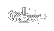
- FIG. 2 shows an example of four slit patterns of RLSA.
- a large number of T-shaped slits 3 a are concentrically arranged in the slot plate 3.
- Each slit 3a is composed of two types of individual slits whose longitudinal directions are orthogonal to each other.
- the pitch in the radial direction of the concentric circles is determined based on the wavelength of the microwave propagating through the RLSA 4 in the radial direction.
- the microwave is converted into a plane wave having two polarization components orthogonal to each other.
- Such an RLSA 4 is effective for uniformly radiating microwaves into the processing container 1 from the entire area of the antenna, and is suitable for generating uniform plasma below the antenna.
- the individual operation and overall operation of the microwave generator 34, the high frequency power supply 16 for bias, the DC power supply 15, the heater power supply 13, the gas supply source 24, the exhaust pump 29, and the like are controlled by the control unit 36.
- the control unit 36 is composed of, for example, a microcomputer.
- a program that defines individual operations and overall operations is stored in a storage medium 37 such as an HDD, a semiconductor memory, or a CD.
- the control unit is provided with a recipe setting unit for setting the flow rate of the processing gas, the pressure in the processing container, the microwave power of the microwave generator 34, and the RF power of the mounting table 10.
- a recipe setting unit for setting the flow rate of the processing gas, the pressure in the processing container, the microwave power of the microwave generator 34, and the RF power of the mounting table 10.
- Various values set in the recipe setting unit are stored in a storage medium 37 such as an HDD, a semiconductor memory, or a CD.
- a feature of the RLSA etching apparatus is that plasma having a low electron temperature and a high density can be generated in the region where the etching process is performed.
- FIG. 3 when microwaves are introduced through the dielectric window 2 at the top of the processing container 1, high-density plasma is excited in a region of 10 to 50 mm immediately below the dielectric window 2.
- FIG. 4 although the plasma in the generation region has a high density and a relatively high electron temperature, the plasma is transported from the generation region to the region where the etching process is performed by diffusion, so that the electron temperature decreases. Since the semiconductor wafer W is placed in a diffusion region having a sufficiently low electron temperature, etching with less ion bombardment damage becomes possible.
- the electron density is attenuated by diffusion, but since the plasma in the generation region is high in density, a sufficiently high density is maintained in the diffusion region.
- the etching method of the first and second embodiments of the present invention is executed using the RLSA etching apparatus having the above configuration.
- the etching methods of the first and second embodiments of the present invention are performed as one step of a semiconductor device manufacturing method.
- a MOS transistor manufacturing method will be described as an example of a semiconductor device manufacturing method.
- FIG. 5 shows a method of manufacturing a MOS transistor in which a “shallow junction” is formed.
- a silicon oxide film 42 as a gate insulating film is formed on the active region of the silicon substrate 41 by thermal oxidation.
- a polysilicon film 43 is deposited on the silicon oxide film 42 by CVD.
- the polysilicon film 43 is patterned by a lithography technique and a dry etching technique to form a gate electrode 44.
- a high-K material may be used for the gate insulating film and a metal may be used for the gate electrode.
- a silicon oxide film 45 is formed on the surface of the gate electrode 44 by, eg, CVD.
- impurity ions are implanted using the gate electrode 44 and the offset spacer 45a as a mask to form extension regions 46 on both sides of the gate electrode 44 in the silicon substrate 41.
- the offset spacer 45a it is possible to shallow the extension region 46 in the silicon substrate 41 directly below the gate electrode 44.
- a silicon nitride film 48 is formed on the silicon substrate 41 by the CVD method, and this is etched back in the step shown in FIG. Is formed on the side surface of the offset spacer 45a. Thereafter, ion implantation of impurity ions is performed using the gate electrode 44, the offset spacer 45a, and the sidewall spacer 48a as a mask, and the high concentration source / drain region 50 is formed outside the extension region 46.
- a cobalt film is deposited on the substrate by the CVD method, the cobalt film and polysilicon are reacted, and then the unreacted metallic cobalt film is removed by etching. Thereafter, by performing phase conversion of the silicide, a silicide film 51 is formed on the gate electrode 44, and a silicide film is also formed on the surface portion of the high concentration source / drain region 50 (not shown).
- the silicon nitride film 48 above the gate electrode 44 and the extension region 46 is formed as shown in FIG. 5 (e) ⁇ FIG. 5 (f). Used for anisotropic etching.
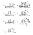
- FIG. 6 shows steps from (e) to (f) in FIG.
- the semiconductor wafer W in which the silicon nitride film 48 is laminated on the silicon substrate 41 is transferred to the RLSA etching apparatus.
- the silicon oxide film 48 is etched back to form sidewall spacers 48a on the side surfaces of the offset spacers 45a.
- the processing gas is exhausted while supplying the processing gas into the processing container 1, and the pressure in the processing container 1 is set to a predetermined value.
- the silicon nitride film 48 is etched by supplying a microwave to generate plasma and setting a bias applied to the mounting table 10 on which the semiconductor wafer W in the processing container 1 is mounted to a predetermined value.
- the processing gas is a gas in which plasma excitation gas, CHxFy gas, and oxidizing gas are mixed.
- the plasma excitation gas includes at least one selected from the group consisting of Ar, He, Ne, Kr, and Xe.
- CHxFy gas comprises at least one selected from the group consisting of CH 2 F 2, CH 3 F , CHF 2, CHF 3.
- the oxidizing gas includes at least one selected from the group of O 2 , CO 2 , and CO.
- the CHxFy gas and the oxidizing gas constitute the etching gas.
- CHF-based gas radicals are deposited on the substrate to form a deposited film. Oxidizing gases such as O 2 , CO 2 , and CO are used to remove and adjust the C content in the deposited film.
- the flow rate ratio of the oxidizing gas to the CHxFy gas is set to O 2 as the oxidizing gas.
- O 2 the oxidizing gas.
- CO 2 the oxidizing gas
- it is set to 4/9 or more
- CO the oxidizing gas
- it is set to 8/9 or more.
- a mixed gas obtained by mixing at least two of O 2 , CO 2 and CO is used as the oxidizing gas, it is set to 4/9 or more in terms of O 2 .
- the flow rate converted to O 2 is ⁇ + ⁇ / 2.
- the flow rate converted to O 2 is ⁇ + ⁇ / 2.
- the flow rate converted to O 2 is ⁇ + ⁇ / 2.
- the flow rate ratio is obtained by dividing the flow rate converted to O 2 by the flow rate of the CHxFy gas.
- the flow rate ratio when converted into O 2 may be set to more than 4/9.
- the flow rate of the oxidizing gas as a scavenger for removing the CF-based deposit is about 1/20 of the flow rate of the CHxFy gas.
- the SiO 2 film is damaged (recessed). For this reason, it is desirable that the thickness of the SiO 2 coating is thin.
- the thickness of the SiO 2 film has a correlation with the ion energy, and the smaller the ion energy, the thinner the SiO 2 film. If the RF bias applied to the mounting table 10 is reduced, the ion energy is reduced. Therefore, when the diameter of the semiconductor wafer W is 300 mm, the RF (less than 30 W / (15 ⁇ 15 ⁇ ⁇ cm 2 ) per 1 cm 2 of wafer ( radio frequency) is applied to the mounting table 10. When the diameter of the semiconductor wafer W is 450 mm, RF of 30 W ⁇ (22.5 ⁇ 22.5 ⁇ ⁇ cm 2 ) / (15 ⁇ 15 ⁇ ⁇ cm 2 ) or less may be applied.
- a footing 48a1 (footing) is formed in the sidewall spacer 48a of the silicon nitride film 48. . If the footing 48a1 is generated, the accuracy of doping in the next process is adversely affected. In order not to generate the footing 48a1 (footing), it is desirable to apply RF (radio frequency) of 20 W / (15 ⁇ 15 ⁇ ⁇ cm 2 ) or more. In the case of etching that does not cause footing, RF may be 20 W or less.
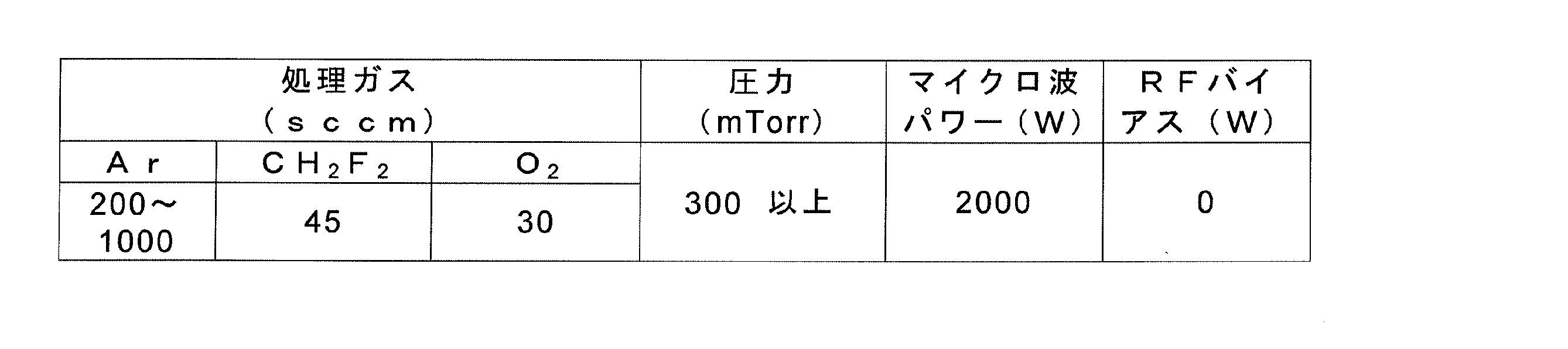
- Table 1 shows an example of the processing conditions of the semiconductor wafer etching method according to the first embodiment of the present invention (when a 300 mm semiconductor wafer W is etched).
- the silicide film 51 is formed on the upper portion of the gate electrode 44 and the surface portion of the source / drain region 50 in the step shown in FIG. It is used in the step of removing the side wall spacer 48a on the side wall of the gate electrode 44 used as a mask.
- the semiconductor wafer W in which the side wall spacer 48a is formed on the gate electrode 44 is transferred to the RLSA etching apparatus.
- the sidewall spacer 48 a on the sidewall of the gate electrode 44 is etched.
- the processing gas is exhausted while supplying the processing gas into the processing container 1, and the pressure in the processing container 1 is set to a predetermined value.
- the silicon nitride film 48 is selectively etched by supplying a microwave to generate plasma and setting a bias applied to the mounting table 10 on which the semiconductor wafer W in the processing chamber 1 is mounted to 0.
- the processing gas is a gas in which plasma excitation gas, CHxFy gas, and oxidizing gas are mixed.
- the plasma excitation gas includes at least one selected from the group consisting of Ar, He, Ne, Kr, and Xe.
- CHxFy gas comprises at least one selected from the group consisting of CH 2 F 2, CH 3 F , CHF 2, CHF 3.
- the oxidizing gas includes at least one selected from the group of O 2 , CO 2 , and CO.
- the CHxFy gas and the oxidizing gas constitute the etching gas.
- CHF-based gas radicals are deposited on the substrate to form a deposited film. Oxidizing gases such as O 2 , CO 2 , and CO are used to remove and adjust the carbon component in the deposited film.
- FIG. 8A shows a state before the removal of the sidewall spacer 48a
- FIG. 8B shows a state after the removal of the sidewall spacer 48a.
- the pressure in the processing chamber 1 where the microwave plasma is generated is 40.0 Pa or more (300 mTorr or more) in order not to damage or recess the underlying silicon oxide film 45 or silicide film 51.
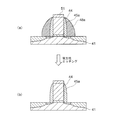
- the sidewall spacer 48a is isotropically etched without applying RF to the mounting table 10. By not applying RF, the ions have no directionality, so that isotropic etching is possible.
- the pressure in the processing container 1 By setting the pressure in the processing container 1 to a high pressure of 40.0 Pa or more (300 mTorr or more), the number of times the ions collide with the gas molecules before reaching the substrate increases, and the directionality tends to be lost. For this reason, isotropic etching becomes possible.
- FIG. 9A shows a comparative example in which RF is applied. When RF is applied, ions are attracted to the silicon substrate 41, and the directionality of ions, that is, anisotropy is generated.
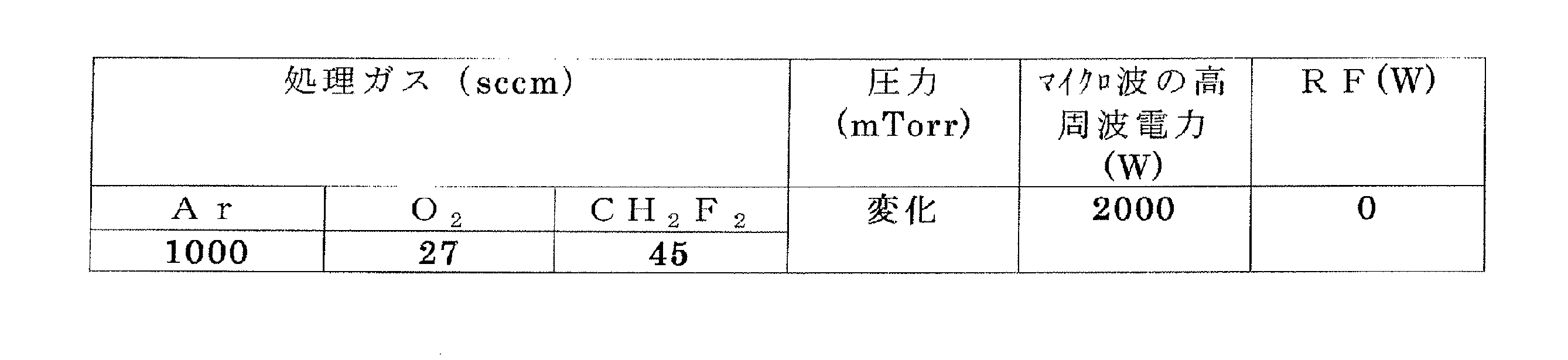
- Table 2 shows an example of the processing conditions of the semiconductor wafer etching method according to the second embodiment of the present invention (when a 300 mm wafer W is etched).
- an RLSA etching apparatus is used to generate plasma.
- a parallel plate, ECR (Electron Cyclotron Resonance), An etching apparatus of ICP (Inductively Coupled Plasma) may be used.
- an RLSA etching apparatus is used to generate plasma.
- plasma can be generated in a processing vessel by microwaves.
- an RLSA etching apparatus can be used.
- another etching apparatus may be used.
- FIG. 10 is a process diagram of a FinFET manufacturing method.
- a silicon region called a fin 62 is formed on the silicon substrate 61, and a silicon oxide film is formed on the upper surface of the fin 62.
- the gate electrode 63 made of polysilicon is etched using the silicon nitride film 65 as a mask. The gate electrode 63 is formed so as to straddle the fin 62, and the side surface of the fin 62 is used as a channel.
- the gate electrode 63 is formed on the silicon substrate 61 via the gate insulating film 64.
- a silicon nitride film 66 is formed on the upper surfaces of the silicon substrate 61, the fins 62, and the silicon nitride film 65 by, for example, the CVD method, and this is a step shown in FIG. Etch back to form a spacer 46 a on the side wall of the gate electrode 63.
- anisotropic etching with an increased selectivity of the silicon nitride film 66 to the silicon substrate and the silicon oxide film is required.
- the semiconductor wafer etching method of the first embodiment of the present invention can be used.
- the spacer 66a on the side wall of the gate electrode 63 needs to be isotropically etched.
- the semiconductor wafer etching method of the second embodiment of the present invention can be used.
- etching methods of the first and second embodiments of the present invention can be applied not only to MOSFET manufacturing methods but also to various semiconductor device manufacturing methods.
- the semiconductor device shown in FIG. 11A was prepared, and the gate electrode 72 made of polysilicon was etched using the silicon nitride film 73 as a hard mask. Next, a 6 nm silicon nitride film 74 was formed on the silicon substrate 71, the gate electrode 72, and the silicon nitride film 73 by CVD. Using the RLSA etching apparatus, the silicon nitride film 74 was anisotropically etched as shown in FIG. Etching process conditions are as follows.
- FIG. 12 shows the observation results of the recess.
- initial indicates a recess before etching
- ME indicates a recess after main etching
- 50% OE indicates a recess after 50% over-etching.
- the number in parentheses in the recess column represents the depth of the recess
- the number with ⁇ represents the amount of increase in the recess after etching. Even when 50% overetching was performed, the amount of increase in the recess was less than 1 nm. The recess value was much lower than that allowed on semiconductor devices. 50% overetching eliminates footing.
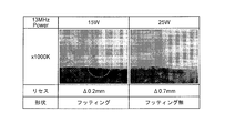
- FIG. 13 shows an observation result of the recess when the RF bias is changed from 15 W to 25 W.
- the RF bias was set to 15 W, footing occurred although the recess was small.
- the RF bias was 25 W, there was no footing. In order to eliminate the footing, it was necessary to set the RF bias to 20 W or more.
- a blanket wafer coated with polysilicon or a silicon nitride film was prepared and etched under various conditions using an RLSA etching apparatus.
- the etching process conditions are as shown in Table 4 below.
- etching rates were measured using an optical interference method, and the dependency of the etching rate on the O 2 flow rate, microwave power, and RF power was examined. Moreover, the surface of the blanket wafer was analyzed using XPS.
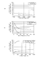
- FIG. 14A shows the O 2 flow rate dependency of the etching rate.
- the selection ratio of the silicon nitride film to silicon increased rapidly.
- the selection ratio became a large value of about 40.
- Increasing the O 2 flow rate decreases both the etching rate of the silicon nitride film and the etching rate of silicon.
- the rate at which the etching rate of silicon decreases is larger than the rate of the silicon nitride film, the etching rate increases.
- the etching rate did not depend on the magnitude of the microwave power or the magnitude of the RF power.
- FIG. 15 shows the results of XPS analysis.
- the surface of the silicon substrate after the etching was analyzed by XPS.
- FIG. 15 shows the results of XPS analysis.
- the O 2 flow rate was increased to 20 sccm or more
- the surface of the silicon substrate was covered with a SiO 2 film. That is, the silicon nitride film is etched while the silicon surface is oxidized to SiO 2 .
- the bond energy has a relationship of Si—O>Si—N> Si—Si.
- the oxide film has a large binding energy and is not easily etched as shown in FIG. Although the binding energy of silicon is small, it is presumed that it becomes difficult to be etched by being oxidized, and this causes a high selection ratio.
- the purpose of adding O 2 gas was to remove carbon (C) in the CF-based deposit. For this reason, the flow rate ratio of O 2 gas to CHxFy gas was set to about 1/20.
- the O 2 gas is supplied in excess to oxidize the silicon surface.
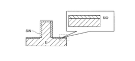
- the relationship between the ion energy and the thickness of the silicon oxide film formed on the silicon surface was examined.
- a silicon oxide film is formed on the surface of the silicon substrate by O 2 gas. This silicon oxide film is counted as a recess.
- the higher the Vpp in other words, the higher the ion energy, the thicker the oxide film. It is considered that the thickness of the silicon oxide film can be reduced if the ion energy is kept low.
- the ion energy has a correlation with the sum of the RF bias voltage Vdc and the plasma potential. As shown in FIG.
- the plasma potential can be reduced compared with the case where the parallel plate etching apparatus is used, so that the ion energy can also be reduced. For this reason, it is considered that the thickness of the oxide film can be reduced.
- an RLSA etching apparatus using RLSA as a plasma source (applicant's RLSA etching apparatus for polyetcher) and an etching apparatus using parallel plates (applicant's parallel plate etching apparatus for polyetcher). ) And the plasma potential were compared.
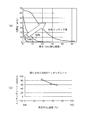
- the ion energy decreased as the pressure in the processing container 1 was increased.
- the ion energy of plasma generated by the RLSA etching apparatus was smaller than that of the parallel plate type etching apparatus.
- the RLSA etching apparatus When viewed at a pressure of 30 mTorr, the RLSA etching apparatus was 7 to 8 eV or less, while the parallel plate etching apparatus was 40 eV.
- the ion energy is proportional to the electron temperature. It has been found that low electron temperature plasma is generated in the RLSA etching apparatus.
- the graph does not show data for RLSA with a pressure of 30 mTorr or higher, but the ion energy continued to decrease even when the pressure was 30 mTorr or higher.
- FIG. 21 (c) shows changes in ion energy when RF is applied to the silicon substrate.
- the ion energy is correlated with the sum of the plasma potential and the RF bias.
- etching can be performed only with the plasma potential.
- etching can be performed with a low ion energy of 7 to 8 eV unless an RF bias is applied.
- high ion energy of about 80 eV remains even if the RF bias is set to zero.
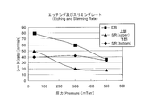
- FIG. 22 shows the etching rate (longitudinal etching rate) and slimming rate (etching rate in the width direction) of the sidewall spacer 48a.
- the slimming rate is measured at two locations, an upper portion and a lower portion of the sidewall spacer 48a.
- the etching rate is increased, the side wall spacer 48a is easily etched in the vertical direction, and when the slimming rate is increased, the side wall spacer 48a is easily etched in the width direction.
- Etching processing conditions processing gas flow rate, pressure, microwave high frequency power, RF bias are as shown in Table 5 below.
- the slimming rate in the width direction of the sidewall spacer 48a hardly changed even when the pressure increased.
- the slimming rate at the lower part of the side wall spacer 48a became a substantially constant value regardless of the pressure, and the slimming rate at the upper part of the side wall spacer 48a became almost constant at 300 mTorr or more.
- the side wall spacer 48a has an etching rate in the vertical direction and a slimming rate in the width direction close to each other, so that isotropic etching is possible.
- the plasma becomes unstable when the pressure is increased to 500 mTorr or more.
- the pressure is preferably set to 500 mTorr or less.
- FIG. 23 shows changes in the etching rates of the silicon nitride film, silicon oxide film, and polysilicon when the pressure is changed.
- the flow rate of O 2 is optimized (specifically, the flow rate of O 2 is 17 to 18 sccm or more).
- the etching rate can be a positive value.
- the etching rate of polysilicon or silicon oxide film is always a negative value of 0 or less regardless of the flow rate of O 2 , that is, a deposited film is formed without being etched. That is, the etching selectivity of the silicon nitride film to the silicon oxide film or polysilicon can be made infinite. Therefore, only the silicon nitride film can be etched without etching the silicon oxide film or the polysilicon.
- the etching rate of the silicon nitride film is an extremely small value, it is possible to control the thickness of the silicon nitride film as thin as about 10 nm. This is particularly effective when the silicon nitride film is left thin without etching the silicon nitride film.
- FIG. 23 shows the etching rates of the silicon nitride film, the silicon oxide film, and the polysilicon when 50 W RF is applied to the silicon substrate.
- the inside of the processing chamber 1 is 40 mTorr, as shown in the upper part of FIG. 23, when the RF bias is 0, the silicon nitride film cannot be etched. However, as shown in the lower part of FIG. 23, when a 50 W RF bias is applied, the silicon nitride film can be etched.
- an RF bias it is estimated that ions enter the silicon nitride film without reacting with the surface of the silicon nitride film and react with the silicon nitride film.
- the etching rate of silicon oxide film and polysilicon is close to 0 even when an RF bias is applied. Therefore, it can be seen that the selection ratio of the silicon nitride film to the silicon oxide film or polysilicon can be increased by applying the RF bias.
- the etching rate of the silicon nitride film can be similarly increased with respect to the silicon oxide film or polysilicon. It was.
- the silicon nitride film 48 is actually etched at an RF of 80 W or less and a pressure of 500 mTorr or less, there are few recesses generated in the silicon oxide film 45 or the gate electrode 44 made of polysilicon, and the shape of the sidewall spacer 48a is also stabilized. I was able to.
Landscapes
- Physics & Mathematics (AREA)
- Engineering & Computer Science (AREA)
- Plasma & Fusion (AREA)
- Chemical & Material Sciences (AREA)
- Analytical Chemistry (AREA)
- Drying Of Semiconductors (AREA)
- Insulated Gate Type Field-Effect Transistor (AREA)
- Electrodes Of Semiconductors (AREA)
- Internal Circuitry In Semiconductor Integrated Circuit Devices (AREA)
- Plasma Technology (AREA)
Abstract
Description



2…誘電体窓
4…RLSA(マイクロ波導入部)
7…シャワーヘッド(処理ガス供給部)
10…載置台
16…バイアス用高周波電源(バイアス印加部)
23…ガス導入管(処理ガス供給部)
29…圧力調整弁
30…真空ポンプ(ガス排気部)
36…制御部
41…シリコン基板(基板)
44…ゲート電極
45…シリコン酸化膜
45a…オフセットスペーサ
48…シリコン窒化膜
49a…スペーサ(サイドウォールスペーサ)
Claims (10)
- 処理容器内に処理ガスを供給しながら前記処理ガスを排気して前記処理容器内の圧力を所定値に設定し、処理ガスに外部エネルギを供給してプラズマを生成し、前記処理容器内の基板が載置される載置台に印加するバイアスを所定値に設定することによって、シリコン窒化膜をシリコン及び/又はシリコン酸化膜に対して選択的にエッチングするプラズマエッチング方法において、
前記処理ガスは、プラズマ励起用ガス、CHxFyガス、並びにO2、CO2、COの群から選ばれる少なくとも一つの酸化性ガスを含み、
前記CHxFyガスに対する前記酸化性ガスの流量比を、前記酸化性ガスとしてO2又はCO2を用いた場合には4/9以上に設定し、前記酸化性ガスとしてCOを用いた場合には8/9以上に設定し、前記酸化性ガスとしてO2、CO2及びCOの少なくとも二つを混合した混合ガスを用いた場合にはO2に換算して4/9以上に設定することを特徴とするプラズマエッチング方法。
ただし、前記CHxFyガスにおいてX及びYは1以上の整数。 - 前記外部エネルギとして、前記処理容器の上部の誘電体窓を介して前記処理容器内にマイクロ波を導入し、
前記処理容器内の基板が載置される載置台に基板1cm2あたり、30W/(15×15×πcm2)以下のRF(radio frequency)を印加することを特徴とする請求項1に記載のプラズマエッチング方法。 - 前記処置容器内の圧力を13.3Pa以下(100mTorr以下)に設定することを特徴とする請求項1又は2に記載のプラズマエッチング方法。
- 前記プラズマエッチング方法は、ゲート電極の側壁にシリコン窒化膜からなるスペーサを形成するためのものであることを特徴とする請求項1ないし3のいずれかに記載のプラズマエッチング方法。
- 処理容器内に処理ガスを供給しながら前記処理ガスを排気して前記処理容器内の圧力を所定値に設定し、処理ガスに外部エネルギを供給してプラズマを生成し、前記処理容器内の基板が載置される載置台に印加するバイアスを所定値に設定することによって、シリコン窒化膜をシリコン及び/又はシリコン酸化膜に対して選択的にエッチングする半導体デバイスの製造方法において、
前記処理ガスは、プラズマ励起用ガス、CHxFyガス、並びにO2、CO2、COの群から選ばれる少なくとも一つの酸化性ガスを含み、
前記酸化性ガスの前記CHxFyガスに対する前記酸化性ガスの流量比を、前記酸化性ガスとしてO2又はCO2を用いた場合には4/9以上に設定し、前記酸化性ガスとしてCOを用いた場合には8/9以上に設定し、前記酸化性ガスとしてO2、CO2及びCOの少なくとも二つを混合した混合ガスを用いた場合にはO2に換算して4/9以上に設定することを特徴とする半導体デバイスの製造方法。
ただし、前記CHxFyガスにおいてX及びYは1以上の整数。 - シリコン窒化膜をシリコン及び/又はシリコン酸化膜に対して選択的にエッチングするプラズマエッチング装置であって、
内部が減圧可能な処理容器と、前記処理容器の内部に設けられる載置台と、前記処理容器に処理ガスを供給する処理ガス供給部と、前記処理容器内の前記処理ガスを排気するガス排気部と、プラズマを生成するために前記処理ガスに外部エネルギを供給するエネルギ供給部と、前記載置台にRF(radio frequency)を印加するバイアス印加部と、前記処理ガスの流量、前記処理容器内の圧力、及び前記載置台に印加されるバイアスを制御する制御部と、を備え、
前記処理ガスは、プラズマ励起用ガス、CHxFyガス、並びにO2、CO2、COの群から選ばれる少なくとも一つの酸化性ガスを含み、
前記制御部は、前記酸化性ガスの前記CHxFyガスに対する前記酸化性ガスの流量比を、前記酸化性ガスとしてO2又はCO2を用いた場合には4/9以上に制御し、前記酸化性ガスとしてCOを用いた場合には8/9以上に制御し、前記酸化性ガスとしてO2、CO2及びCOの少なくとも二つを混合した混合ガスを用いた場合にはO2に換算して4/9以上に制御することを特徴とするプラズマエッチング装置。
ただし、前記CHxFyガスにおいてX及びYは1以上の整数。 - シリコン窒化膜を選択的にエッチングするプラズマエッチング方法であって、
処理容器内にエッチング処理用の処理ガスを供給しながら前記処理ガスを排気して、前記処理容器内の圧力を40.0Pa以上(300mTorr以上)の圧力に設定し、
前記処理容器の上部の誘電体窓を介して前記処理容器にマイクロ波を導入して前記処理容器内にプラズマを発生させ、
前記処理容器内の基板が載置される載置台にRF(radio frequency)を印加しないノンバイアスの状態で、前記シリコン窒化膜を選択的にエッチングするプラズマエッチング方法。 - 前記処理ガスは、
プラズマ励起用ガス、CHxFyガス、並びにO2、CO2、及びCOの群から選ばれる少なくとも一つの酸化性ガスを含むことを特徴とする請求項7に記載のプラズマエッチング方法。
ただし、前記CHxFyガスにおいてX及びYは1以上の整数。 - 前記プラズマエッチング方法は、ゲート電極の側壁のシリコン窒化膜からなるスペーサをエッチングすることを特徴とする請求項7に記載のプラズマエッチング方法。
- シリコン窒化膜を選択的にエッチングするプラズマエッチング装置であって、
内部が減圧可能な処理容器と、前記処理容器の内部に設けられる載置台と、前記処理容器の上部の誘電体窓を介して前記処理容器にマイクロ波を導入するマイクロ波導入部と、前記処理容器に処理ガスを供給する処理ガス供給部と、前記処理容器内の前記処理ガスを排気するガス排気部と、前記処理容器内の圧力を制御する制御部と、を備え、
前記制御部は、前記処理容器内の圧力を40.0Pa以上(300mTorr以上)の圧力に制御し、
前記処理容器内の基板が載置される載置台にRF(radio frequency)を印加しないノンバイアスの状態で、前記シリコン窒化膜を選択的にエッチングするプラズマエッチング装置。
Priority Applications (3)
| Application Number | Priority Date | Filing Date | Title |
|---|---|---|---|
| KR1020127023123A KR101430093B1 (ko) | 2010-03-04 | 2011-03-03 | 플라즈마 에칭 방법, 반도체 디바이스의 제조 방법 및 플라즈마 에칭 장치 |
| US13/582,523 US9324572B2 (en) | 2010-03-04 | 2011-03-03 | Plasma etching method, method for producing semiconductor device, and plasma etching device |
| JP2012503261A JP5466756B2 (ja) | 2010-03-04 | 2011-03-03 | プラズマエッチング方法、半導体デバイスの製造方法、及びプラズマエッチング装置 |
Applications Claiming Priority (2)
| Application Number | Priority Date | Filing Date | Title |
|---|---|---|---|
| JP2010048450 | 2010-03-04 | ||
| JP2010-048450 | 2010-03-04 |
Publications (1)
| Publication Number | Publication Date |
|---|---|
| WO2011108663A1 true WO2011108663A1 (ja) | 2011-09-09 |
Family
ID=44542310
Family Applications (1)
| Application Number | Title | Priority Date | Filing Date |
|---|---|---|---|
| PCT/JP2011/054961 Ceased WO2011108663A1 (ja) | 2010-03-04 | 2011-03-03 | プラズマエッチング方法、半導体デバイスの製造方法、及びプラズマエッチング装置 |
Country Status (5)
| Country | Link |
|---|---|
| US (1) | US9324572B2 (ja) |
| JP (2) | JP5466756B2 (ja) |
| KR (1) | KR101430093B1 (ja) |
| TW (1) | TWI492297B (ja) |
| WO (1) | WO2011108663A1 (ja) |
Cited By (11)
| Publication number | Priority date | Publication date | Assignee | Title |
|---|---|---|---|---|
| WO2013154842A1 (en) * | 2012-04-11 | 2013-10-17 | Tokyo Electron Limited | Aspect ratio dependent deposition to improve gate spacer profile, fin-loss and hardmask-loss for finfet scheme |
| WO2014034229A1 (ja) * | 2012-09-03 | 2014-03-06 | 東京エレクトロン株式会社 | プラズマ処理装置及びこれを備えた基板処理装置 |
| JP2014216331A (ja) * | 2013-04-22 | 2014-11-17 | 株式会社日立ハイテクノロジーズ | プラズマエッチング方法 |
| US8906760B2 (en) | 2012-03-22 | 2014-12-09 | Tokyo Electron Limited | Aspect ratio dependent deposition to improve gate spacer profile, fin-loss and hardmask-loss for FinFET scheme |
| JP2016529736A (ja) * | 2013-08-27 | 2016-09-23 | 東京エレクトロン株式会社 | ハードマスクを横方向にトリミングする方法 |
| JP2017028312A (ja) * | 2016-10-07 | 2017-02-02 | 三菱電機株式会社 | トランジスタの製造方法、増幅器の製造方法 |
| JP2018098480A (ja) * | 2016-12-13 | 2018-06-21 | 東京エレクトロン株式会社 | 窒化シリコンから形成された第1領域を酸化シリコンから形成された第2領域に対して選択的にエッチングする方法 |
| KR101879049B1 (ko) * | 2015-11-30 | 2018-07-16 | 타이완 세미콘덕터 매뉴팩쳐링 컴퍼니 리미티드 | 반도체 구조물 제조 방법 |
| JP2019522889A (ja) * | 2016-06-07 | 2019-08-15 | アプライド マテリアルズ インコーポレイテッドApplied Materials,Incorporated | 高周波結合による高電力静電チャック設計 |
| US11637025B2 (en) | 2016-12-13 | 2023-04-25 | Tokyo Electron Limited | Apparatus for selectively etching first region made of silicon nitride against second region made of silicon oxide |
| WO2026042240A1 (ja) * | 2024-08-22 | 2026-02-26 | 株式会社日立ハイテク | プラズマ処理方法 |
Families Citing this family (36)
| Publication number | Priority date | Publication date | Assignee | Title |
|---|---|---|---|---|
| WO2010004836A1 (ja) * | 2008-07-09 | 2010-01-14 | 東京エレクトロン株式会社 | プラズマ処理装置 |
| US8808561B2 (en) * | 2011-11-15 | 2014-08-19 | Lam Research Coporation | Inert-dominant pulsing in plasma processing systems |
| US9123654B2 (en) * | 2013-02-15 | 2015-09-01 | International Business Machines Corporation | Trilayer SIT process with transfer layer for FINFET patterning |
| JP2015037091A (ja) * | 2013-08-12 | 2015-02-23 | 東京エレクトロン株式会社 | エッチング方法 |
| JP2015050433A (ja) * | 2013-09-04 | 2015-03-16 | 東京エレクトロン株式会社 | プラズマ処理方法 |
| EP2908345A1 (en) | 2014-02-13 | 2015-08-19 | IMEC vzw | Contact formation in Ge-containing semiconductor devices |
| JP6295130B2 (ja) * | 2014-04-22 | 2018-03-14 | 株式会社日立ハイテクノロジーズ | ドライエッチング方法 |
| US10658222B2 (en) | 2015-01-16 | 2020-05-19 | Lam Research Corporation | Moveable edge coupling ring for edge process control during semiconductor wafer processing |
| US9911620B2 (en) * | 2015-02-23 | 2018-03-06 | Lam Research Corporation | Method for achieving ultra-high selectivity while etching silicon nitride |
| KR102354473B1 (ko) | 2015-06-15 | 2022-01-24 | 삼성전자주식회사 | 반도체 소자 및 이의 제조 방법 |
| US9892979B2 (en) | 2015-06-19 | 2018-02-13 | Globalfoundries Inc. | Non-destructive dielectric layer thickness and dopant measuring method |
| US10957561B2 (en) | 2015-07-30 | 2021-03-23 | Lam Research Corporation | Gas delivery system |
| US9837286B2 (en) | 2015-09-04 | 2017-12-05 | Lam Research Corporation | Systems and methods for selectively etching tungsten in a downstream reactor |
| US10192751B2 (en) | 2015-10-15 | 2019-01-29 | Lam Research Corporation | Systems and methods for ultrahigh selective nitride etch |
| US10825659B2 (en) | 2016-01-07 | 2020-11-03 | Lam Research Corporation | Substrate processing chamber including multiple gas injection points and dual injector |
| KR102496037B1 (ko) | 2016-01-20 | 2023-02-06 | 삼성전자주식회사 | 플라즈마 식각 방법 및 장치 |
| US10651015B2 (en) | 2016-02-12 | 2020-05-12 | Lam Research Corporation | Variable depth edge ring for etch uniformity control |
| US10699878B2 (en) | 2016-02-12 | 2020-06-30 | Lam Research Corporation | Chamber member of a plasma source and pedestal with radially outward positioned lift pins for translation of a substrate c-ring |
| US10147588B2 (en) | 2016-02-12 | 2018-12-04 | Lam Research Corporation | System and method for increasing electron density levels in a plasma of a substrate processing system |
| US10438833B2 (en) | 2016-02-16 | 2019-10-08 | Lam Research Corporation | Wafer lift ring system for wafer transfer |
| US10410832B2 (en) | 2016-08-19 | 2019-09-10 | Lam Research Corporation | Control of on-wafer CD uniformity with movable edge ring and gas injection adjustment |
| KR20190038945A (ko) | 2016-08-29 | 2019-04-09 | 도쿄엘렉트론가부시키가이샤 | 실리콘 질화물의 준원자 층 에칭 방법 |
| US10192743B2 (en) | 2016-08-29 | 2019-01-29 | Tokyo Electron Limited | Method of anisotropic extraction of silicon nitride mandrel for fabrication of self-aligned block structures |
| US10431470B2 (en) | 2017-02-23 | 2019-10-01 | Tokyo Electron Limited | Method of quasi-atomic layer etching of silicon nitride |
| US10446405B2 (en) | 2017-02-23 | 2019-10-15 | Tokyo Electron Limited | Method of anisotropic extraction of silicon nitride mandrel for fabrication of self-aligned block structures |
| JP7071850B2 (ja) * | 2017-05-11 | 2022-05-19 | 東京エレクトロン株式会社 | エッチング方法 |
| WO2019103722A1 (en) | 2017-11-21 | 2019-05-31 | Lam Research Corporation | Bottom and middle edge rings |
| KR102003362B1 (ko) | 2017-11-30 | 2019-10-17 | 무진전자 주식회사 | 고 선택적 실리콘 산화물 제거를 위한 건식 세정 장치 및 방법 |
| CN118398464A (zh) | 2018-08-13 | 2024-07-26 | 朗姆研究公司 | 可更换和/或可折叠的用于等离子鞘调整的并入边缘环定位和定心功能的边缘环组件 |
| KR102044763B1 (ko) | 2018-08-22 | 2019-11-15 | 무진전자 주식회사 | 고 선택적 실리콘 산화물 제거를 위한 건식 세정 방법 |
| WO2020093013A1 (en) * | 2018-11-01 | 2020-05-07 | Lam Research Corporation | Method for generating high quality plasma for enhanced atomic layer deposition |
| CN115315775A (zh) | 2020-03-23 | 2022-11-08 | 朗姆研究公司 | 衬底处理系统中的中环腐蚀补偿 |
| JP7409976B2 (ja) * | 2020-06-22 | 2024-01-09 | 東京エレクトロン株式会社 | プラズマ処理システム、プラズマ処理装置及びエッジリングの交換方法 |
| CN116349002A (zh) | 2020-10-05 | 2023-06-27 | 朗姆研究公司 | 用于等离子体处理系统的可移动边缘环 |
| JP7667060B2 (ja) * | 2021-10-22 | 2025-04-22 | 東京エレクトロン株式会社 | プラズマ処理方法及びプラズマ処理システム |
| CN114388359B (zh) * | 2021-12-06 | 2026-01-06 | 信利(惠州)智能显示有限公司 | 过孔干刻的方法 |
Citations (7)
| Publication number | Priority date | Publication date | Assignee | Title |
|---|---|---|---|---|
| WO1998016950A1 (en) * | 1996-10-11 | 1998-04-23 | Tokyo Electron Limited | Plasma etching method |
| JPH11214355A (ja) * | 1998-01-20 | 1999-08-06 | Nec Corp | 異方性ドライエッチング方法 |
| JP2003229418A (ja) * | 2001-11-30 | 2003-08-15 | Tokyo Electron Ltd | エッチング方法 |
| JP2006165030A (ja) * | 2004-12-02 | 2006-06-22 | Ulvac Japan Ltd | トンネル接合素子のエッチング加工方法および装置 |
| JP2008078209A (ja) * | 2006-09-19 | 2008-04-03 | Hitachi High-Technologies Corp | エッチング処理方法 |
| JP2008243942A (ja) * | 2007-03-26 | 2008-10-09 | Renesas Technology Corp | 半導体装置の製造方法及び半導体装置 |
| JP2009026795A (ja) * | 2007-07-17 | 2009-02-05 | Renesas Technology Corp | 半導体装置およびその製造方法 |
Family Cites Families (13)
| Publication number | Priority date | Publication date | Assignee | Title |
|---|---|---|---|---|
| US4412885A (en) * | 1982-11-03 | 1983-11-01 | Applied Materials, Inc. | Materials and methods for plasma etching of aluminum and aluminum alloys |
| JPH06104190A (ja) | 1992-09-17 | 1994-04-15 | Sumitomo Metal Ind Ltd | プラズマプロセス装置 |
| JPH06163471A (ja) * | 1992-11-16 | 1994-06-10 | Nippon Steel Corp | 半導体製造方法 |
| JPH06168920A (ja) | 1992-11-30 | 1994-06-14 | Sumitomo Metal Ind Ltd | 薄膜の除去方法 |
| TW473857B (en) | 1996-04-26 | 2002-01-21 | Hitachi Ltd | Method of manufacturing semiconductor device |
| US6635185B2 (en) * | 1997-12-31 | 2003-10-21 | Alliedsignal Inc. | Method of etching and cleaning using fluorinated carbonyl compounds |
| JP3764594B2 (ja) * | 1998-10-12 | 2006-04-12 | 株式会社日立製作所 | プラズマ処理方法 |
| US6730587B1 (en) * | 2000-12-07 | 2004-05-04 | Advanced Micro Devices, Inc. | Titanium barrier for nickel silicidation of a gate electrode |
| JP2002289841A (ja) | 2001-03-27 | 2002-10-04 | Matsushita Electric Ind Co Ltd | 半導体装置及びその製造方法 |
| KR20030027505A (ko) | 2001-09-28 | 2003-04-07 | 삼성전자주식회사 | 배기 구조가 개선된 반도체 처리장치 |
| US6900104B1 (en) * | 2004-02-27 | 2005-05-31 | Taiwan Semiconductor Manufacturing Co., Ltd. | Method of forming offset spacer manufacturing for critical dimension precision |
| JP2009194032A (ja) * | 2008-02-12 | 2009-08-27 | Tokyo Electron Ltd | プラズマ測定方法及びプラズマ測定装置並びに記憶媒体 |
| JP2009302181A (ja) | 2008-06-11 | 2009-12-24 | Tokyo Electron Ltd | プラズマエッチング処理方法およびプラズマエッチング処理装置 |
-
2011
- 2011-03-03 JP JP2012503261A patent/JP5466756B2/ja not_active Expired - Fee Related
- 2011-03-03 WO PCT/JP2011/054961 patent/WO2011108663A1/ja not_active Ceased
- 2011-03-03 KR KR1020127023123A patent/KR101430093B1/ko not_active Expired - Fee Related
- 2011-03-03 US US13/582,523 patent/US9324572B2/en not_active Expired - Fee Related
- 2011-03-04 TW TW100107394A patent/TWI492297B/zh not_active IP Right Cessation
-
2013
- 2013-10-28 JP JP2013223110A patent/JP5706946B2/ja not_active Expired - Fee Related
Patent Citations (7)
| Publication number | Priority date | Publication date | Assignee | Title |
|---|---|---|---|---|
| WO1998016950A1 (en) * | 1996-10-11 | 1998-04-23 | Tokyo Electron Limited | Plasma etching method |
| JPH11214355A (ja) * | 1998-01-20 | 1999-08-06 | Nec Corp | 異方性ドライエッチング方法 |
| JP2003229418A (ja) * | 2001-11-30 | 2003-08-15 | Tokyo Electron Ltd | エッチング方法 |
| JP2006165030A (ja) * | 2004-12-02 | 2006-06-22 | Ulvac Japan Ltd | トンネル接合素子のエッチング加工方法および装置 |
| JP2008078209A (ja) * | 2006-09-19 | 2008-04-03 | Hitachi High-Technologies Corp | エッチング処理方法 |
| JP2008243942A (ja) * | 2007-03-26 | 2008-10-09 | Renesas Technology Corp | 半導体装置の製造方法及び半導体装置 |
| JP2009026795A (ja) * | 2007-07-17 | 2009-02-05 | Renesas Technology Corp | 半導体装置およびその製造方法 |
Cited By (13)
| Publication number | Priority date | Publication date | Assignee | Title |
|---|---|---|---|---|
| US8906760B2 (en) | 2012-03-22 | 2014-12-09 | Tokyo Electron Limited | Aspect ratio dependent deposition to improve gate spacer profile, fin-loss and hardmask-loss for FinFET scheme |
| WO2013154842A1 (en) * | 2012-04-11 | 2013-10-17 | Tokyo Electron Limited | Aspect ratio dependent deposition to improve gate spacer profile, fin-loss and hardmask-loss for finfet scheme |
| WO2014034229A1 (ja) * | 2012-09-03 | 2014-03-06 | 東京エレクトロン株式会社 | プラズマ処理装置及びこれを備えた基板処理装置 |
| JP2014216331A (ja) * | 2013-04-22 | 2014-11-17 | 株式会社日立ハイテクノロジーズ | プラズマエッチング方法 |
| US9779952B2 (en) | 2013-08-27 | 2017-10-03 | Tokyo Electron Limited | Method for laterally trimming a hardmask |
| JP2016529736A (ja) * | 2013-08-27 | 2016-09-23 | 東京エレクトロン株式会社 | ハードマスクを横方向にトリミングする方法 |
| KR101879049B1 (ko) * | 2015-11-30 | 2018-07-16 | 타이완 세미콘덕터 매뉴팩쳐링 컴퍼니 리미티드 | 반도체 구조물 제조 방법 |
| JP2019522889A (ja) * | 2016-06-07 | 2019-08-15 | アプライド マテリアルズ インコーポレイテッドApplied Materials,Incorporated | 高周波結合による高電力静電チャック設計 |
| JP7101482B2 (ja) | 2016-06-07 | 2022-07-15 | アプライド マテリアルズ インコーポレイテッド | 高周波結合による高電力静電チャック設計 |
| JP2017028312A (ja) * | 2016-10-07 | 2017-02-02 | 三菱電機株式会社 | トランジスタの製造方法、増幅器の製造方法 |
| JP2018098480A (ja) * | 2016-12-13 | 2018-06-21 | 東京エレクトロン株式会社 | 窒化シリコンから形成された第1領域を酸化シリコンから形成された第2領域に対して選択的にエッチングする方法 |
| US11637025B2 (en) | 2016-12-13 | 2023-04-25 | Tokyo Electron Limited | Apparatus for selectively etching first region made of silicon nitride against second region made of silicon oxide |
| WO2026042240A1 (ja) * | 2024-08-22 | 2026-02-26 | 株式会社日立ハイテク | プラズマ処理方法 |
Also Published As
| Publication number | Publication date |
|---|---|
| KR101430093B1 (ko) | 2014-09-22 |
| KR20120120400A (ko) | 2012-11-01 |
| US20130029494A1 (en) | 2013-01-31 |
| JP5466756B2 (ja) | 2014-04-09 |
| TW201201275A (en) | 2012-01-01 |
| TWI492297B (zh) | 2015-07-11 |
| JPWO2011108663A1 (ja) | 2013-06-27 |
| US9324572B2 (en) | 2016-04-26 |
| JP2014060413A (ja) | 2014-04-03 |
| JP5706946B2 (ja) | 2015-04-22 |
Similar Documents
| Publication | Publication Date | Title |
|---|---|---|
| JP5466756B2 (ja) | プラズマエッチング方法、半導体デバイスの製造方法、及びプラズマエッチング装置 | |
| JP5229711B2 (ja) | パターン形成方法、および半導体装置の製造方法 | |
| KR101333352B1 (ko) | 에칭 방법 및 장치 | |
| KR101163276B1 (ko) | 플라즈마 산화 처리 방법 및 플라즈마 처리 장치 | |
| US9263283B2 (en) | Etching method and apparatus | |
| JP2008251855A (ja) | シリコン酸化膜の形成方法 | |
| KR20120069755A (ko) | 선택적 플라즈마 질화 처리방법 및 플라즈마 질화 처리장치 | |
| US20040009634A1 (en) | Method for fabricating a gate structure | |
| JP4906659B2 (ja) | シリコン酸化膜の形成方法 | |
| JP5460011B2 (ja) | 窒化珪素膜の成膜方法、コンピュータ読み取り可能な記憶媒体およびプラズマcvd装置 | |
| KR101028625B1 (ko) | 기판의 질화 처리 방법 및 절연막의 형성 방법 | |
| WO2008041600A1 (en) | Plasma oxidizing method, plasma processing apparatus, and storage medium | |
| CN101151721B (zh) | 绝缘膜的制造方法和等离子体处理装置 | |
| US20060269694A1 (en) | Plasma processing method | |
| JP6424249B2 (ja) | シリコン及びゲルマニウムを含む基板におけるシリコンの優先的酸化のための方法 | |
| JP2009267391A (ja) | 窒化珪素膜の製造方法、窒化珪素膜積層体の製造方法、コンピュータ読み取り可能な記憶媒体およびプラズマcvd装置 | |
| WO2009123325A1 (ja) | 窒化珪素膜の製造方法、窒化珪素膜積層体の製造方法、コンピュータ読み取り可能な記憶媒体およびプラズマcvd装置 |
Legal Events
| Date | Code | Title | Description |
|---|---|---|---|
| 121 | Ep: the epo has been informed by wipo that ep was designated in this application |
Ref document number: 11750772 Country of ref document: EP Kind code of ref document: A1 |
|
| WWE | Wipo information: entry into national phase |
Ref document number: 2012503261 Country of ref document: JP |
|
| ENP | Entry into the national phase |
Ref document number: 20127023123 Country of ref document: KR Kind code of ref document: A |
|
| NENP | Non-entry into the national phase |
Ref country code: DE |
|
| WWE | Wipo information: entry into national phase |
Ref document number: 13582523 Country of ref document: US |
|
| 122 | Ep: pct application non-entry in european phase |
Ref document number: 11750772 Country of ref document: EP Kind code of ref document: A1 |