WO2011108169A1 - インバータ装置及びその制御方法 - Google Patents
インバータ装置及びその制御方法 Download PDFInfo
- Publication number
- WO2011108169A1 WO2011108169A1 PCT/JP2010/072616 JP2010072616W WO2011108169A1 WO 2011108169 A1 WO2011108169 A1 WO 2011108169A1 JP 2010072616 W JP2010072616 W JP 2010072616W WO 2011108169 A1 WO2011108169 A1 WO 2011108169A1
- Authority
- WO
- WIPO (PCT)
- Prior art keywords
- voltage correction
- current
- voltage
- unit
- correction value
- Prior art date
- Legal status (The legal status is an assumption and is not a legal conclusion. Google has not performed a legal analysis and makes no representation as to the accuracy of the status listed.)
- Ceased
Links
Images



Classifications
-
- H—ELECTRICITY
- H02—GENERATION; CONVERSION OR DISTRIBUTION OF ELECTRIC POWER
- H02M—APPARATUS FOR CONVERSION BETWEEN AC AND AC, BETWEEN AC AND DC, OR BETWEEN DC AND DC, AND FOR USE WITH MAINS OR SIMILAR POWER SUPPLY SYSTEMS; CONVERSION OF DC OR AC INPUT POWER INTO SURGE OUTPUT POWER; CONTROL OR REGULATION THEREOF
- H02M7/00—Conversion of AC power input into DC power output; Conversion of DC power input into AC power output
- H02M7/42—Conversion of DC power input into AC power output without possibility of reversal
- H02M7/44—Conversion of DC power input into AC power output without possibility of reversal by static converters
- H02M7/48—Conversion of DC power input into AC power output without possibility of reversal by static converters using discharge tubes with control electrode or semiconductor devices with control electrode
- H02M7/53—Conversion of DC power input into AC power output without possibility of reversal by static converters using discharge tubes with control electrode or semiconductor devices with control electrode using devices of a triode or transistor type requiring continuous application of a control signal
- H02M7/537—Conversion of DC power input into AC power output without possibility of reversal by static converters using discharge tubes with control electrode or semiconductor devices with control electrode using devices of a triode or transistor type requiring continuous application of a control signal using semiconductor devices only, e.g. single switched pulse inverters
- H02M7/5387—Conversion of DC power input into AC power output without possibility of reversal by static converters using discharge tubes with control electrode or semiconductor devices with control electrode using devices of a triode or transistor type requiring continuous application of a control signal using semiconductor devices only, e.g. single switched pulse inverters in a bridge configuration
- H02M7/53871—Conversion of DC power input into AC power output without possibility of reversal by static converters using discharge tubes with control electrode or semiconductor devices with control electrode using devices of a triode or transistor type requiring continuous application of a control signal using semiconductor devices only, e.g. single switched pulse inverters in a bridge configuration with automatic control of output voltage or current
- H02M7/53875—Conversion of DC power input into AC power output without possibility of reversal by static converters using discharge tubes with control electrode or semiconductor devices with control electrode using devices of a triode or transistor type requiring continuous application of a control signal using semiconductor devices only, e.g. single switched pulse inverters in a bridge configuration with automatic control of output voltage or current with analogue control of three-phase output
-
- H—ELECTRICITY
- H02—GENERATION; CONVERSION OR DISTRIBUTION OF ELECTRIC POWER
- H02P—CONTROL OR REGULATION OF ELECTRIC MOTORS, ELECTRIC GENERATORS OR DYNAMO-ELECTRIC CONVERTERS; CONTROLLING TRANSFORMERS, REACTORS OR CHOKE COILS
- H02P21/00—Arrangements or methods for the control of electric machines by vector control, e.g. by control of field orientation
Definitions
- the present invention relates to an inverter device for driving a motor and a control method thereof.
- Patent Document 1 an inverter device capable of outputting a voltage in accordance with a voltage command to a motor is required, and an inverter device in which a deviation voltage due to dead time is not generated has been proposed in order to prevent distortion in the output voltage ( For example, see Patent Document 1).
- the output signal for compensating for the dead time is delayed from the PWM gate signal and input to the gate drive circuit of the transistor so that the transistor as a switching element does not short-circuit the arm.
- the switching delay time is measured every time, and even if the ON switching time, OFF switching time, and dead time of the transistor change, the control amount is made variable.
- the PWM gate signal and the output voltage signal are always delayed by a certain time.
- the conventional inverter device requires a voltage detection circuit for obtaining an output voltage signal. Furthermore, the deviation voltage is suppressed to 2 ⁇ (td-tS) period (td: dead time, tS: storage time) every half cycle of the fundamental frequency, but the semiconductor characteristics and drive of the transistors and diodes constituting the switching element There is no suppression effect on the compensation of the voltage generated by the stray capacitance of the circuit.
- the present invention has been made in view of such problems, and provides an inverter device that can eliminate a voltage detection circuit and can compensate for voltage errors caused by factors other than dead time, and a control method therefor. For the purpose.
- a typical invention of the present application is an inverter device including a power unit that performs PWM control of a voltage command to a motor for each set time period and outputs AC power, and is N times the time period (N ⁇ 1).
- a voltage command generation unit that generates a voltage command in synchronization with a cycle of the period, a section determination unit that generates a section determination signal that turns on a half cycle of the time period, and turns off a next half cycle; and At the change timing, the voltage command is corrected so that the amount of change in current detection when the section determination signal is on is equal to the amount of change in current detection when off.
- Another representative invention of the present application is a control method of an inverter device including a power unit that performs PWM control of a voltage command to a motor for each set time period, converts DC power to AC power, and outputs the power.
- a voltage command is generated in synchronization with a period N times (N ⁇ 1) of the time period, and a section determination signal is generated that turns on the half cycle of the time period and turns off the next half period.
- a difference value between the current detection value detected at the signal change timing and the previous value is calculated, and a voltage correction value at which the current change amount at the time of turning on the section determination signal is equal to the current change amount at the off time is calculated as the motor.
- the current ripple component is reduced by equalizing the magnitude of the current ripple component in the first half period and the second half period of the PWM control, so that the vibration of the same period as the PWM control period and the noise caused by the same are suppressed. it can.
- the block diagram of the inverter apparatus which shows 1st Example of this invention.
- generation part 12 of this invention Test data showing the effect of the present invention
- the block diagram of the inverter apparatus (at the time of table creation) which shows 2nd Example of this invention
- the block diagram of the inverter apparatus (at the time of table reading) which shows 2nd Example of this invention
- the flowchart which shows the process sequence in the voltage correction table preparation part 30 of this invention.
- the power unit for power conversion includes a transistor Tr and a diode FD connected in reverse parallel thereto for each phase.
- the semiconductor characteristics of the diode that constitutes this transistor Tr are such that if the current flowing through the motor is small, the diode FD connected in reverse parallel to the transistor Tr will not turn on completely, causing delay in switching of the transistor Tr, There is a tendency to become a halfway voltage level without being switched.
- Such a switching delay of the transistor Tr differs depending on the on timing and the off timing of the gate signal for base driving the transistor Tr.
- a similar problem occurs due to the influence of stray capacitance around the main circuit. For example, the effect of a floating capacitor between the emitter and collector of the transistor Tr. Depending on the magnitude of the current flowing through the motor, a difference occurs in the time for which the floating capacitor is charged. When the floating capacitor is charged, the current is zero when the minute current command is used. Due to these influences, the motor terminal voltage becomes a halfway voltage level. Even with factors other than the dead time, a voltage error occurs due to such a phenomenon. This voltage error becomes a different value between the first half period and the second half period of the PWM control period, and a current ripple occurs.
- the ripple component of the motor current is extracted for each of the first half cycle and the second half cycle in the PWM control cycle, and the difference between the current ripple components generated in the first half cycle and the second half cycle is zero.
- the voltage error is corrected using the output as a voltage correction value.
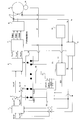
- FIG. 1 is a block diagram of an inverter device showing a first embodiment of the present invention.
- This inverter device includes a current control unit 1, subtracters 2 and 3, a coordinate conversion unit 4, a current detector 5, a coordinate conversion unit 6, a PWM signal generation unit 7, a power unit 8, a motor 9, and a PWM periodic signal generation unit 10.
- the current control unit 1 generates Vd_ref1 and Vq_ref1 by performing, for example, PI (proportional / integral) control individually for Id and Iq so that given current commands Id_ref and Iq_ref coincide with detection currents Id and Iq described later.
- d and q indicate components in a coordinate system in which the d axis that is the magnetic pole position direction and the q axis that is orthogonal to the d axis are used.
- the subtractors 2 and 3 subtract voltage correction values Vdfc and Vqfc, which will be described later, from Vd_ref1 and Vq_ref1, respectively, and output dq voltage commands Vd_ref and Vq_ref.
- the coordinate conversion unit 4 outputs the phase voltage commands Vu_ref, Vv_ref, Vw_ref obtained by dq / UVW coordinate conversion using the dq voltage commands Vd_ref, Vq_ref and the magnetic flux phase ⁇ .
- the magnetic flux phase ⁇ is detected by the magnetic pole phase detector 14 to which the motor shaft of the motor 9 is attached.
- the current detector 5 detects the phase currents Iu, Iv, and Iw of the motor 9 every half cycle of the set cycle in synchronization with an interval determination signal SD described later.
- the coordinate conversion unit 6 converts the phase currents Iu, Iv, and Iw into detection currents Id and Iq by the inverse operation of the coordinate conversion unit 4.
- the PWM signal generator 7 converts the phase voltage commands Vu_ref, Vv_ref, Vw_ref into PWM pulses by performing PWM (pulse width modulation) control using a PWM control signal described later, for example, a triangular wave carrier wave, and gate signals PWMU, PWMV, Outputs PWMW.
- the power unit 8 includes a main circuit including a transistor Tr and a flywheel diode FD for each phase and each upper and lower arm, and a base drive circuit for the transistor Tr, and voltages according to phase voltage commands Vu_ref, Vv_ref, and Vw_ref according to the gate signal. Is output to drive the motor 9.
- the PWM periodic signal generator 10 outputs a triangular wave carrier wave as a PWM periodic signal.
- the triangular carrier wave may have another shape such as a sawtooth wave.
- the section determination unit 11 outputs a section determination signal SD that turns off (0) the count-up section (first half cycle) of the triangular wave carrier wave, which is a PWM periodic signal, and turns on (1) the countdown section (second half cycle).
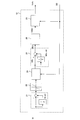
- the d-axis voltage correction value generation unit 12 includes a subtractor 21, a dead zone 22, a sign inverter 24, an adder 25, a controller 26, and a sign inverter 28.
- the subtractor 21 calculates a difference ⁇ Id between the detected current Id and the previous value Id_old.
- the dead zone unit 22 performs dead zone processing on the difference ⁇ Id.
- the dead zone 22 is provided as needed mainly for the purpose of removing quantization errors and switching noise during current detection.
- the sign inverter 24 sets the difference ⁇ Id to Idfc if the section determination signal SD is off (0), and inverts the sign of the difference ⁇ I to set it to Idfc if the section determination signal SD is on (1).
- the adder 25 adds Idfc and the previous value Idfc_old to obtain Idfc1, and updates the previous value Idfc_old to Idfc. In this way, the ripple component of the detection current Id is extracted every half cycle of the triangular wave carrier wave, and the difference between the current ripple components generated in the first half cycle and the second half cycle is extracted as Idfc1.
- the controller 26 performs control so that the current ripple component difference Idfc1 becomes zero, and calculates the d-axis voltage correction value Vdfc1.
- the controller 26 includes at least a controller using a proportional or integrator.
- the sign inverter 28 sets the d-axis voltage correction value Vdfc to Vdfc if the section determination signal SD is off (0), and inverts the sign of the d-axis voltage correction value Vdfc if the section determination signal SD is on (1). To Vdfc. In this way, the d-axis voltage correction value Vdfc that compensates for the difference between the current ripple components is generated.
- the d-axis voltage correction value generation unit 12 outputs the d-axis voltage correction value Vdfc to the subtracter 2 shown in FIG.
- the q-axis voltage correction value generation unit 13 performs the same processing as the d-axis voltage correction value generation unit 12 on the detected current Iq to generate a q-axis voltage correction value Vqfc, and outputs it to the subtracter 3 shown in FIG. To do. Thus, Example 1 is performed.
- the difference between the current ripple components generated in the first half cycle and the second half cycle of the triangular wave carrier wave may constitute an FFT by software, and a frequency component corresponding to one cycle of the triangular wave carrier wave may be extracted.
- a dead time circuit is added to the normal PWM signal generator 7. Voltage compensation for this is performed by adding a voltage drop value corresponding to the dead time Td time to the dq voltage commands Vd_ref, Vq_ref or phase voltage commands Vu_ref, Vv_ref, Vw_ref in the coordinate conversion unit 4 or in the PWM signal generation unit 7.
- the dead time Td is corrected in advance to the pulse width of the PWM pulse.
- the magnetic flux phase ⁇ has been described as being detected using the magnetic pole phase detector 14. However, the magnetic flux phase ⁇ is determined using a magnetic pole estimator that receives the command current or detection current of the motor 9, the command voltage, or the detection voltage. It may be obtained by estimation.
- FIG. 3 is test data showing the effect of the present invention, and is a result of FFT analysis of sound generated from the motor 9.
- FIG. 3A is a power spectrum diagram to which Example 1 is not applied
- FIG. 3B is an applied power spectrum diagram.
- the capacity of the motor used in the test is 200 [W]
- the rated current is 1.2 [Arms]
- the period of the triangular wave carrier is 250 [ ⁇ s]
- the motor is in a rotation stop state
- the current is about 8 of the rated current. [%] Equivalent value.
- the power spectrum value at the frequency of 4 kHz of the triangular wave carrier wave is greatly reduced by applying the first embodiment.
- vibration in the PWM control cycle can be reduced, and noise associated therewith can be reduced.
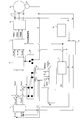
- FIGS. 4 and 5 are block diagrams of an inverter device showing a second embodiment of the present invention.
- the inverter device additionally includes an operation mode switching unit 32 and a voltage correction value reading unit 33 from the configuration of FIG. 1, and a voltage correction table is used instead of the d-axis voltage correction value generation unit 12 and the q-axis voltage correction value generation unit 13.
- a creation unit 30 and a voltage correction value storage unit 31 are provided.
- the second embodiment will be described focusing on the creation and reading of the voltage correction table.
- the voltage correction table is created with the configuration shown in FIG.
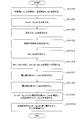
- the voltage correction table creation unit 30 creates a voltage correction table by the sequence processing shown in FIG. This creation process will be described.
- the magnetic flux phase ⁇ used in the coordinate conversion unit 4 and the coordinate conversion unit 6 is switched to the electrical angle phase ⁇ i of the current by an operation mode switching unit 32 described later.
- the electrical angle phase ⁇ i is set to 0 [deg]
- the current commands Id_ref and Iq_ref are set to 0, and the current control unit 1 is set to start the operation.
- the magnitude of the ripple of the detection current Id is compared between the first half cycle and the second half cycle for each half cycle of the triangular wave carrier wave, and the voltage correction value Vdfc1 is increased or decreased so as to match.
- the voltage correction table creation unit 30 inverts the sign of the voltage correction value Vdfc1 being adjusted as it is when the section determination signal SD is off (0), and when it is on (1), to the subtracter 2.
- the d-axis voltage command Vd_ref is generated by subtracting it from Vd_ref1 output by the current control unit 1.
- the above process is repeated to determine the voltage correction value Vdfc1 when the magnitude of the ripple of the detected current Id matches in the first half cycle and the second half cycle for every half cycle of the triangular wave carrier wave.
- the coincidence condition at this time is (A + B) / 2 when the above difference falls within a predetermined value or when the voltage correction value Vdfc1 repeats with values of A and B. Good.
- the processing so far is also performed for the detection current Iq, and the voltage correction value Vqfc1 is determined by repeating until the magnitude of the ripple of the detection current Iq matches every half cycle of the triangular wave carrier wave.
- the electrical angle phase ⁇ i (i) of the current at this time Idref is the current magnitude Iref (j), the determined voltage correction value Vdfc1 is Vdfc2 (i, j), and Vqfc1 is Vqfc2 (i, j) To the voltage correction value storage unit 31.
- the above processing is performed for each Istep from 0 to Iend for the electrical angle phase ⁇ i, and for each Jstep from 0 to Jend for the current command Id_ref for the electrical angle phase ⁇ i.
- the voltage correction table creation unit 30 generates a voltage correction table, and the voltage correction value storage unit 31 uses the electrical angle phase ⁇ i (i) and the current magnitude Iref (j) as arguments.
- a voltage correction table of values Vdfc2 (i, j) and Vqfc2 (i, j) is stored internally.
- the values of Istep and Jstep are basically determined according to the required accuracy and the allowable table size (memory capacity). Note that since the rate of change of the voltage correction value is larger in the region where the current command Id_ref is smaller, the variable amount of the current magnitude is not constant, and an efficient table can be created by changing the smaller the smaller. Further, if the maximum value of the voltage correction value and the maximum value of the electrical angle phase ⁇ i necessary for the table are known in advance, the table may be created based on the size.
- the characteristics of the transistors Tr and the like may be the same for each phase and each upper and lower arm, and the electrical angle phase ⁇ i may be a table in the range of 0 to 60 degrees.
- the operation mode switching unit 32 stores a voltage correction table of voltage correction values Vdfc2 (i, j) and Vqfc2 (i, j) in the voltage correction value storage unit 31 (table creation mode), and a voltage correction value storage unit
- the mode (table reading mode) for reading voltage correction values Vdfc2 (i, j) and Vqfc2 (i, j) from 31 is switched.
- the switching of the operation is performed by switching the voltage correction values Vdfc and Vqfc and the magnetic flux phase ⁇ to the subtracters 2 and 3 and the current commands Id_ref and Iq_ref (not shown).
- the voltage correction value Vdfc1Vqfc1 output from the voltage correction value storage unit 31, the electrical angle phase ⁇ i, and the current command that is sequentially changed.
- the voltage correction values Vdfc2 and Vqfc2 output from the voltage reading unit 33, the magnetic flux phase ⁇ output from the magnetic pole phase detector 14, and the current command given from the outside.
- the voltage correction value reading unit 33 uses the electrical angle phase ⁇ i (i) and the magnitude Iref (j) of the current as arguments from the voltage correction table stored in the voltage correction value storage unit 31 in the table reading mode.
- the voltage correction values Vdfc2 (i, j) and Vqfc2 (i, j) are read as values corresponding to.
- the electrical angle phase ⁇ i (i) and the magnitude Iref (j) of the current are obtained as equations (1) and (2), respectively, and the values before and after the corresponding values from the table created in the voltage correction value storage unit 31. Are linearly interpolated to obtain voltage correction values Vdfc2 and Vqfc2.
- the voltage correction table may be created as a table of the phase voltage in the UVW, and the voltage correction table may be at least the electrical angle phase ⁇ i or the magnitude of the current. It may be created as one function of Iref.
- the voltage correction values Vdfc2 and Vqfc2 may be converted to two-phase / three-phase, or the voltage correction values may be corrected to U, V, and W phase voltage commands.
- the voltage correction values Vufc2 (i, j), Vvfc2 (i, j), and Vwfc2 (i, j) may be measured.
- voltage correction values for two phases for example, Vufc2 (i, j) and Vwfc2 (i, j) are measured, and the voltage correction value for the remaining one phase is calculated from the measured voltage correction values for two phases. A value may be calculated.
- the voltage correction value for one phase may be measured using the fact that the voltage output of the remaining two phases changes when the voltage command is corrected for one phase, and the voltage correction value may be used for correction. At this time, the voltage command for one phase may be selected from among the three phases.
- FIG. 7 is a flowchart illustrating a method for controlling the inverter device according to the third embodiment. Each step will be described in turn.
- step ST1 the phase currents Iu, Iv, Iw of the motor 9 are detected at the timings of the peaks and troughs of the triangular wave carrier wave, and are converted into detected currents Id, Iq.
- step ST2 Vd_ref1 and Vq_ref1 are generated by performing, for example, PI (proportional / integral) control so that the given current commands Id_ref and Iq_ref coincide with the detected currents Id and Iq.
- PI proportional / integral
- step ST3 differences ⁇ Id and ⁇ Iq between the detected currents Id and Iq and their previous values are calculated.
- step ST4 a section discrimination signal SD is generated that turns off the change section from the valley to the peak of the triangular wave carrier wave (0) and turns on the change section from the peak to the valley (1).
- step ST5 if the section discrimination signal SD is off (0), ⁇ Id is set to Idfc and ⁇ Iq is set to Iqfc. If the section discrimination signal SD is on (1), ⁇ Id is set to Idfc and ⁇ Iq is set to Iqfc. In step ST6, Idfc and Iqfc are respectively added to the previous values Idfc_old and Iqfc_old to obtain Idfc1 and Iqfc1, and the previous values Idfc_old are updated by Idfc and Iqfc_old are saved by Iqfc.
- step ST7 for example, PI control is performed so that Idfc and Iqfc become zero, and the outputs are set as voltage correction values Vdfc1 and Vqfc1, respectively. If the section determination signal SD is off (0) in step ST8, Vdfc1 and Vqfc1 are set as voltage correction values Vdfc and Vqfc. If the section discrimination signal SD is ON (1), ⁇ Vdfc1 and ⁇ Vqfc1 are set as voltage correction values Vdfc and Vqfc.
- step ST9 the voltage correction values Vdfc and Vqfc are subtracted from Vd_ref1 and Vq_ref1 to generate dq voltage commands Vd_ref and Vq_ref.
- step ST10 voltage is output in accordance with the dq voltage commands Vd_ref and Vq_ref, and the motor 9 is driven.
- step ST2 has been described as being performed every time the detection currents Id and Iq are generated. However, the current control may be performed in either a peak or a valley of the triangular wave carrier wave. It may be performed once or several times. In this way, the third embodiment is implemented.
- the present invention is not limited to the above-described embodiments, and can be modified as appropriate.
- the gate signals PWMU, PWMV, and PWMW may be determined using the space vector method instead of the triangular wave comparison method for the calculation of the PWM signal generator 7 in FIG.
- the voltage command (vector) is formed on a time average basis using two adjacent voltage vectors (for example, V1 and V2) among the basic voltage vectors V1 to V7, and the voltage command (vector) is updated. This is performed every half period of the set time period.
- the gate signals PWMU, PWMV, and PWMW are output every time corresponding to a half period of the set triangular wave carrier. Therefore, even when different voltage errors occur in the first half cycle and the second half cycle in the PWM control cycle, voltage correction is possible, and the same effect as the triangular wave comparison method can be obtained. Further, the present invention can be implemented if the section determination signal SD output from the time determination unit 11 is generated in synchronization with the update timing of the voltage command (vector).
- the voltage command compensated by the voltage correction value is not limited to the dq voltage commands Vd_ref and Vq_ref.
- the phase voltage commands Vu_ref, Vv_ref, and Vw_ref may be used, or the pulse width of the PWM signal may be converted and compensated.
- the voltage correction values Vdfc and Vqfc may be converted into two-phase / three-phase, or the voltage correction values for the U, V, and W phases may be calculated. Also good.
- the U-phase voltage correction value Vufc can be calculated by performing the same process as the d-axis voltage correction value generation unit 12 on the U-phase current Iu.
- the conversion of the PWM signal into the pulse width can be obtained by converting the phase voltage correction values Vufc, Vvfc, and Vwfc into the pulse width of the PWM pulse in the PWM signal generator 7. In this way, it goes without saying that the same effect can be obtained even if the phase voltage commands Vu_ref, Vv_ref, Vw_ref and the pulse width of the PWM signal are compensated.
- the current control unit 1 that performs current control is provided so that the current commands Id_ref and Iq_ref and the detection currents Id and Iq match.
- the currents of at least two phases are The current control may be configured to match.
- the same effect can be obtained even if the voltage correction value according to the present invention is compensated for a given voltage command.
Landscapes
- Engineering & Computer Science (AREA)
- Power Engineering (AREA)
- Inverter Devices (AREA)
- Control Of Ac Motors In General (AREA)
Abstract
Description
特許文献1の技術によれば、スイッチング素子であるトランジスタがアーム短絡しないように、デッドタイムを補償する出力信号はPWMゲート信号より遅れ、トランジスタのゲートドライブ回路に入力される。トランジスタインバータの出力電圧を検出して、毎回のスイッチング遅れ時間を計測し、トランジスタのONスイッチング時間、OFFスイッチング時間やデッドタイムが変化しても、それに追従させ制御量を可変にする。こうして、常にPWMゲート信号と出力電圧信号が一定時間だけ遅れるようにしている。
本発明の実施例の説明前に、本発明で補正する電圧誤差について説明する。
電力変換するパワー部は、相毎にトランジスタTrとそれに逆並列接続されたダイオードFDを備える。このトランジスタTrを構成するダイオードの半導体特性は、モータに流れる電流が小さいとトランジスタTrに逆並列接続されたダイオードFDが完全にオンしない状態になり、トランジスタTrのスイッチングに遅れが生じたり、完全にスイッチングされず中途半端な電圧レベルとなったりする傾向がある。このようなトランジスタTrのスイッチングの遅れは、トランジスタTrをベースドライブするゲート信号のオンタイミングとオフタイミングで異なる。
デッドタイム以外の要因でも、このような現象により電圧誤差が発生する。この電圧誤差はPWM制御周期の前半周期と後半周期で異なる値となり、電流リップルが発生する。
減算器2、3は、Vd_ref1、Vq_ref1から後述する電圧補正値Vdfc、Vqfcをそれぞれ減算してdq電圧指令Vd_ref、Vq_refを出力する。
電流検出器5は、後述の区間判別信号SDに同期して設定周期の半周期毎にモータ9の相電流Iu、Iv、Iwを検出する。
PWM信号発生部7は、相電圧指令Vu_ref、Vv_ref、Vw_refを、後述のPWM制御信号、例えば三角波搬送波を用いてPWM(パルス幅変調)制御してPWMパルスに変換し、ゲート信号PWMU、PWMV、PWMWを出力する。
PWM周期信号発生部10は、PWM周期信号として三角波搬送波を出力する。三角波搬送波はのこぎり波といった他の形状であってもよい。以後、三角波搬送波の山、谷といった説明をする場合があるが、他の形状の搬送波の場合のPWM周期信号では、その信号の半周期毎ということを説明するものである。
不感帯部22は、差分ΔIdに対し不感帯処理を行う。不感帯部22は、主に電流検出の際の量子化誤差やスイッチングノイズの除去を目的とし、必要に応じて設けられる。
加算器25は、Idfcとその前回値Idfc_oldを加算してIdfc1とし、前回値Idfc_oldをIdfcに更新する。
このようにして、三角波搬送波の半周期毎に、検出電流Idのリップル成分を抽出し、前半周期と後半周期で生じた電流リップル成分の差をIdfc1として取り出す。
符号反転器28は、区間判別信号SDがオフ(0)であればd軸電圧補正値VdfcをVdfcとし、区間判別信号SDがオン(1)であればd軸電圧補正値Vdfcの符号を反転してVdfcとする。
このようにして、上記電流リップル成分の差を補償するd軸電圧補正値Vdfcは生成される。
q軸電圧補正値生成部13は、検出電流Iqの対してd軸電圧補正値生成部12と同様の処理を行ってq軸電圧補正値Vqfcを生成し、図1に示す減算器3に出力する。
このようにして、実施例1は行なわれる。
また、上記では説明を省略したが、通常PWM信号発生部7にはデッドタイム回路が付加される。そのための電圧補償は、座標変換部4において、デッドタイムTd時間相当の電圧降下値をdq電圧指令Vd_ref、Vq_ref又は相電圧指令Vu_ref、Vv_ref、Vw_refに加算することにより、あるいはPWM信号発生部7において、デッドタイムTd時間分を予めPWMパルスのパルス幅に補正することにより行なわれる。
また、磁束位相θは磁極位相検出器14を用いて検出されるとして説明したが、磁束位相θはモータ9の指令電流又は検出電流、指令電圧又は検出電圧などを入力とた磁極推定器を用いて推定により求めるようにしてもよい。
このように、PWM制御周期における前半周期と後半周期毎の電流リップルの大きさを同じにすることで、PWM制御周期の振動を低減でき、これに伴う騒音を低減することができる。
電圧補正テーブル作成部30は、図6に示すシーケンス的な処理により電圧補正テーブルを作成する。この作成処理を説明する。
まず、後述の運転モード切替部32により座標変換部4及び座標変換部6で用いる磁束位相θを電流の電気角位相θiに切り替えられる。電気角位相θiを0[deg]、電流指令Id_ref及びIq_refを=0として電流制御部1に設定して運転は開始される。
次に、検出電流Idのリップルの大きさを、三角波搬送波の半周期毎に前半周期と後半周期で比較し、両者が一致するように電圧補正値Vdfc1を増加減して調整する。この調整の際、電圧補正テーブル作成部30は、調整中の電圧補正値Vdfc1を、区間判別信号SDのオフ(0)のときそのまま、オン(1)のとき符号を反転して減算器2へ出力し、電流制御部1が出力するVd_ref1から減じられてd軸電圧指令Vd_refが作成される。
なお、このときの一致条件は、上記差異が所定値以内になったとき、又は電圧補正値Vdfc1がAとBの値で繰り返すようになった際の、(A+B)/2とすればよい。
ここまでの処理を、検出電流Iqに対しても実施し、検出電流Iqのリップルの大きさを、三角波搬送波の半周期毎で一致するまで繰り返し、電圧補正値Vqfc1を決定する。
このようにして、電圧補正テーブル作成部30は電圧補正テーブルを生成し、電圧補正値記憶部31は、電気角位相θi(i)と電流の大きさIref(j)を引数とした、電圧補正値Vdfc2(i,j)、Vqfc2(i,j)の電圧補正テーブルを内部に記憶する。
さらに、事前に電圧補正値の最大値や、テーブルとして必要な電気角位相θiの最大値がわかっていれば、その大きさを基にテーブルの作成をやめるなどしてもよい。
また、相毎、上下アーム毎にトランジスタTrなどの特性が同じとし、電気角位相θiは0乃至60度の範囲のテーブルとしてもよい。
この運転の切り替えは、減算器2,3への電圧補正値Vdfc、Vqfc、磁束位相θと、図示を省略した電流指令Id_ref、Iq_refの切り替えにより行われる。
つまり、テーブル作成モードでは、電圧補正値記憶部31の出力する電圧補正値Vdfc1Vqfc1、電気角位相θi、順次可変される電流指令である。
また、テーブル読出モードでは、電圧読み出し部33の出力する電圧補正値Vdfc2、Vqfc2、磁極位相検出器14が出力する磁束位相θ、外部から与えられる電流指令である。
電圧補正値読み出し部33は、テーブル読出モードで、電圧補正値記憶部31に記憶している電圧補正テーブルから、電流の電気角位相θi(i)と大きさIref(j)を引数とし、これに対応した値を電圧補正値Vdfc2(i,j)、Vqfc2(i,j)を読み出す。なお、電流の電気角位相θi(i)及び大きさIref(j)は、それぞれ(1)、(2)式として求め、電圧補正値記憶部31に作成されているテーブルから該当の前後の値を読み出し、線形補間し電圧補正値Vdfc2、Vqfc2とする。
Iref(j)=√(Iq_ref2 + Id_ref2)・・・(2)
なお、(1)、(2)式での電流の電気角位相θi(i)と大きさIref(j)の演算では、与えられる電流指令Id_ref、Iq_refの代わりに、検出電流Id,Iqを用いてもよい。
このようにして得た電圧補正値Vdfc2、Vqfc2を、区間判別信号SDのオフ(0)のときそのまま、オン(1)のとき符号を反転して、それぞれ減算器2、3へ出力して実施例2は行なわれる。
なお、上記ではdq軸での電圧補正テーブルの作成と利用について説明したが、UVWでの相電圧でのテーブルとして作成してもよいし、電圧補正テーブルは、少なくとも電気角位相θiまたは電流の大きさIrefの1つの関数として作成してもよい。
また、電圧指令を1相分補正すると残りの2相の相電圧出力が変化することを利用し、1相分の電圧補正値を測定し、その電圧補正値を補正に用いてもよい。このときの1相分の電圧指令は3相のうち中間の相を選択するとよい。
ステップST2で、与えられた電流指令Id_ref、Iq_refと検出電流Id、Iqが一致するように、例えばPI(比例・積分)制御してVd_ref1、Vq_ref1を生成する。
ステップST4で、三角波搬送波の谷から山への変化区間をオフ(0)、山から谷への変化区間オン(1)とする区間判別信号SDを生成する。
ステップST6で、前回値Idfc_old、Iqfc_oldに、Idfc、Iqfcをそれぞれ加算してIdfc1、Iqfc1とし、前回値Idfc_oldをIdfc、Iqfc_oldをIqfcで更新して保存する。
ステップST8で、区間判別信号SDがオフ(0)であれば、Vdfc1、Vqfc1を電圧補正値Vdfc、Vqfcとする。区間判別信号SDがオン(1)であれば、-Vdfc1、-Vqfc1を電圧補正値Vdfc、Vqfcとする。
ステップST10で、dq電圧指令Vd_ref、Vq_refに従い電圧出力し、モータ9を駆動する。
例えば、図1のPWM信号発生部7の演算を、三角波比較方式に代えて空間ベクトル方式を用いてゲート信号PWMU、PWMV、PWMWを決定しても良い。
空間ベクトル方式では、電圧指令(ベクトル)を基本電圧ベクトルV1~V7のうち、隣接する2つの電圧ベクトル(例えばV1とV2)を用いて時間平均的に形成され、電圧指令(ベクトル)の更新は、設定された時間周期の半周期毎に実施される。
したがって、PWM制御周期における前半周期と後半周期毎に異なる電圧誤差が発生した場合でも、電圧補正が可能であり、三角波比較方式と同様の効果が得られる。また、時間判定部11より出力される区間判別信号SDは、電圧指令(ベクトル)の更新タイミングと同期させて生成すれば、本発明は実施できる。
上述したデッドタイムの補償と同様に、相電圧指令Vu_ref、Vv_ref、Vw_refでも良いし、PWM信号のパルス幅に変換して補償するようにして良い。相電圧指令Vu_ref、Vv_ref、Vw_refに補償する場合は、電圧補正値Vdfc、Vqfcを2相/3相変換してもよいし、U、V,W相毎の電圧補正値を演算するようにしても良い。例えばU相の電圧補正値Vufcは、U相電流Iuに対してd軸電圧補正値生成部12と同様の処理を行うことで演算できる。PWM信号のパルス幅への変換は、PWM信号発生部7において、相電圧補正値Vufc、Vvfc、VwfcをPWMパルスのパルス幅に変換して求めることができる。このようにして、相電圧指令Vu_ref、Vv_ref、Vw_refやPWM信号のパルス幅に補償するようにしても、同様の効果を得られるのは言うまでもない。
2、3 減算器
4 座標変換部
5 電流検出器
6 座標変換部
7 PWM信号発生部
8 パワー部
9 モータ
10 PWM周期信号発生部
11 区間判定部
12 d軸電圧補正値生成部
13 q軸電圧補正値生成部
14 磁極位相検出器
21 差分器
22 不感帯部
24 符号反転器
25 加算器
26 制御器
28 符号反転器
30 電圧補正テーブル作成部
31 電圧補正値記憶部
32 運転モード切替部
33 電圧補正値読み出し部
Claims (13)
- モータへの電圧指令を設定時間周期毎にPWM制御し、交流電力を出力するパワー部を備えたインバータ装置であって、
前記時間周期のN倍(N≧1)の周期に同期させて電圧指令を発生する電圧指令発生部と、
前記時間周期の半周期はオン、次の半周期はオフとする区間判別信号を発生する区間判定部と、
前記区間判別信号の変化タイミングで、前記モータの電流検出する電流検出部と、
前記区間判別信号のオン時の前記電流検出の変化量と、オフ時の前記電流検出の変化量が等しくなるように電圧補正値を生成する電圧補正値生成部と、
前記電圧指令に前記電圧補正値を補正する電圧補正部と、を備えたことを特徴とするインバータ装置。 - 前記電圧補正値生成部は、前記設定時間周期に同期した電流リップル成分を抽出する電流リップル検出部を備え、
前記電流リップル成分と前記区間判別信号に基づいて電圧補正値を生成することを特徴とする請求項1に記載のインバータ装置。 - モータへの電圧指令を設定時間周期毎にPWM制御し、交流電力を出力するパワー部を備えたインバータ装置であって、
前記時間周期のN倍(N≧1)の周期に同期させて電圧指令を発生する電圧指令発生部と、
前記時間周期の半周期はオン、次の半周期はオフとする区間判別信号を発生する区間判定部と、
前記区間判別信号の変化タイミングで、前記モータの電流検出する電流検出部と、
少なくとも電流の電気角位相又は大きさを引数とした電圧補正テーブルを内部に記憶する電圧補正値記憶部と、
前記電圧補正テーブルから前記電圧補正値を読み出す電圧補正値読み出し部と、
前記電圧指令に前記電圧補正値を補正する電圧補正部と、を備えたことを特徴とするインバータ装置。 - 請求項3に記載のインバータ装置であって、
前記電圧補正テーブルを作成する電圧補正テーブル作成部を備え、
前記電圧補正テーブル作成部は、少なくとも前記電流の電気角位相又は大きさを順次可変し、前記区間判別信号の変化タイミングで検出した電流検出値とその前回値との差分値を算出し、前記区間判別信号のオン時の電流変化量と、オフ時の電流変化量が等しくなる電圧補正値を電圧補正テーブルとして前記電圧補正値記憶部に記憶することを特徴とするインバータ装置。 - 前記電圧指令発生部は、前記モータの磁極位置方向であるd軸と該d軸と直交するq軸とから成るdq軸座標系で前記モータの電流制御する電流制御部を備えたことを特徴とする請求項1又は3に記載のインバータ装置。
- 前記電圧指令発生部は、前記モータの各相に対応するUVW座標系で、少なくとも2つの相で前記モータの電流制御する電流制御部を備えたことを特徴とする請求項1又は3に記載のインバータ装置。
- 前記電圧補正部は、前記電流検出を前記モータの磁極位置方向であるd軸と該d軸と直交するq軸とから成るdq軸座標系で前記電圧補正値を生成し、dq電圧指令に補正する
ことを特徴とする請求項1又は3に記載のインバータ装置。 - 前記電圧補正部は、前記電流検出を前記モータの各相に対応するUVW座標系で前記電圧補正値を生成し、UVW電圧指令に補正することを特徴とする請求項1又は3に記載のインバータ装置。
- 前記電圧補正部は、前記電流検出を前記モータの各相に対応するUVW座標系で前記電圧補正値を生成し、前記電圧補正値をPWM制御におけるPWM時間幅に変換して補正することを特徴とする請求項1又は3に記載のインバータ装置。
- 前記パワー部は、搬送波比較変調法に基づいて電力変換することを特徴とする請求項1又は3に記載のインバータ装置。
- 前記パワー部は、空間電圧ベクトル変調法に基づいて電力変換することを特徴とする請求項1又は3に記載のインバータ装置。
- モータへの電圧指令を設定時間周期毎にPWM制御し、交流電力を出力するパワー部を備えたインバータ装置の制御方法であって、
前記時間周期の半周期はオン、次の半周期はオフとする区間判別信号を発生し、
前記区間判別信号の変化タイミングで、前記モータの電流を検出し、
前記電流検出値とその前回値との差分値を算出し、
前記区間判別信号のオン時の前記モータ電流の変化量と、オフ時の前記モータ電流の変化量が等しくなるように電圧補正値を生成し、
前記電圧補正値を前記電圧指令に補正することを特徴とするインバータ装置の制御方法。 - モータへの電圧指令を設定時間周期毎にPWM制御し、交流電力を出力するパワー部と、電圧補正テーブルを内部に記憶する電圧補正値記憶部を備えたインバータ装置の制御方法であって、
前記時間周期のN倍(N≧1)の周期に同期させて電圧指令を発生し、
前記時間周期の半周期はオン、次の半周期はオフとする区間判別信号を発生し、
前記区間判別信号の変化タイミングで、前記モータの電流を検出し、
与えられえる電流指令又は前記検出した電流における電流位相角又は大きさの少なくとも一方を演算し、
少なくとも前記電流における電流位相角又は大きさを引数にして電圧補正値を読み出し、
前記電圧補正値を前記電圧指令に補正することを特徴とするインバータ装置の制御方法。
Priority Applications (4)
| Application Number | Priority Date | Filing Date | Title |
|---|---|---|---|
| JP2012502969A JP5447645B2 (ja) | 2010-03-03 | 2010-12-16 | インバータ装置及びその制御方法 |
| CN201080065071.XA CN102783008B (zh) | 2010-03-03 | 2010-12-16 | 逆变器装置及其控制方法 |
| BR112012021742A BR112012021742A2 (pt) | 2010-03-03 | 2010-12-16 | dispositivo inversor e seu método de controle |
| US13/597,257 US8525466B2 (en) | 2010-03-03 | 2012-08-29 | Inverter device and control method thereof |
Applications Claiming Priority (2)
| Application Number | Priority Date | Filing Date | Title |
|---|---|---|---|
| JP2010046046 | 2010-03-03 | ||
| JP2010-046046 | 2010-03-03 |
Related Child Applications (1)
| Application Number | Title | Priority Date | Filing Date |
|---|---|---|---|
| US13/597,257 Continuation US8525466B2 (en) | 2010-03-03 | 2012-08-29 | Inverter device and control method thereof |
Publications (1)
| Publication Number | Publication Date |
|---|---|
| WO2011108169A1 true WO2011108169A1 (ja) | 2011-09-09 |
Family
ID=44541841
Family Applications (1)
| Application Number | Title | Priority Date | Filing Date |
|---|---|---|---|
| PCT/JP2010/072616 Ceased WO2011108169A1 (ja) | 2010-03-03 | 2010-12-16 | インバータ装置及びその制御方法 |
Country Status (5)
| Country | Link |
|---|---|
| US (1) | US8525466B2 (ja) |
| JP (1) | JP5447645B2 (ja) |
| CN (1) | CN102783008B (ja) |
| BR (1) | BR112012021742A2 (ja) |
| WO (1) | WO2011108169A1 (ja) |
Cited By (2)
| Publication number | Priority date | Publication date | Assignee | Title |
|---|---|---|---|---|
| WO2017010142A1 (ja) * | 2015-07-14 | 2017-01-19 | 三菱電機株式会社 | 電力変換装置 |
| JP2021032765A (ja) * | 2019-08-27 | 2021-03-01 | 横河電機株式会社 | 電流測定装置 |
Families Citing this family (15)
| Publication number | Priority date | Publication date | Assignee | Title |
|---|---|---|---|---|
| JP2011193637A (ja) * | 2010-03-15 | 2011-09-29 | Omron Automotive Electronics Co Ltd | モータ駆動装置 |
| US8624531B2 (en) * | 2011-02-24 | 2014-01-07 | Deere & Company | Method and system for evaluating electrical connections between a motor controller and motor |
| JP5565432B2 (ja) * | 2012-04-20 | 2014-08-06 | 株式会社デンソー | 回転機の制御装置 |
| JP5900470B2 (ja) * | 2013-11-28 | 2016-04-06 | 株式会社安川電機 | 電流形電力変換装置 |
| KR101491937B1 (ko) * | 2013-12-31 | 2015-02-10 | 엘에스산전 주식회사 | 병렬연결 인버터 제어방법 |
| JP6103155B2 (ja) * | 2014-09-30 | 2017-03-29 | 株式会社安川電機 | 電力変換装置、発電システムおよび電流制御方法 |
| CN107681883B (zh) * | 2017-10-16 | 2019-10-01 | 广东美的暖通设备有限公司 | 三相变流器及其控制方法、装置 |
| CN110247598B (zh) * | 2018-03-09 | 2021-05-14 | 宝沃汽车(中国)有限公司 | 交流电机的补偿方法、补偿系统、电机控制器和电动汽车 |
| DE102018204017A1 (de) * | 2018-03-16 | 2019-09-19 | Robert Bosch Gmbh | Verfahren und Vorrichtung zum Einstellen einer Totzeit von Schaltelementen einer Halbbrücke, und Wechselrichter |
| JP7057723B2 (ja) * | 2018-06-22 | 2022-04-20 | オークマ株式会社 | 位置制御装置 |
| CN109557491B (zh) * | 2018-12-17 | 2021-11-09 | 江苏固德威电源科技股份有限公司 | 一种三相电压采样校正方法和应用其的逆变器 |
| JP7332382B2 (ja) * | 2019-07-31 | 2023-08-23 | サンデン株式会社 | インバータ装置 |
| CA3163567A1 (en) * | 2020-01-03 | 2021-07-08 | Sen Lin | High resolution frequency modulated continuous wave lidar with solid-state beam steering |
| CN112821844B (zh) * | 2021-03-09 | 2022-06-10 | 广东威灵电机制造有限公司 | 电机控制方法、装置、可读存储介质和电器设备 |
| JP7569265B2 (ja) * | 2021-05-12 | 2024-10-17 | 株式会社日立製作所 | インバータ制御装置、電力変換装置 |
Citations (3)
| Publication number | Priority date | Publication date | Assignee | Title |
|---|---|---|---|---|
| JPH08191572A (ja) * | 1995-01-11 | 1996-07-23 | Fuji Electric Co Ltd | インバータ回路の出力電圧制御方法 |
| JP2009142112A (ja) * | 2007-12-07 | 2009-06-25 | Yaskawa Electric Corp | モータ制御装置とその制御方法 |
| JP2010011639A (ja) * | 2008-06-27 | 2010-01-14 | Hitachi Industrial Equipment Systems Co Ltd | 電力変換装置 |
Family Cites Families (8)
| Publication number | Priority date | Publication date | Assignee | Title |
|---|---|---|---|---|
| JP2782780B2 (ja) | 1989-05-20 | 1998-08-06 | 株式会社明電舎 | トランジスタインバータにおけるデットタイム補償装置 |
| JP2954333B2 (ja) * | 1990-11-28 | 1999-09-27 | 株式会社日立製作所 | 交流電動機可変速システム |
| JP4131079B2 (ja) * | 2000-07-12 | 2008-08-13 | 株式会社安川電機 | インバータ装置およびその電流制限方法 |
| JP2004289985A (ja) * | 2003-03-25 | 2004-10-14 | Matsushita Electric Ind Co Ltd | モータ駆動用インバータ制御装置および空気調和機 |
| US7715217B2 (en) * | 2005-03-31 | 2010-05-11 | Toyota Jidosha Kabushiki Kaisha | Voltage conversion device and vehicle |
| US7990093B2 (en) * | 2006-04-20 | 2011-08-02 | Mitsubishi Electric Corporation | Electric motor control apparatus |
| JP4228237B2 (ja) * | 2006-06-06 | 2009-02-25 | トヨタ自動車株式会社 | 電動パワーステアリング装置 |
| JP4279326B2 (ja) * | 2007-04-04 | 2009-06-17 | 本田技研工業株式会社 | 電動機の制御装置 |
-
2010
- 2010-12-16 WO PCT/JP2010/072616 patent/WO2011108169A1/ja not_active Ceased
- 2010-12-16 BR BR112012021742A patent/BR112012021742A2/pt not_active IP Right Cessation
- 2010-12-16 JP JP2012502969A patent/JP5447645B2/ja not_active Expired - Fee Related
- 2010-12-16 CN CN201080065071.XA patent/CN102783008B/zh not_active Expired - Fee Related
-
2012
- 2012-08-29 US US13/597,257 patent/US8525466B2/en not_active Expired - Fee Related
Patent Citations (3)
| Publication number | Priority date | Publication date | Assignee | Title |
|---|---|---|---|---|
| JPH08191572A (ja) * | 1995-01-11 | 1996-07-23 | Fuji Electric Co Ltd | インバータ回路の出力電圧制御方法 |
| JP2009142112A (ja) * | 2007-12-07 | 2009-06-25 | Yaskawa Electric Corp | モータ制御装置とその制御方法 |
| JP2010011639A (ja) * | 2008-06-27 | 2010-01-14 | Hitachi Industrial Equipment Systems Co Ltd | 電力変換装置 |
Cited By (5)
| Publication number | Priority date | Publication date | Assignee | Title |
|---|---|---|---|---|
| WO2017010142A1 (ja) * | 2015-07-14 | 2017-01-19 | 三菱電機株式会社 | 電力変換装置 |
| JPWO2017010142A1 (ja) * | 2015-07-14 | 2017-08-17 | 三菱電機株式会社 | 電力変換装置 |
| JP2021032765A (ja) * | 2019-08-27 | 2021-03-01 | 横河電機株式会社 | 電流測定装置 |
| WO2021039755A1 (ja) * | 2019-08-27 | 2021-03-04 | 横河電機株式会社 | 電流測定装置、電流測定方法、及びコンピュータ読み取り可能な非一時的記録媒体 |
| JP7040503B2 (ja) | 2019-08-27 | 2022-03-23 | 横河電機株式会社 | 電流測定装置 |
Also Published As
| Publication number | Publication date |
|---|---|
| BR112012021742A2 (pt) | 2016-08-23 |
| US20120319629A1 (en) | 2012-12-20 |
| CN102783008B (zh) | 2015-01-21 |
| US8525466B2 (en) | 2013-09-03 |
| JPWO2011108169A1 (ja) | 2013-06-20 |
| JP5447645B2 (ja) | 2014-03-19 |
| CN102783008A (zh) | 2012-11-14 |
Similar Documents
| Publication | Publication Date | Title |
|---|---|---|
| JP5447645B2 (ja) | インバータ装置及びその制御方法 | |
| JP6735827B2 (ja) | 電力変換装置 | |
| US11063544B2 (en) | Inverter device and electric power steering apparatus | |
| US10541638B2 (en) | Control apparatus and control method | |
| CN107438943B (zh) | 交流旋转电机的控制装置和电动助力转向系统的控制装置 | |
| KR20190032556A (ko) | 인버터 제어 장치 및 모터 구동 시스템 | |
| JP5737093B2 (ja) | 回転機の制御装置 | |
| JP4631672B2 (ja) | 磁極位置推定方法、モータ速度推定方法及びモータ制御装置 | |
| US12063000B2 (en) | Electric power conversion with phase correction | |
| JP2010246260A (ja) | モータ制御装置およびモータ制御方法 | |
| JP6419361B2 (ja) | 電力変換装置及び回転電機駆動装置 | |
| Singh et al. | Effect of position measurement delay on the performance of PMSM drive | |
| JP6519149B2 (ja) | モータ制御装置 | |
| JP2018126021A (ja) | モータ制御装置 | |
| JP2022092879A (ja) | 交流モータ制御装置、および、それを用いた掃除機 | |
| WO2017030055A1 (ja) | 回転機の制御装置および制御方法 | |
| JP5428796B2 (ja) | モータ駆動制御装置 | |
| KR20090015709A (ko) | 위치오차 보상제어에 의한 토오크 리플 저감방법 | |
| CN113039717A (zh) | 交流旋转电机控制装置 | |
| JP7269152B2 (ja) | 回転電動機の制御装置 | |
| JP7075002B2 (ja) | 同期電動機の位置センサレス制御装置 | |
| JP4779442B2 (ja) | 電力変換器の制御装置 | |
| JP2024039708A (ja) | 交流電動機制御装置、交流電動機駆動装置並びにこれを用いた電動機器 | |
| WO2021106609A1 (ja) | 電力変換装置 | |
| WO2019082825A1 (ja) | 回転電機の制御装置 |
Legal Events
| Date | Code | Title | Description |
|---|---|---|---|
| WWE | Wipo information: entry into national phase |
Ref document number: 201080065071.X Country of ref document: CN |
|
| 121 | Ep: the epo has been informed by wipo that ep was designated in this application |
Ref document number: 10847065 Country of ref document: EP Kind code of ref document: A1 |
|
| WWE | Wipo information: entry into national phase |
Ref document number: 2012502969 Country of ref document: JP |
|
| WWE | Wipo information: entry into national phase |
Ref document number: 7448/CHENP/2012 Country of ref document: IN |
|
| NENP | Non-entry into the national phase |
Ref country code: DE |
|
| 122 | Ep: pct application non-entry in european phase |
Ref document number: 10847065 Country of ref document: EP Kind code of ref document: A1 |
|
| REG | Reference to national code |
Ref country code: BR Ref legal event code: B01A Ref document number: 112012021742 Country of ref document: BR |
|
| ENP | Entry into the national phase |
Ref document number: 112012021742 Country of ref document: BR Kind code of ref document: A2 Effective date: 20120829 |