WO2011105583A1 - Al基合金スパッタリングターゲット - Google Patents
Al基合金スパッタリングターゲット Download PDFInfo
- Publication number
- WO2011105583A1 WO2011105583A1 PCT/JP2011/054396 JP2011054396W WO2011105583A1 WO 2011105583 A1 WO2011105583 A1 WO 2011105583A1 JP 2011054396 W JP2011054396 W JP 2011054396W WO 2011105583 A1 WO2011105583 A1 WO 2011105583A1
- Authority
- WO
- WIPO (PCT)
- Prior art keywords
- sputtering target
- based alloy
- atomic
- alloy sputtering
- content
- Prior art date
- Legal status (The legal status is an assumption and is not a legal conclusion. Google has not performed a legal analysis and makes no representation as to the accuracy of the status listed.)
- Ceased
Links
Images
Classifications
-
- C—CHEMISTRY; METALLURGY
- C23—COATING METALLIC MATERIAL; COATING MATERIAL WITH METALLIC MATERIAL; CHEMICAL SURFACE TREATMENT; DIFFUSION TREATMENT OF METALLIC MATERIAL; COATING BY VACUUM EVAPORATION, BY SPUTTERING, BY ION IMPLANTATION OR BY CHEMICAL VAPOUR DEPOSITION, IN GENERAL; INHIBITING CORROSION OF METALLIC MATERIAL OR INCRUSTATION IN GENERAL
- C23C—COATING METALLIC MATERIAL; COATING MATERIAL WITH METALLIC MATERIAL; SURFACE TREATMENT OF METALLIC MATERIAL BY DIFFUSION INTO THE SURFACE, BY CHEMICAL CONVERSION OR SUBSTITUTION; COATING BY VACUUM EVAPORATION, BY SPUTTERING, BY ION IMPLANTATION OR BY CHEMICAL VAPOUR DEPOSITION, IN GENERAL
- C23C14/00—Coating by vacuum evaporation, by sputtering or by ion implantation of the coating forming material
- C23C14/22—Coating by vacuum evaporation, by sputtering or by ion implantation of the coating forming material characterised by the process of coating
- C23C14/34—Sputtering
-
- C—CHEMISTRY; METALLURGY
- C23—COATING METALLIC MATERIAL; COATING MATERIAL WITH METALLIC MATERIAL; CHEMICAL SURFACE TREATMENT; DIFFUSION TREATMENT OF METALLIC MATERIAL; COATING BY VACUUM EVAPORATION, BY SPUTTERING, BY ION IMPLANTATION OR BY CHEMICAL VAPOUR DEPOSITION, IN GENERAL; INHIBITING CORROSION OF METALLIC MATERIAL OR INCRUSTATION IN GENERAL
- C23C—COATING METALLIC MATERIAL; COATING MATERIAL WITH METALLIC MATERIAL; SURFACE TREATMENT OF METALLIC MATERIAL BY DIFFUSION INTO THE SURFACE, BY CHEMICAL CONVERSION OR SUBSTITUTION; COATING BY VACUUM EVAPORATION, BY SPUTTERING, BY ION IMPLANTATION OR BY CHEMICAL VAPOUR DEPOSITION, IN GENERAL
- C23C14/00—Coating by vacuum evaporation, by sputtering or by ion implantation of the coating forming material
- C23C14/22—Coating by vacuum evaporation, by sputtering or by ion implantation of the coating forming material characterised by the process of coating
- C23C14/34—Sputtering
- C23C14/3407—Cathode assembly for sputtering apparatus, e.g. Target
- C23C14/3414—Metallurgical or chemical aspects of target preparation, e.g. casting, powder metallurgy
-
- C—CHEMISTRY; METALLURGY
- C22—METALLURGY; FERROUS OR NON-FERROUS ALLOYS; TREATMENT OF ALLOYS OR NON-FERROUS METALS
- C22C—ALLOYS
- C22C21/00—Alloys based on aluminium
Definitions
- the present invention relates to an Al-based alloy sputtering target containing Ni and a rare earth element, and more particularly to a Ni-rare earth element-Al-based alloy sputtering target in which the crystal orientation in the normal direction of the sputtering surface is controlled.
- the Al-based alloy containing Ni and rare earth elements may be referred to as “Ni-rare earth element-Al-based alloy” or simply “Al-based alloy”.
- An Al-based alloy has a low electrical resistivity and is easy to process. For this reason, a liquid crystal display (LCD: Liquid Crystal p Display), a plasma display panel (PDP: Plasma Display Panel), an electroluminescence display (ELD: Electro Luminescence). Display, field emission display (FED: Field EmissionDisplay), MEMS (Micro : Electro Mechanical Systems) display and other flat panel displays (FPD) , Electrode film, reflective electrode film, etc. It has been used in the material.
- LCD Liquid Crystal p Display
- PDP Plasma Display Panel
- ELD Electro Luminescence
- Display field emission display
- FED Field EmissionDisplay
- MEMS Micro : Electro Mechanical Systems
- FPD Flat panel displays
- an active matrix liquid crystal display includes a TFT substrate having a thin film transistor (TFT) that is a switching element, a pixel electrode formed of a conductive oxide film, and a wiring including a scanning line and a signal line.
- the scanning lines and signal lines are electrically connected to the pixel electrodes.
- a thin film of Al or Al—Nd alloy is used as a wiring material constituting a scanning line or a signal line.
- insulating aluminum oxide or the like is present at the interface.
- a barrier metal layer made of a refractory metal such as Mo, Cr, Ti, or W has been provided between the Al wiring material and the pixel electrode so far. Has been reduced.
- the method of interposing the barrier metal layer as described above has problems such as a complicated manufacturing process and an increase in production cost.
- the wiring material includes Ni—Al based alloy
- a method using a thin film of Ni-rare earth element-Al base alloy further containing rare earth elements such as Nd and Y has been proposed (Patent Document 1).
- a Ni—Al base alloy is used, conductive Ni-containing precipitates are formed at the interface, and the generation of insulating aluminum oxide or the like is suppressed, so that the electrical resistivity can be kept low.
- heat resistance can be further improved by using a Ni-rare earth element-Al base alloy.
- a sputtering method using a sputtering target is generally employed.
- the sputtering method is a method in which a plasma discharge is formed between a substrate and a sputtering target (target material) composed of a raw material material of a thin film material, and a gas ionized by the plasma discharge is caused to collide with the target material.
- a plasma discharge is formed between a substrate and a sputtering target (target material) composed of a raw material material of a thin film material, and a gas ionized by the plasma discharge is caused to collide with the target material.
- atoms are knocked out and stacked on a substrate to form a thin film.
- the sputtering method has an advantage that a thin film having the same composition as that of the target material can be formed, unlike the vacuum vapor deposition method or the arc ion plating (AIP: Arc Ion Platting) method.
- AIP Arc Ion Platting
- an Al-based alloy thin film formed by a sputtering method can dissolve an alloy element such as Nd that does not form a solid solution in an equilibrium state, and exhibits excellent performance as a thin film.
- Patent Documents 2 to 5 have been proposed for the purpose of preventing the occurrence of sputtering defects.
- Patent Documents 2 to 4 are all based on the viewpoint that the cause of splash is caused by fine voids in the target material structure, and is a compound of Al and rare earth elements in an Al matrix.
- Control the dispersion state of particles Patent Document 2
- control the dispersion state of compounds of Al and transition elements in the Al matrix Patent Document 3
- intermetallic compounds of additive elements and Al in the target The occurrence of splash is prevented by controlling the dispersion state of (Patent Document 4).
- Patent Document 5 discloses a technique for reducing the occurrence of arcing that occurs during sputtering by controlling the hardness of the sputter surface and then performing finish machining to suppress the occurrence of surface defects associated with machining. Has been.
- Patent Document 6 as a technique for preventing the occurrence of splash, an ingot mainly composed of Al is formed into a plate shape by rolling at a processing rate of 75% or less in a temperature range of 300 to 450 ° C., and then at a temperature higher than the rolling temperature.
- the Vickers hardness of the obtained sputtering target such as a Ti—W—Al-based alloy is set to 25 or less by performing a heat treatment at 550 ° C. or less and using the rolled surface as a sputtering surface.
- Patent Document 7 describes a method of performing sputtering at a high film formation rate by controlling the ratio of crystal orientation on the sputtering surface of the sputtering target.
- the content ratio of ⁇ 111> crystal orientation when the sputter surface is measured by the X-ray diffraction method is increased to 20% or more, the ratio of the target material flying in the direction perpendicular to the sputter surface increases. It is described that the thin film formation rate increases.
- the example of Patent Document 7 describes that an Al-based alloy sputtering target containing 1% by mass of Si and 0.5% by mass of Cu was used.
- Patent Document 8 a technique for suppressing the occurrence of defective sputtering even at a high film formation rate is disclosed (Patent Document 8).
- > And ⁇ 311> are 70% or more of the total area of the sputtering surface, and the ratio of the area ratio of ⁇ 011> and ⁇ 111> to the P value is 30% or more, respectively.
- a technique for suppressing sputtering defects such as arcing (abnormal discharge) by controlling to 10% or less is proposed.
- Patent Document 9 a technique for improving the microscopic smoothness of the finished surface in order to keep the surface of the sputtering target clean is disclosed (Patent Document 9).
- the Vickers hardness (HV) of an Al— (Ni, Co) — (Cu, Ge) — (La, Gd, Nd) alloy sputtering target manufactured by a spray forming method is set to 35 or more.
- Japanese Unexamined Patent Publication No. 2004-214606 Japanese Unexamined Patent Publication No. 10-147860 Japanese Patent Laid-Open No. 10-199830 Japanese Unexamined Patent Publication No. 11-293454 Japanese Laid-Open Patent Publication No. 2001-279433 Japanese Unexamined Patent Publication No. 9-235666 Japanese Unexamined Patent Publication No. 6-128737 Japanese Unexamined Patent Publication No. 2008-127623 Japanese Unexamined Patent Publication No. 2009-263768
- sputtering defects such as splash and arcing reduce the yield and productivity of FPD, and cause serious problems particularly when a sputtering target is used at a high deposition rate.
- Various techniques have been proposed so far for improving the sputtering defects and increasing the film forming speed, but further improvements are required.
- an Al-based alloy sputtering target used for forming a thin film of Ni-rare earth element-Al-based alloy which is useful for the direct contact technology described above, can effectively generate splash even at high-speed film formation.
- the provision of technology that can prevent this is desired.
- Patent Document 8 The method described in Patent Document 8 described above is intended for those having a fine crystal grain size obtained by a spray forming method, and in the case of the spray forming method, there is a problem that the manufacturing cost is high, and thus further improvement. Is required.
- the present invention has been made in view of the above circumstances, and an object of the present invention is to achieve splash even in high-speed film formation at 2.2 nm / s or more when a Ni-rare earth element-Al-based alloy sputtering target is used. It is in providing the technique which can suppress generation
- the present invention includes the following aspects.
- t Al-based alloy sputtering target
- the film formation speed can be stabilized even when the film is formed at high speed. Sputtering defects (splash) are also effectively suppressed.
- the deposition rate can be stably maintained from the start to the end of target use, the splash generated during the sputtering target deposition and the variation in deposition rate can be greatly reduced. Can be improved.
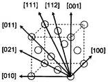
- FIG. 1 shows a face-centered cubic lattice (FCC: Face Centered Cubic lattice) together with typical crystal orientations.
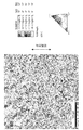
- FIG. 4 is a reverse pole figure map of 1/4 ⁇ t part of No. 4 sputtering target.
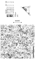
- FIG. 5 is a reverse pole figure map of 1 ⁇ 4 ⁇ t part of the sputtering target of No. 5;
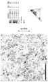
- FIG. 9 is a reverse pole figure map of 1 ⁇ 4 ⁇ t part of No. 9 sputtering target.
- the inventors of the present invention have made extensive studies in order to provide an Al-based alloy sputtering target that can reduce splash generated during sputtering film formation.
- the present invention targets a Ni-rare earth element-Al base alloy sputtering target applicable to the direct contact technique described above, and uses a Ni-rare earth element-Al base alloy sputtering target manufactured by a conventional melt casting method.
- the present inventors have studied to provide a technique that can effectively suppress the occurrence of splash even when the film is formed at a high speed and that can reduce variations in the film forming speed during the sputtering film forming process.
- the inventors have found that the intended purpose can be achieved if the crystal orientation in the normal direction of the sputtering surface of the Ni-rare earth element-Al base alloy sputtering target is appropriately controlled, and the present invention has been completed.
- “splash generation can be suppressed (reduced)” means that the occurrence of splash is generated when sputtering is performed by setting the sputtering power according to the film formation speed under the conditions described in the examples described later.
- the number average value at three locations of the surface layer portion of the sputtering target, 1/4 ⁇ t portion, 1/2 ⁇ t portion) is 21 pieces / cm 2 or less (preferably 11 pieces / cm 2 or less, more preferably 7 pieces). Means / cm 2 or less).
- the techniques of Patent Documents 2 to 9 that do not evaluate the occurrence of splash in the thickness direction. And the evaluation criteria are different.
- FIG. 1 shows a typical crystal structure and crystal orientation of a face-centered cubic lattice (FCC: Face-Centered-Cubic-lattice).
- the crystal orientation display method employs a general method. For example, [001], [010], and [100] are equivalent crystal orientations, and these three orientations are collectively expressed as ⁇ 001>. ing.
- Al has a crystal structure of a face-centered cubic lattice (FCC: Face : Centered Cubic lattice), and the normal direction of the sputtering surface of the sputtering target [direction toward the opposite substrate (ND)].
- FCC Face : Centered Cubic lattice
- ND opposite substrate
- the crystal orientation mainly includes five kinds of crystal orientations ⁇ 011>, ⁇ 001>, ⁇ 111>, ⁇ 012>, and ⁇ 112>.
- the direction with the highest atomic density (closest direction) is ⁇ 011>, followed by ⁇ 001>, ⁇ 112>, ⁇ 111>, ⁇ 012>.
- Al-based alloys and pure Al especially Al-based alloys have different solute / precipitation forms depending on the alloy system, resulting in differences in crystal deformation and rotation behavior, resulting in different crystal orientation formation processes. It is thought to come.
- JIS-5000 series Al alloys Al-Mg-based alloys
- JIS-6000 series Al alloys Al-Mg-Si alloys
- Manufacturing method guidelines have been clarified.
- Ni-rare earth element-Al-based alloys used for FPD wiring films, electrode films, reflective electrode films, etc. neither the tendency of crystal orientation nor the manufacturing method guidelines enabling crystal orientation control have been clarified It is in.
- Patent Document 7 described above describes that when a Si-containing Al-based alloy sputtering target is targeted, increasing the ⁇ 111> crystal orientation ratio increases the thin film formation rate. Further, in paragraph [0026] of Patent Document 7, a crystal having a ⁇ 111> orientation plane generates a large amount of sputtering target material having a velocity component perpendicular to the sputtering plane during sputtering due to the orientation. It is stated that it is considered to be caused by
- the present inventors have studied to provide a technique for controlling the crystal orientation in the Ni-rare earth element-Al-based alloy, among Al-based alloys.
- the crystal orientation in which the atomic density of the atoms constituting the sputtering target having a polycrystalline structure is high should be controlled as far as possible toward the substrate on which the thin film is formed. Yes.
- atoms constituting the sputtering target material are pushed out by collision with Ar ions.
- the mechanism is as follows: (a) Ar ions that collided interrupt between the atoms of the sputtering target, and the surrounding atoms are intensely affected.
- minute steps are formed between crystal grains because the erosion speed differs between crystal grains having different crystal orientations within the same sputtering plane of the sputtering target. Such a step is said to be particularly easily formed when the crystal orientation distribution is uneven or coarse crystal grains are present in the sputtering plane.
- atoms constituting the sputtering target released into the space from the surface of the sputtering target are not necessarily deposited only on the opposing substrate, and may adhere to the surrounding sputtering target surface to form a deposit. .
- This adhesion and deposition is likely to occur at the level difference between the crystal grains, and the deposit becomes a starting point of the splash, and the splash is likely to occur.
- the efficiency of the sputtering process and the yield of the sputtering target are significantly reduced.
- the present inventors have repeatedly investigated the relationship between the crystal orientation distribution, crystal grain size, and the cause of splash of the Ni-rare earth element-Al-based alloy sputtering target. It has been found that the structure of the produced Ni-rare earth element-Al-based alloy sputtering target is that uneven crystal orientation distribution and coarse crystal grains are easily formed in the sputtering surface and in the thickness direction of the sputtering target.
- the crystal orientation and crystal grain size distribution fluctuate in the plate thickness direction, and the film formation speed inherent to the sputtering target fluctuates over time. For this reason, the sputtering power is increased to increase the film formation speed during sputtering. If this is done, splash tends to occur at the part where the film formation speed unique to the sputtering target is high. On the other hand, if the sputtering power is reduced to reduce the splash, the film formation speed will drop at the part where the film formation speed specific to the sputtering target is slow. And found that there is a possibility that the productivity is remarkably lowered.
- the ratio of ⁇ 011>, ⁇ 001>, and ⁇ 112> is increased as much as possible, and the thickness of the sputtering target is further increased.
- the variation in the direction should be as small as possible, specifically, the surface layer portion of the Al-based alloy sputtering target in the direction of the thickness (t) of the Al-based alloy sputtering target, 1/4 of the thickness t.
- the crystal orientation of the Ni-rare earth element-Al-based alloy was measured using the EBSD method (EBSD: Electron Backscatter Diffraction Pattern) as follows.
- the measurement surface (parallel to the sputtering surface) is measured for the surface layer portion, 1/4 ⁇ t portion, and 1/2 ⁇ t portion in the thickness direction of the sputtering target.
- the surface is cut so that an area of 10 mm or more in length and 10 mm or more in width can be secured to obtain a sample for EBSD measurement.
- polishing with emery paper or colloidal silica suspension, etc. After polishing, electrolytic polishing with a mixed solution of perchloric acid and ethyl alcohol was performed, and the crystal orientation of the sputtering target was measured using the following apparatus and software.
- Apparatus Backscattered electron diffraction image apparatus manufactured by EDAX / TSL "Orientation Imaging Microscopy TM (OIM TM )" Measurement software: OIM Data Collection ver. 5 Analysis software: OIM Analysis ver. 5 Measurement area: area 1400 ⁇ m ⁇ 1400 ⁇ m ⁇ depth 50 nm step size: 8 ⁇ m Number of fields of view: 3 orientations in the same measurement plane Crystal orientation difference during analysis: ⁇ 15 °
- crystal orientation difference at the time of analysis: ⁇ 15 ° means, for example, in the analysis of ⁇ 001> crystal orientation, if it is within the range of ⁇ 001> ⁇ 15 °, it is regarded as an allowable range, and ⁇ 001> crystal This means that it is determined to be a bearing. This is because, if it is within the above-mentioned allowable range, it is considered that the same orientation may be considered in terms of crystallography. As shown below, in the present invention, each crystal orientation is calculated within an allowable range of ⁇ 15 °. Then, Partition Fraction of crystal orientation ⁇ uvw> ⁇ 15 ° was obtained as an area ratio.
- FIG. 2A shows No. 1 in Table 1 described in the column of Examples described later.
- 4 is a reverse pole figure map (crystal orientation map) in a 1/4 ⁇ t part of 4.
- FIG. In EBSD crystal grains having different crystal orientations can be distinguished by a color tone difference.
- each crystal orientation is identified by color, ⁇ 001> is red, ⁇ 011> is green, ⁇ 111> is blue, ⁇ 112> is magenta, and ⁇ 012> is yellow.
- 2A is shown in a black and white schematic diagram.
- R is the total area ratio of ⁇ 001> ⁇ 15 °, ⁇ 011> ⁇ 15 °, and ⁇ 112> ⁇ 15 ° (R in each part is R a for the surface layer portion and R for the 1/4 ⁇ t portion is R) b , 1 ⁇ 2 ⁇ t part is R c ), R is 0.35 or more and 0.80 or less (that is, R a , R b , R c are all 0.35 or more, 0. 80 or less)
- the total area ratio is the total area of the crystal orientations measured at each of the surface layer portion (R a ), 1/4 ⁇ t portion (R b ), and 1/2 ⁇ t portion (R c ). This means the ratio (the above measurement area (ratio to 1400 ⁇ m ⁇ 1400 ⁇ m)), and in the present invention, R a to R c are sometimes collectively expressed as R.
- the main sputtering target surface exists in the normal direction of the target surface.
- the area ratios of five crystal orientations, ⁇ 001>, ⁇ 011>, ⁇ 111>, ⁇ 112>, and ⁇ 012>, which are crystal orientations, were measured by the EBSD method with an allowable crystal orientation difference of ⁇ 15 °, respectively.
- the total area ratio (R) of ⁇ 011>, ⁇ 001>, and ⁇ 112> in each of the above locations which is a crystal orientation in which the atomic number density of the Al-based alloy is relatively high, is 0.35 or more. , 0.80 or less (ie, R a , R b , and R c are all in the range of 0.35 or more and 0.80 or less).
- R a , R b , and R c are all in the range of 0.35 or more and 0.80 or less.
- the R value is less than 0.35, the crystal orientation distribution is insufficient, and coarse crystal grains are formed, so that the occurrence of splash cannot be suppressed effectively.
- the R value exceeds 0.80 coarse crystal grains are easily formed, and the occurrence of splash cannot be suppressed. Controlling the R value to preferably 0.4 or more and 0.75 or less is desirable because it can further suppress the occurrence of splash.
- the ratio of the crystal orientation ( ⁇ 111>, ⁇ 012>) that is the measurement target of the present invention other than the above ⁇ 011>, ⁇ 001>, ⁇ 112> is not particularly limited.
- the crystal orientation of ⁇ 011>, ⁇ 001>, and ⁇ 112> may be controlled so as to satisfy the requirements (1) and (2). Experiments have confirmed that the influence of the orientation ( ⁇ 111>, ⁇ 012>) need not be taken into account.
- the Al-based alloy sputtering target of the present invention may have an average crystal grain size of 40 ⁇ m or more and 450 ⁇ m or less when a boundary between pixels having a crystal orientation difference of 15 ° or more measured by the EBSD method is a grain boundary. preferable.
- the analysis software When analyzing the crystal orientation data (1 visual field size: 1400 ⁇ m ⁇ 1400 ⁇ m, step size: 8 ⁇ m) measured by the EBSD method, and the boundary between pixels having a crystal orientation difference of 15 ° or more is a grain boundary, the analysis software Let D be the average value of equivalent circle diameters determined from the grain size distribution of Grain Size (Diameter) output at 1.
- D the average value of equivalent circle diameters determined from the grain size distribution of Grain Size (Diameter) output at 1.
- the thickness of the sputtering target is t
- D at each location determined in the surface layer portion, 1/4 ⁇ t portion, and 1/2 ⁇ t portion in the thickness direction of the sputtering target is the surface layer.
- the part is D a
- the 1/4 ⁇ t part is D b
- the 1/2 ⁇ t part is D c .
- the average crystal grain size is smaller, specifically, the average crystal grain size is preferably 450 ⁇ m or less, more preferably 180 ⁇ m or less, and still more preferably. 120 ⁇ m or less.
- the lower limit of the average crystal grain size may be determined in relation to the production method. That is, in the present invention, a melting casting method for producing an ingot from an Al alloy molten metal is desirable from the viewpoint of production cost, production process reduction, yield improvement, etc., but in the case of the melting casting method, the average crystal grain size is Since it is impossible to produce an Al-based alloy sputtering target of less than 40 ⁇ m using general melting and casting equipment, the lower limit of the average crystal grain size was set to 40 ⁇ m.
- the Al-based alloy sputtering target of the present invention preferably has a Vickers hardness (HV) of 26 or more. According to the examination results of the present inventors, it has been found that when a Ni-rare earth element-Al-based alloy sputtering target is used, splash is likely to occur if the sputtering target has low hardness.
- the Vickers hardness (HV) of the Al-based alloy sputtering target of the present invention is preferably as high as possible from the viewpoint of preventing the occurrence of splash, and is preferably 26 or more, more preferably 35 or more, and still more preferably 40 or more. Even more preferably, it is 45 or more.
- the upper limit of Vickers hardness is not particularly limited, but if it is too high, it is necessary to increase the rolling rate of cold rolling for adjusting the hardness, and in that case, production problems such as difficulty in rolling occur. Therefore, the Vickers hardness is preferably 160 or less, more preferably 140 or less, and still more preferably 120 or less.
- the upper limit and the lower limit of the Vickers hardness can be arbitrarily combined to make the range of the Vickers hardness.
- Ni-rare earth element-Al base alloy which is the subject of the present invention will be described.
- the present invention is directed to the Al-based alloy sputtering target containing Ni and rare earth elements. This is because, as described in Patent Document 1, when a film is formed for wiring using a Ni-rare earth element-Al-based alloy, it has excellent heat resistance and is therefore extremely useful as a wiring material for direct contact. .
- Ni is an element effective for reducing the contact electric resistance between the Al-based alloy film and the pixel electrode that is in direct contact with the Al-based alloy film. It is also useful for controlling crystal orientation and crystal grain size, which are useful for preventing the occurrence of splash.
- Ni at least 0.05 atomic% or more.
- the Ni content is more preferably 0.07 atomic% or more, and still more preferably 0.1 atomic% or more.
- the electrical resistivity of the Al-based alloy film is increased, so that the content is preferably 2.0 atomic% or less. More preferably, it is 1.5 atomic% or less, More preferably, it is 1.1 atomic% or less.
- the upper limit and lower limit of the Ni content can be arbitrarily combined to make the Ni content range.
- the rare earth element is an element effective for improving the heat resistance of an Al-based alloy film formed using this Al-based alloy sputtering target and preventing hillocks formed on the surface of the Al-based alloy film. . It is also useful for controlling crystal orientation and crystal grain size, which are useful for preventing the occurrence of splash.
- the rare earth element In order to exert such an effect, it is preferable to contain at least 0.1 atomic% of the rare earth element.
- a more preferable rare earth element content is 0.2 atomic% or more, and further preferably 0.3 atomic% or more.
- the content of the rare earth element is excessively increased, the electrical resistivity of the Al-based alloy film is increased. More preferably, it is 0.8 atomic% or less, More preferably, it is 0.6 atomic% or less.
- the upper limit and the lower limit of the rare earth element content can be arbitrarily combined to make the rare earth element content range.
- an Al—Ni—Al base alloy sputtering target further containing a rare earth element such as Nd or La is also targeted.
- rare earth element means Y, lanthanoid element, and actinoid element in the periodic table, particularly when a Ni-rare earth element-Al-based alloy sputtering target containing La and Nd is used. Is preferably used.
- the rare earth elements may be contained alone or in combination of two or more. When using 2 or more types together, it is desirable that the total content of rare earth elements is within the above range.
- the Al-based alloy sputtering target of the present invention contains Ge.
- Ge is an element effective for improving the corrosion resistance of an Al-based alloy film formed using the Al-based alloy sputtering target of the present invention. It is also useful for controlling crystal orientation and crystal grain size, which are useful for preventing the occurrence of splash.
- Ge In order to exert such an action, it is preferable to contain Ge at least 0.10 atomic%.
- a more preferable Ge content is 0.2 atomic% or more, and further preferably 0.3 atomic% or more.
- the electrical resistivity of the Al-based alloy film is increased.
- the Ge content is more preferably 0.8 atomic percent or less, and still more preferably 0.6 atomic percent or less.
- the upper limit and the lower limit of the Ge content can be arbitrarily combined to make the Ge content range.
- the Al-based alloy of the present invention preferably contains Ti and B in addition to Ni and rare earth elements, more preferably Ge.
- Ti and B are elements that contribute to the refinement of crystal grains, and the addition of Ti and B increases the range of manufacturing conditions (allowable range). However, if added excessively, the electrical resistivity of the Al-based alloy film may be increased.
- the Ti content is preferably 0.0002 atomic% or more, more preferably 0.0004 atomic% or more, preferably 0.012 atomic% or less, more preferably 0.006 atomic% or less.
- the upper limit and the lower limit of the Ti content can be arbitrarily combined to make the range of the Ti content.
- the B content is preferably 0.0002 atomic% or more, more preferably 0.0004 atomic% or more, and is preferably 0.012 atomic% or less, more preferably 0.006 atomic% or less.
- the upper limit and the lower limit of the B content can be arbitrarily combined to make the B content range.
- Al—Ti—B For addition of Ti and B, a commonly used method can be adopted, and typically, it is added to the molten metal as an Al—Ti—B refining agent.
- the composition of Al—Ti—B is not particularly limited as long as a desired Al-based alloy sputtering target can be obtained.
- Al-5 mass% Ti-1 mass% B, Al-5 mass% Ti— 0.2 mass B or the like is used. These can use a commercial item.
- the components of the Al-based alloy used in the present invention preferably contain Ni and a rare earth element, and the balance is Al and unavoidable impurities, and more preferably the balance Al and unavoidable impurities contain Ni, rare earth elements and Ge. . More preferably, it is Ni, rare earth elements, Ge, Ti, B, and the balance Al and inevitable impurities.
- Inevitable impurities include elements inevitably mixed in the manufacturing process, for example, Fe, Si, C, O, N, etc., and the content of each element is 0.05 atomic% or less. It is preferable.
- Ni-rare earth element-Al base alloy which is the object of the present invention has been described.
- an Al-based alloy sputtering target it is desirable to manufacture an Al-based alloy sputtering target using a melt casting method.
- a hot rolling ⁇ annealing in order to produce an Al-based alloy sputtering target in which the crystal orientation distribution and crystal grain size are appropriately controlled, in the process of melting casting ⁇ (soaking as necessary) ⁇ hot rolling ⁇ annealing, Heat conditions (soaking temperature, soaking time, etc.), hot rolling conditions (eg rolling start temperature, rolling end temperature, 1-pass maximum rolling reduction, total rolling reduction, etc.), annealing conditions (annealing temperature, annealing time, etc.) It is preferable to appropriately control at least one of them. You may perform cold rolling-> annealing (2nd rolling-> annealing process) after the said process.
- the second rolling ⁇ annealing process described above is performed, and cold rolling (cold rolling ratio, etc.) conditions are controlled.
- cold rolling cold rolling ratio, etc.
- melt casting The melt casting process is not particularly limited, and a process normally used for the production of a sputtering target may be appropriately adopted to ingot a Ni-rare earth element-Al base alloy ingot.
- typical casting methods include DC (semi-continuous) casting, thin plate continuous casting (double roll type, belt caster type, propel type, block caster type, etc.).
- the soaking temperature is about 300 to 600 ° C. (more preferably 400 to 550 ° C.), and the soaking time is about 1 to 8 hours (more preferably 4 to 8). Time).
- hot rolling After performing the above-mentioned soaking as required, hot rolling is performed. In order to control the crystal orientation distribution and the crystal grain size, it is desirable to appropriately control the hot rolling start temperature. If the hot rolling start temperature is too low, the deformation resistance increases, and rolling may not be continued to a desired plate thickness.
- the preferred hot rolling start temperature is 210 ° C. or higher, more preferably 220 ° C. or higher, and even more preferably 230 ° C. or higher. On the other hand, if the hot rolling start temperature is too high, the distribution of crystal orientation in the normal direction of the sputtering surface may vary or the crystal grain size may increase, resulting in an increased number of splashes. .
- a preferable hot rolling start temperature is 410 ° C. or lower, more preferably 400 ° C. or lower, and further preferably 390 ° C. or lower.
- the upper limit and the lower limit of the hot rolling start temperature can be arbitrarily combined to make the hot rolling start temperature range.
- the hot rolling end temperature is too high, the crystal orientation distribution in the normal direction of the sputtering surface may vary, or the crystal grain size may become coarse, so preferably 220 ° C. or less, more preferably 210 ° C. or less, More preferably, it is 200 degrees C or less.
- the hot rolling end temperature is too low, the deformation resistance increases, and rolling may not be continued to a desired plate thickness. Therefore, it is preferably 50 ° C. or higher, more preferably 70 ° C. or higher, and still more preferably 90 ° C. That's it.
- the upper limit and the lower limit of the hot rolling end temperature can be arbitrarily combined to make the hot rolling end temperature range.
- a preferable one-pass maximum rolling reduction is 3% or more, more preferably 6% or more, and still more preferably 9% or more.
- the one-pass maximum rolling reduction is preferably 25% or less, more preferably 20% or less, and still more preferably 15% or less.
- the upper limit and lower limit of the one-pass maximum rolling reduction can be arbitrarily combined to make the range of the one-pass maximum rolling reduction.
- a preferable total rolling reduction is 68% or more, more preferably 70% or more, and further preferably 75% or more.
- a preferable total rolling reduction is 95% or less, more preferably 90% or less, and still more preferably 85% or less.
- the upper limit and the lower limit of the total rolling reduction can be arbitrarily combined to make the range of the total rolling reduction.
- Reduction ratio per pass (%) ⁇ (thickness before one pass of rolling) ⁇ (thickness after one pass of rolling) ⁇ / (thickness before one pass of rolling) ⁇ 100
- Total rolling reduction (%) ⁇ (Thickness before starting rolling) ⁇ (Thickness after finishing rolling) ⁇ / (Thickness before starting rolling) ⁇ 100
- annealing After hot rolling as described above, annealing is performed. In order to control the crystal orientation distribution and the crystal grain size, when the annealing temperature is increased, the crystal grain size tends to be coarsened, and therefore, it is preferably 450 ° C. or lower. Further, if the annealing temperature is too low, a desired crystal orientation cannot be obtained, or coarse crystal grains may remain without being refined, so 250 ° C. or more (more preferably 300 to 400 ° C.). It is preferable to do. It is preferable to control the annealing time to about 1 to 10 hours (more preferably 2 to 4 hours).
- the crystal orientation distribution and crystal grain size of the Ni-rare earth element-Al-based alloy sputtering target can be controlled by the above manufacturing method, but after that, further cold rolling ⁇ annealing (second rolling, annealing) is performed. Also good.
- the cold rolling conditions are not particularly limited, but it is preferable to control the annealing conditions. For example, it is recommended to control the annealing temperature within the range of 150 to 250 ° C. (more preferably 180 to 220 ° C.) and the annealing time within the range of 1 to 5 hours (more preferably 2 to 4 hours).
- the hardness of the Ni-rare earth element-Al-based alloy sputtering target since the hardness cannot be sufficiently increased if the rolling rate in cold rolling is too low, it is preferably 15% or more, more preferably Is preferably 20% or more. On the other hand, if the rolling rate is increased too much, the deformation resistance increases, and rolling cannot be continued to a desired plate thickness. Therefore, it is preferably 35% or less, and more preferably 30% or less.
- the upper limit and lower limit of the said rolling rate can be combined arbitrarily, and it can also be set as the range of the said rolling rate.
- Example 1 Various Ni-rare earth element-Al base alloys shown in Table 1 were prepared, and ingots having a thickness of 100 mm were formed by DC casting, and then hot rolled and annealed under the conditions shown in Table 1 to obtain rolled sheets Was made. For reference, the thickness of the produced rolled plate is shown in Table 1.
- Ni-rare earth element-Al base alloy containing Ti and B was prepared by adding Ti and B to the molten metal in the form of a refining agent (Al-5 mass% Ti-1 mass% B).
- a refining agent Al-5 mass% Ti-1 mass% B.
- No. No. 5 Ni-rare earth element-Al base alloy Ti: 0.0005 atomic%, B: 0.0005 atomic%)
- the agent was added at a rate of 0.02% by mass.
- No. 6 Ni-rare earth element-Al base alloy Ti: 0.0046 atomic%, B: 0.0051 atomic%)
- the agent was added at a rate of 0.2% by weight.
- cold rolling and annealing (2 hours at 200 ° C.) were performed on the rolled sheet.
- the cold rolling ratio during cold rolling was set to 22%.
- the cold rolling rate was 5%.
- machining rounding and lathe processing
- the surface layer portion, 1/4 ⁇ t portion, 1/2 ⁇ t portion toward the thickness (t) direction of the rolled plate Manufactures three disc-shaped Ni-rare earth element-Al-based alloy sputtering targets (size: diameter 101.6 mm x thickness 5.0 mm) with the thickness adjusted by a lathe process so that becomes the sputtering surface did.
- Crystal orientation, average crystal grain size Using the above sputtering target, the crystal orientation in the normal direction of the sputtering surface was measured and analyzed based on the above-described EBSD method, and the R a , R b , R c , R ave value and average crystal grain size were determined. When any value of R a , R b , and R c deviated from R ave ⁇ 20%, it was determined that the variation of the R value in the thickness direction of the sputtering target was large.
- the Vickers hardness (HV) of each sputtering target was measured using a Vickers hardness meter (AVK-G2 manufactured by Akashi Seisakusho Co., Ltd.).
- Sputtering device HSR-542S manufactured by Shimadzu Corporation Sputtering conditions: Back pressure: 3.0 ⁇ 10 ⁇ 6 Torr or less, Ar gas pressure: 2.25 ⁇ 10 ⁇ 3 Torr, Ar gas flow rate: 30 sccm, Sputtering power: DC260W Distance between electrodes: 52mm, Substrate temperature: room temperature, Sputtering time: 120 seconds, Glass substrate: CORNING # 1737 (diameter 50.8 mm, thickness 0.7 mm), Stylus type film thickness meter: alpha-step 250 manufactured by TENCOR INSTRUMENTS
- the film formation rate was calculated based on the following formula.
- Deposition rate (nm / s) thin film thickness (nm) / sputtering time (s)
- the film formation speed in each example is a high-speed film formation of 2.2 nm / s or more, and measurement is performed at three arbitrary locations.
- the film formation speed at each measurement position fluctuates by 8% or more from the average value, It was determined that there was a variation in film speed.
- the position coordinates, size (average particle diameter), and number of particles recognized on the surface of the thin film were measured.
- particles having a size of 3 ⁇ m or more are regarded as particles.
- the surface of the thin film was observed with an optical microscope (magnification: 1000 times), a hemispherical shape was regarded as a splash, and the number of splashes per unit area was measured.
- the number of splashes was measured in the same manner at three locations of the surface layer portion, 1/4 ⁇ t portion, and 1/2 ⁇ t portion of the sputtering target, and the number of splashes at the three measured locations was measured.
- the average value was defined as “the number of occurrences of splash”.
- the number of occurrences of splash thus obtained is 7 / cm 2 or less, ⁇ , 8 to 11 / cm 2 , and 12 to 21 / cm 2 .
- delta) and 22 piece / cm ⁇ 2 > or more were evaluated as x.
- the number of splash occurrences of 21 / cm 2 or less was evaluated as having an effect of suppressing the occurrence of splash (pass).
- a sample for measuring the electrical resistivity of the thin film was prepared by the following procedure.
- a positive photoresist novolak resin: TSMR-8900 manufactured by Tokyo Ohka Kogyo Co., Ltd., thickness 1.0 ⁇ m, line width 100 ⁇ m
- TSMR-8900 positive photoresist
- the overall performance was evaluated, and the result was designated as “total judgment”.
- the sputtering target was evaluated as ⁇ , ⁇ , or ⁇
- the thin film property was evaluated as ⁇ , ⁇ , or ⁇ as it was.
- the judgment of the characteristics of the sputtering target was ⁇ , ⁇ , or ⁇ , and the thin film properties of x were evaluated as x.
- the determination of the characteristics of the sputtering target was x, and the thin film characteristics were evaluated as x.
- the evaluation of the characteristics of the sputtering target was x, and the thin film characteristics of x were evaluated as x.
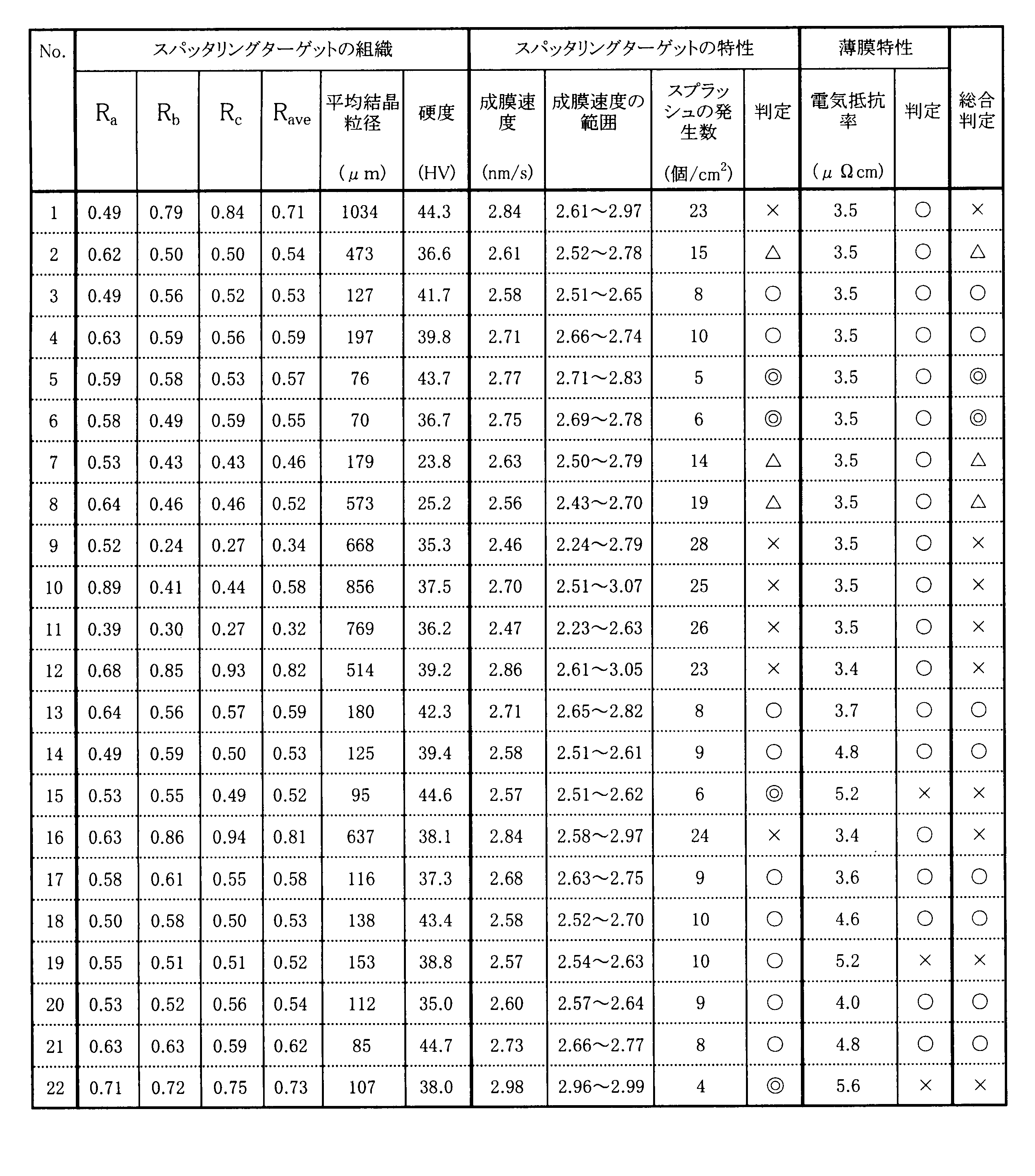
- no. 2 is an example in which the alloy composition, crystal orientation distribution (range of R a to R c value and R ave value), and Vickers hardness satisfy the requirements of the present invention, and the number of occurrences of splash is 21 / cm 2. It was suppressed below and the effect which suppresses generation
- No. 7 is an example in which the alloy composition, the crystal orientation distribution, and the average crystal grain size satisfy the requirements of the present invention.
- the number of occurrences of splash is suppressed to 21 pieces / cm 2 or less, and the effect of suppressing the occurrence of splash is obtained. Admitted.
- no. No. 7 has a cold rolling rate lower than the lower limit (15%) recommended in the present invention, so that the occurrence of splash is suppressed compared to an example in which the Vickers hardness is less than 26 and the Vickers hardness is controlled to 26 or more. The effect was reduced.
- No. No. 8 is an example in which the alloy composition and the crystal orientation distribution satisfy the requirements of the present invention.
- the number of occurrences of splash was suppressed to 21 pieces / cm 2 or less, and the effect of suppressing the occurrence of splash was recognized.
- no. In No. 8 since the rolling start temperature exceeds the upper limit (410 ° C.) recommended in the present invention, the average grain size exceeds the upper limit value (450 ⁇ m) recommended in the present invention, and the cold rolling rate is Since it is below the lower limit (15%) recommended in the invention, the dispersion of the R value in the thickness direction of the sputtering target is increased, the Vickers hardness is also less than 26, and the average crystal grain size and Vickers hardness are in the preferred ranges. Compared to the controlled example, the effect of suppressing the occurrence of splash was reduced.
- No. 3 to 6, 13, 14, 17, 18, 20, and 21 are examples in which the cold rolling ratio during the second rolling is appropriately controlled, and in addition to the alloy composition and the average crystal grain size, the Vickers hardness is also the present invention. Meets the recommended requirements. Therefore, the number of occurrences of splash is further suppressed (the number of occurrences of splash: 11 pieces / cm 2 or less), and the effect of suppressing the occurrence of higher splash was recognized.
- No. 1 No. 1 is an example manufactured under conditions where the amount of Ni is small and below the lower limit (68%) of the total rolling reduction recommended in the present invention.
- the total area ratio of R c exceeds 0.80, the variation is increased in the thickness direction of the sputtering target R value, and the crystal grain size becomes coarse, the number of occurrences of splash is increased .
- No. 9 is a condition in which the hot rolling start temperature (410 ° C.) and the rolling end temperature (220 ° C.) are higher than the upper limit recommended in the present invention, and the total rolling reduction is lower than the lower limit (68%) recommended in the present invention. It is an example manufactured by. In this example, the total area ratio of R b and R c is less than 0.35, the variation of the R value in the thickness direction of the sputtering target is large, the crystal grain size is coarse, and the number of occurrences of splash is small. Increased. In addition, the film forming speed varied.
- No. 10 is an example in which the one-pass maximum rolling reduction during hot rolling is less than the lower limit (3%) recommended in the present invention, and the rolling start temperature is the upper limit (410 ° C. recommended in the present invention). ) Is exceeded.
- the total area ratio of R a is more than 0.80, the variation is increased in the thickness direction of the sputtering target R value, and the crystal grain size becomes coarse, the number of occurrences of splash is increased.
- No. 11 is an example in which the total rolling reduction during hot rolling is less than the lower limit recommended by the present invention (68%), and the total area ratio of R b and R c is less than 0.35, The variation of the R value in the thickness direction of the sputtering target increased, the crystal grain size became coarse, and the number of occurrences of splash increased. In addition, the film forming speed varied.
- No. No. 12 is an example in which the amount of Ge is small and the total rolling reduction during hot rolling is less than the lower limit (68%) recommended in the present invention, and the total area ratio of R b and R c is 0.
- the variation of the R value in the thickness direction of the sputtering target increased, the crystal grain size became coarse, and the number of occurrences of splash increased.
- the film forming speed varied.
- No. No. 16 is an example in which the amount of Nd is small and the total rolling reduction ratio during hot rolling is less than the lower limit (68%) recommended in the present invention, and the total area ratio of R b and R c is 0.
- the variation of the R value in the thickness direction of the sputtering target increased, the crystal grain size became coarse, and the number of occurrences of splash increased.
- the film forming speed varied.
- No. 15 (Ge), 19 (Nd), and 22 (Ni) are examples in which the content of the alloy element was increased, and the effect of reducing the splash was recognized, but the electrical resistivity of the thin film increased.
- FIG. 9 shows a reverse pole figure map (crystal orientation map) for a 1 ⁇ 4 ⁇ t part of 9 (comparative example).
- the film formation speed can be stabilized even when the film is formed at high speed. Sputtering defects (splash) are also effectively suppressed.
- the deposition rate can be stably maintained from the start to the end of target use, the splash generated during the sputtering target deposition and the variation in deposition rate can be greatly reduced. Can be improved.
Landscapes
- Chemical & Material Sciences (AREA)
- Engineering & Computer Science (AREA)
- Materials Engineering (AREA)
- Mechanical Engineering (AREA)
- Metallurgy (AREA)
- Organic Chemistry (AREA)
- Chemical Kinetics & Catalysis (AREA)
- Physical Vapour Deposition (AREA)
Abstract
Description
[1] Niおよび希土類元素を含有するAl基合金スパッタリングターゲットであって、後方散乱電子回折像法によって前記Al基合金スパッタリングターゲットの表層部、1/4×t(t:Al基合金スパッタリングターゲットの厚さ)部、1/2×t部の各スパッタリング面の法線方向の結晶方位<001>、<011>、<111>、<012>および<112>を観察したとき、下記(1)、(2)の要件を満足するAl基合金スパッタリングターゲット。
(1)前記<001>±15°、前記<011>±15°および前記<112>±15°の合計面積率をR(各箇所のRは、前記表層部はRa、前記1/4×t部はRb、前記1/2×t部はRcとする)としたとき、Rが、0.35以上、0.80以下であり、かつ
(2)前記Ra、前記Rb、および前記Rcが、R平均値[Rave=(Ra+Rb+Rc)/3]の±20%の範囲内にある。
[2] 前記Al基合金スパッタリングターゲットのスパッタリング面を後方散乱電子回折像法によって結晶粒径を観察したとき、平均結晶粒径が40~450μmである[1]に記載のAl基合金スパッタリングターゲット。
[3] 前記Niの含有量が0.05~2.0原子%、前記希土類元素の含有量が0.1~1.0原子%である[1]または[2]に記載のAl基合金スパッタリングターゲット。
[4] 更にGeを含有する[1]~[3]のいずれか一つに記載のAl基合金スパッタリングターゲット。
[5] 前記Geの含有量が0.10~1.0原子%である[4]に記載のAl基合金スパッタリングターゲット。
[6] 更にTiおよびBを含有する[1]~[5]のいずれか一つに記載のAl基合金スパッタリングターゲット。
[7] 前記Tiの含有量が0.0002~0.012原子%、前記Bの含有量が0.0002~0.012原子%である[6]に記載のAl基合金スパッタリングターゲット。
[8] 前記Al基合金スパッタリングターゲットのビッカース硬さが26以上である[1]~[7]のいずれか一つに記載のAl基合金スパッタリングターゲット。
「Orientation Imaging MicroscopyTM(OIMTM)」
測定ソフトウェア:OIM Data Collection ver.5
解析ソフトウェア:OIM Analysis ver.5
測定領域:面積1400μm×1400μm×深さ50nm
step size:8μm
測定視野数:同一測定面内において、3視野
解析時の結晶方位差:±15°
本発明で合計面積率とは、表層部(Ra)、1/4×t部(Rb)、1/2×t部(Rc)のそれぞれの箇所で測定した上記結晶方位の合計面積率(上記測定面積(1400μm×1400μmに対する比率)を意味し、本発明ではRa~Rcをまとめて単にRで表記することがある。
さらに、スパッタリングターゲットの厚さをtとしたとき、スパッタリングターゲットの板厚方向に向って表層部、1/4×t部、1/2×t部の3箇所において求めた各R値(各箇所のR値を表層部はRa、1/4×t部をRb、1/2×t部をRcとする)が、R値の平均値[Rave=(Ra+Rb+Rc)/3]の±20%の範囲内にあることとした(すなわち、Ra、Rb、Rcは全てRave±20%の範囲内)。これは、各測定位置でのR値(Ra、Rb、Rc)がR値の平均値Raveの±20%から外れると、スパッタリング面法線方向の結晶方位の分布にばらつきが生じ、スパッタリングターゲットの成膜速度が時間の経過と共に不安定になり、スパッタリング成膜過程での成膜速度のばらつきが生じたり、また、スプラッシュの発生頻度が増大する。
本発明のAl基合金スパッタリングターゲットは、EBSD法によって測定される結晶方位差が15°以上のピクセル間の境界を結晶粒界としたときの平均結晶粒径を40μm以上、450μm以下とすることが好ましい。
更に本発明のAl基合金スパッタリングターゲットは、ビッカース硬さ(HV)が26以上であることが好ましい。本発明者らの検討結果によれば、Ni-希土類元素-Al基合金スパッタリングターゲットを用いたとき、このスパッタリングターゲットの硬さが低いとスプラッシュが発生し易くなることが判明したからである。その理由は、詳細には不明であるが、スパッタリングターゲットの硬さが低いと、スパッタリングターゲットの製造に用いるフライス盤や旋盤などによる機械加工の仕上げ面の微視的平滑さが悪化するため、すなわち、素材表面が複雑に変形し、粗くなるため、機械加工に用いる切削油等の汚れがスパッタリングターゲットの表面に取り込まれて残留する。このような残留汚れは、後工程で表面洗浄を行っても十分に取り除くことが困難であり、このようなスパッタリングターゲット表面に残留した汚れが、スプラッシュの発生起点になっていると推測される。したがってこのような汚れをスパッタリングターゲットの表面に残留させないようにするには、機械加工時の加工性(切れ味)を改善し、素材表面が粗くならないようにすることが必要である。そのため本発明では、スパッタリングターゲットの硬さを高めることが望ましい。
次に、上記Al基合金スパッタリングターゲットを製造する方法について説明する。
溶解鋳造工程は特に限定されず、スパッタリングターゲットの製造に通常用いられる工程を適宜採用し、Ni-希土類元素-Al基合金鋳塊を造塊すればよい。例えば鋳造方法として、代表的にはDC(半連続)鋳造、薄板連続鋳造(双ロール式、ベルトキャスター式、プロペルチ式、ブロックキャスター式など)などが挙げられる。
上記のようにしてNi-希土類元素-Al基合金鋳塊を造塊した後、熱間圧延を行なうが、必要に応じて、均熱を行ってもよい。結晶方位分布および結晶粒径制御のためには、均熱温度をおおむね300~600℃程度(より好ましくは400~550℃)、均熱時間をおおむね1~8時間程度(より好ましくは4~8時間)に制御することが好ましい。
上記の均熱を必要に応じて行なった後、熱間圧延を行なう。結晶方位分布および結晶粒径制御のためには、熱間圧延開始温度を適切に制御にすることが望ましい。熱間圧延開始温度が低すぎると変形抵抗が高くなり、所望の板厚まで圧延が継続できなくなることがある。好ましい熱間圧延開始温度は210℃以上、より好ましくは220℃以上、更により好ましくは230℃以上である。一方、熱間圧延開始温度を高くしすぎると、スパッタリング面法線方向の結晶方位の分布にばらつきが生じたり、結晶粒径が粗大化するなどして、スプラッシュの発生数が多くなることがある。好ましい熱間圧延開始温度は410℃以下、より好ましくは400℃以下、更に好ましくは390℃以下である。なお、上記熱間圧延開始温度の上限と下限を任意に組み合わせて上記熱間圧延開始温度の範囲とすることもできる。
1パス当たりの圧下率(%)={(圧延1パス前の厚さ)-(圧延1パス後の厚さ)}/(圧延1パス前の厚さ)×100
総圧下率(%)={(圧延開始前の厚さ)-(圧延終了後の厚さ)}/(圧延開始前の厚さ)×100
上記のようにして熱間圧延を行なった後、焼鈍する。結晶方位分布および結晶粒径制御のためには、焼鈍温度を高くすると、結晶粒径が粗大化する傾向にあるため、450℃以下とすることが好ましい。また焼鈍温度が低すぎると、所望の結晶方位が得られなかったり、結晶粒が微細化されずに粗大な結晶粒が残留することがあるので250℃以上(より好ましくは300~400℃)とすることが好ましい。焼鈍時間はおおむね1~10時間程度(より好ましくは2~4時間)に制御することが好ましい。
上記の製法によりNi-希土類元素-Al基合金スパッタリングターゲットの結晶方位分布および結晶粒径を制御することができるが、その後に、更に冷間圧延→焼鈍(2回目の圧延、焼鈍)を行なってもよい。結晶方位分布および結晶粒径制御する観点からは、冷間圧延条件は特に限定されないものの、焼鈍条件を制御することが好ましい。例えば焼鈍温度は150~250℃(より好ましくは180~220℃)、焼鈍時間は1~5時間(より好ましくは2~4時間)の範囲に制御することが推奨される。
表1に示す種々のNi-希土類元素-Al基合金を用意し、厚み100mmの鋳塊をDC鋳造法によって造塊した後、表1に記載の条件で熱間圧延および焼鈍を行って圧延板を作製した。参考のため、作製した圧延板の厚さを表1に示す。
上記のスパッタリングターゲットを用い、前述したEBSD法に基づき、スパッタリング面法線方向の結晶方位を測定し、解析してRa、Rb、Rc、Rave値と平均結晶粒径を求めた。Ra、Rb、Rcのいずれかの値がRave±20%を外れた場合を、R値のスパッタリングターゲットの厚さ方向におけるばらつきが大きいと判断した。
上記各スパッタリングターゲットのビッカース硬さ(HV)は、ビッカース硬度計(株式会社明石製作所製、AVK-G2)を用いて測定した。
下記の条件でスパッタリングを行い、ガラス基板上に薄膜を成膜した。得られた薄膜の厚さを触針式膜厚計によって測定した。
スパッタリング条件:
背圧:3.0×10⁻⁶Torr以下、
Arガス圧:2.25×10⁻³Torr、
Arガス流量:30sccm、
スパッタリングパワー:DC260W、
極間距離:52mm、
基板温度:室温、
スパッタリング時間:120秒、
ガラス基板:CORNING社製#1737(直径50.8mm、厚さ0.7mm)、
触針式膜厚計:TENCOR INSTRUMENTS製alpha-step 250
成膜速度(nm/s)=薄膜の厚さ(nm)/スパッタリング時間(s)
本実施例では、高スパッタリングパワーの条件下で発生しやすいスプラッシュの発生数を測定し、スプラッシュの発生を評価した。
Y値=成膜速度(2.74nm/s)×スパッタリングパワー(260W)=713
成膜速度:2.77nm/s
下式に基づき、スパッタリングパワーDCを257Wと設定スパッタリングパワー
DC=Y値(713)/成膜速度(2.77)≒257W
薄膜の電気抵抗率測定用サンプルは、以下の手順で作製した。上記の薄膜表面上に、フォトリソグラフィによってポジ型フォトレジスト(ノボラック系樹脂:東京応化工業製TSMR-8900、厚さ1.0μm、線幅100μm)をストライプパターン形状に形成した。ウェットエッチングによって線幅100μm、線長10mmの電気抵抗率測定用パターン形状に加工した。ウェットエッチングにはH3PO4:HNO3:H2O=75:5:20の混合液を用いた。熱履歴を与えるため、前記エッチング処理後に、CVD装置内の減圧窒素雰囲気(圧力:1Pa)を用いて250℃で30分保持する雰囲気熱処理を行なった。その後、四探針法により電気抵抗率を室温で測定し、5.0μΩcm以下のものを良好(○)、5.0μΩcm超のものを不良(×)と評価した。

本出願は、2010年2月26日出願の日本特許出願(特願2010-043073)に基づくものであり、その内容はここに参照として取り込まれる。
Claims (37)
- Niおよび希土類元素を含有するAl基合金スパッタリングターゲットであって、後方散乱電子回折像法によって前記Al基合金スパッタリングターゲットの表層部、1/4×t(t:Al基合金スパッタリングターゲットの厚さ)部、1/2×t部の各スパッタリング面の法線方向の結晶方位<001>、<011>、<111>、<012>および<112>を観察したとき、下記(1)、(2)の要件を満足するAl基合金スパッタリングターゲット。
(1)前記<001>±15°、前記<011>±15°および前記<112>±15°の合計面積率をR(各箇所のRは、前記表層部はRa、前記1/4×t部はRb、前記1/2×t部はRcとする)としたとき、Rが、0.35以上、0.80以下であり、かつ
(2)前記Ra、前記Rb、および前記Rcが、R平均値[Rave=(Ra+Rb+Rc)/3]の±20%の範囲内にある。 - 前記Al基合金スパッタリングターゲットのスパッタリング面を後方散乱電子回折像法によって結晶粒径を観察したとき、平均結晶粒径が40~450μmである請求項1に記載のAl基合金スパッタリングターゲット。
- 前記Niの含有量が0.05~2.0原子%、前記希土類元素の含有量が0.1~1.0原子%である請求項1に記載のAl基合金スパッタリングターゲット。
- 前記Niの含有量が0.05~2.0原子%、前記希土類元素の含有量が0.1~1.0原子%である請求項2に記載のAl基合金スパッタリングターゲット。
- 更にGeを含有する請求項1に記載のAl基合金スパッタリングターゲット。
- 更にGeを含有する請求項2に記載のAl基合金スパッタリングターゲット。
- 更にGeを含有する請求項3に記載のAl基合金スパッタリングターゲット。
- 更にGeを含有する請求項4に記載のAl基合金スパッタリングターゲット。
- 前記Geの含有量が0.10~1.0原子%である請求項5に記載のAl基合金スパッタリングターゲット。
- 前記Geの含有量が0.10~1.0原子%である請求項6に記載のAl基合金スパッタリングターゲット。
- 前記Geの含有量が0.10~1.0原子%である請求項7に記載のAl基合金スパッタリングターゲット。
- 前記Geの含有量が0.10~1.0原子%である請求項8に記載のAl基合金スパッタリングターゲット。
- 更にTiおよびBを含有する請求項1に記載のAl基合金スパッタリングターゲット。
- 更にTiおよびBを含有する請求項2に記載のAl基合金スパッタリングターゲット。
- 更にTiおよびBを含有する請求項3に記載のAl基合金スパッタリングターゲット。
- 更にTiおよびBを含有する請求項4に記載のAl基合金スパッタリングターゲット。
- 更にTiおよびBを含有する請求項5に記載のAl基合金スパッタリングターゲット。
- 更にTiおよびBを含有する請求項6に記載のAl基合金スパッタリングターゲット。
- 更にTiおよびBを含有する請求項7に記載のAl基合金スパッタリングターゲット。
- 更にTiおよびBを含有する請求項8に記載のAl基合金スパッタリングターゲット。
- 更にTiおよびBを含有する請求項9に記載のAl基合金スパッタリングターゲット。
- 更にTiおよびBを含有する請求項10に記載のAl基合金スパッタリングターゲット。
- 更にTiおよびBを含有する請求項11に記載のAl基合金スパッタリングターゲット。
- 更にTiおよびBを含有する請求項12に記載のAl基合金スパッタリングターゲット。
- 前記Tiの含有量が0.0002~0.012原子%、前記Bの含有量が0.0002~0.012原子%である請求項13に記載のAl基合金スパッタリングターゲット。
- 前記Tiの含有量が0.0002~0.012原子%、前記Bの含有量が0.0002~0.012原子%である請求項14に記載のAl基合金スパッタリングターゲット。
- 前記Tiの含有量が0.0002~0.012原子%、前記Bの含有量が0.0002~0.012原子%である請求項15に記載のAl基合金スパッタリングターゲット。
- 前記Tiの含有量が0.0002~0.012原子%、前記Bの含有量が0.0002~0.012原子%である請求項16に記載のAl基合金スパッタリングターゲット。
- 前記Tiの含有量が0.0002~0.012原子%、前記Bの含有量が0.0002~0.012原子%である請求項17に記載のAl基合金スパッタリングターゲット。
- 前記Tiの含有量が0.0002~0.012原子%、前記Bの含有量が0.0002~0.012原子%である請求項18に記載のAl基合金スパッタリングターゲット。
- 前記Tiの含有量が0.0002~0.012原子%、前記Bの含有量が0.0002~0.012原子%である請求項19に記載のAl基合金スパッタリングターゲット。
- 前記Tiの含有量が0.0002~0.012原子%、前記Bの含有量が0.0002~0.012原子%である請求項20に記載のAl基合金スパッタリングターゲット。
- 前記Tiの含有量が0.0002~0.012原子%、前記Bの含有量が0.0002~0.012原子%である請求項21に記載のAl基合金スパッタリングターゲット。
- 前記Tiの含有量が0.0002~0.012原子%、前記Bの含有量が0.0002~0.012原子%である請求項22に記載のAl基合金スパッタリングターゲット。
- 前記Tiの含有量が0.0002~0.012原子%、前記Bの含有量が0.0002~0.012原子%である請求項23に記載のAl基合金スパッタリングターゲット。
- 前記Tiの含有量が0.0002~0.012原子%、前記Bの含有量が0.0002~0.012原子%である請求項24に記載のAl基合金スパッタリングターゲット。
- 前記Al基合金スパッタリングターゲットのビッカース硬さが26以上である請求項1~36のいずれか一項に記載のAl基合金スパッタリングターゲット。
Priority Applications (2)
| Application Number | Priority Date | Filing Date | Title |
|---|---|---|---|
| US13/581,436 US20120325655A1 (en) | 2010-02-26 | 2011-02-25 | A1-based alloy sputtering target |
| CN2011800106941A CN102770576A (zh) | 2010-02-26 | 2011-02-25 | Al基合金溅射靶 |
Applications Claiming Priority (2)
| Application Number | Priority Date | Filing Date | Title |
|---|---|---|---|
| JP2010043073A JP5681368B2 (ja) | 2010-02-26 | 2010-02-26 | Al基合金スパッタリングターゲット |
| JP2010-043073 | 2010-02-26 |
Publications (1)
| Publication Number | Publication Date |
|---|---|
| WO2011105583A1 true WO2011105583A1 (ja) | 2011-09-01 |
Family
ID=44506980
Family Applications (1)
| Application Number | Title | Priority Date | Filing Date |
|---|---|---|---|
| PCT/JP2011/054396 Ceased WO2011105583A1 (ja) | 2010-02-26 | 2011-02-25 | Al基合金スパッタリングターゲット |
Country Status (6)
| Country | Link |
|---|---|
| US (1) | US20120325655A1 (ja) |
| JP (1) | JP5681368B2 (ja) |
| KR (1) | KR20120109648A (ja) |
| CN (1) | CN102770576A (ja) |
| TW (1) | TWI444492B (ja) |
| WO (1) | WO2011105583A1 (ja) |
Cited By (5)
| Publication number | Priority date | Publication date | Assignee | Title |
|---|---|---|---|---|
| WO2012105136A1 (ja) * | 2011-02-04 | 2012-08-09 | 株式会社神戸製鋼所 | Al基合金スパッタリングターゲット、及びCu基合金スパッタリングターゲット |
| US20140086791A1 (en) * | 2011-02-28 | 2014-03-27 | Kabushiki Kaisha Kobe Seiko Sho (Kobe Steel, Ltd.) | Al alloy film for display or semiconductor device, display or semiconductor device having al alloy film, and sputtering target |
| US9704695B2 (en) | 2011-09-30 | 2017-07-11 | Jx Nippon Mining & Metals Corporation | Sputtering target and manufacturing method therefor |
| WO2018235889A1 (ja) * | 2017-06-22 | 2018-12-27 | 株式会社Uacj | スパッタリングターゲット材、スパッタリングターゲット、スパッタリングターゲット用アルミニウム板及びその製造方法 |
| CN112748138A (zh) * | 2020-11-26 | 2021-05-04 | 西北工业大学 | 用于制备高氧含量下纯钛ebsd样品的方法 |
Families Citing this family (9)
| Publication number | Priority date | Publication date | Assignee | Title |
|---|---|---|---|---|
| JP5524905B2 (ja) | 2011-05-17 | 2014-06-18 | 株式会社神戸製鋼所 | パワー半導体素子用Al合金膜 |
| JP2013084907A (ja) | 2011-09-28 | 2013-05-09 | Kobe Steel Ltd | 表示装置用配線構造 |
| KR101365284B1 (ko) * | 2011-12-12 | 2014-02-19 | 제이엑스 닛코 닛세키 킨조쿠 가부시키가이샤 | 인듐제 스퍼터링 타겟 부재 및 그 제조 방법 |
| JP5183818B1 (ja) * | 2012-07-27 | 2013-04-17 | Jx日鉱日石金属株式会社 | インジウム製スパッタリングターゲット部材及びその製造方法 |
| JP6377021B2 (ja) * | 2015-06-05 | 2018-08-22 | 株式会社コベルコ科研 | Al合金スパッタリングターゲット |
| CN105203438B (zh) * | 2015-10-14 | 2018-10-19 | 武汉钢铁有限公司 | 珠光体类盘条奥氏体晶粒度的测定方法 |
| JP6228631B1 (ja) * | 2016-06-07 | 2017-11-08 | 株式会社コベルコ科研 | Al合金スパッタリングターゲット |
| EP3467142B1 (en) * | 2016-06-07 | 2022-08-03 | JX Nippon Mining & Metals Corporation | Sputtering target and production method therefor |
| KR102474944B1 (ko) * | 2020-04-08 | 2022-12-06 | 주식회사 큐프럼 머티리얼즈 | 배선막 제조 방법, 배선막 및 이를 포함하는 표시 장치 |
Citations (5)
| Publication number | Priority date | Publication date | Assignee | Title |
|---|---|---|---|---|
| JP2001504898A (ja) * | 1996-12-04 | 2001-04-10 | アルミニウム ペシネイ | アルミニウム合金製陰極スパッタリング標的 |
| JP2002518593A (ja) * | 1998-06-17 | 2002-06-25 | ジヨンソン マテイ エレクトロニクス,インコーポレーテツド | 微細で一様な構造とテキスチュアを有する金属製品及びその製造方法 |
| JP2007063621A (ja) * | 2005-08-31 | 2007-03-15 | Showa Denko Kk | スパッタリングターゲット材、スパッタリングターゲット材用アルミニウム材の製造方法及びスパッタリングターゲット材用アルミニウム材 |
| JP2008127623A (ja) * | 2006-11-20 | 2008-06-05 | Kobelco Kaken:Kk | Al基合金スパッタリングターゲットおよびその製造方法 |
| JP2009263768A (ja) * | 2008-03-31 | 2009-11-12 | Kobelco Kaken:Kk | Al基合金スパッタリングターゲットおよびその製造方法 |
Family Cites Families (2)
| Publication number | Priority date | Publication date | Assignee | Title |
|---|---|---|---|---|
| JP2857015B2 (ja) * | 1993-04-08 | 1999-02-10 | 株式会社ジャパンエナジー | 高純度アルミニウムまたはその合金からなるスパッタリングターゲット |
| JP4579709B2 (ja) * | 2005-02-15 | 2010-11-10 | 株式会社神戸製鋼所 | Al−Ni−希土類元素合金スパッタリングターゲット |
-
2010
- 2010-02-26 JP JP2010043073A patent/JP5681368B2/ja not_active Expired - Fee Related
-
2011
- 2011-02-25 KR KR1020127022123A patent/KR20120109648A/ko not_active Ceased
- 2011-02-25 US US13/581,436 patent/US20120325655A1/en not_active Abandoned
- 2011-02-25 TW TW100106405A patent/TWI444492B/zh not_active IP Right Cessation
- 2011-02-25 WO PCT/JP2011/054396 patent/WO2011105583A1/ja not_active Ceased
- 2011-02-25 CN CN2011800106941A patent/CN102770576A/zh active Pending
Patent Citations (5)
| Publication number | Priority date | Publication date | Assignee | Title |
|---|---|---|---|---|
| JP2001504898A (ja) * | 1996-12-04 | 2001-04-10 | アルミニウム ペシネイ | アルミニウム合金製陰極スパッタリング標的 |
| JP2002518593A (ja) * | 1998-06-17 | 2002-06-25 | ジヨンソン マテイ エレクトロニクス,インコーポレーテツド | 微細で一様な構造とテキスチュアを有する金属製品及びその製造方法 |
| JP2007063621A (ja) * | 2005-08-31 | 2007-03-15 | Showa Denko Kk | スパッタリングターゲット材、スパッタリングターゲット材用アルミニウム材の製造方法及びスパッタリングターゲット材用アルミニウム材 |
| JP2008127623A (ja) * | 2006-11-20 | 2008-06-05 | Kobelco Kaken:Kk | Al基合金スパッタリングターゲットおよびその製造方法 |
| JP2009263768A (ja) * | 2008-03-31 | 2009-11-12 | Kobelco Kaken:Kk | Al基合金スパッタリングターゲットおよびその製造方法 |
Cited By (13)
| Publication number | Priority date | Publication date | Assignee | Title |
|---|---|---|---|---|
| WO2012105136A1 (ja) * | 2011-02-04 | 2012-08-09 | 株式会社神戸製鋼所 | Al基合金スパッタリングターゲット、及びCu基合金スパッタリングターゲット |
| JP2012162768A (ja) * | 2011-02-04 | 2012-08-30 | Kobe Steel Ltd | Al基合金スパッタリングターゲット、及びCu基合金スパッタリングターゲット |
| US9551065B2 (en) | 2011-02-04 | 2017-01-24 | Kobe Steel, Ltd. | Al-based alloy sputtering target and Cu-based alloy sputtering target |
| US20140086791A1 (en) * | 2011-02-28 | 2014-03-27 | Kabushiki Kaisha Kobe Seiko Sho (Kobe Steel, Ltd.) | Al alloy film for display or semiconductor device, display or semiconductor device having al alloy film, and sputtering target |
| US9624562B2 (en) * | 2011-02-28 | 2017-04-18 | Kobe Steel, Ltd. | Al alloy film for display or semiconductor device, display or semiconductor device having Al alloy film, and sputtering target |
| US9704695B2 (en) | 2011-09-30 | 2017-07-11 | Jx Nippon Mining & Metals Corporation | Sputtering target and manufacturing method therefor |
| WO2018235889A1 (ja) * | 2017-06-22 | 2018-12-27 | 株式会社Uacj | スパッタリングターゲット材、スパッタリングターゲット、スパッタリングターゲット用アルミニウム板及びその製造方法 |
| KR20200020697A (ko) * | 2017-06-22 | 2020-02-26 | 가부시키가이샤 유에이씨제이 | 스퍼터링 타깃재, 스퍼터링 타깃, 스퍼터링 타깃용 알루미늄판, 및 이의 제조 방법 |
| JPWO2018235889A1 (ja) * | 2017-06-22 | 2020-05-28 | 株式会社Uacj | スパッタリングターゲット材、スパッタリングターゲット、スパッタリングターゲット用アルミニウム板及びその製造方法 |
| JP7198750B2 (ja) | 2017-06-22 | 2023-01-04 | 株式会社Uacj | スパッタリングターゲット材、スパッタリングターゲット、スパッタリングターゲット用アルミニウム板及びその製造方法 |
| US11618942B2 (en) | 2017-06-22 | 2023-04-04 | Uacj Corporation | Sputtering-target material, sputtering target, sputtering-target aluminum plate, and method of manufacturing the same |
| KR102549051B1 (ko) | 2017-06-22 | 2023-06-30 | 가부시키가이샤 유에이씨제이 | 스퍼터링 타깃재, 스퍼터링 타깃, 스퍼터링 타깃용 알루미늄판, 및 이의 제조 방법 |
| CN112748138A (zh) * | 2020-11-26 | 2021-05-04 | 西北工业大学 | 用于制备高氧含量下纯钛ebsd样品的方法 |
Also Published As
| Publication number | Publication date |
|---|---|
| TW201144463A (en) | 2011-12-16 |
| KR20120109648A (ko) | 2012-10-08 |
| TWI444492B (zh) | 2014-07-11 |
| JP2011179054A (ja) | 2011-09-15 |
| JP5681368B2 (ja) | 2015-03-04 |
| CN102770576A (zh) | 2012-11-07 |
| US20120325655A1 (en) | 2012-12-27 |
Similar Documents
| Publication | Publication Date | Title |
|---|---|---|
| JP5681368B2 (ja) | Al基合金スパッタリングターゲット | |
| JP5723171B2 (ja) | Al基合金スパッタリングターゲット | |
| JP5044509B2 (ja) | Al配線膜の製造方法 | |
| JP2008127623A (ja) | Al基合金スパッタリングターゲットおよびその製造方法 | |
| JPWO1999034028A1 (ja) | スパッタリングターゲット、Al配線膜および電子部品 | |
| WO2012046768A1 (ja) | Al基合金スパッタリングターゲットおよびその製造方法 | |
| TWI444491B (zh) | Pure aluminum or aluminum alloy sputtering target | |
| JP6043413B1 (ja) | アルミニウムスパッタリングターゲット | |
| JP5547574B2 (ja) | Al基合金スパッタリングターゲット | |
| JP4237742B2 (ja) | スパッタリングターゲットの製造方法 | |
| WO2014021173A1 (ja) | Cu合金薄膜形成用スパッタリングターゲットおよびその製造方法 | |
| JP5406753B2 (ja) | Al基合金スパッタリングターゲットおよびその製造方法 | |
| JP4237743B2 (ja) | スパッタリングターゲット用インゴットの製造方法 | |
| JP2010070857A (ja) | Al基合金スパッタリングターゲットおよびその製造方法 | |
| CN102041479B (zh) | Al基合金溅射靶 | |
| TWI470100B (zh) | Aluminum alloy sputtering target | |
| JP4213699B2 (ja) | 液晶表示装置の製造方法 | |
| CN110709532B (zh) | 溅射靶材、溅射靶、溅射靶用铝板及其制造方法 |
Legal Events
| Date | Code | Title | Description |
|---|---|---|---|
| WWE | Wipo information: entry into national phase |
Ref document number: 201180010694.1 Country of ref document: CN |
|
| 121 | Ep: the epo has been informed by wipo that ep was designated in this application |
Ref document number: 11747539 Country of ref document: EP Kind code of ref document: A1 |
|
| ENP | Entry into the national phase |
Ref document number: 20127022123 Country of ref document: KR Kind code of ref document: A |
|
| NENP | Non-entry into the national phase |
Ref country code: DE |
|
| WWE | Wipo information: entry into national phase |
Ref document number: 13581436 Country of ref document: US |
|
| 122 | Ep: pct application non-entry in european phase |
Ref document number: 11747539 Country of ref document: EP Kind code of ref document: A1 |