EP3467142B1 - Sputtering target and production method therefor - Google Patents
Sputtering target and production method therefor Download PDFInfo
- Publication number
- EP3467142B1 EP3467142B1 EP17810359.4A EP17810359A EP3467142B1 EP 3467142 B1 EP3467142 B1 EP 3467142B1 EP 17810359 A EP17810359 A EP 17810359A EP 3467142 B1 EP3467142 B1 EP 3467142B1
- Authority
- EP
- European Patent Office
- Prior art keywords
- sputtering target
- mass
- ppm
- less
- ingot
- Prior art date
- Legal status (The legal status is an assumption and is not a legal conclusion. Google has not performed a legal analysis and makes no representation as to the accuracy of the status listed.)
- Active
Links
- 238000005477 sputtering target Methods 0.000 title claims description 74
- 238000004519 manufacturing process Methods 0.000 title claims description 13
- QVGXLLKOCUKJST-UHFFFAOYSA-N atomic oxygen Chemical compound [O] QVGXLLKOCUKJST-UHFFFAOYSA-N 0.000 claims description 38
- 239000001301 oxygen Substances 0.000 claims description 38
- 229910052760 oxygen Inorganic materials 0.000 claims description 38
- 238000002844 melting Methods 0.000 claims description 29
- 230000008018 melting Effects 0.000 claims description 29
- 239000002994 raw material Substances 0.000 claims description 20
- 229910052706 scandium Inorganic materials 0.000 claims description 19
- 238000005242 forging Methods 0.000 claims description 15
- OKTJSMMVPCPJKN-UHFFFAOYSA-N Carbon Chemical compound [C] OKTJSMMVPCPJKN-UHFFFAOYSA-N 0.000 claims description 13
- 229910045601 alloy Inorganic materials 0.000 claims description 13
- 239000000956 alloy Substances 0.000 claims description 13
- 229910052799 carbon Inorganic materials 0.000 claims description 13
- 229910052782 aluminium Inorganic materials 0.000 claims description 11
- 239000011261 inert gas Substances 0.000 claims description 9
- 238000005259 measurement Methods 0.000 claims description 7
- 238000001816 cooling Methods 0.000 claims description 4
- 238000005266 casting Methods 0.000 claims description 3
- 238000010438 heat treatment Methods 0.000 claims description 3
- 229910052742 iron Inorganic materials 0.000 claims description 2
- 229910052759 nickel Inorganic materials 0.000 claims description 2
- 229910000542 Sc alloy Inorganic materials 0.000 claims 1
- 238000000034 method Methods 0.000 description 28
- 238000004544 sputter deposition Methods 0.000 description 20
- SIXSYDAISGFNSX-UHFFFAOYSA-N scandium atom Chemical compound [Sc] SIXSYDAISGFNSX-UHFFFAOYSA-N 0.000 description 12
- 238000001878 scanning electron micrograph Methods 0.000 description 12
- 239000000463 material Substances 0.000 description 11
- 239000010409 thin film Substances 0.000 description 10
- 238000005336 cracking Methods 0.000 description 8
- 229910000838 Al alloy Inorganic materials 0.000 description 7
- 239000012535 impurity Substances 0.000 description 7
- 239000000203 mixture Substances 0.000 description 6
- 230000002093 peripheral effect Effects 0.000 description 6
- 238000010897 surface acoustic wave method Methods 0.000 description 6
- XAGFODPZIPBFFR-UHFFFAOYSA-N aluminium Chemical compound [Al] XAGFODPZIPBFFR-UHFFFAOYSA-N 0.000 description 5
- -1 scandium aluminum Chemical compound 0.000 description 5
- 230000007547 defect Effects 0.000 description 4
- IJGRMHOSHXDMSA-UHFFFAOYSA-N Atomic nitrogen Chemical compound N#N IJGRMHOSHXDMSA-UHFFFAOYSA-N 0.000 description 3
- 239000007789 gas Substances 0.000 description 3
- 238000012545 processing Methods 0.000 description 3
- XKRFYHLGVUSROY-UHFFFAOYSA-N Argon Chemical compound [Ar] XKRFYHLGVUSROY-UHFFFAOYSA-N 0.000 description 2
- KDLHZDBZIXYQEI-UHFFFAOYSA-N Palladium Chemical compound [Pd] KDLHZDBZIXYQEI-UHFFFAOYSA-N 0.000 description 2
- 230000000694 effects Effects 0.000 description 2
- 239000010408 film Substances 0.000 description 2
- 238000010587 phase diagram Methods 0.000 description 2
- 239000013077 target material Substances 0.000 description 2
- RYGMFSIKBFXOCR-UHFFFAOYSA-N Copper Chemical compound [Cu] RYGMFSIKBFXOCR-UHFFFAOYSA-N 0.000 description 1
- RTAQQCXQSZGOHL-UHFFFAOYSA-N Titanium Chemical compound [Ti] RTAQQCXQSZGOHL-UHFFFAOYSA-N 0.000 description 1
- 238000007545 Vickers hardness test Methods 0.000 description 1
- 238000002441 X-ray diffraction Methods 0.000 description 1
- 230000002411 adverse Effects 0.000 description 1
- 238000005275 alloying Methods 0.000 description 1
- 238000004458 analytical method Methods 0.000 description 1
- 229910052786 argon Inorganic materials 0.000 description 1
- 238000000889 atomisation Methods 0.000 description 1
- 238000005219 brazing Methods 0.000 description 1
- 238000010273 cold forging Methods 0.000 description 1
- 238000004891 communication Methods 0.000 description 1
- 229910052802 copper Inorganic materials 0.000 description 1
- 239000010949 copper Substances 0.000 description 1
- PMHQVHHXPFUNSP-UHFFFAOYSA-M copper(1+);methylsulfanylmethane;bromide Chemical compound Br[Cu].CSC PMHQVHHXPFUNSP-UHFFFAOYSA-M 0.000 description 1
- 230000003247 decreasing effect Effects 0.000 description 1
- 238000009792 diffusion process Methods 0.000 description 1
- 229910001873 dinitrogen Inorganic materials 0.000 description 1
- 230000009977 dual effect Effects 0.000 description 1
- 239000010419 fine particle Substances 0.000 description 1
- 229910052735 hafnium Inorganic materials 0.000 description 1
- VBJZVLUMGGDVMO-UHFFFAOYSA-N hafnium atom Chemical compound [Hf] VBJZVLUMGGDVMO-UHFFFAOYSA-N 0.000 description 1
- 229910000765 intermetallic Inorganic materials 0.000 description 1
- 229910052747 lanthanoid Inorganic materials 0.000 description 1
- 150000002602 lanthanoids Chemical class 0.000 description 1
- 229910052757 nitrogen Inorganic materials 0.000 description 1
- 229910052763 palladium Inorganic materials 0.000 description 1
- 239000000843 powder Substances 0.000 description 1
- 229910052761 rare earth metal Inorganic materials 0.000 description 1
- 150000002910 rare earth metals Chemical class 0.000 description 1
- 238000012552 review Methods 0.000 description 1
- 239000007858 starting material Substances 0.000 description 1
- 239000000758 substrate Substances 0.000 description 1
- 229910052719 titanium Inorganic materials 0.000 description 1
- 239000010936 titanium Substances 0.000 description 1
- 229910052727 yttrium Inorganic materials 0.000 description 1
- VWQVUPCCIRVNHF-UHFFFAOYSA-N yttrium atom Chemical compound [Y] VWQVUPCCIRVNHF-UHFFFAOYSA-N 0.000 description 1
Images

Classifications
-
- C—CHEMISTRY; METALLURGY
- C23—COATING METALLIC MATERIAL; COATING MATERIAL WITH METALLIC MATERIAL; CHEMICAL SURFACE TREATMENT; DIFFUSION TREATMENT OF METALLIC MATERIAL; COATING BY VACUUM EVAPORATION, BY SPUTTERING, BY ION IMPLANTATION OR BY CHEMICAL VAPOUR DEPOSITION, IN GENERAL; INHIBITING CORROSION OF METALLIC MATERIAL OR INCRUSTATION IN GENERAL
- C23C—COATING METALLIC MATERIAL; COATING MATERIAL WITH METALLIC MATERIAL; SURFACE TREATMENT OF METALLIC MATERIAL BY DIFFUSION INTO THE SURFACE, BY CHEMICAL CONVERSION OR SUBSTITUTION; COATING BY VACUUM EVAPORATION, BY SPUTTERING, BY ION IMPLANTATION OR BY CHEMICAL VAPOUR DEPOSITION, IN GENERAL
- C23C14/00—Coating by vacuum evaporation, by sputtering or by ion implantation of the coating forming material
- C23C14/22—Coating by vacuum evaporation, by sputtering or by ion implantation of the coating forming material characterised by the process of coating
- C23C14/34—Sputtering
- C23C14/3407—Cathode assembly for sputtering apparatus, e.g. Target
- C23C14/3414—Metallurgical or chemical aspects of target preparation, e.g. casting, powder metallurgy
-
- C—CHEMISTRY; METALLURGY
- C22—METALLURGY; FERROUS OR NON-FERROUS ALLOYS; TREATMENT OF ALLOYS OR NON-FERROUS METALS
- C22C—ALLOYS
- C22C21/00—Alloys based on aluminium
-
- C—CHEMISTRY; METALLURGY
- C22—METALLURGY; FERROUS OR NON-FERROUS ALLOYS; TREATMENT OF ALLOYS OR NON-FERROUS METALS
- C22C—ALLOYS
- C22C28/00—Alloys based on a metal not provided for in groups C22C5/00 - C22C27/00
-
- C—CHEMISTRY; METALLURGY
- C22—METALLURGY; FERROUS OR NON-FERROUS ALLOYS; TREATMENT OF ALLOYS OR NON-FERROUS METALS
- C22F—CHANGING THE PHYSICAL STRUCTURE OF NON-FERROUS METALS AND NON-FERROUS ALLOYS
- C22F1/00—Changing the physical structure of non-ferrous metals or alloys by heat treatment or by hot or cold working
- C22F1/04—Changing the physical structure of non-ferrous metals or alloys by heat treatment or by hot or cold working of aluminium or alloys based thereon
-
- C—CHEMISTRY; METALLURGY
- C22—METALLURGY; FERROUS OR NON-FERROUS ALLOYS; TREATMENT OF ALLOYS OR NON-FERROUS METALS
- C22F—CHANGING THE PHYSICAL STRUCTURE OF NON-FERROUS METALS AND NON-FERROUS ALLOYS
- C22F1/00—Changing the physical structure of non-ferrous metals or alloys by heat treatment or by hot or cold working
- C22F1/16—Changing the physical structure of non-ferrous metals or alloys by heat treatment or by hot or cold working of other metals or alloys based thereon
-
- C—CHEMISTRY; METALLURGY
- C23—COATING METALLIC MATERIAL; COATING MATERIAL WITH METALLIC MATERIAL; CHEMICAL SURFACE TREATMENT; DIFFUSION TREATMENT OF METALLIC MATERIAL; COATING BY VACUUM EVAPORATION, BY SPUTTERING, BY ION IMPLANTATION OR BY CHEMICAL VAPOUR DEPOSITION, IN GENERAL; INHIBITING CORROSION OF METALLIC MATERIAL OR INCRUSTATION IN GENERAL
- C23C—COATING METALLIC MATERIAL; COATING MATERIAL WITH METALLIC MATERIAL; SURFACE TREATMENT OF METALLIC MATERIAL BY DIFFUSION INTO THE SURFACE, BY CHEMICAL CONVERSION OR SUBSTITUTION; COATING BY VACUUM EVAPORATION, BY SPUTTERING, BY ION IMPLANTATION OR BY CHEMICAL VAPOUR DEPOSITION, IN GENERAL
- C23C14/00—Coating by vacuum evaporation, by sputtering or by ion implantation of the coating forming material
- C23C14/22—Coating by vacuum evaporation, by sputtering or by ion implantation of the coating forming material characterised by the process of coating
- C23C14/34—Sputtering
-
- C—CHEMISTRY; METALLURGY
- C22—METALLURGY; FERROUS OR NON-FERROUS ALLOYS; TREATMENT OF ALLOYS OR NON-FERROUS METALS
- C22F—CHANGING THE PHYSICAL STRUCTURE OF NON-FERROUS METALS AND NON-FERROUS ALLOYS
- C22F1/00—Changing the physical structure of non-ferrous metals or alloys by heat treatment or by hot or cold working
Definitions
- the present invention relates to a sputtering target which is made of an alloy of Al and Sc and which is suitable for use in forming a thin film of a piezoelectric material or the like, and to a method for producing the same.
- the present invention proposes a technique capable of contributing to improvement of piezoelectric characteristics of a piezoelectric material formed by sputtering.
- a filter made of a piezoelectric material is used for wireless communication devices such as mobile phones.
- the SAW device utilizes a surface acoustic wave (SAW) traveling on a surface of a piezoelectric material to filter unnecessary frequencies through necessary ones, and the device is widely used because it has good characteristics with lower loss and can reduce its size and thickness.
- SAW surface acoustic wave
- FBAR Film Bulk Acoustic Resonator
- a piezoelectric thin film made of aluminum nitride as well as scandium aluminum nitride may be used.
- the piezoelectric thin film can be formed by sputtering of an aluminum alloy.
- a sputtering target for use in the sputtering for forming the piezoelectric thin film includes sputtering targets comprised of an aluminum alloy obtained by adding to aluminum at least one of copper, titanium, hafnium and palladium; or an aluminum alloy obtained by adding at least one of scandium, yttrium and lanthanoid, as described in Patent Document 1 or the like.
- the aluminum alloy containing scandium has a high piezoelectric constant and can exert good piezoelectric characteristics, particularly when the content of scandium is within a predetermined range, according to Non-patent Document 1 (particularly see FIG. 3 ). Therefore, it is considered that the sputtering target made of the aluminum alloy containing scandium is effective for forming the above piezoelectric thin film.
- Patent Document 2 describes a method for producing scandium-aluminum nitride by means of sputtering on a substrate using a scandium-aluminum alloy. It also discloses that as a target used in the sputtering, metallic aluminum and metallic scandium are used as raw materials, and a SC 0.42 Al 0.58 alloy target is produced by using a vacuum melting method.
- Non-Patent Document 1 Kato, et al., "Enhancement of Piezoelectric Response in Scandium Aluminum Nitride Alloy Thin Films prepared by Dual Reactive Co-Sputtering", DENSO Technical Review, DENSO Corporation, Vol. 202-207, 2012
- the oxygen content of the sputtering target would be able to be reduced by carrying out a melting method instead of the atomizing method as proposed in Patent Document 1.
- Patent Document 2 discloses that a sputtering target made of a scandium-aluminum alloy is produced by a vacuum melting method.
- a vacuum melting method it is difficult to uniformly control the composition of scandium. Therefore, in the vacuum melting method, any desired characteristics could not be obtained unless the target has a small diameter.
- An object of this invention is to solve such problems of the conventional sputtering targets.
- the object is to provide a sputtering target which can contribute to improvement of piezoelectric characteristics of a piezoelectric material formed by sputtering, while maintaining a required target hardness, and to provide a method for producing the same.
- the present inventors have focused on the fact that the oxygen content in the sputtering target can be reduced by producing the sputtering target with the melting method.
- the present inventors have obtained new findings that the hardness variation in the produced sputtering target can be significantly reduced by carrying out a predetermined melting method in an inert gas atmosphere and forging an ingot as a target material obtained by the melting method.
- the present inventors have found that a sputtering target can be produced which has a sufficiently low possibility of cracks when used for sputtering or the like, while reducing the oxygen content by employing the melting method.
- the present invention provides a sputtering target as disclosed in claims 1-6.
- the present invention also provides a method for producing a sputtering target as disclosed in claims 7-10.
- the present invention it is possible to obtain a sputtering target having a lower variation in hardness and a lower oxygen content.
- the sputtering target has lower possibility of cracking during sputtering and can be effectively used, and also can contribute to improvement of piezoelectric characteristics of a piezoelectric material when performing the sputtering for forming a thin film of the piezoelectric material.
- a sputtering target according to one embodiment of this invention comprises an alloy of Al and Sc and contains from 25 at.% to 50 at.% of Sc.
- the sputtering target has an oxygen content of 2000 ppm by mass or less, and a variation in Vickers hardness of 20% or less.
- the sputtering target generally has a flat plate shape such as a disk, but it may also have various other shapes such as columnar shapes like a cylindrical shape.
- the sputtering target may be made of an alloy of aluminum (Al) and scandium (Sc).
- Sc is contained in an amount of 25 at.% or more and 50 at.% or less.
- the AISc alloy in this range is composed of at least one phase of an Al-Sc phase, an Al 2 -Sc phase and an Al 3 -SC phase, and generally comprised of two phases of them.
- the content of Sc is lower, the Al phase will appear.
- the content of Sc is higher, the Al-Sc 2 phase and/or the Sc phase will appear.
- the content of Sc can be, for example, 25 at.% or more and less than 33 at.%, or 33 at.% or more and 50 at.% or less.
- the AISc alloy when the content of Sc is 25 at.% or more and less than 33 at.%, the AISc alloy is often comprised of the Al-Sc phase and the Al 2 -Sc phase, and when the content of Sc is 33 at.% or more and 50 at.% or less, the AISc alloy is often comprised of the Al 2 -Sc phase and the Al 3 -Sc phase.
- the Al-Sc phase and/or Al 2 -Sc phase is preferably present.
- the presence or absence of such phases can be confirmed by X-ray diffraction (XRD) or the like.
- the sputtering target may contain, in addition to Al and Sc, at least one element selected from the group consisting of Li, Na, K, Fe, Co, and Ni as impurities excluding gas components such as oxygen, nitrogen and carbon.
- the total content of these elements may preferably be 0.1% by mass or less. If the content of such elements is too large, the piezoelectric characteristics are adversely affected. Therefore, the total content of the elements is preferably 0.1% by mass or less.
- the oxygen content in the sputtering target is 2000 ppm by mass or less.
- the lower oxygen content can be achieved by producing the target with a melting method as described below.
- the piezoelectric characteristics of the piezoelectric material can be effectively improved by reducing oxygen defects.
- the oxygen content is preferably 1500 ppm by mass or less, and more preferably 1000 ppm by mass or less, and particularly 600 ppm by mass or less, and more particularly 300 ppm by mass or less.
- a lower carbon content in the sputtering target is also preferable, in terms of improvement of the piezoelectric characteristics. This is due to generation of defects caused by carbide. Therefore, the carbon content is, for example 1000 ppm by mass or less, and preferably 500 ppm by mass or less, and more preferably 100 ppm by mass or less, and further preferably 100 ppm by mass or less, and even more preferably 50 ppm by mass or less.
- the sputtering target is produced by a melting method in order to reduce the oxygen content as described above, a variation in Vickers hardness of the entire target will become large, which causes a problem that the sputtering target is broken during the sputtering.
- the variation in the Vickers hardness (Hv) of the sputtering target is set to 20% or less by carrying out a forging step as described below after the melting step during the production.
- Hv Vickers hardness
- the variation in Vickers hardness can be calculated by measuring Vickers hardness at each measurement point or the like of the total five measurement points: one point at a target central position and four points in a target outer peripheral position on the target surface, determining an average value and standard deviation of measured values at their multiple measurement points, and then dividing the standard deviation by the average value and expressing it in a percentage. It should be noted that each measurement point in the target outer peripheral position is at a distance of about 15 mm from the outer peripheral end (outer peripheral edge) of the sputtering target.
- the Vickers hardness is measured at the total five points: one point at the target central position and four points at a position having a distance of about 15 mm from a 1/2 (center) end of each side, and the variation is calculated from the standard deviation and average value.
- the Vickers hardness is measured based on a Vickers hardness test defined in JIS Z2244 (2009).
- the variation in Vickers hardness may be 20% or less, and preferably 10% or less, and more preferably 5% or less, and further 4% or less, and more particularly 3% or less.
- the sputtering target as stated above can be produced, for example, as follows.
- an Al raw material and a Sc raw material are mixed together, melted in a melting furnace based on a melting method in a vacuum or an inert gas, and then cooled to obtain an ingot made of an alloy of Al and Sc as a target material.
- the Sc raw material is added such that the Sc content is from 25 at.% to 50 at.% (25 at.% or more and less than 33 at.% ,or 33 at.% or more and 50 at.% or less).
- the cooling herein can be, for example, natural cooling which is allowed to stand in an inert gas until it reaches room temperature, although the cooling is not limited thereto.
- the oxygen concentration in the sputtering target produced can be sufficiently reduced, and the composition of scandium can be adjusted to be uniform, by carrying out the melting method in a vacuum or inert gas atmosphere.
- the oxygen concentration rises in the atmosphere, so it is difficult to obtain a desired ingot. It has been found that in the vacuum atmosphere, the oxygen concentration can be effectively reduced while preventing volatilization of Al and adjusting the composition, because of immediate melting and alloying with high power.
- the inert gas used herein may be various gases as long as they are inert gases which do not react with Al and Sc, and it may be nitrogen gas or argon gas, for example.
- the Sc raw material added herein has a lower oxygen content.
- the oxygen content in the sputtering target can be further reduced.
- the oxygen content in the Sc raw material can be 3000 ppm by mass or less.
- the oxygen content in the Sc raw material may be, for example, from 100 ppm by mass to 3000 ppm by mass, and preferably from 100 ppm by mass to 2000 ppm by mass, and more preferably from 100 ppm by mass to 1000 ppm by mass.
- the carbon content in the Sc raw material is preferably from 10 ppm by mass to 500 ppm by mass, and more preferably from 10 ppm by mass to 100 ppm by mass.
- the ingot as described above is subjected to a forging step of applying a pressure to the ingot to subject it to plastic working, thereby producing a sputtering target having a predetermined shape.
- a forging step of applying a pressure to the ingot to subject it to plastic working, thereby producing a sputtering target having a predetermined shape.
- Only the melting method results in a variation in hardness of the sputtering target and tends to generate cracking during the sputtering.
- the structure can be controlled, thereby enabling production of a sputtering target which has a smaller variation in hardness and can be stably sputtered.
- the plastic working can be performed by fixing a lower surface of a disk-shaped ingot obtained by the above melting and applying a pressure from the upper surface.
- a working rate of the plastic working in the forging step is preferably from 50% to 95%, and more preferably from 75% to 90%. If the working rate is too low, any sputtering target having Vickers hardness within a predetermined range cannot be obtained. On the other hand, if the working rate is too high, defects will be generated due to working and the defects can be starting points of cracking.
- the working rate is expressed as a percentage of a value calculated by the equation: (height before working - height after working) / height before working.
- the number of times of plastic working is not limited to one. That is, the plastic working can be carried out once or several times. For example, in the case of producing a relatively large sputtering target or the like, the plastic working may be performed several times.
- the ingot can be press-forged while being heated at a temperature of from 500 °C to 1200 °C.
- Processing may be then performed as needed, and a backing plate for supporting the sputtering target can be bonded to one surface of the sputtering target, and the sputtering target can be subjected to finishing such as grinding.
- a backing plate for supporting the sputtering target for example, brazing with a predetermined element, diffusion bonding or the like can be adopted.
- the bonding and processing can be carried out in the same way as the known methods.
- the sputtering target thus produced has a lower oxygen content. Therefore, when a piezoelectric material is formed by sputtering using the sputtering target, the improvement of the piezoelectric characteristics can be expected. Further, the entire sputtering target has a lower variation in Vickers hardness. Therefore, cracking can be effectively suppressed during the sputtering.
- the sputtering target according to the present invention was experimentally produced and its effects were confirmed as described below. However, the description herein is merely for the purpose of illustration and is not intended to be limited thereto.
- An Al raw material and a Sc raw material were mixed such that a Sc content was 38 at.%, and the mixture was subjected to melting at a melting point of 1150 °C by high-frequency heating in an Ar atmosphere, and a power was turned off and the mixture was left for 2 hours in the inert gas to naturally cool the mixture to produce an ingot made of an alloy of Al and Sc.
- the carbon content in the Sc raw material was 40 ppm by mass and the oxygen content was 1400 ppm by mass.
- a forging step was then performed, and the ingot was subjected to one press working at a working rate of 85% while heating the ingot at 1000 °C in an Ar atmosphere, and then subjected to the required processing to form a sputtering target.
- the Sc content in the sputtering target was measured, indicating that the Sc content was as shown in Table 1, and a variation in the Sc content at each position was within a range of ⁇ 2 at.%.
- Impurities contained in the sputtering target are shown in Table 2 together with their contents.
- TOP means a top surface of the target
- BTM means a bottom surface of the target on a back side of the top surface of the target.
- Table 1 Sc Content at% Goal 38 TOP 38 BTM 36.9
- the Vickers hardness was measured at total five points: one point at the central position of the ingot or the target and four points (positions of 0°, 90°, 180°, and 270°) on the outer peripheral portion of the ingot or the target, and an average value and standard deviation were calculated for each of the target or the ingot.
- positions of 10 mm away from the outer peripheral end of the disk-shaped ingot or target were determined to be the measurement points for the outer circumferential position of the ingot or target.
- Table 4 As can be seen from Table 4, in Example 1, the variation in the Vickers hardness of the target was 3.2%, which was confirmed to be 20% or less.
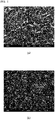
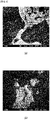
- FIG. 1(a) shows an SEM image of the structure of the ingot as observed by an electron microscope
- FIG. 1(b) shows an SEM image of the structure of the target as observed by an electron microscope
- FIGS. 2(a) and 2(b) are enlarged images of FIGS. 1(a) and 1(b) , respectively.
- the white band parts are Sc rich (AISc) parts
- the black parts are Al rich (Al 2 Sc) parts.
- a sputtering target was produced by substantially the same method as that of Example 1, with the exception that an Al raw material and a Sc raw material were mixed such that the Sc content was 30 at.%, and measured for the Sc content, contents of impurities, carbon content and oxygen content, as well as Vickers hardness, by the same methods as those of Example 1.
- the results are shown in Tables 5 to 8, respectively.
- Example 2 As shown in Table 8, in Example 2, the variation in the Vickers hardness of the target was 18.9%, which was confirmed to be 20% or less. Also in Example 2, it is understood that the variation in Vickers hardness were effectively suppressed by the forging after the melting and casting.
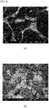
- FIG. 3(a) shows an SEM image of the structure of the ingot as observed by an electron microscope
- FIG. 3(b) shows an SEM image of the structure of the target as observed by an electron microscope
- FIGS. 4(a) and 4(b) are enlarged images of FIGS. 3(a) and 3(b) , respectively.
- the white band parts are Sc rich (Al 2 Sc) parts
- the black parts are Al rich (Al 3 Sc) parts.
- a sputtering target was produced by substantially the same method as that of Example 1, with the exception that a Sc raw material having a higher oxygen concentration was used, and measured for the Sc content, contents of impurities, carbon content and oxygen content, as well as Vickers hardness, by the same methods as those of Example 1.
- the results are shown in Tables 9 to 12, respectively.
- Example 3 As shown in Table 12, in Example 3, the variation in the Vickers hardness of the target was 6.8%, which was confirmed to be 20% or less. Also in Example 3, it is clear that the variation in the Vickers hardness was effectively suppressed by the forging after the melting and casting, as compared with the value of the variation in the Vickers hardness of the ingot.
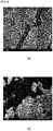
- FIG. 5(a) shows an SEM image of the structure of the ingot as observed by an electron microscope
- FIG. 5(b) shows a SEM image of the structure of the target as observed by an electron microscope
- FIGS. 6(a) and (b) are enlarged images of FIGS. 5(a) and 5(b) , respectively.
- the white band parts are Sc rich (Al 2 Sc) parts
- the black parts are Al rich (Al 3 SC) parts.
- a sputtering target having lower oxygen and a lower variation in hardness can be produced, thereby contributing to improvement of piezoelectric characteristics of a piezoelectric material formed by sputtering, and preventing cracking during the sputtering.
Description
- The present invention relates to a sputtering target which is made of an alloy of Al and Sc and which is suitable for use in forming a thin film of a piezoelectric material or the like, and to a method for producing the same. In particular, the present invention proposes a technique capable of contributing to improvement of piezoelectric characteristics of a piezoelectric material formed by sputtering.
- A filter made of a piezoelectric material, called a SAW device, is used for wireless communication devices such as mobile phones. The SAW device utilizes a surface acoustic wave (SAW) traveling on a surface of a piezoelectric material to filter unnecessary frequencies through necessary ones, and the device is widely used because it has good characteristics with lower loss and can reduce its size and thickness.
- On the other hand, in the SAW devices, a wiring width becomes narrow and a working process becomes difficult when the frequency is increased. Therefore, a film bulk acoustic resonator called an FBAR device (FBAR: Film Bulk Acoustic Resonator) is used in place of the SAW device in order to cope with a recent trend of high frequency band of electric waves. For the resonator, a piezoelectric thin film made of aluminum nitride as well as scandium aluminum nitride may be used. The piezoelectric thin film can be formed by sputtering of an aluminum alloy.
- A sputtering target for use in the sputtering for forming the piezoelectric thin film includes sputtering targets comprised of an aluminum alloy obtained by adding to aluminum at least one of copper, titanium, hafnium and palladium; or an aluminum alloy obtained by adding at least one of scandium, yttrium and lanthanoid, as described in Patent Document 1 or the like.
- Among them, the aluminum alloy containing scandium has a high piezoelectric constant and can exert good piezoelectric characteristics, particularly when the content of scandium is within a predetermined range, according to Non-patent Document 1 (particularly see
FIG. 3 ). Therefore, it is considered that the sputtering target made of the aluminum alloy containing scandium is effective for forming the above piezoelectric thin film. - Here, Patent Document 2 describes a method for producing scandium-aluminum nitride by means of sputtering on a substrate using a scandium-aluminum alloy. It also discloses that as a target used in the sputtering, metallic aluminum and metallic scandium are used as raw materials, and a SC0.42Al0.58 alloy target is produced by using a vacuum melting method.
-
- Patent Document 1:
Japanese Patent Application Publication No. 2015-96647 A - Patent Document 2:
Japanese Patent Application Publication No. 2012-12673 A - Non-Patent Document 1: Kato, et al., "Enhancement of Piezoelectric Response in Scandium Aluminum Nitride Alloy Thin Films prepared by Dual Reactive Co-Sputtering", DENSO Technical Review, DENSO Corporation, Vol. 202-207, 2012
- In order to provide the piezoelectric thin film as described above with good piezoelectric characteristics, it is necessary to reduce oxygen and carbon contained in the sputtering target for forming the thin film.
- However, since rare earth metals such as scandium are very active with oxygen, production of a sputtering target made of an alloy containing aluminum and scandium particularly by an atomizing method results in an extremely high oxygen content of about 1.0% by mass. Therefore, with the conventional sputtering target, the piezoelectric characteristics of the piezoelectric thin film could not be improved.
- In this regard, the oxygen content of the sputtering target would be able to be reduced by carrying out a melting method instead of the atomizing method as proposed in Patent Document 1.
- However, in the melting method it is not possible to select starting materials (fine particles, atomization, and the like) as in a powder method. Therefore, there is a problem that a sputtering target produced by the melting method and containing a relatively large amount of scandium results in a hardness variation over the entire target, so that cracking occurs during sputtering or the like.
- Patent Document 2 discloses that a sputtering target made of a scandium-aluminum alloy is produced by a vacuum melting method. However, with the vacuum melting method, it is difficult to uniformly control the composition of scandium. Therefore, in the vacuum melting method, any desired characteristics could not be obtained unless the target has a small diameter.
- An object of this invention is to solve such problems of the conventional sputtering targets. The object is to provide a sputtering target which can contribute to improvement of piezoelectric characteristics of a piezoelectric material formed by sputtering, while maintaining a required target hardness, and to provide a method for producing the same.
- The present inventors have focused on the fact that the oxygen content in the sputtering target can be reduced by producing the sputtering target with the melting method. As a result of extensive studies, the present inventors have obtained new findings that the hardness variation in the produced sputtering target can be significantly reduced by carrying out a predetermined melting method in an inert gas atmosphere and forging an ingot as a target material obtained by the melting method. Based on the new findings, the present inventors have found that a sputtering target can be produced which has a sufficiently low possibility of cracks when used for sputtering or the like, while reducing the oxygen content by employing the melting method.
- Based on the findings, the present invention provides a sputtering target as disclosed in claims 1-6.
- The present invention also provides a method for producing a sputtering target as disclosed in claims 7-10.
- According to the present invention, it is possible to obtain a sputtering target having a lower variation in hardness and a lower oxygen content. Thus, the sputtering target has lower possibility of cracking during sputtering and can be effectively used, and also can contribute to improvement of piezoelectric characteristics of a piezoelectric material when performing the sputtering for forming a thin film of the piezoelectric material.
-
-
FIG. 1(a) is an SEM image of a structure of an ingot according to Example 1 as observed by an electron microscope, andFIG. 1(b) is an SEM image of a structure of a target according to Example 1 as observed by an electron microscope. -
FIGS. 2 (a) and (b) are enlarged images ofFIGS. 1(a) and (b) , respectively. -
FIG. 3(a) is an SEM image of a structure of an ingot according to Example 2 as observed by an electron microscope, andFIG. 3(b) is an SEM image of a structure of a target according to Example 2 as observed by an electron microscope. -
FIGS. 4(a) and 4(b) are enlarged images ofFIGS. 3(a) and 3(b) , respectively. -
FIG. 5(a) is an SEM image of a structure of an ingot according to Example 3 as observed by an electron microscope, andFIG. 5(b) is an SEM image of a structure of a target according to Example 3 as observed by an electron microscope. -
FIG. 6(a) and 6(b) are enlarged images ofFIGS. 5(a) and 5 (b) , respectively. - Embodiments of the present invention will be described below in detail.
- A sputtering target according to one embodiment of this invention comprises an alloy of Al and Sc and contains from 25 at.% to 50 at.% of Sc. The sputtering target has an oxygen content of 2000 ppm by mass or less, and a variation in Vickers hardness of 20% or less. The sputtering target generally has a flat plate shape such as a disk, but it may also have various other shapes such as columnar shapes like a cylindrical shape.
- The sputtering target may be made of an alloy of aluminum (Al) and scandium (Sc).
- In the present invention, Sc is contained in an amount of 25 at.% or more and 50 at.% or less. According to a phase diagram, the AISc alloy in this range is composed of at least one phase of an Al-Sc phase, an Al2-Sc phase and an Al3-SC phase, and generally comprised of two phases of them. When the content of Sc is lower, the Al phase will appear. On the other hand, when the content of Sc is higher, the Al-Sc2 phase and/or the Sc phase will appear. Specifically, the content of Sc can be, for example, 25 at.% or more and less than 33 at.%, or 33 at.% or more and 50 at.% or less. According to the phase diagram, when the content of Sc is 25 at.% or more and less than 33 at.%, the AISc alloy is often comprised of the Al-Sc phase and the Al2-Sc phase, and when the content of Sc is 33 at.% or more and 50 at.% or less, the AISc alloy is often comprised of the Al2-Sc phase and the Al3-Sc phase.
- As an intermetallic compound of aluminum and scandium, the Al-Sc phase and/or Al2-Sc phase is preferably present. The presence or absence of such phases can be confirmed by X-ray diffraction (XRD) or the like.
- The sputtering target may contain, in addition to Al and Sc, at least one element selected from the group consisting of Li, Na, K, Fe, Co, and Ni as impurities excluding gas components such as oxygen, nitrogen and carbon. The total content of these elements may preferably be 0.1% by mass or less. If the content of such elements is too large, the piezoelectric characteristics are adversely affected. Therefore, the total content of the elements is preferably 0.1% by mass or less.
- The oxygen content in the sputtering target is 2000 ppm by mass or less. The lower oxygen content can be achieved by producing the target with a melting method as described below.
- When a piezoelectric material is formed by the sputtering using the sputtering target with such lower oxygen, the piezoelectric characteristics of the piezoelectric material can be effectively improved by reducing oxygen defects.
- In order to further improve the piezoelectric characteristics, the oxygen content is preferably 1500 ppm by mass or less, and more preferably 1000 ppm by mass or less, and particularly 600 ppm by mass or less, and more particularly 300 ppm by mass or less.
- A lower carbon content in the sputtering target is also preferable, in terms of improvement of the piezoelectric characteristics. This is due to generation of defects caused by carbide. Therefore, the carbon content is, for example 1000 ppm by mass or less, and preferably 500 ppm by mass or less, and more preferably 100 ppm by mass or less, and further preferably 100 ppm by mass or less, and even more preferably 50 ppm by mass or less.
- When the sputtering target is produced by a melting method in order to reduce the oxygen content as described above, a variation in Vickers hardness of the entire target will become large, which causes a problem that the sputtering target is broken during the sputtering.
- To address this problem, the variation in the Vickers hardness (Hv) of the sputtering target is set to 20% or less by carrying out a forging step as described below after the melting step during the production. Thus, any cracking during the sputtering can be effectively prevented.
- For example, in a disk-shaped sputtering target, the variation in Vickers hardness can be calculated by measuring Vickers hardness at each measurement point or the like of the total five measurement points: one point at a target central position and four points in a target outer peripheral position on the target surface, determining an average value and standard deviation of measured values at their multiple measurement points, and then dividing the standard deviation by the average value and expressing it in a percentage. It should be noted that each measurement point in the target outer peripheral position is at a distance of about 15 mm from the outer peripheral end (outer peripheral edge) of the sputtering target. For a flat sputtering target having a rectangular plate shape, the Vickers hardness is measured at the total five points: one point at the target central position and four points at a position having a distance of about 15 mm from a 1/2 (center) end of each side, and the variation is calculated from the standard deviation and average value.
- It should be noted that the Vickers hardness is measured based on a Vickers hardness test defined in JIS Z2244 (2009).
- In order to reduce any possibility of cracking during the sputtering, the variation in Vickers hardness may be 20% or less, and preferably 10% or less, and more preferably 5% or less, and further 4% or less, and more particularly 3% or less.
- The sputtering target as stated above can be produced, for example, as follows.
- First, an Al raw material and a Sc raw material are mixed together, melted in a melting furnace based on a melting method in a vacuum or an inert gas, and then cooled to obtain an ingot made of an alloy of Al and Sc as a target material. Here, the Sc raw material is added such that the Sc content is from 25 at.% to 50 at.% (25 at.% or more and less than 33 at.% ,or 33 at.% or more and 50 at.% or less). It should be noted that the cooling herein can be, for example, natural cooling which is allowed to stand in an inert gas until it reaches room temperature, although the cooling is not limited thereto. According to such a melting method, the oxygen concentration in the sputtering target produced can be sufficiently reduced, and the composition of scandium can be adjusted to be uniform, by carrying out the melting method in a vacuum or inert gas atmosphere. It should be noted that the oxygen concentration rises in the atmosphere, so it is difficult to obtain a desired ingot. It has been found that in the vacuum atmosphere, the oxygen concentration can be effectively reduced while preventing volatilization of Al and adjusting the composition, because of immediate melting and alloying with high power. The inert gas used herein may be various gases as long as they are inert gases which do not react with Al and Sc, and it may be nitrogen gas or argon gas, for example.
- In particular, the Sc raw material added herein has a lower oxygen content. Thus, the oxygen content in the sputtering target can be further reduced. Specifically, the oxygen content in the Sc raw material can be 3000 ppm by mass or less. The oxygen content in the Sc raw material may be, for example, from 100 ppm by mass to 3000 ppm by mass, and preferably from 100 ppm by mass to 2000 ppm by mass, and more preferably from 100 ppm by mass to 1000 ppm by mass. The carbon content in the Sc raw material is preferably from 10 ppm by mass to 500 ppm by mass, and more preferably from 10 ppm by mass to 100 ppm by mass.
- The ingot as described above is subjected to a forging step of applying a pressure to the ingot to subject it to plastic working, thereby producing a sputtering target having a predetermined shape. Only the melting method results in a variation in hardness of the sputtering target and tends to generate cracking during the sputtering. However, by performing the forging step, the structure can be controlled, thereby enabling production of a sputtering target which has a smaller variation in hardness and can be stably sputtered. We have studied the reason why the variation in hardness is decreased by the forging. While not wishing to be bound by any theory, it is believed that the pinning due to grain boundaries will uniformly occur wherever it is measured, and the variation will be thus reduced, because Sc rich phases (white parts as observed in a SEM photograph) were separated so as to form island shapes by the forging, for example in Example 1 described below.
- Specifically, for example, the plastic working can be performed by fixing a lower surface of a disk-shaped ingot obtained by the above melting and applying a pressure from the upper surface. Here, to suppress the variation in hardness of the sputtering target to be produced, a working rate of the plastic working in the forging step is preferably from 50% to 95%, and more preferably from 75% to 90%. If the working rate is too low, any sputtering target having Vickers hardness within a predetermined range cannot be obtained. On the other hand, if the working rate is too high, defects will be generated due to working and the defects can be starting points of cracking. The working rate is expressed as a percentage of a value calculated by the equation: (height before working - height after working) / height before working. The number of times of plastic working is not limited to one. That is, the plastic working can be carried out once or several times. For example, in the case of producing a relatively large sputtering target or the like, the plastic working may be performed several times.
- Further, since cold-forging of the Al-Sc ingot is difficult, the ingot can be press-forged while being heated at a temperature of from 500 °C to 1200 °C.
- Processing may be then performed as needed, and a backing plate for supporting the sputtering target can be bonded to one surface of the sputtering target, and the sputtering target can be subjected to finishing such as grinding. For the bonding to the backing plate, for example, brazing with a predetermined element, diffusion bonding or the like can be adopted. The bonding and processing can be carried out in the same way as the known methods.
- The sputtering target thus produced has a lower oxygen content. Therefore, when a piezoelectric material is formed by sputtering using the sputtering target, the improvement of the piezoelectric characteristics can be expected. Further, the entire sputtering target has a lower variation in Vickers hardness. Therefore, cracking can be effectively suppressed during the sputtering.
- The sputtering target according to the present invention was experimentally produced and its effects were confirmed as described below. However, the description herein is merely for the purpose of illustration and is not intended to be limited thereto.
- An Al raw material and a Sc raw material were mixed such that a Sc content was 38 at.%, and the mixture was subjected to melting at a melting point of 1150 °C by high-frequency heating in an Ar atmosphere, and a power was turned off and the mixture was left for 2 hours in the inert gas to naturally cool the mixture to produce an ingot made of an alloy of Al and Sc. Here, the carbon content in the Sc raw material was 40 ppm by mass and the oxygen content was 1400 ppm by mass. A forging step was then performed, and the ingot was subjected to one press working at a working rate of 85% while heating the ingot at 1000 °C in an Ar atmosphere, and then subjected to the required processing to form a sputtering target.
- The Sc content in the sputtering target was measured, indicating that the Sc content was as shown in Table 1, and a variation in the Sc content at each position was within a range of ± 2 at.%. Impurities contained in the sputtering target are shown in Table 2 together with their contents. In Tables 1 and 2, TOP means a top surface of the target, and BTM means a bottom surface of the target on a back side of the top surface of the target.
[Table 1] Sc Content at% Goal 38 TOP 38 BTM 36.9 [Table 2] Impurities TOP (at. ppm) BTM (at. ppm) Li < 0.01 < 0.01 Na 0.01 < 0.01 K 0.03 < 0.01 Fe 290 320 Co 10 10 Ni 160 150 - The carbon content and the oxygen content in the sputtering target were measured, indicating that measured values were as shown in Table 3. Analysis was carried out by an inert gas melting method and oxygen was detected with an infrared detector. Equipment used herein is TC 600 and TCH 600 available from LECO CORPORATION. The content was measured twice, and an average value of measured values is shown in Table 3.
- It is understood from Table 3 that the oxygen content in the produced sputtering target was effectively reduced. The carbon content and the oxygen content in the sputtering target are substantially the same as the carbon content and the oxygen content in the ingot shown in Table 3.
[Table 3] Raw Material Sc (ppm by mass) AlSc Ingot TOP (ppm by mass) AISc Ingot BTM (ppm by mass) C 40 30 30 O 1400 490 410 - Further, for each of the ingot and the sputtering target obtained by forging the ingot, the Vickers hardness was measured at total five points: one point at the central position of the ingot or the target and four points (positions of 0°, 90°, 180°, and 270°) on the outer peripheral portion of the ingot or the target, and an average value and standard deviation were calculated for each of the target or the ingot. In this case, positions of 10 mm away from the outer peripheral end of the disk-shaped ingot or target were determined to be the measurement points for the outer circumferential position of the ingot or target. The results are shown in Table 4. As can be seen from Table 4, in Example 1, the variation in the Vickers hardness of the target was 3.2%, which was confirmed to be 20% or less. It can be seen that the variation in the Vickers hardness, which was a value obtained by dividing the standard deviation by the average value and expressing it as a percentage, was effectively suppressed by the forging.
[Table 4] Vickers Hardness Hv Ingot Target Average Value 556.5 588.3 Standard Deviation 72.7 18.7 Variation (%) 13.1 3.2 FIG. 1(a) shows an SEM image of the structure of the ingot as observed by an electron microscope, andFIG. 1(b) shows an SEM image of the structure of the target as observed by an electron microscope.FIGS. 2(a) and 2(b) are enlarged images ofFIGS. 1(a) and 1(b) , respectively. In these figures, the white band parts are Sc rich (AISc) parts, and the black parts are Al rich (Al2Sc) parts. - A sputtering target was produced by substantially the same method as that of Example 1, with the exception that an Al raw material and a Sc raw material were mixed such that the Sc content was 30 at.%, and measured for the Sc content, contents of impurities, carbon content and oxygen content, as well as Vickers hardness, by the same methods as those of Example 1. The results are shown in Tables 5 to 8, respectively.
[Table 5] Sc Content at% Goal 30 TOP 29.8 BTM 31.4 [Table 6] Impurities TOP (at. ppm) BTM (at. ppm) Li < 0.01 < 0.01 Na 0.25 0.10 K 0.02 < 0.01 Fe 120 96 Co <1 <1 Ni 30 23 [Table 7] Raw Material Sc (ppm by mass) AlSc Ingot TOP (ppm by mass) AISc Ingot BTM (ppm by mass) C 80 30 <10 O 620 490 370 [Table 8] Vickers Hardness Hv Ingot Target Average Value 430.1 448.4 Standard Deviation 94.5 84.8 Variation (%) 22.0 18.9 - As shown in Table 8, in Example 2, the variation in the Vickers hardness of the target was 18.9%, which was confirmed to be 20% or less. Also in Example 2, it is understood that the variation in Vickers hardness were effectively suppressed by the forging after the melting and casting.
- In addition, for Example 2,
FIG. 3(a) shows an SEM image of the structure of the ingot as observed by an electron microscope, andFIG. 3(b) shows an SEM image of the structure of the target as observed by an electron microscope.FIGS. 4(a) and 4(b) are enlarged images ofFIGS. 3(a) and 3(b) , respectively. In the figures, the white band parts are Sc rich (Al2Sc) parts, and the black parts are Al rich (Al3Sc) parts. - A sputtering target was produced by substantially the same method as that of Example 1, with the exception that a Sc raw material having a higher oxygen concentration was used, and measured for the Sc content, contents of impurities, carbon content and oxygen content, as well as Vickers hardness, by the same methods as those of Example 1. The results are shown in Tables 9 to 12, respectively.
[Table 9] Sc Content at% Goal 38 TOP 39.9 BTM 38.7 [Table 10] Impurities TOP (at. ppm) BTM (at. ppm) Li < 0.01 < 0.01 Na < 0.01 < 0.01 K 1.1 1.4 Fe 360 370 Co <1 <1 Ni 18 17 [Table 11] Raw Material Sc (ppm by mass) AlSc Ingot TOP (ppm by mass) AlSc Ingot BTM (ppm by mass) C 200 90 80 O 2800 1920 1630 [Table 12] Vickers Hardness Hv Ingot Target Average Value 512.5 548.5 Standard Deviation 80.4 37.3 Variation (%) 15.7 6.8 - As shown in Table 12, in Example 3, the variation in the Vickers hardness of the target was 6.8%, which was confirmed to be 20% or less. Also in Example 3, it is clear that the variation in the Vickers hardness was effectively suppressed by the forging after the melting and casting, as compared with the value of the variation in the Vickers hardness of the ingot.
- For Example 3,
FIG. 5(a) shows an SEM image of the structure of the ingot as observed by an electron microscope, andFIG. 5(b) shows a SEM image of the structure of the target as observed by an electron microscope.FIGS. 6(a) and (b) are enlarged images ofFIGS. 5(a) and 5(b) , respectively. In the figures, the white band parts are Sc rich (Al2Sc) parts, and the black parts are Al rich (Al3SC) parts. - As described above, it is found that according to the present invention, a sputtering target having lower oxygen and a lower variation in hardness can be produced, thereby contributing to improvement of piezoelectric characteristics of a piezoelectric material formed by sputtering, and preventing cracking during the sputtering.
Claims (10)
- A sputtering target comprising an alloy of Al and Sc and containing from 25 at.% to 50 at.% of Sc, the sputtering target having an oxygen content of 2000 ppm by mass or less, and a variation in Vickers hardness (Hv) of 20% or less, wherein the variation in Vickers hardness (Hv) is calculated by measuring Vickers hardness at a plurality of measurement points on a target surface, determining an average value and standard deviation of measured values at the measurement points, dividing the standard deviation by the average value, and expressing in a percentage.
- The sputtering target according to claim 1, wherein the oxygen content is 1000 ppm by mass or less.
- The sputtering target according to claim 1 or 2, wherein the variation in Vickers hardness (Hv) is 5% or less.
- The sputtering target according to any one of claims 1 to 3, wherein the sputtering target has a carbon content of 1000 ppm by mass or less.
- The sputtering target according to any one of claims 1 to 4, wherein the sputtering target comprises at least one phase selected from the group consisting of an Al-Sc phase, an Al2-Sc phase and an Al3-Sc phase.
- The sputtering target according to any one of claims 1 to 5, further containing at least one element selected from the group consisting of Li, Na, K, Fe, Co and Ni in a total amount of 0.1% by mass or less.
- A method for producing a sputtering target, comprising:a melting step of melting, in an inert gas or vacuum atmosphere, an Al raw material together with a Sc raw material having an oxygen content of 3000 ppm by mass or less and then cooling to obtain an Al-Sc alloy ingot containing from 25 at.% to 50 at.% of Sc by casting; anda forging step of applying a pressure to the ingot to subject the ingot to plastic working.
- The method for producing the sputtering target according to claim 7, wherein a Sc raw material having an oxygen content of from 100 ppm by mass to 3000 ppm by mass is used in the melting step.
- The method for producing the sputtering target according to claim 7 or 8, wherein a working ratio of the plastic working in the forging step is from 50% to 95%.
- The method for producing the sputtering target according to any one of claims 7 to 9, wherein in the forging step, the ingot is subjected to plastic working while heating the ingot at a temperature of from 500 °C to 1200 °C.
Applications Claiming Priority (2)
| Application Number | Priority Date | Filing Date | Title |
|---|---|---|---|
| JP2016113945 | 2016-06-07 | ||
| PCT/JP2017/021180 WO2017213185A1 (en) | 2016-06-07 | 2017-06-07 | Sputtering target and production method therefor |
Publications (3)
| Publication Number | Publication Date |
|---|---|
| EP3467142A1 EP3467142A1 (en) | 2019-04-10 |
| EP3467142A4 EP3467142A4 (en) | 2019-12-11 |
| EP3467142B1 true EP3467142B1 (en) | 2022-08-03 |
Family
ID=60579039
Family Applications (1)
| Application Number | Title | Priority Date | Filing Date |
|---|---|---|---|
| EP17810359.4A Active EP3467142B1 (en) | 2016-06-07 | 2017-06-07 | Sputtering target and production method therefor |
Country Status (6)
| Country | Link |
|---|---|
| US (1) | US11236416B2 (en) |
| EP (1) | EP3467142B1 (en) |
| JP (1) | JP6869237B2 (en) |
| CN (1) | CN109312449B (en) |
| SG (1) | SG11201810964UA (en) |
| WO (1) | WO2017213185A1 (en) |
Families Citing this family (10)
| Publication number | Priority date | Publication date | Assignee | Title |
|---|---|---|---|---|
| US11638943B2 (en) * | 2019-04-09 | 2023-05-02 | Jin Yuncheng Enterprise Co., Ltd. | Method for manufacturing cold-forged, extruded aluminum alloy tube |
| EP4000109A1 (en) * | 2019-07-19 | 2022-05-25 | Evatec AG | Piezoelectric coating and deposition process |
| KR20220018547A (en) | 2019-07-31 | 2022-02-15 | 가부시키가이샤 후루야긴조쿠 | sputtering target |
| CN111455223B (en) * | 2019-08-08 | 2021-10-01 | 湖南稀土金属材料研究院 | Aluminum-scandium alloy target material and preparation method thereof |
| US11872616B2 (en) * | 2019-08-21 | 2024-01-16 | Jin Yuncheng Enterprise Co., Ltd. | Method for manufacturing cold-forged, extruded aluminum alloy tube |
| CN113373414B (en) * | 2020-02-25 | 2023-10-27 | 湖南东方钪业股份有限公司 | Preparation method and application of aluminum scandium alloy sputtering target |
| KR20230020509A (en) * | 2020-06-05 | 2023-02-10 | 마테리온 코포레이션 | Aluminum-scandium composite, aluminum-scandium composite sputtering target and manufacturing method |
| CN111485207A (en) * | 2020-06-08 | 2020-08-04 | 福建阿石创新材料股份有限公司 | Fine-grain homogeneous high-scandium-content aluminum-scandium alloy sintering target material and preparation method and application thereof |
| TWI744154B (en) * | 2020-12-29 | 2021-10-21 | 金允成企業股份有限公司 | Aluminum alloy rod forging and forming method |
| CN113584333B (en) * | 2021-07-14 | 2022-05-13 | 先导薄膜材料有限公司 | Method for improving uniformity of aluminum-scandium alloy target material |
Citations (10)
| Publication number | Priority date | Publication date | Assignee | Title |
|---|---|---|---|---|
| EP0855451A1 (en) | 1995-10-12 | 1998-07-29 | Kabushiki Kaisha Toshiba | Wiring film, sputter target for forming the wiring film and electronic component using the same |
| US20020083571A1 (en) | 2000-12-29 | 2002-07-04 | Solar Applied Material Technology Corp. | Method for producing metal sputtering target |
| JP2004204284A (en) | 2002-12-25 | 2004-07-22 | Toshiba Corp | Sputtering target, al alloy film, and electronic component |
| US20040140197A1 (en) | 1997-12-24 | 2004-07-22 | Kabushiki Kaisha Toshiba | Sputtering target, Al interconnection film, and electronic component |
| US20080173543A1 (en) | 2007-01-19 | 2008-07-24 | Heraeus Inc. | Low oxygen content, crack-free heusler and heusler-like alloys & deposition sources & methods of making same |
| US20110318607A1 (en) | 2009-03-02 | 2011-12-29 | Kabushiki Kaisha Kobe Seiko Sho (Kobe Steel, Ltd.) | Aluminum alloy reflective film, automobile light, illuminator, ornamentation, and aluminum alloy sputtering target |
| US20120000766A1 (en) | 2010-07-01 | 2012-01-05 | Denso Corporation | Method for manufacturing scandium aluminum nitride film |
| US20120107557A1 (en) | 2009-07-01 | 2012-05-03 | Denso Corporation | Manufacturing method of piezoelectric-body film, and piezoelectric-body film manufactured by the manufacturing method |
| JP2015096647A (en) | 2013-10-08 | 2015-05-21 | 株式会社フルヤ金属 | Alloy target of aluminum and rare earth element and manufacturing method of the same |
| CN104805406A (en) | 2015-04-17 | 2015-07-29 | 无锡舒玛天科新能源技术有限公司 | Aluminium-scandium rotating target material and preparation method thereof |
Family Cites Families (20)
| Publication number | Priority date | Publication date | Assignee | Title |
|---|---|---|---|---|
| JPH02115364A (en) | 1988-10-22 | 1990-04-27 | Dowa Mining Co Ltd | Tellurium target and production thereof |
| JP3560393B2 (en) * | 1995-07-06 | 2004-09-02 | 株式会社日鉱マテリアルズ | Manufacturing method of aluminum alloy sputtering target |
| JP3365954B2 (en) * | 1997-04-14 | 2003-01-14 | 株式会社神戸製鋼所 | Al-Ni-Y alloy thin film for semiconductor electrode and sputtering target for forming Al-Ni-Y alloy thin film for semiconductor electrode |
| US6250362B1 (en) * | 1998-03-02 | 2001-06-26 | Alcoa Inc. | Method and apparatus for producing a porous metal via spray casting |
| US6135198A (en) * | 1998-03-05 | 2000-10-24 | Aluminum Company Of America | Substrate system for spray forming |
| JP2001230116A (en) * | 1999-12-09 | 2001-08-24 | Sumitomo Electric Ind Ltd | Electromagnetic actuator |
| JP5038553B2 (en) | 2000-04-27 | 2012-10-03 | 株式会社東芝 | Manufacturing method of sputtering target |
| JP2003046250A (en) | 2001-02-28 | 2003-02-14 | Furukawa Electric Co Ltd:The | Multilayer substrate with via for build-up and its manufacturing method |
| WO2003046250A1 (en) | 2001-11-26 | 2003-06-05 | Nikko Materials Company, Limited | Sputtering target and production method therefor |
| JP3898043B2 (en) | 2001-11-30 | 2007-03-28 | 株式会社東芝 | Sputtering target and semiconductor device and sputtering apparatus using the same |
| JP4997448B2 (en) * | 2007-12-21 | 2012-08-08 | 独立行政法人産業技術総合研究所 | Nitride semiconductor manufacturing method and nitride semiconductor device |
| TW201040050A (en) | 2009-05-11 | 2010-11-16 | Univ Nat Central | Aluminum scandium alloy film for use in vehicle lamp and production method thereof |
| CN101924023A (en) | 2009-06-09 | 2010-12-22 | 日本派欧尼株式会社 | The epitaxially growing equipment of III group-III nitride semiconductor |
| KR101273021B1 (en) | 2009-08-12 | 2013-06-10 | 가부시키가이샤 아루박 | Sputtering target and method for manufacturing a sputtering target |
| JP5681368B2 (en) | 2010-02-26 | 2015-03-04 | 株式会社神戸製鋼所 | Al-based alloy sputtering target |
| US20140174908A1 (en) | 2011-03-29 | 2014-06-26 | Avago Technologies General Ip (Singapore) Pte. Ltd. | Scandium-aluminum alloy sputtering targets |
| JP5817673B2 (en) | 2011-11-18 | 2015-11-18 | 株式会社村田製作所 | Piezoelectric thin film resonator and method for manufacturing piezoelectric thin film |
| CA2773197A1 (en) * | 2012-03-27 | 2013-09-27 | Yundong Li | Electroplated super abrasive tools with the abrasive particles chemically bonded and deliberately placed, and methods for making the same |
| AU2013201572B2 (en) * | 2013-03-15 | 2014-12-11 | Commonwealth Scientific And Industrial Research Organisation | Production of Aluminium-Scandium Alloys |
| JP5966199B2 (en) | 2013-05-31 | 2016-08-10 | 株式会社デンソー | Piezoelectric thin film and manufacturing method thereof |
-
2017
- 2017-06-07 WO PCT/JP2017/021180 patent/WO2017213185A1/en unknown
- 2017-06-07 CN CN201780035628.7A patent/CN109312449B/en active Active
- 2017-06-07 SG SG11201810964UA patent/SG11201810964UA/en unknown
- 2017-06-07 US US16/307,521 patent/US11236416B2/en active Active
- 2017-06-07 JP JP2018521760A patent/JP6869237B2/en active Active
- 2017-06-07 EP EP17810359.4A patent/EP3467142B1/en active Active
Patent Citations (10)
| Publication number | Priority date | Publication date | Assignee | Title |
|---|---|---|---|---|
| EP0855451A1 (en) | 1995-10-12 | 1998-07-29 | Kabushiki Kaisha Toshiba | Wiring film, sputter target for forming the wiring film and electronic component using the same |
| US20040140197A1 (en) | 1997-12-24 | 2004-07-22 | Kabushiki Kaisha Toshiba | Sputtering target, Al interconnection film, and electronic component |
| US20020083571A1 (en) | 2000-12-29 | 2002-07-04 | Solar Applied Material Technology Corp. | Method for producing metal sputtering target |
| JP2004204284A (en) | 2002-12-25 | 2004-07-22 | Toshiba Corp | Sputtering target, al alloy film, and electronic component |
| US20080173543A1 (en) | 2007-01-19 | 2008-07-24 | Heraeus Inc. | Low oxygen content, crack-free heusler and heusler-like alloys & deposition sources & methods of making same |
| US20110318607A1 (en) | 2009-03-02 | 2011-12-29 | Kabushiki Kaisha Kobe Seiko Sho (Kobe Steel, Ltd.) | Aluminum alloy reflective film, automobile light, illuminator, ornamentation, and aluminum alloy sputtering target |
| US20120107557A1 (en) | 2009-07-01 | 2012-05-03 | Denso Corporation | Manufacturing method of piezoelectric-body film, and piezoelectric-body film manufactured by the manufacturing method |
| US20120000766A1 (en) | 2010-07-01 | 2012-01-05 | Denso Corporation | Method for manufacturing scandium aluminum nitride film |
| JP2015096647A (en) | 2013-10-08 | 2015-05-21 | 株式会社フルヤ金属 | Alloy target of aluminum and rare earth element and manufacturing method of the same |
| CN104805406A (en) | 2015-04-17 | 2015-07-29 | 无锡舒玛天科新能源技术有限公司 | Aluminium-scandium rotating target material and preparation method thereof |
Non-Patent Citations (7)
| Title |
|---|
| AKIYAMA MORITO ET AL: "Influence of oxygen concentration in sputtering gas on piezoelectric response of aluminum nitride thin films", APPLIED PHYSICS LETTERS, vol. 93, no. 2, 14 July 2008 (2008-07-14), 2 Huntington Quadrangle, Melville, NY 11747, pages 021903 - 021903-3, XP012112414, ISSN: 0003-6951, DOI: 10.1063/1.2957654 |
| ANONYMOUS: "JIS Z 2244 (JISF) Vickers hardness test - Test method", JIS JAPANESE INDUSTRIAL STANDARD, 1 January 2009 (2009-01-01), pages 1 - 115, XP093047697 |
| J. ROYSET ET AL.: "Scandium in aluminium alloy s", INT. MAT. REV., vol. 50, 2005, pages 19 - 44, XP008065171 |
| K. KANO ET AL.: "Enhancement of Piezoelectric Response in Scandium Aluminum Nitride Alloy Thin Films prepared by Dual Reactive Co-Sputtering", DENSO TECHNICAL REVIEW, vol. 17, 2012, pages 202 - 207, XP093047711 |
| M. AKIYAMA ET AL.: "Preparation of scandium aluminum nitride thin films using scandium aluminum alloy sputtering target and design of experiments", J. CERAM. SOC. JPN., vol. 118, no. 12, 2010, pages 1166 - 1169, XP055724685, DOI: 10.2109/jcersj2.118.1166 |
| M. SUZUKI ET AL.: "Polarity-inverted ScAIN film growth by ion beam irradiation and application to overtone acoustic wave (000-1)/(0001) film resonators", APPL. PHYS. LETT., vol. 104, 2014, pages 172905, XP012185143, DOI: 10.1063/1.4874840 |
| MASAHIRO SUMISAKA ET AL: "Sputter deposition of ScAlN using large size alloy target with high Sc content and reduction of Sc content in deposited films", JAPANESE JOURNAL OF APPLIED PHYSICS, vol. 54, no. 7S1, 1 July 2015 (2015-07-01), JP , pages 07HD06, XP055483117, ISSN: 0021-4922, DOI: 10.7567/JJAP.54.07HD06 |
Also Published As
| Publication number | Publication date |
|---|---|
| CN109312449A (en) | 2019-02-05 |
| JPWO2017213185A1 (en) | 2019-04-04 |
| US11236416B2 (en) | 2022-02-01 |
| WO2017213185A1 (en) | 2017-12-14 |
| CN109312449B (en) | 2022-04-12 |
| SG11201810964UA (en) | 2019-01-30 |
| JP6869237B2 (en) | 2021-05-12 |
| EP3467142A1 (en) | 2019-04-10 |
| EP3467142A4 (en) | 2019-12-11 |
| US20190161851A1 (en) | 2019-05-30 |
Similar Documents
| Publication | Publication Date | Title |
|---|---|---|
| EP3467142B1 (en) | Sputtering target and production method therefor | |
| KR102519021B1 (en) | Tungsten silicide target and method of manufacturing same | |
| JP2009074127A (en) | Sintered sputtering target material and manufacturing method therefor | |
| WO2015127613A1 (en) | High-purity tantalum powder and preparation method therefor | |
| US9689067B2 (en) | Method for producing molybdenum target | |
| US20090280025A1 (en) | High-Purity Ru Alloy Target, Process for Producing the Same, and Sputtered Film | |
| EP3124647B1 (en) | Sputtering target comprising al-te-cu-zr alloy, and method for producing same | |
| TWI519648B (en) | Ti-Al alloy sputtering target | |
| WO2021019992A1 (en) | Sputtering target | |
| JP7203065B2 (en) | sputtering target | |
| JP7203064B2 (en) | sputtering target | |
| WO2021241522A1 (en) | METAL-Si BASED POWDER, METHOD FOR PRODUCING SAME, METAL-Si BASED SINTERED BODY, SPUTTERING TARGET, AND METAL-Si BASED THIN FILM MANUFACTURING METHOD | |
| JP2022044768A (en) | Sputtering target | |
| JP2021152203A (en) | Sputtering target | |
| EP3170916B1 (en) | Sputterring target comprising al-te-cu-zr-based alloy and method of manufacturing the same | |
| TW202113096A (en) | Sputtering target | |
| WO2020066114A1 (en) | Sputtering target and powder for producing sputtering target | |
| JP2021088755A (en) | Sputtering target | |
| KR20230133222A (en) | Chromium sintered body, method of manufacturing the same, sputtering target, and method of manufacturing substrate with chromium film | |
| EP3569731A1 (en) | Cr alloy target material | |
| JP2021025129A (en) | Sputtering target |
Legal Events
| Date | Code | Title | Description |
|---|---|---|---|
| STAA | Information on the status of an ep patent application or granted ep patent |
Free format text: STATUS: THE INTERNATIONAL PUBLICATION HAS BEEN MADE |
|
| PUAI | Public reference made under article 153(3) epc to a published international application that has entered the european phase |
Free format text: ORIGINAL CODE: 0009012 |
|
| STAA | Information on the status of an ep patent application or granted ep patent |
Free format text: STATUS: REQUEST FOR EXAMINATION WAS MADE |
|
| 17P | Request for examination filed |
Effective date: 20181211 |
|
| AK | Designated contracting states |
Kind code of ref document: A1 Designated state(s): AL AT BE BG CH CY CZ DE DK EE ES FI FR GB GR HR HU IE IS IT LI LT LU LV MC MK MT NL NO PL PT RO RS SE SI SK SM TR |
|
| AX | Request for extension of the european patent |
Extension state: BA ME |
|
| STAA | Information on the status of an ep patent application or granted ep patent |
Free format text: STATUS: REQUEST FOR EXAMINATION WAS MADE |
|
| DAV | Request for validation of the european patent (deleted) | ||
| DAX | Request for extension of the european patent (deleted) | ||
| A4 | Supplementary search report drawn up and despatched |
Effective date: 20191108 |
|
| RIC1 | Information provided on ipc code assigned before grant |
Ipc: C22F 1/04 20060101ALI20191104BHEP Ipc: C22F 1/00 20060101ALI20191104BHEP Ipc: C22F 1/16 20060101ALI20191104BHEP Ipc: C23C 14/34 20060101AFI20191104BHEP Ipc: C22C 21/00 20060101ALI20191104BHEP Ipc: C22C 28/00 20060101ALI20191104BHEP |
|
| RIC1 | Information provided on ipc code assigned before grant |
Ipc: C23C 14/34 20060101AFI20220302BHEP |
|
| GRAP | Despatch of communication of intention to grant a patent |
Free format text: ORIGINAL CODE: EPIDOSNIGR1 |
|
| STAA | Information on the status of an ep patent application or granted ep patent |
Free format text: STATUS: GRANT OF PATENT IS INTENDED |
|
| INTG | Intention to grant announced |
Effective date: 20220412 |
|
| GRAS | Grant fee paid |
Free format text: ORIGINAL CODE: EPIDOSNIGR3 |
|
| GRAA | (expected) grant |
Free format text: ORIGINAL CODE: 0009210 |
|
| STAA | Information on the status of an ep patent application or granted ep patent |
Free format text: STATUS: THE PATENT HAS BEEN GRANTED |
|
| RAP3 | Party data changed (applicant data changed or rights of an application transferred) |
Owner name: JX NIPPON MINING & METALS CORPORATION |
|
| AK | Designated contracting states |
Kind code of ref document: B1 Designated state(s): AL AT BE BG CH CY CZ DE DK EE ES FI FR GB GR HR HU IE IS IT LI LT LU LV MC MK MT NL NO PL PT RO RS SE SI SK SM TR |
|
| REG | Reference to a national code |
Ref country code: AT Ref legal event code: REF Ref document number: 1508813 Country of ref document: AT Kind code of ref document: T Effective date: 20220815 Ref country code: CH Ref legal event code: EP |
|
| REG | Reference to a national code |
Ref country code: DE Ref legal event code: R096 Ref document number: 602017060265 Country of ref document: DE |
|
| REG | Reference to a national code |
Ref country code: IE Ref legal event code: FG4D |
|
| REG | Reference to a national code |
Ref country code: LT Ref legal event code: MG9D |
|
| REG | Reference to a national code |
Ref country code: NL Ref legal event code: MP Effective date: 20220803 |
|
| PG25 | Lapsed in a contracting state [announced via postgrant information from national office to epo] |
Ref country code: SE Free format text: LAPSE BECAUSE OF FAILURE TO SUBMIT A TRANSLATION OF THE DESCRIPTION OR TO PAY THE FEE WITHIN THE PRESCRIBED TIME-LIMIT Effective date: 20220803 Ref country code: RS Free format text: LAPSE BECAUSE OF FAILURE TO SUBMIT A TRANSLATION OF THE DESCRIPTION OR TO PAY THE FEE WITHIN THE PRESCRIBED TIME-LIMIT Effective date: 20220803 Ref country code: PT Free format text: LAPSE BECAUSE OF FAILURE TO SUBMIT A TRANSLATION OF THE DESCRIPTION OR TO PAY THE FEE WITHIN THE PRESCRIBED TIME-LIMIT Effective date: 20221205 Ref country code: NO Free format text: LAPSE BECAUSE OF FAILURE TO SUBMIT A TRANSLATION OF THE DESCRIPTION OR TO PAY THE FEE WITHIN THE PRESCRIBED TIME-LIMIT Effective date: 20221103 Ref country code: NL Free format text: LAPSE BECAUSE OF FAILURE TO SUBMIT A TRANSLATION OF THE DESCRIPTION OR TO PAY THE FEE WITHIN THE PRESCRIBED TIME-LIMIT Effective date: 20220803 Ref country code: LV Free format text: LAPSE BECAUSE OF FAILURE TO SUBMIT A TRANSLATION OF THE DESCRIPTION OR TO PAY THE FEE WITHIN THE PRESCRIBED TIME-LIMIT Effective date: 20220803 Ref country code: LT Free format text: LAPSE BECAUSE OF FAILURE TO SUBMIT A TRANSLATION OF THE DESCRIPTION OR TO PAY THE FEE WITHIN THE PRESCRIBED TIME-LIMIT Effective date: 20220803 Ref country code: FI Free format text: LAPSE BECAUSE OF FAILURE TO SUBMIT A TRANSLATION OF THE DESCRIPTION OR TO PAY THE FEE WITHIN THE PRESCRIBED TIME-LIMIT Effective date: 20220803 Ref country code: ES Free format text: LAPSE BECAUSE OF FAILURE TO SUBMIT A TRANSLATION OF THE DESCRIPTION OR TO PAY THE FEE WITHIN THE PRESCRIBED TIME-LIMIT Effective date: 20220803 |
|
| REG | Reference to a national code |
Ref country code: AT Ref legal event code: MK05 Ref document number: 1508813 Country of ref document: AT Kind code of ref document: T Effective date: 20220803 |
|
| PG25 | Lapsed in a contracting state [announced via postgrant information from national office to epo] |
Ref country code: PL Free format text: LAPSE BECAUSE OF FAILURE TO SUBMIT A TRANSLATION OF THE DESCRIPTION OR TO PAY THE FEE WITHIN THE PRESCRIBED TIME-LIMIT Effective date: 20220803 Ref country code: IS Free format text: LAPSE BECAUSE OF FAILURE TO SUBMIT A TRANSLATION OF THE DESCRIPTION OR TO PAY THE FEE WITHIN THE PRESCRIBED TIME-LIMIT Effective date: 20221203 Ref country code: HR Free format text: LAPSE BECAUSE OF FAILURE TO SUBMIT A TRANSLATION OF THE DESCRIPTION OR TO PAY THE FEE WITHIN THE PRESCRIBED TIME-LIMIT Effective date: 20220803 Ref country code: GR Free format text: LAPSE BECAUSE OF FAILURE TO SUBMIT A TRANSLATION OF THE DESCRIPTION OR TO PAY THE FEE WITHIN THE PRESCRIBED TIME-LIMIT Effective date: 20221104 |
|
| PG25 | Lapsed in a contracting state [announced via postgrant information from national office to epo] |
Ref country code: SM Free format text: LAPSE BECAUSE OF FAILURE TO SUBMIT A TRANSLATION OF THE DESCRIPTION OR TO PAY THE FEE WITHIN THE PRESCRIBED TIME-LIMIT Effective date: 20220803 Ref country code: RO Free format text: LAPSE BECAUSE OF FAILURE TO SUBMIT A TRANSLATION OF THE DESCRIPTION OR TO PAY THE FEE WITHIN THE PRESCRIBED TIME-LIMIT Effective date: 20220803 Ref country code: DK Free format text: LAPSE BECAUSE OF FAILURE TO SUBMIT A TRANSLATION OF THE DESCRIPTION OR TO PAY THE FEE WITHIN THE PRESCRIBED TIME-LIMIT Effective date: 20220803 Ref country code: CZ Free format text: LAPSE BECAUSE OF FAILURE TO SUBMIT A TRANSLATION OF THE DESCRIPTION OR TO PAY THE FEE WITHIN THE PRESCRIBED TIME-LIMIT Effective date: 20220803 Ref country code: AT Free format text: LAPSE BECAUSE OF FAILURE TO SUBMIT A TRANSLATION OF THE DESCRIPTION OR TO PAY THE FEE WITHIN THE PRESCRIBED TIME-LIMIT Effective date: 20220803 |
|
| REG | Reference to a national code |
Ref country code: DE Ref legal event code: R026 Ref document number: 602017060265 Country of ref document: DE |
|
| PLBI | Opposition filed |
Free format text: ORIGINAL CODE: 0009260 |
|
| PLAX | Notice of opposition and request to file observation + time limit sent |
Free format text: ORIGINAL CODE: EPIDOSNOBS2 |
|
| PG25 | Lapsed in a contracting state [announced via postgrant information from national office to epo] |
Ref country code: SK Free format text: LAPSE BECAUSE OF FAILURE TO SUBMIT A TRANSLATION OF THE DESCRIPTION OR TO PAY THE FEE WITHIN THE PRESCRIBED TIME-LIMIT Effective date: 20220803 Ref country code: EE Free format text: LAPSE BECAUSE OF FAILURE TO SUBMIT A TRANSLATION OF THE DESCRIPTION OR TO PAY THE FEE WITHIN THE PRESCRIBED TIME-LIMIT Effective date: 20220803 |
|
| 26 | Opposition filed |
Opponent name: MATERION CORPORATION Effective date: 20230502 |
|
| P01 | Opt-out of the competence of the unified patent court (upc) registered |
Effective date: 20230428 |
|
| PG25 | Lapsed in a contracting state [announced via postgrant information from national office to epo] |
Ref country code: AL Free format text: LAPSE BECAUSE OF FAILURE TO SUBMIT A TRANSLATION OF THE DESCRIPTION OR TO PAY THE FEE WITHIN THE PRESCRIBED TIME-LIMIT Effective date: 20220803 |
|
| PGFP | Annual fee paid to national office [announced via postgrant information from national office to epo] |
Ref country code: IT Payment date: 20230526 Year of fee payment: 7 Ref country code: FR Payment date: 20230523 Year of fee payment: 7 Ref country code: DE Payment date: 20230516 Year of fee payment: 7 |
|
| PG25 | Lapsed in a contracting state [announced via postgrant information from national office to epo] |
Ref country code: SI Free format text: LAPSE BECAUSE OF FAILURE TO SUBMIT A TRANSLATION OF THE DESCRIPTION OR TO PAY THE FEE WITHIN THE PRESCRIBED TIME-LIMIT Effective date: 20220803 |
|
| PGFP | Annual fee paid to national office [announced via postgrant information from national office to epo] |
Ref country code: BE Payment date: 20230517 Year of fee payment: 7 |
|
| PLBB | Reply of patent proprietor to notice(s) of opposition received |
Free format text: ORIGINAL CODE: EPIDOSNOBS3 |
|
| RAP4 | Party data changed (patent owner data changed or rights of a patent transferred) |
Owner name: JX METALS CORPORATION |
|
| PGFP | Annual fee paid to national office [announced via postgrant information from national office to epo] |
Ref country code: GB Payment date: 20230518 Year of fee payment: 7 Ref country code: CH Payment date: 20230702 Year of fee payment: 7 |
|
| PG25 | Lapsed in a contracting state [announced via postgrant information from national office to epo] |
Ref country code: MC Free format text: LAPSE BECAUSE OF FAILURE TO SUBMIT A TRANSLATION OF THE DESCRIPTION OR TO PAY THE FEE WITHIN THE PRESCRIBED TIME-LIMIT Effective date: 20220803 |
|
| PG25 | Lapsed in a contracting state [announced via postgrant information from national office to epo] |
Ref country code: MC Free format text: LAPSE BECAUSE OF FAILURE TO SUBMIT A TRANSLATION OF THE DESCRIPTION OR TO PAY THE FEE WITHIN THE PRESCRIBED TIME-LIMIT Effective date: 20220803 |
|
| PG25 | Lapsed in a contracting state [announced via postgrant information from national office to epo] |
Ref country code: LU Free format text: LAPSE BECAUSE OF NON-PAYMENT OF DUE FEES Effective date: 20230607 |
|
| REG | Reference to a national code |
Ref country code: IE Ref legal event code: MM4A |
|
| PG25 | Lapsed in a contracting state [announced via postgrant information from national office to epo] |
Ref country code: LU Free format text: LAPSE BECAUSE OF NON-PAYMENT OF DUE FEES Effective date: 20230607 |