WO2011105326A1 - 接合装置 - Google Patents
接合装置 Download PDFInfo
- Publication number
- WO2011105326A1 WO2011105326A1 PCT/JP2011/053674 JP2011053674W WO2011105326A1 WO 2011105326 A1 WO2011105326 A1 WO 2011105326A1 JP 2011053674 W JP2011053674 W JP 2011053674W WO 2011105326 A1 WO2011105326 A1 WO 2011105326A1
- Authority
- WO
- WIPO (PCT)
- Prior art keywords
- substrate
- wafer
- holding member
- joining device
- chuck
- Prior art date
- Legal status (The legal status is an assumption and is not a legal conclusion. Google has not performed a legal analysis and makes no representation as to the accuracy of the status listed.)
- Ceased
Links
Images






Classifications
-
- H—ELECTRICITY
- H10—SEMICONDUCTOR DEVICES; ELECTRIC SOLID-STATE DEVICES NOT OTHERWISE PROVIDED FOR
- H10D—INORGANIC ELECTRIC SEMICONDUCTOR DEVICES
- H10D86/00—Integrated devices formed in or on insulating or conducting substrates, e.g. formed in silicon-on-insulator [SOI] substrates or on stainless steel or glass substrates
-
- H—ELECTRICITY
- H10—SEMICONDUCTOR DEVICES; ELECTRIC SOLID-STATE DEVICES NOT OTHERWISE PROVIDED FOR
- H10P—GENERIC PROCESSES OR APPARATUS FOR THE MANUFACTURE OR TREATMENT OF DEVICES COVERED BY CLASS H10
- H10P72/00—Handling or holding of wafers, substrates or devices during manufacture or treatment thereof
- H10P72/04—Apparatus for manufacture or treatment
- H10P72/0428—Apparatus for mechanical treatment or grinding or cutting
-
- H—ELECTRICITY
- H10—SEMICONDUCTOR DEVICES; ELECTRIC SOLID-STATE DEVICES NOT OTHERWISE PROVIDED FOR
- H10P—GENERIC PROCESSES OR APPARATUS FOR THE MANUFACTURE OR TREATMENT OF DEVICES COVERED BY CLASS H10
- H10P10/00—Bonding of wafers, substrates or parts of devices
- H10P10/12—Bonding of semiconductor wafers or semiconductor substrates to semiconductor wafers or semiconductor substrates
- H10P10/128—Bonding of semiconductor wafers or semiconductor substrates to semiconductor wafers or semiconductor substrates by direct semiconductor to semiconductor bonding
-
- H—ELECTRICITY
- H10—SEMICONDUCTOR DEVICES; ELECTRIC SOLID-STATE DEVICES NOT OTHERWISE PROVIDED FOR
- H10P—GENERIC PROCESSES OR APPARATUS FOR THE MANUFACTURE OR TREATMENT OF DEVICES COVERED BY CLASS H10
- H10P95/00—Generic processes or apparatus for manufacture or treatments not covered by the other groups of this subclass
-
- Y—GENERAL TAGGING OF NEW TECHNOLOGICAL DEVELOPMENTS; GENERAL TAGGING OF CROSS-SECTIONAL TECHNOLOGIES SPANNING OVER SEVERAL SECTIONS OF THE IPC; TECHNICAL SUBJECTS COVERED BY FORMER USPC CROSS-REFERENCE ART COLLECTIONS [XRACs] AND DIGESTS
- Y10—TECHNICAL SUBJECTS COVERED BY FORMER USPC
- Y10T—TECHNICAL SUBJECTS COVERED BY FORMER US CLASSIFICATION
- Y10T29/00—Metal working
- Y10T29/53—Means to assemble or disassemble
- Y10T29/53087—Means to assemble or disassemble with signal, scale, illuminator, or optical viewer
- Y10T29/53091—Means to assemble or disassemble with signal, scale, illuminator, or optical viewer for work-holder for assembly or disassembly
-
- Y—GENERAL TAGGING OF NEW TECHNOLOGICAL DEVELOPMENTS; GENERAL TAGGING OF CROSS-SECTIONAL TECHNOLOGIES SPANNING OVER SEVERAL SECTIONS OF THE IPC; TECHNICAL SUBJECTS COVERED BY FORMER USPC CROSS-REFERENCE ART COLLECTIONS [XRACs] AND DIGESTS
- Y10—TECHNICAL SUBJECTS COVERED BY FORMER USPC
- Y10T—TECHNICAL SUBJECTS COVERED BY FORMER US CLASSIFICATION
- Y10T29/00—Metal working
- Y10T29/53—Means to assemble or disassemble
- Y10T29/53096—Means to assemble or disassemble including means to provide a controlled environment
-
- Y—GENERAL TAGGING OF NEW TECHNOLOGICAL DEVELOPMENTS; GENERAL TAGGING OF CROSS-SECTIONAL TECHNOLOGIES SPANNING OVER SEVERAL SECTIONS OF THE IPC; TECHNICAL SUBJECTS COVERED BY FORMER USPC CROSS-REFERENCE ART COLLECTIONS [XRACs] AND DIGESTS
- Y10—TECHNICAL SUBJECTS COVERED BY FORMER USPC
- Y10T—TECHNICAL SUBJECTS COVERED BY FORMER US CLASSIFICATION
- Y10T29/00—Metal working
- Y10T29/53—Means to assemble or disassemble
- Y10T29/5313—Means to assemble electrical device
- Y10T29/5317—Laminated device
Definitions
- the present invention relates to a bonding apparatus for bonding substrates together.
- the bonding apparatus includes a chamber that accommodates two wafers in a vertically arranged state (hereinafter, the upper wafer is referred to as an “upper wafer” and the lower wafer is referred to as a “lower wafer”), And a push pin that presses the center portion of the upper wafer, and a spacer that supports the outer periphery of the upper wafer and can be retracted from the outer periphery of the upper wafer.
- the wafers are bonded to each other in a vacuum atmosphere in order to suppress the generation of voids between the wafers. Specifically, first, in a state where the upper wafer is supported by the spacer, the central portion of the upper wafer is pressed by the push pin, and the central portion is brought into contact with the lower wafer. Thereafter, the spacer supporting the upper wafer is retracted, and the entire surface of the upper wafer is brought into contact with the entire surface of the lower wafer and bonded together (Patent Document 1).
- the present invention has been made in view of such a point, and an object thereof is to appropriately and efficiently join substrates together while suppressing generation of voids between the substrates.
- the present invention is a bonding apparatus for bonding substrates, the first holding member for mounting and holding the first substrate on the upper surface, and the first holding member.
- a second holding member that is provided above the first holding member and holds the second substrate on the lower surface, and one end of the first substrate at the time of joining the first substrate and the second substrate
- a pressing member that contacts and presses one end of the second substrate facing the one end of the first substrate, a reversing mechanism that reverses the front and back surfaces of the second substrate, and the bonding
- a transport mechanism for transporting the first substrate, the second substrate, or the superposed substrate in the apparatus.
- the first substrate is first held by the first holding member, and then the front and back surfaces of the second substrate are reversed by the reversing mechanism, and then the second substrate is the second holding member. Retained. Thereafter, the first substrate and the second substrate are arranged to face each other at a predetermined interval, and the one end portion of the first substrate and the one end portion of the second substrate are brought into contact with each other and pressed by the pushing member. Then, in a state where one end of the first substrate and one end of the second substrate are pressed, the second substrate is moved from the one end to the other end of the second substrate. The first substrate and the second substrate can be joined by sequentially contacting the substrates.
- the air is always outside the portion where the second substrate is in contact with the first substrate, that is, It exists in the other end side, and the air can be released in one direction from between the substrates. Therefore, according to the present invention, it is possible to appropriately bond the substrates while suppressing generation of voids between the substrates. Moreover, according to the present invention, it is not necessary to use a vacuum atmosphere when bonding the substrates as in the prior art, so that the substrates can be bonded efficiently in a short time, and the throughput of the substrate bonding process is improved. Can be made. Furthermore, according to the present invention, the first substrate can be brought into contact with one end of the substrate while the second substrate is held by the second holding member. The position of the second substrate with respect to the other substrate is not shifted, and the substrates can be bonded appropriately.
- the second holding member evacuates and holds the second substrate by vacuuming, and the second holding member is partitioned into a plurality of regions, and evacuation of the second substrate can be set for each region. There may be.
- the pressure in the joining device may be positive with respect to the external pressure.
- At least the first holding member or the second holding member may have a cooling mechanism for cooling at least the first substrate or the second substrate.
- a position adjusting mechanism for adjusting a horizontal direction of the first substrate or the second substrate, and the reversing mechanism is movable between the position adjusting mechanism and the second holding member. Good.
- the first substrate, the second substrate or the superposed substrate In order to carry in and out the first substrate, the second substrate or the superposed substrate from outside, the first substrate, the second substrate or the superposed substrate has a transition for temporarily placing the first substrate, the second substrate or the superposed substrate. Also good.
- the other end of the second substrate may be supported and movable in the horizontal direction.
- the imaging member and a second imaging member that images the surface of the second substrate, and the moving mechanism includes a reference point of the first substrate in an image captured by the first imaging member;
- the relative horizontal position of the first holding member and the second holding member is adjusted so that the reference point of the second substrate in the image captured by the second imaging member matches. May be.
- the surface of the substrate refers to a bonding surface to which the substrate is bonded.
- the present invention it is possible to appropriately and efficiently bond the substrates together while suppressing the generation of voids between the substrates.
- FIG. 1 is a plan view showing an outline of a configuration of a joining system 1 including a joining apparatus according to the present embodiment.
- FIG. 2 is a side view illustrating the outline of the internal configuration of the joining system 1.
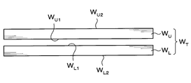
- the wafer disposed on the upper side is referred to as “upper wafer W U ” as the second substrate
- the wafer disposed on the lower side is referred to as “lower wafer W L ” as the first substrate.
- a bonding surface to which the upper wafer W U is bonded is referred to as “front surface W U1 ”
- a surface opposite to the front surface W U1 is referred to as “back surface W U2 ”.
- the bonding surface to which the lower wafer W L is bonded is referred to as “front surface W L1 ”, and the surface opposite to the front surface W L1 is referred to as “back surface WL 2 ”. Then, in the bonding system 1, by joining the upper wafer W U and the lower wafer W L, to form the overlapped wafer W T as a polymerization substrate.
- the bonding system 1 carries in and out cassettes C U , C L , and C T that can accommodate a plurality of wafers W U and W L and a plurality of superposed wafers W T , respectively, with the outside.
- the loading / unloading station 2 and the processing station 3 including various processing apparatuses that perform predetermined processing on the wafers W U , W L , and the overlapped wafer W T are integrally connected.
- the loading / unloading station 2 is provided with a cassette mounting table 10.
- the cassette mounting table 10 is provided with a plurality of, for example, four cassette mounting plates 11.
- the cassette mounting plates 11 are arranged in a line in the horizontal X direction (vertical direction in FIG. 1). These cassette mounting plates 11, cassettes C U to the outside of the interface system 1, C L, when loading and unloading the C T, a cassette C U, C L, it is possible to place the C T .
- carry-out station 2 a wafer over multiple W U, a plurality of lower wafer W L, and is configured to be held by a plurality of overlapped wafer W T.
- the number of cassette mounting plates 11 is not limited to the present embodiment, and can be arbitrarily determined.
- One of the cassettes may be used for collecting defective wafers. That is a cassette a wafer caused a problem with the bonding of the upper wafer W U and the lower wafer W L, it can be separated from the other normal overlapped wafer W T by various factors.
- a cassette a wafer caused a problem with the bonding of the upper wafer W U and the lower wafer W L, it can be separated from the other normal overlapped wafer W T by various factors.
- using a one cassette C T for the recovery of the fault wafer, and using other cassettes C T for the accommodation of a normal overlapped wafer W T are examples of the cassettes C T.
- a wafer transfer unit 20 is provided adjacent to the cassette mounting table 10.
- the wafer transfer unit 20 is provided with a wafer transfer device 22 that is movable on a transfer path 21 extending in the X direction.
- the wafer transfer device 22 is also movable in the vertical direction and around the vertical axis ( ⁇ direction), and includes cassettes C U , C L , C T on each cassette mounting plate 11 and a third of the processing station 3 described later.
- the wafers W U and W L and the superposed wafer W T can be transferred between the transition devices 50 and 51 in the processing block G3.
- the processing station 3 is provided with a plurality of, for example, three processing blocks G1, G2, G3 provided with various devices.
- a first processing block G1 is provided on the front side of the processing station 3 (X direction negative direction side in FIG. 1), and on the back side of the processing station 3 (X direction positive direction side in FIG. 1)
- Two processing blocks G2 are provided.
- a third processing block G3 is provided on the loading / unloading station 2 side of the processing station 3 (Y direction negative direction side in FIG. 1).
- a surface activation device 30 that activates the surfaces W U1 and W L1 of the wafers W U and W L is arranged.
- the second processing block G2 includes, for example, a surface hydrophilizing device 40 that hydrophilizes the surfaces W U1 and W L1 of the wafers W U and W L with pure water and cleans the surfaces W U1 and W L1.
- a surface hydrophilizing device 40 that hydrophilizes the surfaces W U1 and W L1 of the wafers W U and W L with pure water and cleans the surfaces W U1 and W L1.
- U, bonding device 41 for bonding the W L are arranged side by side in the horizontal direction of the Y-direction in this order from the carry-out station 2 side.
- the third processing block G3, the wafer W U as shown in FIG. 2, W L, a transition unit 50, 51 of the overlapped wafer W T are provided in two tiers from the bottom in order.
- a wafer transfer region 60 is formed in a region surrounded by the first processing block G1 to the third processing block G3.
- a wafer transfer device 61 is disposed in the wafer transfer region 60.
- the wafer transfer device 61 has, for example, a transfer arm that can move around the vertical direction, horizontal direction (Y direction, X direction), and vertical axis.
- the wafer transfer device 61 moves in the wafer transfer region 60, and adds wafers W U , W L , and W to predetermined devices in the surrounding first processing block G1, second processing block G2, and third processing block G3. You can transfer the overlapping wafer W T.
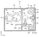
- the bonding apparatus 41 includes a processing container 70 that can seal the inside.
- the side surface of the wafer transfer area 60 side of the processing container 70, the wafer W U, W L, the transfer port 71 of the overlapped wafer W T is formed, close shutter 72 is provided in the transfer port 71.
- an air flow that is called a downward flow is generated in the vertical downward direction.
- the atmosphere inside the processing container 70 is exhausted from the exhaust port 73 formed in the bottom face of the conveyance area
- the inside of the processing container 70 is partitioned into a transport region T1 and a processing region T2 by an inner wall 74.
- the carry-in / out port 71 described above is formed on the side surface of the processing container 70 in the transfer region T1.
- a loading / unloading port 75 for the wafers W U and W L and the overlapped wafer W T is formed on the inner wall 74.
- a transition 80 for temporarily placing the wafers W U and W L and the superposed wafer W T is provided on the positive side in the X direction of the transfer region T1.
- the transition 80 is formed, for example, in two stages, and any two of the wafers W U , W L , and the superposed wafer W T can be placed at the same time.
- a wafer transfer body 82 that is movable on a transfer path 81 extending in the X direction is provided. As shown in FIGS. 4 and 5, the wafer transfer body is also movable in the vertical direction and the vertical axis, and the wafers W U and W L in the transfer area T1 or between the transfer area T1 and the processing area T2. , it can transfer the overlapping wafer W T.
- the transfer path 81 and the wafer transfer body 82 constitute a transfer mechanism.
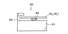
- a position adjustment mechanism 90 that adjusts the horizontal direction of the wafers W U and W L is provided on the negative side in the X direction of the transfer region T1.
- Position adjusting mechanism 90 includes a base 91 as shown in FIG. 6, a holding portion 92 for rotating the wafer W U, the W L adsorbed and held, detection for detecting a position of the notch portion of the wafer W U, W L Part 93. Then, the position adjusting mechanism 90, the wafer W U sucked and held by the holding portion 92, the detection unit 93 while rotating the W L by detecting the position of the notch portion of the wafer W U, W L, the notch Are adjusted to adjust the horizontal orientation of the wafers W U and W L.
- the processing region T2 the lower chuck 100 as a first holding member for holding by placing the lower wafer W L with the upper surface as shown in FIGS. 4 and 5, for attracting and holding the upper wafer W U with lower surface
- An upper chuck 101 as a second holding member is provided.
- the upper chuck 101 is provided above the lower chuck 100 and is configured so as to be opposed to the lower chuck 100. That is, the upper wafer W U held in the lower wafer W L and the upper chuck 101 held by the lower chuck 100 is adapted to be placed opposite.
- a suction pipe (not shown) communicating with a vacuum pump (not shown) is provided inside the lower chuck 100. By suction through the suction pipe, it attracts and holds the lower wafer W L on the upper surface of the lower chuck 100.
- a chuck driving unit 103 is provided via a shaft 102 as shown in FIG.
- the lower chuck 100 can be raised and lowered by the chuck driving unit 103.
- the lower chuck 100 may be movable in the horizontal direction by the chuck driving unit 103, and may be further rotatable about the vertical axis.
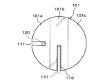
- the upper chuck 101 is formed with two notches 110 and 111 as shown in FIG.
- the 1st notch part 110 is formed so that it may not interfere with the holding arm 131 of the inversion mechanism 130 mentioned later.
- the 2nd notch part 111 is formed so that it may not interfere with the pushing member 120 mentioned later.
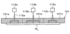
- the inside of the upper chuck 101 is partitioned into a plurality of, for example, three regions 101a, 101b, and 101c as shown in FIG.
- Each region 101a, 101b, the 101c, the suction pipe 112a for sucking and holding the upper wafer W U, 112b, 112c are provided independently.
- the suction pipes 112a, 112b, and 112c are connected to different vacuum pumps 113a, 113b, and 113c, respectively.
- a rail 114 extending along the Y direction is provided above the upper chuck 101 as shown in FIG.
- the upper chuck 101 is movable on the rail 114 by a chuck driving unit 115.
- the upper chuck 101 may be movable in the vertical direction by the chuck driving unit 115, and may be further rotatable around the vertical axis.
- the upper chuck 101, the rail 114, and the chuck driving unit 115 constitute a moving mechanism.
- a push member 120 is provided in the processing region T2.
- the pushing member 120 is configured to be movable up and down by a driving unit 121 such as a cylinder. Then, the pressing member 120, the wafer W U to be described later, at the time of bonding of W L, one end portion of the lower wafer W L, the one end portion of the upper wafer W U facing the one end of the lower wafer W L equivalent It can be pressed in contact.
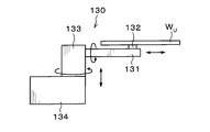
- the transfer region T1 is reversing mechanism 130 which moves between the transfer region T1 and the processing region T2, to and reverses the front and rear surfaces of the upper wafer W U is provided.
- Reversing mechanism 130 has a holding arm 131 which holds the upper wafer W U as shown in FIG. On the holding arm 131, the suction pads 132 held horizontally by suction on the wafer W U is provided.
- the holding arm 131 is supported by the first driving unit 133. By this first drive unit 133, the holding arm 131 is rotatable about a horizontal axis and can be expanded and contracted in the horizontal direction.
- a second drive unit 134 is provided below the first drive unit 133.
- the first drive unit 133 is rotatable about the vertical axis and can be moved up and down in the vertical direction.
- the second drive unit 134 is attached to a rail 135 extending in the Y direction shown in FIGS. 4 and 5.
- the rail 135 extends from the processing area T2 to the transport area T1.
- the reversing mechanism 130 can move between the position adjusting mechanism 90 and the upper chuck 101 along the rail 135 by the second driving unit 134.
- the configuration of the reversing mechanism 130 is not limited to the configuration of the above embodiment, it is sufficient to invert the front and rear surfaces of the upper wafer W U. Further, the reversing mechanism 130 may be provided in the processing region T2. Further, a reversing mechanism may be added to the wafer transport body 82, and another transport means may be provided at the position of the reversing mechanism 130.
- an upper imaging member for imaging the surface W U1 of the lower imaging member and the upper wafer W U is provided for imaging the surface W L1 of W L.
- a wide-angle CCD camera is used for the lower imaging member and the upper imaging member.
- the bonding device 41 when joining the wafer W U, W L in the bonding apparatus 41 configured as described above, the bonding device 41, the outside of the joint device 41, that air flow generated between the wafer transfer area 60, and The airflow generated in the joining device 41 will be described with reference to FIG.
- the arrow in FIG. 10 has shown the direction of the airflow.
- the pressure in the bonding apparatus 41 is positive with respect to the pressure in the wafer transfer region 60. Therefore, when the opening / closing shutter 71 is opened, an air flow from the bonding apparatus 41 toward the wafer transfer region 60 is generated.
- the atmosphere inside the processing container 70 is exhausted from the exhaust port 73 of the transfer region T1. Accordingly, an airflow is generated from the processing region T2 toward the transfer region T1 via the loading / unloading port 75.
- the above joining system 1 is provided with a control unit 200 as shown in FIG.
- the control unit 200 is a computer, for example, and has a program storage unit (not shown).
- the program storage unit stores a program for controlling processing of the wafers W U and W L and the overlapped wafer W T in the bonding system 1.
- the program storage unit also stores a program for controlling the operation of drive systems such as the above-described various processing apparatuses and transfer apparatuses to realize the below-described joining process in the joining system 1.
- the program is recorded on a computer-readable storage medium H such as a computer-readable hard disk (HD), a flexible disk (FD), a compact disk (CD), a magnetic optical desk (MO), or a memory card. May have been installed in the control unit 200 from the storage medium H.
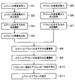
- FIG. 11 is a flowchart showing an example of main steps of the wafer bonding process.
- the cassette C U, the cassette C L accommodating the lower wafer W L of the plurality, and the empty cassette C T is a predetermined cassette mounting plate 11 of the carry-out station 2 accommodating the wafers W U on the plurality Placed on. Thereafter, the upper wafer W U in the cassette C U is taken out by the wafer transfer device 22 is conveyed to the transition unit 50 of the third processing block G3 in the processing station 3.
- the upper wafer W U is transported to the first processing block surface activation device G1 30 by the wafer transfer apparatus 61.
- the surface W U1 of the wafer W U is activated using radicals obtained by plasma-exciting the processing gas (step S ⁇ b> 1 in FIG. 11).
- the upper wafer W U is transferred to a surface hydrophilizing apparatus 40 of the second processing block G2 by the wafer transfer apparatus 61.
- the surface hydrophilizing apparatus 40 for example by supplying pure water onto the upper wafer W U, the surface W U1 and hydroxyl groups on the surface W U1 of the on wafer W U is attached is hydrophilized. Further, the surface W U1 of the upper wafer W U is cleaned by this pure water (step S2 in FIG. 11).
- the upper wafer W U is transferred to the bonding apparatus 41 of the second processing block G2 by the wafer transfer apparatus 61.
- Upper wafer W U which is carried into the joining device 41 is conveyed to the position adjusting mechanism 90 by the wafer carrier 82 via a transition 80.
- the position adjustment mechanism 90 the horizontal orientation of the upper wafer W U is adjusted (step S3 in FIG. 11).
- the upper wafer W U is transferred from the position adjusting mechanism 90 to the holding arm 131 of the reversing mechanism 130. Subsequently, in transfer region T1, by reversing the holding arm 131, the front and back surfaces of the upper wafer W U is inverted (step S4 in FIG. 11). That is, the surface W U1 of the upper wafer W U is directed downward. Thereafter, the reversing mechanism 130 is moved to the upper chuck 101, the upper wafer W U is transferred from the inverting mechanism 130 in the upper chuck 101. Upper wafer W U, the back surface W U2 on the upper chuck 101 is held by suction.
- the upper chuck 101 is moved by the chuck driving unit 115 to a position above the lower chuck 100 and facing the lower chuck 100.
- the upper wafer W U the process waits at the upper chuck 101 to the lower wafer W L is transported to the bonding apparatus 41 described later. Note that the reversal of the front and back surfaces of the upper wafer W U may be performed while the reversing mechanism 130 is moving.
- the processing of the lower wafer W L Following the on wafer W U is performed.
- the lower wafer W L in the cassette C L is taken out by the wafer transfer device 22 is conveyed to the transition unit 50 in the processing station 3.
- step S5 the surface W L1 of the lower wafer W L is activated (step S5 in FIG. 11). Note that activation of the surface W L1 of the lower wafer W L in step S5, the same as the process S1 described above.
- step S6 hydrophilic and cleaning of the surface W L1 of the lower wafer W L in step S6 is the same as step S2 of the above-described.
- the lower wafer W L is transported to the bonding apparatus 41 by the wafer transfer apparatus 61.
- Lower wafer W L which is transported to the bonding unit 41 is conveyed to the position adjusting mechanism 90 by the wafer carrier 82 via a transition 80.
- the position adjustment mechanism 90, the horizontal orientation of the lower wafer W L are adjusted (step S7 in FIG. 11).
- the lower wafer W L is transferred to the lower chuck 100 by the wafer transfer body 82 is attracted and held by the lower chuck 100.
- the surface W L1 of the lower wafer W L is to face upwards
- the back surface W L2 of the lower wafer W L is held by the lower chuck 100.
- the upper surface of the lower chuck 100 fits a groove in the shape of the wafer transfer body 82 is formed, and a wafer carrier 82 during the transfer of the lower wafer W L and the lower chuck 100 is interfering May be avoided.
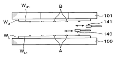
- the adjusted horizontal positions of the upper wafer W U held in the lower wafer W L and the upper chuck 101 held by the lower chuck 100 As shown in FIG. 12, a plurality of predetermined reference points A are formed on the surface W L1 of the lower wafer W L , and similarly, a plurality of predetermined reference points B are formed on the surface W U1 of the upper wafer W U. Is formed. Then, by moving the lower imaging member 140 in the horizontal direction, the surface W L1 of the lower wafer W L is imaged. Further, the upper imaging member 141 is moved in the horizontal direction, and the surface W U1 of the upper wafer W U is imaged.
- the position of the reference point A of the lower wafer W L of the lower imaging member 140 is displayed in the image captured, and the position of the reference point B of the wafer W U on the upper imaging member 141 are displayed on the image captured Consistently, the horizontal position of the upper wafer W U is regulated by the upper chuck 101. Horizontal position of the upper wafer W U and the lower wafer W L is adjusted in this way (step S8 in FIG. 11).
- the lower imaging member 140 and the upper imaging member 141 constitute another position adjustment mechanism.
- the lower chuck 100 when the lower chuck 100 is horizontally movable by the chuck drive unit 103 may adjust the horizontal position of the lower wafer W L by the lower chuck 100 and lower chuck 100 and upper chuck The relative horizontal position of the lower wafer W L and the upper wafer W U may be adjusted by both 101.
- the chuck drive unit 103 raises the lower chuck 100 as shown in FIG. 13, to place the lower wafer W L to a predetermined position.
- the distance D between the surface W U1 of the surface W L1 and the upper wafer W U of the lower wafer W L is a predetermined distance, for example 0.5 mm, placing the lower wafer W L.
- Vertical position of the upper wafer W U and the lower wafer W L is adjusted in this way (step S9 in FIG. 11).
- step S10 in FIG. 11 pressed by abutting the one end portion of the one end and the upper wafer W U of the lower wafer W L to lower the pressing member 120 as shown in FIG. 14 (step S10 in FIG. 11).
- all regions 101a of the upper chuck 101, 101b, in 101c, are evacuated upper wafer W U.
- step S1 and S5 Since the surface W U1 of the upper wafer W U and the surface W L1 of the lower wafer W L are activated in steps S1 and S5, respectively, first, van der Waals force is generated between the surfaces W U1 and W L1. The surfaces W U1 and W L1 are joined to each other. Thereafter, the surface W U1 of the upper wafer W U and the surface W L1 of the lower wafer W L are hydrophilized in steps S2 and S6, respectively, so that the hydrophilic group between the surfaces W U1 and W L1 is hydrogen-bonded. U1 and WL1 are firmly joined to each other. Thus the upper wafer W U and the lower wafer W L is bonded (step S11 in FIG. 11).
- the region 101a in the present embodiment, 101b have been stopped evacuation of the upper wafer W U in the order of 101c, how to stop evacuation is not limited thereto.
- the evacuation may be stopped simultaneously in the regions 101a and 101b, and then the evacuation may be stopped in the region 101c.
- the time interval for stopping the evacuation between the regions 101a, 101b, and 101c may be changed.
- the evacuation in the region 101b is stopped 1 second after the evacuation in the region 101a is stopped, and the evacuation in the region 101c is stopped 2 seconds after the evacuation in the region 101b is further stopped. May be.
- the upper wafer W U and the lower wafer W L overlapped wafer bonded W T is transferred to the transition unit 51 by the wafer transfer apparatus 61, then carry out by the wafer transfer apparatus 22 of the station 2 of a predetermined cassette mounting plate 11 It is conveyed to the cassette C T.
- a series of wafers W U, bonding process of W L is completed.
- the step S11 in the bonding apparatus 41 in a state where one end portion of the one end and the upper wafer W U of the lower wafer W L is pressed, the other from one end side of the upper wafer W U toward the end portion side, by sequentially contacting the on wafer W U to the lower wafer W L.
- the air can be a void between the lower wafer W L and the upper wafer W U is present, always outside the places air to the upper wafer W U is in contact with the lower wafer W L, i.e. It exists on the other end side, and the air can be released in one direction from between the wafers W U and W L.
- the lower wafer in a state in which the upper wafer W U is held in the upper chuck 101, since it is possible to contact the one end of the one end portion and the lower wafer W L of the upper wafer W U, the lower wafer The position of the upper wafer W U with respect to W L is not shifted, and the wafers W U and W L can be appropriately joined.
- the upper chuck 101 of the joining device 41 a plurality of regions 101a, 101b, is divided into 101c, the area 101a, 101b, since it is possible to set the vacuum of the upper wafer W U per 101c, in step S11, from one end side of the upper wafer W U toward the other end side, the on wafer W U can reliably turn contacts the lower wafer W L. Therefore, it is possible to escape the air between the wafer W U, W L, to reliably suppress generation of voids between the wafer W U, W L.
- the surfaces of the wafers W U and W L are activated in steps S1 and S4 in the surface activation device 30, and the surfaces W U1 and W of the wafers W U and W L in steps S2 and S5 in the surface hydrophilization device 40.
- L1 is hydrophilized and hydroxylated on the surfaces W U1 and W L1 .
- the surfaces W U1 and W L1 of the activated wafers W U and W L are bonded to each other by van der Waals force, and then the surfaces of the wafers W U and W L that have been hydrophilized.
- the hydroxyl groups of W U1 and W L1 can be hydrogen bonded to bond the wafers W U and W L firmly together.
- the wafer W U in step S3, S6 of the joining device 41 to adjust the respective horizontal orientation of W L, to adjust the position of the horizontal and vertical directions of the wafer W U, W L in step S8, S9 ing. Therefore, the wafers W U and W L can be appropriately bonded in the subsequent step S11.
- the pressure in the bonding apparatus 41 is a positive pressure relative to the pressure in the wafer transfer area 60, so that an air flow from the bonding apparatus 41 toward the wafer transfer area 60 is generated. That is, no atmosphere flows into the bonding apparatus 41 from the outside. Therefore, without particles or the like is introduced from the outside into the junction device 41, the wafer W U, the junction of the W L can be appropriately performed.
- the cooling mechanism 210 may be provided on the lower surface side of the lower chuck 100, and the cooling mechanism 211 may be provided on the upper surface side of the upper chuck 101.
- the cooling mechanisms 210 and 211 incorporate cooling members (not shown) such as cooling water and Peltier elements. Cooling temperature of the cooling mechanism 210 and 211 is controlled by a control unit 200 for example, lower wafer W L held by the lower chuck 100 is cooled to a predetermined temperature below room temperature (23 ° C.), also held by the upper chuck 101 the upper wafer W U were it is cooled to a predetermined temperature below room temperature (23 ° C.).
- the cooling mechanisms 210 and 211 are provided in both the lower chuck 100 and the upper chuck 101.
- the cooling mechanism 210 may be provided only in the lower chuck 100, or only in the upper chuck 101.
- a cooling mechanism 211 may be provided.
- in the third processing block G3 in the processing station 3 be provided with a cooling device for cooling the bonded overlapped wafer W T are laminated in the transition unit 50, 51 Good.
- the wafer W U, W L are joined.
- the wafers W U and W L are cooled to a room temperature or lower, bonding and hydrogen bonding by the van der Waals forces of the surfaces W U1 and W L1 of the wafers W U and W L are promoted. Therefore, the throughput of the wafer bonding process can be further improved.
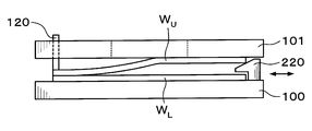
- a guide member 220 that is movable in the horizontal direction between the lower chuck 100 and the upper chuck 101 may be disposed as shown in FIG.
- the guide member 220 is disposed to face the pushing member 120.
- the guide member 220 supports the other end of the upper wafer W U held by the upper chuck 101, that is, the end facing the one end of the upper wafer W U pressed by the pushing member 120. Supporting surface of the upper wafer W U in the guide member 220 is inclined from the horizontal direction. Further, the guide member 220 is provided so as not to abut against the lower wafer W L held by the lower chuck 100.
- the guide member 220 toward the one end side of the upper wafer W U to the other end side, the upper wafer W U can reliably turn contacts the lower wafer W L. Therefore, it is possible to escape the air between the wafer W U, W L, to reliably suppress generation of voids between the wafer W U, W L.
- the present invention is not limited to such examples. It is obvious for those skilled in the art that various modifications or modifications can be conceived within the scope of the idea described in the claims, and these naturally belong to the technical scope of the present invention. It is understood.
- the present invention is not limited to this example and can take various forms.
- the present invention can also be applied to a case where the substrate is another substrate such as an FPD (flat panel display) other than a wafer or a mask reticle for a photomask.
- FPD flat panel display
- the present invention is useful when bonding substrates such as semiconductor wafers.
Landscapes
- Container, Conveyance, Adherence, Positioning, Of Wafer (AREA)
- Wire Bonding (AREA)
- Pressure Welding/Diffusion-Bonding (AREA)
Abstract
Description
41 接合装置
70 処理容器
73 排気口
80 トランジション
81 搬送路
82 ウェハ搬送体
90 位置調節機構
100 下部チャック
101 上部チャック
101a、101b、101c 領域
112a、112b、112c 吸引管
113a、113b、113c 真空ポンプ
114 レール
115 チャック駆動部
120 押動機構
130 反転機構
140 下部撮像部材
141 上部撮像部材
200 制御部
210、211 冷却機構
220 ガイド部材
A、B 基準点
WU 上ウェハ
WU1 表面
WL 下ウェハ
WL1 表面
WT 重合ウェハ
Claims (8)
- 基板同士を接合する接合装置であって、
上面に第1の基板を載置して保持する第1の保持部材と、
前記第1の保持部材の上方に当該第1の保持部材と対向して設けられ、下面に第2の基板を保持する第2の保持部材と、
第1の基板と第2の基板の接合時に、第1の基板の一端部と、当該第1の基板の一端部に対向する第2の基板の一端部とを当接させて押圧する押動部材と、
第2の基板の表裏面を反転させる反転機構と、
前記接合装置内で第1の基板、第2の基板又は重合基板を搬送する搬送機構と、を有する。 - 請求項1に記載の接合装置であって、
第2の保持部材は、第2の基板を真空引きして吸着保持し、
当該第2の保持部材は、複数の領域に区画され、当該領域毎に第2の基板の真空引きを設定可能である。 - 請求項1に記載の接合装置であって、
前記接合装置内の圧力は、外部の圧力に対して陽圧である。 - 請求項1に記載の接合装置であって、
少なくとも前記第1の保持部材又は前記第2の保持部材は、少なくとも第1の基板又は第2の基板を冷却する冷却機構を有する。 - 請求項1に記載の接合装置であって、
第1の基板又は第2の基板の水平方向の向きを調節する位置調節機構を有し、
前記反転機構は、前記位置調節機構と前記第2の保持部材との間を移動可能である。 - 請求項1に記載の接合装置であって、
第1の基板、第2の基板又は重合基板を外部との間で搬入出するために、当該第1の基板、第2の基板又は重合基板を一時的に載置するトランジションを有する。 - 請求項1に記載の接合装置であって、
前記第1の保持部材及び前記第2の保持部材の間であって、前記押動部材に対向して配置されるガイド部材を有し、
前記ガイド部材は、前記第2の保持部材に保持された第2の基板の他端部を支持し、且つ水平方向に移動自在に構成されている。 - 請求項1に記載の接合装置であって、
前記第1の保持部材又は第2の保持部材を相対的に水平方向に移動させる移動機構と、
前記第1の保持部材に保持された第1の基板と、前記第2の保持部材に保持された第2の基板との水平方向の位置合わせを行うために前記移動機構を制御する他の位置調節機構を有し、
前記他の位置調節機構は、第1の基板の表面を撮像する第1の撮像部材と、第2の基板の表面を撮像する第2の撮像部材とを有し、
前記移動機構は、前記第1の撮像部材によって撮像された画像における第1の基板の基準点と、前記第2の撮像部材によって撮像された画像における第2の基板の基準点と、が合致するように前記第1の保持部材と前記第2の保持部材の相対的な水平方向の位置を調節する。
Priority Applications (2)
| Application Number | Priority Date | Filing Date | Title |
|---|---|---|---|
| US13/574,798 US8819923B2 (en) | 2010-02-26 | 2011-02-21 | Joint apparatus |
| KR1020127022200A KR101384461B1 (ko) | 2010-02-26 | 2011-02-21 | 접합 장치 |
Applications Claiming Priority (2)
| Application Number | Priority Date | Filing Date | Title |
|---|---|---|---|
| JP2010043380A JP5355451B2 (ja) | 2010-02-26 | 2010-02-26 | 接合装置 |
| JP2010-043380 | 2010-02-26 |
Publications (1)
| Publication Number | Publication Date |
|---|---|
| WO2011105326A1 true WO2011105326A1 (ja) | 2011-09-01 |
Family
ID=44506734
Family Applications (1)
| Application Number | Title | Priority Date | Filing Date |
|---|---|---|---|
| PCT/JP2011/053674 Ceased WO2011105326A1 (ja) | 2010-02-26 | 2011-02-21 | 接合装置 |
Country Status (5)
| Country | Link |
|---|---|
| US (1) | US8819923B2 (ja) |
| JP (1) | JP5355451B2 (ja) |
| KR (1) | KR101384461B1 (ja) |
| TW (1) | TWI474420B (ja) |
| WO (1) | WO2011105326A1 (ja) |
Cited By (1)
| Publication number | Priority date | Publication date | Assignee | Title |
|---|---|---|---|---|
| US20130062013A1 (en) * | 2011-09-13 | 2013-03-14 | Tokyo Electron Limited | Joint apparatus, joint system, and joint method |
Families Citing this family (11)
| Publication number | Priority date | Publication date | Assignee | Title |
|---|---|---|---|---|
| US7829152B2 (en) * | 2006-10-05 | 2010-11-09 | Lam Research Corporation | Electroless plating method and apparatus |
| JP2014072321A (ja) * | 2012-09-28 | 2014-04-21 | Hitachi High-Technologies Corp | 板状体保持機構、基板貼り合わせ装置及び基板貼り合わせ方法 |
| JP2014229677A (ja) | 2013-05-21 | 2014-12-08 | 東京エレクトロン株式会社 | 接合装置、接合システム、接合方法、プログラム及びコンピュータ記憶媒体 |
| JP2015015269A (ja) * | 2013-07-03 | 2015-01-22 | 東京エレクトロン株式会社 | 接合装置、接合システム、接合方法、プログラム及びコンピュータ記憶媒体 |
| JP6047452B2 (ja) * | 2013-07-10 | 2016-12-21 | 東京エレクトロン株式会社 | 接合装置、接合システム、接合方法、プログラム及びコンピュータ記憶媒体 |
| JP6280332B2 (ja) * | 2013-09-09 | 2018-02-14 | 三星ダイヤモンド工業株式会社 | 基板反転搬送装置 |
| JP6128337B2 (ja) * | 2014-10-23 | 2017-05-17 | パナソニックIpマネジメント株式会社 | 半導体装置の製造方法及び製造装置 |
| JP6731805B2 (ja) * | 2016-07-12 | 2020-07-29 | 東京エレクトロン株式会社 | 接合システム |
| TWI608573B (zh) * | 2016-10-27 | 2017-12-11 | 兆遠科技股份有限公司 | Composite substrate bonding method |
| KR102459089B1 (ko) * | 2017-12-21 | 2022-10-27 | 삼성전자주식회사 | 반도체 패키징 장비 및 이를 이용한 반도체 소자의 제조방법 |
| KR102679253B1 (ko) * | 2021-12-30 | 2024-06-26 | 세메스 주식회사 | 본딩 장치 및 본딩 방법 |
Citations (9)
| Publication number | Priority date | Publication date | Assignee | Title |
|---|---|---|---|---|
| JPH076937A (ja) * | 1993-06-16 | 1995-01-10 | Canon Inc | 半導体基板貼り合わせ装置 |
| JPH10256107A (ja) * | 1997-03-13 | 1998-09-25 | Canon Inc | 基板処理装置及びその方法並びに基板の製造方法 |
| JP2004207436A (ja) * | 2002-12-25 | 2004-07-22 | Ayumi Kogyo Kk | ウエハのプリアライメント方法とその装置ならびにウエハの貼り合わせ方法とその装置 |
| JP2007036130A (ja) * | 2005-07-29 | 2007-02-08 | Canon Inc | 熱膨張係数の差を利用した基板接合方法及び装置 |
| JP2007201196A (ja) * | 2006-01-26 | 2007-08-09 | Matsushita Electric Works Ltd | ウェハ接合装置およびウェハ接合方法 |
| JP2009049081A (ja) * | 2007-08-15 | 2009-03-05 | Nikon Corp | 接合装置 |
| JP2009200156A (ja) * | 2008-02-20 | 2009-09-03 | Citizen Holdings Co Ltd | 接合装置 |
| WO2009139190A1 (ja) * | 2008-05-15 | 2009-11-19 | 株式会社ニコン | 位置検出装置、基板重ね合わせ装置 |
| JP2010034445A (ja) * | 2008-07-31 | 2010-02-12 | Sumco Corp | ウェーハ自動貼合せ装置およびウェーハ自動貼合せ方法 |
Family Cites Families (3)
| Publication number | Priority date | Publication date | Assignee | Title |
|---|---|---|---|---|
| US6790300B2 (en) * | 2000-09-14 | 2004-09-14 | Hitachi Electronics Engineering Co., Ltd. | Method and apparatus for bonding substrate plates together through gap-forming sealer material |
| JP2003243479A (ja) * | 2002-02-19 | 2003-08-29 | Tokyo Electron Ltd | 搬送手段の停止位置調整機構 |
| EP2216802A1 (de) * | 2005-10-13 | 2010-08-11 | Erich Dipl.-Ing. Thallner | Vorrichtung zum Bonden von Wafern |
-
2010
- 2010-02-26 JP JP2010043380A patent/JP5355451B2/ja active Active
-
2011
- 2011-02-21 WO PCT/JP2011/053674 patent/WO2011105326A1/ja not_active Ceased
- 2011-02-21 US US13/574,798 patent/US8819923B2/en active Active
- 2011-02-21 KR KR1020127022200A patent/KR101384461B1/ko active Active
- 2011-02-24 TW TW100106282A patent/TWI474420B/zh active
Patent Citations (9)
| Publication number | Priority date | Publication date | Assignee | Title |
|---|---|---|---|---|
| JPH076937A (ja) * | 1993-06-16 | 1995-01-10 | Canon Inc | 半導体基板貼り合わせ装置 |
| JPH10256107A (ja) * | 1997-03-13 | 1998-09-25 | Canon Inc | 基板処理装置及びその方法並びに基板の製造方法 |
| JP2004207436A (ja) * | 2002-12-25 | 2004-07-22 | Ayumi Kogyo Kk | ウエハのプリアライメント方法とその装置ならびにウエハの貼り合わせ方法とその装置 |
| JP2007036130A (ja) * | 2005-07-29 | 2007-02-08 | Canon Inc | 熱膨張係数の差を利用した基板接合方法及び装置 |
| JP2007201196A (ja) * | 2006-01-26 | 2007-08-09 | Matsushita Electric Works Ltd | ウェハ接合装置およびウェハ接合方法 |
| JP2009049081A (ja) * | 2007-08-15 | 2009-03-05 | Nikon Corp | 接合装置 |
| JP2009200156A (ja) * | 2008-02-20 | 2009-09-03 | Citizen Holdings Co Ltd | 接合装置 |
| WO2009139190A1 (ja) * | 2008-05-15 | 2009-11-19 | 株式会社ニコン | 位置検出装置、基板重ね合わせ装置 |
| JP2010034445A (ja) * | 2008-07-31 | 2010-02-12 | Sumco Corp | ウェーハ自動貼合せ装置およびウェーハ自動貼合せ方法 |
Cited By (3)
| Publication number | Priority date | Publication date | Assignee | Title |
|---|---|---|---|---|
| US20130062013A1 (en) * | 2011-09-13 | 2013-03-14 | Tokyo Electron Limited | Joint apparatus, joint system, and joint method |
| TWI567849B (zh) * | 2011-09-13 | 2017-01-21 | 東京威力科創股份有限公司 | 接合裝置、接合系統、接合方法及電腦記憶媒體 |
| KR101849788B1 (ko) * | 2011-09-13 | 2018-04-17 | 도쿄엘렉트론가부시키가이샤 | 접합 장치, 접합 시스템, 접합 방법 및 컴퓨터 기억 매체 |
Also Published As
| Publication number | Publication date |
|---|---|
| US8819923B2 (en) | 2014-09-02 |
| TWI474420B (zh) | 2015-02-21 |
| KR20120117904A (ko) | 2012-10-24 |
| TW201207974A (en) | 2012-02-16 |
| US20120291267A1 (en) | 2012-11-22 |
| JP2011181633A (ja) | 2011-09-15 |
| KR101384461B1 (ko) | 2014-04-10 |
| JP5355451B2 (ja) | 2013-11-27 |
Similar Documents
| Publication | Publication Date | Title |
|---|---|---|
| JP5355451B2 (ja) | 接合装置 | |
| TWI594308B (zh) | 接合裝置、接合系統、接合方法及電腦記憶媒體 | |
| JP5421825B2 (ja) | 接合システム、接合方法、プログラム及びコンピュータ記憶媒体 | |
| TWI595593B (zh) | 接合裝置及接合系統 | |
| TWI600055B (zh) | 接合方法、電腦記錄媒體、接合裝置及接合系統 | |
| TWI612595B (zh) | 接合裝置、接合系統、接合方法及電腦記憶媒體 | |
| KR102073996B1 (ko) | 접합 장치, 접합 시스템, 접합 방법 및 컴퓨터 기억 매체 | |
| JP2015018920A (ja) | 接合装置、接合システム、接合方法、プログラム及びコンピュータ記憶媒体 | |
| JP2015018919A (ja) | 接合装置、接合システム、接合方法、プログラム及びコンピュータ記憶媒体 | |
| JP2012186245A (ja) | 接合装置、接合システム、接合方法、プログラム及びコンピュータ記憶媒体 | |
| JP2015119088A (ja) | 接合方法、プログラム、コンピュータ記憶媒体、接合装置及び接合システム | |
| JP2013214676A (ja) | 剥離システム、剥離方法、プログラム及びコンピュータ記憶媒体 | |
| JP2017034107A (ja) | 接合装置、接合システム、接合方法、プログラム及びコンピュータ記憶媒体 | |
| JP2015015269A (ja) | 接合装置、接合システム、接合方法、プログラム及びコンピュータ記憶媒体 | |
| JP6120749B2 (ja) | 接合方法、プログラム、コンピュータ記憶媒体、接合装置及び接合システム | |
| WO2011105325A1 (ja) | 接合方法、プログラム及びコンピュータ記憶媒体 | |
| JP2014229787A (ja) | 接合装置、接合システム、接合方法、プログラム及びコンピュータ記憶媒体 | |
| JP2015095649A (ja) | 接合装置及び接合システム | |
| JP6382765B2 (ja) | 接合装置及び接合システム | |
| JP2013232685A (ja) | 接合装置 | |
| JP6382764B2 (ja) | 接合装置及び接合システム |
Legal Events
| Date | Code | Title | Description |
|---|---|---|---|
| 121 | Ep: the epo has been informed by wipo that ep was designated in this application |
Ref document number: 11747287 Country of ref document: EP Kind code of ref document: A1 |
|
| WWE | Wipo information: entry into national phase |
Ref document number: 13574798 Country of ref document: US |
|
| ENP | Entry into the national phase |
Ref document number: 20127022200 Country of ref document: KR Kind code of ref document: A |
|
| NENP | Non-entry into the national phase |
Ref country code: DE |
|
| 122 | Ep: pct application non-entry in european phase |
Ref document number: 11747287 Country of ref document: EP Kind code of ref document: A1 |