WO2011105163A1 - プラズマ成膜装置及び方法 - Google Patents
プラズマ成膜装置及び方法 Download PDFInfo
- Publication number
- WO2011105163A1 WO2011105163A1 PCT/JP2011/051689 JP2011051689W WO2011105163A1 WO 2011105163 A1 WO2011105163 A1 WO 2011105163A1 JP 2011051689 W JP2011051689 W JP 2011051689W WO 2011105163 A1 WO2011105163 A1 WO 2011105163A1
- Authority
- WO
- WIPO (PCT)
- Prior art keywords
- substrate
- film
- plasma
- borazine
- electrode
- Prior art date
- Legal status (The legal status is an assumption and is not a legal conclusion. Google has not performed a legal analysis and makes no representation as to the accuracy of the status listed.)
- Ceased
Links
Images


Classifications
-
- C—CHEMISTRY; METALLURGY
- C23—COATING METALLIC MATERIAL; COATING MATERIAL WITH METALLIC MATERIAL; CHEMICAL SURFACE TREATMENT; DIFFUSION TREATMENT OF METALLIC MATERIAL; COATING BY VACUUM EVAPORATION, BY SPUTTERING, BY ION IMPLANTATION OR BY CHEMICAL VAPOUR DEPOSITION, IN GENERAL; INHIBITING CORROSION OF METALLIC MATERIAL OR INCRUSTATION IN GENERAL
- C23C—COATING METALLIC MATERIAL; COATING MATERIAL WITH METALLIC MATERIAL; SURFACE TREATMENT OF METALLIC MATERIAL BY DIFFUSION INTO THE SURFACE, BY CHEMICAL CONVERSION OR SUBSTITUTION; COATING BY VACUUM EVAPORATION, BY SPUTTERING, BY ION IMPLANTATION OR BY CHEMICAL VAPOUR DEPOSITION, IN GENERAL
- C23C16/00—Chemical coating by decomposition of gaseous compounds, without leaving reaction products of surface material in the coating, i.e. chemical vapour deposition [CVD] processes
- C23C16/44—Chemical coating by decomposition of gaseous compounds, without leaving reaction products of surface material in the coating, i.e. chemical vapour deposition [CVD] processes characterised by the method of coating
- C23C16/50—Chemical coating by decomposition of gaseous compounds, without leaving reaction products of surface material in the coating, i.e. chemical vapour deposition [CVD] processes characterised by the method of coating using electric discharges
- C23C16/505—Chemical coating by decomposition of gaseous compounds, without leaving reaction products of surface material in the coating, i.e. chemical vapour deposition [CVD] processes characterised by the method of coating using electric discharges using radio frequency discharges
- C23C16/509—Chemical coating by decomposition of gaseous compounds, without leaving reaction products of surface material in the coating, i.e. chemical vapour deposition [CVD] processes characterised by the method of coating using electric discharges using radio frequency discharges using internal electrodes
-
- H—ELECTRICITY
- H01—ELECTRIC ELEMENTS
- H01J—ELECTRIC DISCHARGE TUBES OR DISCHARGE LAMPS
- H01J37/00—Discharge tubes with provision for introducing objects or material to be exposed to the discharge, e.g. for the purpose of examination or processing thereof
- H01J37/32—Gas-filled discharge tubes
- H01J37/32009—Arrangements for generation of plasma specially adapted for examination or treatment of objects, e.g. plasma sources
- H01J37/32082—Radio frequency generated discharge
- H01J37/321—Radio frequency generated discharge the radio frequency energy being inductively coupled to the plasma
-
- H—ELECTRICITY
- H01—ELECTRIC ELEMENTS
- H01J—ELECTRIC DISCHARGE TUBES OR DISCHARGE LAMPS
- H01J37/00—Discharge tubes with provision for introducing objects or material to be exposed to the discharge, e.g. for the purpose of examination or processing thereof
- H01J37/32—Gas-filled discharge tubes
- H01J37/32009—Arrangements for generation of plasma specially adapted for examination or treatment of objects, e.g. plasma sources
- H01J37/32082—Radio frequency generated discharge
- H01J37/32137—Radio frequency generated discharge controlling of the discharge by modulation of energy
- H01J37/32155—Frequency modulation
- H01J37/32165—Plural frequencies
-
- H—ELECTRICITY
- H01—ELECTRIC ELEMENTS
- H01J—ELECTRIC DISCHARGE TUBES OR DISCHARGE LAMPS
- H01J37/00—Discharge tubes with provision for introducing objects or material to be exposed to the discharge, e.g. for the purpose of examination or processing thereof
- H01J37/32—Gas-filled discharge tubes
- H01J37/32431—Constructional details of the reactor
- H01J37/32532—Electrodes
- H01J37/32541—Shape
Definitions
- the present invention relates to a plasma film forming apparatus and method for forming a film on a substrate with a source gas in a plasma state.
- a plasma film forming apparatus for example, a plasma CVD (Chemical Vapor Deposition) apparatus forms a film on a substrate by bringing a raw material gas into a plasma state and causing the raw material gases in a plasma state to react with each other.
- a bias is often applied to the substrate for the purpose of improving the quality of the formed film.
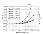
- FIG. 5 shows the results of measuring the radial thickness (X-axis position) of a borazine film formed by a conventional plasma CVD apparatus while changing the bias (LF) applied voltage.
- LF bias
- LF In the case of 50 W, 100 W, and 180 W, that is, when a bias is applied, the thickness of the substrate outer peripheral portion (see region A in FIG. 5) is higher than the central portion of the substrate, and desired film thickness uniformity can be obtained. I could not.
- the present invention has been made in view of the above problems, and an object thereof is to provide a plasma film forming apparatus and method capable of improving the uniformity of film thickness.
- a plasma film forming apparatus for solving the above-mentioned problems is as follows.
- a plasma film forming apparatus for applying a bias to the substrate when forming a film on the substrate by causing the source gas to be in a plasma state and reacting the source gases in a plasma state to each other,
- the size of the electrode for applying a bias to the substrate is larger than that of the substrate.
- a plasma film forming apparatus for solving the above-mentioned problems is as follows.
- R1 the radius of the substrate
- R2 the size of the electrode
- a plasma film forming method for solving the above problem is as follows: In the plasma film forming method of applying a bias to the substrate when forming a film on the substrate by causing the source gas to be in a plasma state and reacting the source gases in the plasma state to each other, A bias is applied to the substrate using an electrode larger than the size of the substrate.
- the size of the electrode for applying a bias to the substrate is made larger than the size of the substrate, it is possible to suppress an increase in the thickness of the outer peripheral portion of the substrate and improve the uniformity of the thickness. .
- FIG. 7 It is a see-through
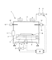
- FIG. 1 is a perspective side view showing an example of an embodiment of a plasma processing apparatus according to the present invention
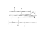
- FIG. 2 is a schematic configuration diagram showing a bias application electrode in the plasma processing apparatus shown in FIG.
- an ICP (Inductively-Coupled-Plasma) type plasma CVD apparatus 1 is shown as an example, but any apparatus having a plasma generation mechanism may be used.
- the plasma CVD apparatus 1 of the present embodiment is configured such that the inside of a cylindrical vacuum chamber 2 is configured as a film forming chamber, and a ceramic disk-shaped ceiling plate 3 is formed in the upper opening of the vacuum chamber 2. However, it is arrange
- a high-frequency antenna 4 made of, for example, a plurality of circular rings is disposed on the top (directly above) the ceiling plate 3, and a high-frequency power source 6 is connected to the high-frequency antenna 4 via a matching unit 5.
- the high-frequency power source 6 can feed a high oscillation frequency (for example, 13.56 MHz) to the high-frequency antenna 4 than the low-frequency power source 13 described later, and the electromagnetic waves that generate plasma in the vacuum chamber 2 are transmitted to the ceiling plate 3. Can enter through the light.
- This is a configuration of a so-called ICP type plasma generation mechanism. With an ICP type plasma generation mechanism, plasma with high electron density can be formed.
- a support base 7 and an electrostatic chuck 8 attached to the support base 7 are provided at the lower part of the vacuum chamber 2, and the upper surface of the electrostatic chuck 8 is made of a semiconductor material such as Si (silicon).
- a disk-shaped substrate W is electrostatically held by suction.
- the electrostatic chuck 8 is formed in a disk shape using a ceramic material such as aluminum nitride (AlN).
- the position of the support table 7 can be moved up and down by an elevating device 9, and the distance between the plasma generated in the vacuum chamber 2 and the substrate W during film formation can be adjusted. ing.
- the electrostatic chuck 8 is provided with a disk-shaped electrode 11, and a low frequency power source 13 is connected to the electrode 11 via a matching unit 12.
- the low frequency power supply 13 can apply a bias to the substrate W by applying an oscillation frequency (for example, 4 MHz) lower than that of the high frequency power supply 6 to the electrode 11.
- an oscillation frequency for example, 4 MHz
- the electrode 11 of the present embodiment is formed in a disk shape, for example, when the substrate W has an orientation flat, it may be formed to be similar to the shape.
- the support 7 is provided with a temperature control device such as a heater and a refrigerant flow path for controlling the temperature of the substrate W.
- the temperature control device (not shown) allows the substrate W to have a desired temperature (for example, 150). Can be set to ⁇ 700 ° C.
- the substrate W is transported onto the electrostatic chuck 8 by opening the gate door 17 provided on the side wall of the vacuum chamber 2. After placing the substrate W on the electrostatic chuck 8, the gate door 17 is closed. A process to be described later is performed inside the vacuum chamber 2.
- a plurality of gas nozzles 14 are provided on the side wall portion of the vacuum chamber 2 at a position lower than the ceiling plate 3 and higher than the support base 7, and are controlled from the gas nozzle 14 by controlling the gas control device 15.
- a gas having a desired flow rate can be supplied inside.
- the vacuum chamber 2 is provided with a pressure control device (vacuum pump, pressure control valve, vacuum gauge, etc .; not shown), and the inside of the vacuum chamber 2 is exhausted from the bottom side using the vacuum pump, The inside of the vacuum chamber 2 is adjusted to a desired pressure using a vacuum gauge and a pressure control valve.
- a pressure control device vacuum pump, pressure control valve, vacuum gauge, etc .; not shown
- the high-frequency power supply 6, the lifting device 9, the low-frequency power supply 13, the gas control device 15, the temperature control device, the pressure control device, and the like are integrally controlled by the main control device 16, and a desired process set in advance. It is controlled according to the process and process conditions.
- FIG. 6 shows a configuration of a conventional bias application electrode.
- the size of the bias application electrode 22 provided on the electrostatic chuck 21 is slightly smaller than the substrate W, as shown in FIG.
- R1 the radius of the substrate W
- R2 R1 ⁇ 1.0 mm is established so that R1> R2.
- the size of the bias application electrode 11 is made larger than that of the substrate W as shown in FIG.
- the radius of the substrate W is R1 and the radius of the electrode 11 is R2, the relation of R1 ⁇ R2 is established.
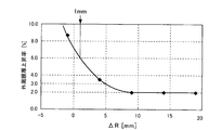
- FIG. 4 shows the film at the outer periphery of the substrate based on the result of FIG. The relationship between the rate of increase in thickness and ⁇ R is graphed. 3 and 4 also show the results of film formation using the conventional electrode 22 for comparison.
- the film thickness of the formed borazine film increases considerably as the outer edge of the substrate W is approached. It is assumed that this is because when the bias is applied to the substrate W, the electric field strength at the outer peripheral portion of the substrate W is increased, and as a result, the film forming rate at the outer peripheral portion of the substrate is increased.
- the tendency is considerably improved although the film thickness of the formed borazine film increases as it approaches the outer edge of the substrate W.
- the uniformity of the formed thin film is within 6% of the maximum value to the minimum value in the substrate surface.
- ⁇ R ⁇ 1 mm a desired value can be obtained.
- Uniformity can be obtained.
- at least ⁇ R ⁇ 5 mm may be set.
- ⁇ R ⁇ 9 mm the rate of increase in the outer peripheral film thickness is the lowest. In this case, the uniformity can be improved most.
- the diameter of the substrate W is 300 mm
- an electrostatic chuck having a size corresponding to the diameter is used. Since they are exchanged, the relation of R1> R2 is established, and the film thickness of the outer peripheral portion of the substrate tends to increase. Therefore, even when the diameter of the substrate W is smaller than 300 mm, the in-plane uniformity can be improved by satisfying the relationship of R1 ⁇ R2.
- the uniformity of the thickness of the thin film formed on the substrate can be improved. Further, suppressing the increase in the film thickness at the outer peripheral portion of the substrate alleviates the film stress at this portion, and as a result, the thin film is prevented from peeling off and the generation of particles is also suppressed.
- the film forming process of the borazine film will be described with reference to the plasma CVD apparatus 1 shown in FIG.
- the present invention is not limited to a borazine film but can be applied to other insulating films such as a silicon nitride film.
- an alkyl borazine compound represented by the following chemical formula 1 and a carrier gas are used as the source gas to be supplied.
- the side chain groups R1 to R6 in the chemical formula 1 are hydrogen atoms or alkyl groups having 5 or less carbon atoms, and may be the same or different. However, the case where all of R1 to R6 are hydrogen atoms is excluded. Among these, alkylborazine compounds in which at least one of R1, R3, and R5 is a hydrogen atom are preferable.
- the above-mentioned alkyl borazine compound is vaporized and then supplied to the vacuum chamber 2 using an inert gas as a carrier gas.
- a carrier gas a rare gas such as helium or argon or nitrogen is generally used.
- a mixed gas thereof or a mixed gas to which hydrogen, oxygen, ammonia, methane, or the like is added as necessary.
- the alkyl borazine compound is preferably a liquid at normal temperature and pressure, but may be a solid as long as it can be vaporized (sublimated) by heating or the like.
- a borazine film is formed by performing the following procedure using the above-described source gas.
- Step 1 The substrate W is transferred from the gate door 17 into the vacuum chamber 2 by using a transfer device (not shown), and is placed on the electrostatic chuck 8 and held by suction.
- the support base 7 and the electrostatic chuck 8 are heated to any temperature between 150 ° C. and 700 ° C., which is a temperature range in which the alkylborazine compound does not liquefy and the borazine skeleton molecules do not begin to condense with each other.
- the temperature of the substrate W is controlled so that the temperature of the substrate W can be processed at a desired set temperature. Further, the height position of the substrate W is moved by the lifting device 9 to any position within the range of 5 cm to 30 cm from the ceiling plate 3.
- a substrate W is disposed in the diffusion region. Therefore, during film formation, the alkyl group dissociated from the alkylborazine compound by plasma can be neutralized before being transported to the surface of the substrate W.
- the neutralized alkyl group has a low probability of recombination with the borazine skeleton molecule and is exhausted as it is.
- borazine skeleton molecules undergo gas phase polymerization, the incorporation of alkyl groups into the borazine film is reduced, and the amount of carbon in the thin film can be reduced.
- Molecules can be made high molecular weight to make a film with good characteristics.
- Step 2 The gas control device 15 is used to supply a carrier gas (for example, He gas) from the gas nozzle 14 into the vacuum chamber 2, and the degree of vacuum in the vacuum chamber 2 is controlled to about 10 to 50 mTorr by the vacuum control device.
- a carrier gas for example, He gas
- An RF power having a frequency of 13.56 MHz is supplied from the high frequency power source 6 to the high frequency antenna 4 through the vessel 5, electromagnetic waves are incident on the vacuum chamber 2, the supplied gas is ionized, and plasma is generated in the vacuum chamber 2. Is generated.
- the RF power supplied by the high-frequency power source 6 is within a power range in which the plasma is stably ignited until the series of processes is completed, and the side chain group of the borazine skeleton molecule can be dissociated without breaking the borazine skeleton structure. It is controlled by one of power of a 800W / m 2 ⁇ 53000W / m 2.
- the flow rate of the carrier gas supplied from the gas nozzle 14 is controlled to an appropriate flow rate until the series of processes is completed, but is preferably about 200 sccm to 1000 sccm.
- Step 3 After the stabilization of the plasma, an LF power having a frequency of 4 MHz is supplied from the low frequency power supply 13 to the electrode 11 through the matching unit 12 and the alkylborazine compound shown in the chemical formula 1 vaporized from the gas nozzle 14 in the vacuum chamber 2 is supplied.
- the pressure is gradually increased to a predetermined amount, and the degree of vacuum in the vacuum chamber 2 is controlled to about 10 to 50 mTorr.
- the LF power (bias power) supplied by the low-frequency power source 13 is controlled with a power of 14500 W / m 2 or less in the film forming process.
- gas phase polymerization between borazine skeleton-based molecules is promoted, so that not only the mechanical strength is improved but also water resistance, heat resistance, and chemical resistance are improved.
- At least one selected from the group consisting of ammonia and an amine compound containing an alkyl group having 1 to 3 carbon atoms may be supplied.
- the alkyl group dissociated from the alkyl borazine compound is desirably not taken into the borazine film to be formed, but at least one selected from the group consisting of ammonia and an amine compound containing an alkyl group having 1 to 3 carbon atoms.
- ethylamine C 2 H 5 NH 2
- an alkylamine which is a neutral molecule is obtained. Is unlikely to recombine with a borazine skeleton molecule, so it will be exhausted as it is.
- the film forming reaction in the film forming process is performed under the above process conditions. Specifically, the borazine skeleton molecule (borazine ring) and the side chain group in the alkyl borazine compound are dissociated by plasma, and the borazine skeleton molecules in the plasma state are vapor-phase polymerized to form a substrate W. A desired borazine film is formed by adsorbing to the surface.
- Step 4 When the film forming process is performed for a predetermined time and a borazine film having a desired film thickness is formed on the substrate W, the film forming process ends, and subsequently, a reaction promoting process is performed.
- the LF power from the low-frequency power source 13 that supplies power to the electrode 11 is made larger than the LF power in the film forming process, and the alkylborazine compound, ammonia, and carbon number 1 supplied from the gas nozzle 14 into the vacuum chamber 2.
- the amine compound containing ⁇ 3 alkyl groups is gradually reduced to only a rare gas (He, Ar, etc.) that does not react with the borazine film itself, or an inert gas such as N 2.
- the degree is controlled to about 10 to 50 mTorr.
- [LF power ⁇ application time] by the low-frequency power source 13 is controlled by electric power at which the LF power is not less than 254500 W / m 2 ⁇ sec and the LF power is not more than 127400 W / m 2 .
- This is a condition for accelerating the crosslinking reaction between borazine skeleton molecules but not causing damage to the thin film.
- the above process conditions promote the reaction in the reaction promoting step, that is, the crosslinking reaction between borazine skeleton-based molecules.
- the reactive group remaining in the borazine film formed in the film forming step is condensed to promote the crosslinking reaction and remove the BH bond. Accordingly, the promotion of the cross-linking reaction further promotes the reduction of the dielectric constant, and the removal of the B—H bond, which is the active site of the reaction with moisture, suppresses the change with time and improves the stability. Further, by promoting the crosslinking reaction, higher mechanical strength is achieved (mechanical strength Young's modulus of 10 GPa or more). As a result, chemical resistance is improved, workability is improved, and CMP (Chemical-Mechanical-Polish) resistance is improved. It will be. In addition, heat resistance can also be achieved because an inorganic polymer material superior in heat resistance compared to an organic polymer material is used.
- a borazine film having a small change with time in these characteristics is also realized. be able to.
- its specific characteristics include low dielectric constant (relative dielectric constant of 3.5 or less), low leakage current (leakage current of 5E-8A / cm 2 or less), and high mechanical strength (Young's modulus of 10 GPa or more).
- the stability of the characteristics it is possible to realize the stability of the relative permittivity (change in the relative permittivity with time of 0.1 or less).
- the present invention is suitable for a thin film formed by applying a bias, such as a borazine film or a silicon nitride film.
Landscapes
- Chemical & Material Sciences (AREA)
- Engineering & Computer Science (AREA)
- Physics & Mathematics (AREA)
- Plasma & Fusion (AREA)
- Analytical Chemistry (AREA)
- Materials Engineering (AREA)
- Chemical Kinetics & Catalysis (AREA)
- Mechanical Engineering (AREA)
- Metallurgy (AREA)
- Organic Chemistry (AREA)
- General Chemical & Material Sciences (AREA)
- Chemical Vapour Deposition (AREA)
- Plasma Technology (AREA)
- Formation Of Insulating Films (AREA)
Applications Claiming Priority (2)
| Application Number | Priority Date | Filing Date | Title |
|---|---|---|---|
| JP2010-042554 | 2010-02-26 | ||
| JP2010042554A JP2011181599A (ja) | 2010-02-26 | 2010-02-26 | プラズマ成膜装置及び方法 |
Publications (1)
| Publication Number | Publication Date |
|---|---|
| WO2011105163A1 true WO2011105163A1 (ja) | 2011-09-01 |
Family
ID=44506584
Family Applications (1)
| Application Number | Title | Priority Date | Filing Date |
|---|---|---|---|
| PCT/JP2011/051689 Ceased WO2011105163A1 (ja) | 2010-02-26 | 2011-01-28 | プラズマ成膜装置及び方法 |
Country Status (3)
| Country | Link |
|---|---|
| JP (1) | JP2011181599A (enExample) |
| TW (1) | TW201145387A (enExample) |
| WO (1) | WO2011105163A1 (enExample) |
Families Citing this family (3)
| Publication number | Priority date | Publication date | Assignee | Title |
|---|---|---|---|---|
| JP6009870B2 (ja) * | 2012-09-11 | 2016-10-19 | 株式会社日立国際電気 | 半導体装置の製造方法、基板処理方法、基板処理装置およびプログラム |
| JP5971144B2 (ja) * | 2013-02-06 | 2016-08-17 | 東京エレクトロン株式会社 | 基板処理装置及び成膜方法 |
| JP7670876B1 (ja) | 2024-01-15 | 2025-04-30 | 日本特殊陶業株式会社 | 半導体基板処理用基台、セラミックス基材、および製造方法 |
Citations (3)
| Publication number | Priority date | Publication date | Assignee | Title |
|---|---|---|---|---|
| JPH04271122A (ja) * | 1991-02-27 | 1992-09-28 | Fuji Electric Co Ltd | プラズマ処理装置 |
| JP2006005147A (ja) * | 2004-06-17 | 2006-01-05 | Tokyo Electron Ltd | 基板処理装置 |
| JP2007053382A (ja) * | 2005-08-16 | 2007-03-01 | Applied Materials Inc | 基板支持体の能動的冷却 |
-
2010
- 2010-02-26 JP JP2010042554A patent/JP2011181599A/ja active Pending
-
2011
- 2011-01-28 WO PCT/JP2011/051689 patent/WO2011105163A1/ja not_active Ceased
- 2011-02-16 TW TW100105160A patent/TW201145387A/zh unknown
Patent Citations (3)
| Publication number | Priority date | Publication date | Assignee | Title |
|---|---|---|---|---|
| JPH04271122A (ja) * | 1991-02-27 | 1992-09-28 | Fuji Electric Co Ltd | プラズマ処理装置 |
| JP2006005147A (ja) * | 2004-06-17 | 2006-01-05 | Tokyo Electron Ltd | 基板処理装置 |
| JP2007053382A (ja) * | 2005-08-16 | 2007-03-01 | Applied Materials Inc | 基板支持体の能動的冷却 |
Also Published As
| Publication number | Publication date |
|---|---|
| JP2011181599A (ja) | 2011-09-15 |
| TW201145387A (en) | 2011-12-16 |
Similar Documents
| Publication | Publication Date | Title |
|---|---|---|
| TWI791678B (zh) | 高蝕刻選擇性的非晶碳膜 | |
| US7867578B2 (en) | Method for depositing an amorphous carbon film with improved density and step coverage | |
| JP3595853B2 (ja) | プラズマcvd成膜装置 | |
| US9018108B2 (en) | Low shrinkage dielectric films | |
| TWI692543B (zh) | 賦予摻雜硼之碳膜靜電夾持及極佳粒子性能的漸變原位電荷捕捉層 | |
| JP6861710B2 (ja) | 非対称なチャンバ環境における均一なウエハ温度の実現 | |
| US20060216950A1 (en) | Film-forming apparatus and film-forming method | |
| TW200830942A (en) | Contamination reducing liner for inductively coupled chamber | |
| WO2009111395A2 (en) | Method for depositing an amorphous carbon film with improved density and step coverage | |
| WO2020068139A1 (en) | Asymmetric wafer bow compensation | |
| KR101959183B1 (ko) | 마이크로파 플라즈마를 사용한 유전체 막의 증착 방법 | |
| JP5330747B2 (ja) | 半導体装置用絶縁膜、半導体装置用絶縁膜の製造方法及び製造装置、半導体装置及びその製造方法 | |
| TWI550128B (zh) | 膜沉積裝置 | |
| WO2011105163A1 (ja) | プラズマ成膜装置及び方法 | |
| TWI831824B (zh) | 非uv高硬度低介電常數膜沉積 | |
| JP5350424B2 (ja) | 表面処理方法 | |
| EP4405516A1 (en) | Remote plasma deposition with electrostatic clamping | |
| WO2006043432A1 (ja) | 膜の製造方法および当該方法で製造された膜を用いた半導体装置 | |
| TW200834688A (en) | Prevention of film deposition on PECVD process chamber wall | |
| KR20210097044A (ko) | 에칭 방법, 기판 처리 장치, 및 기판 처리 시스템 | |
| US20230137026A1 (en) | Method and system for selectively removing material at an edge of a substrate | |
| CN116324022A (zh) | 用于沉积高密度和高拉伸应力的膜的系统和方法 | |
| CN107408494A (zh) | 缺陷平面化 | |
| TW202526071A (zh) | 用於形成具有減低介電常數及增加密度的低k介電材料之方法 | |
| JP2025169908A (ja) | 温度コントローラを有する基体処理装置 |
Legal Events
| Date | Code | Title | Description |
|---|---|---|---|
| 121 | Ep: the epo has been informed by wipo that ep was designated in this application |
Ref document number: 11747127 Country of ref document: EP Kind code of ref document: A1 |
|
| NENP | Non-entry into the national phase |
Ref country code: DE |
|
| 122 | Ep: pct application non-entry in european phase |
Ref document number: 11747127 Country of ref document: EP Kind code of ref document: A1 |