WO2011099338A1 - 半導体装置および半導体装置の製造方法 - Google Patents
半導体装置および半導体装置の製造方法 Download PDFInfo
- Publication number
- WO2011099338A1 WO2011099338A1 PCT/JP2011/050935 JP2011050935W WO2011099338A1 WO 2011099338 A1 WO2011099338 A1 WO 2011099338A1 JP 2011050935 W JP2011050935 W JP 2011050935W WO 2011099338 A1 WO2011099338 A1 WO 2011099338A1
- Authority
- WO
- WIPO (PCT)
- Prior art keywords
- layer
- semiconductor region
- metal layer
- metal
- semiconductor
- Prior art date
- Legal status (The legal status is an assumption and is not a legal conclusion. Google has not performed a legal analysis and makes no representation as to the accuracy of the status listed.)
- Ceased
Links
Images




Classifications
-
- H—ELECTRICITY
- H10—SEMICONDUCTOR DEVICES; ELECTRIC SOLID-STATE DEVICES NOT OTHERWISE PROVIDED FOR
- H10D—INORGANIC ELECTRIC SEMICONDUCTOR DEVICES
- H10D8/00—Diodes
- H10D8/01—Manufacture or treatment
- H10D8/051—Manufacture or treatment of Schottky diodes
-
- H—ELECTRICITY
- H10—SEMICONDUCTOR DEVICES; ELECTRIC SOLID-STATE DEVICES NOT OTHERWISE PROVIDED FOR
- H10D—INORGANIC ELECTRIC SEMICONDUCTOR DEVICES
- H10D62/00—Semiconductor bodies, or regions thereof, of devices having potential barriers
- H10D62/80—Semiconductor bodies, or regions thereof, of devices having potential barriers characterised by the materials
- H10D62/83—Semiconductor bodies, or regions thereof, of devices having potential barriers characterised by the materials being Group IV materials, e.g. B-doped Si or undoped Ge
- H10D62/832—Semiconductor bodies, or regions thereof, of devices having potential barriers characterised by the materials being Group IV materials, e.g. B-doped Si or undoped Ge being Group IV materials comprising two or more elements, e.g. SiGe
- H10D62/8325—Silicon carbide
-
- H—ELECTRICITY
- H10—SEMICONDUCTOR DEVICES; ELECTRIC SOLID-STATE DEVICES NOT OTHERWISE PROVIDED FOR
- H10D—INORGANIC ELECTRIC SEMICONDUCTOR DEVICES
- H10D64/00—Electrodes of devices having potential barriers
- H10D64/60—Electrodes characterised by their materials
- H10D64/62—Electrodes ohmically coupled to a semiconductor
-
- H—ELECTRICITY
- H10—SEMICONDUCTOR DEVICES; ELECTRIC SOLID-STATE DEVICES NOT OTHERWISE PROVIDED FOR
- H10D—INORGANIC ELECTRIC SEMICONDUCTOR DEVICES
- H10D64/00—Electrodes of devices having potential barriers
- H10D64/60—Electrodes characterised by their materials
- H10D64/64—Electrodes comprising a Schottky barrier to a semiconductor
-
- H—ELECTRICITY
- H10—SEMICONDUCTOR DEVICES; ELECTRIC SOLID-STATE DEVICES NOT OTHERWISE PROVIDED FOR
- H10D—INORGANIC ELECTRIC SEMICONDUCTOR DEVICES
- H10D8/00—Diodes
- H10D8/60—Schottky-barrier diodes
Definitions
- the present invention relates to an improvement in a semiconductor device and a method for manufacturing the semiconductor device.
- This application claims priority based on Japanese Patent Application No. 2010-026816 filed in Japan on February 9, 2010, the contents of which are incorporated herein by reference.
- SiC Schottky barrier diodes are known to cause element breakdown even when a surge current flows in the forward direction, even with a relatively low surge current.
- an n-type region and a p-type region are arranged in parallel on one surface of a SiC semiconductor element so that holes that are minority carriers are injected from the p-type region when a large current is conducted.
- An element structure has been proposed (see, for example, Non-Patent Document 1). In the case of such an element structure, surge resistance can be improved.
- Such an element structure is called an MPS (Merged pin Schottky) structure.
- MPS Merged pin Schottky
- Schottky diodes and pn-type diodes are alternately arranged on one surface of the semiconductor element. Therefore, it is necessary to provide a bonding layer made of a bonding material that forms a good Schottky junction with the n-type semiconductor region and a good ohmic junction with the p-type semiconductor region on one surface of the semiconductor element.
- a junction layer that forms a Schottky junction in an n-type semiconductor region and a junction layer that forms an ohmic junction in a p-type semiconductor region are formed simultaneously with the same material, compared to the case where these are formed separately with different materials. This is preferable because the manufacturing process can be simplified.
- a bonding material used for such a bonding layer a NiAl alloy (for example, see Patent Document 1) and a TiNi alloy (for example, see Non-Patent Document 2) are known.
- a layer made of NiAl alloy or TiNi alloy is used as the bonding layer, it is difficult to form a uniform bonding layer for Schottky bonding. The reason is considered as follows.
- the NiAl alloy or A metal layer to be a TiNi alloy is formed and formed by alloying at a high temperature.
- the composition of Ni and Al contained in the NiAl alloy tends to be non-uniform, and a non-uniform region of the barrier height may occur in the bonding layer for Schottky bonding. For this reason, when a reverse voltage is applied to a Schottky barrier diode manufactured by such a method, an increase in leakage current is observed in a region where the Schottky barrier is low, and sufficient electrical characteristics may not be obtained. It was.
- a Schottky junction layer that forms a good Schottky junction in the n-type semiconductor region in order to obtain a good Schottky junction in the n-type semiconductor region and a good ohmic junction in the p-type semiconductor region is formed of different materials.
- an ohmic electrode for a p-type SiC semiconductor substrate there is one obtained by sequentially forming a film of Ti and Al and performing heat treatment (see, for example, Patent Document 2).
- Patent Document 2 also describes an ohmic electrode structure including nickel, silicon, carbon, and aluminum.
- Patent Document 1 shows that when a film of Ti and Al is uneven on the surface by heat treatment, a TiAl alloy protrudes around the electrode, making it difficult to form an electrode pattern. As described above, there is a problem that the semiconductor element cannot be miniaturized unless the electrode pattern can be formed as intended.
- the composition of the alloy contained in the ohmic junction layer is not uniform at the interface with the semiconductor substrate made of SiC, which causes deterioration of electrical characteristics.
- the ohmic junction layer is required to have a low resistance value and stability at the interface with the Schottky junction layer, and the Schottky layered thereon is also used. High adhesion to the bonding layer is required.
- the ohmic junction layer with a rough surface is prone to voids with the Schottky junction layer stacked on it, sufficiently high adhesion to the Schottky junction layer cannot be obtained. was there.
- This invention is made
- Another object of the present invention is to provide a method for manufacturing a semiconductor device according to the present invention, which can simplify the heat treatment process.
- the present invention employs the following configuration.
- Forming a semiconductor substrate Forming a first metal layer on the one main surface; Forming a cathode electrode in ohmic contact with the one main surface by alloying the first metal layer; Forming a second metal layer including a titanium layer and a nickel layer on the first semiconductor region; Forming an ohmic junction layer in ohmic contact with the first semiconductor region by alloying the second metal layer; Forming a third metal layer on the second semiconductor region; Forming a Schottky junction layer that forms a Schottky junction with the second semiconductor region by alloying the third metal layer.
- the ohmic junction layer is made of an alloy containing titanium and nickel from the first semiconductor region side, and has the metal layer mainly composed of molybdenum on the ohmic junction layer.
- the uniformity of the composition at the interface between the layer and the first semiconductor region is excellent, and a good ohmic junction with the first semiconductor region is obtained.
- aluminum since aluminum is not included in the composition, aluminum does not melt and aggregate during alloying, and therefore, a semiconductor device having excellent surface flatness of the ohmic bonding layer and excellent electrode pattern formability is provided. Can do.
- the Schottky connection layer is made of a metal whose main component is molybdenum, sufficiently high adhesion can be obtained between the ohmic junction layer and the Schottky junction layer. It has excellent electrical characteristics with low leakage current and large forward surge resistance.
- the first metal region is formed by forming a second metal layer including a titanium layer and a nickel layer on the first semiconductor region, and alloying the second metal layer. Forming an ohmic junction layer in ohmic contact with the semiconductor region; forming a third metal layer on the second semiconductor region; and alloying the third metal layer to form the second semiconductor region and the Schottky And a step of forming a Schottky bonding layer to be bonded, and the second metal layer is configured not to contain aluminum. For this reason, the second metal layer does not melt and aggregate when alloying the third metal layer.
- the semiconductor device excellent in the surface flatness of an ohmic junction layer and excellent in the pattern formation property of an electrode can be manufactured. Furthermore, when the step of alloying the second metal layer and the step of alloying the third metal layer are performed simultaneously, the heat treatment step can be simplified.
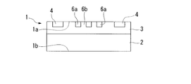
- FIG. 1 is a longitudinal sectional view showing a Schottky barrier diode which is an example of a semiconductor device of the present invention.
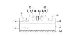
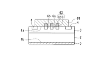
- FIG. 2A is a process diagram for explaining a method of manufacturing the Schottky barrier diode shown in FIG.
- FIG. 2B is a process diagram for explaining the manufacturing method of the Schottky barrier diode shown in FIG.
- FIG. 2C is a process diagram for describing the manufacturing method of the Schottky barrier diode shown in FIG. 1.
- FIG. 2D is a process diagram for describing the manufacturing method of the Schottky barrier diode shown in FIG. 1.
- FIG. 2E is a process diagram for describing the manufacturing method of the Schottky barrier diode shown in FIG. 1.
- FIG. 1 is a longitudinal sectional view showing a Schottky barrier diode which is an example of a semiconductor device of the present invention.
- FIG. 2A is a process diagram for explaining a method of manufacturing the Schottky barrier di
- FIG. 3A is an optical micrograph of an example showing pattern formation of an ohmic junction layer of a Schottky barrier diode.
- FIG. 3B is an optical micrograph of a comparative example showing pattern formation of an ohmic junction layer of a Schottky barrier diode.
- FIG. 1 is a longitudinal sectional view showing a Schottky barrier diode which is an example of a semiconductor device of the present invention.
- the Schottky barrier diode shown in FIG. 1 includes a SiC semiconductor substrate 1, a cathode electrode 5, an ohmic junction layer 7, and a Schottky junction layer 8.
- An SiC semiconductor substrate 1 shown in FIG. 1 is of an n type, and includes an n + type SiC layer 2 and an n ⁇ type SiC layer 3.
- the n + type SiC layer 2 is made of a low resistance n + type 4H—SiC single crystal substrate.
- the impurity concentration of the n + -type SiC layer 2 can be arbitrarily selected, but is preferably about 2 ⁇ 10 18 cm ⁇ 3 . Further, the thickness of the n + -type SiC layer 2 can be arbitrarily selected, but is preferably about 350 ⁇ m.
- the n ⁇ type SiC layer 3 is an n ⁇ type epitaxial layer formed on the n + type SiC layer 2.
- the impurity concentration of n ⁇ type SiC layer 3 is preferably about 1 ⁇ 10 16 cm ⁇ 3 .
- the thickness of the n ⁇ -type SiC layer 3 is preferably about 8 ⁇ m.
- the SiC semiconductor substrate 1 n - -type top surface 1a is SiC layer 3 side of the surface (the other main surface) has a plurality of first semiconductor regions 6a made of p + -type SiC, guard rings of p + -type SiC 4, and a second semiconductor region 6 b made of the surface of the n ⁇ -type SiC layer 3 disposed between the first semiconductor regions 6 a and between the first semiconductor region 6 a and the guard ring 4.
- the first semiconductor region 6a is p + type SiC formed by ion implantation of aluminum. As shown in FIG. 1, a plurality of first semiconductor regions 6a may be provided on the surface (upper surface 1a) on the n ⁇ -type SiC layer 3 side, or only one location may be provided. Further, the planar shape of the first semiconductor region 6a is not particularly limited, and may be, for example, a linear shape, an island shape, or a mesh shape.
- the guard ring 4 is arranged in an annular shape so as to surround the first semiconductor region 6a on the surface (the other main surface) on the n ⁇ -type SiC layer 3 side of the SiC semiconductor substrate 1, and in a plan view, the guard ring 4 It is formed so that it may straddle the peripheral part.
- the guard ring 4 relaxes electric field concentration at the peripheral portion of the Schottky junction layer 8.
- the guard ring 4 is p + type SiC formed by ion implantation of aluminum, like the first semiconductor region 6a.
- the concentration of aluminum ions constituting the p + -type SiC and the depth at which aluminum is ion-implanted may be the same or different. These values can also be arbitrarily selected.
- the ion implantation amount of aluminum ions constituting the p + type SiC of the first semiconductor region 6a and the guard ring 4 can be about 1 ⁇ 10 15 cm ⁇ 2 ,
- the depth of implantation can be about 300 nm.
- the ohmic junction layer 7 is an electrode that is in ohmic contact with the p + -type SiC constituting the first semiconductor region 6a.
- the ohmic junction layer 7 may be in ohmic contact with only a part of the first semiconductor region 6a, or may be in ohmic contact with the entire first semiconductor region 6a.
- the thickness of the ohmic junction layer 7 can be arbitrarily selected, but is preferably in the range of 50 nm to 200 nm, and more preferably about 130 nm.
- the ohmic bonding layer 7 is made of an alloy containing titanium and nickel, contains nickel in a weight composition ratio of 80 wt% or more and less than 95 wt%, and contains nickel in a weight composition ratio of 85 wt% or more and less than 90 wt%. Is more preferable. If the weight composition ratio of nickel is less than 80 wt% and the weight composition ratio of nickel exceeds 95 wt%, the ohmic junction layer 7 may not have a sufficiently low resistance value.
- the amount of titanium in the alloy is arbitrarily selected, it is preferably contained in a weight composition ratio of 5 wt% or more and less than 20 wt%.
- the alloy containing titanium and nickel may be composed only of titanium and nickel, but in addition to nickel having a weight composition ratio of 80 wt% or more and less than 95 wt%, and titanium, Si, C, etc. It may contain an element.
- the Schottky junction layer 8 is an electrode that is in Schottky contact with the n ⁇ -type SiC layer 3 constituting the second semiconductor region 6b. Further, the Schottky junction layer 8 is electrically connected to the ohmic junction layer 7.
- the Schottky bonding layer 8 is provided so as to cover the entire inner side of the guard ring 4, and the peripheral edge overlaps the guard ring 4 in plan view.
- the Schottky junction layer 8 is made of a metal whose main component is molybdenum. Examples of the metal having molybdenum as a main component include molybdenum alone, and metals (alloys) containing Ni, Ti, W, Ta, Pt, and the like. Specific examples include MoTi and MoNi.
- a cathode electrode 5 is provided on the lower surface 1 b which is the surface (one main surface) of the SiC semiconductor substrate 1 on the n + -type SiC layer 2 side. Cathode electrode 5 is in ohmic contact with n + -type SiC layer 2.
- the cathode electrode 5 is made of a metal whose main component is nickel. Examples of the metal having nickel as a main component include nickel (Ni), metals (alloys) containing Ti, Al, and the like. Specific examples include NiAl and NiTi.
- the thickness of the cathode electrode 5 is not particularly limited, but is preferably about 100 nm.
- FIGS. 2A to 2E are process diagrams for explaining a method of manufacturing the Schottky barrier diode shown in FIG.
- the Schottky barrier diode shown in FIG. 1 first, on the n + -type SiC layer 2, n - stacked type epitaxial layer n - -type SiC layer 3, the n + -type SiC layer 2 And an n ⁇ type SiC layer 3.
- the SiC semiconductor substrate 1 is introduced into a high-temperature heating furnace, and heat treatment is performed, for example, at a temperature of 1800 ° C. for 3 minutes, whereby ions are implanted into the guard ring 4 and the first semiconductor region 6a. Activates aluminum ions.
- the surface (lower surface 1b) on the n + -type SiC layer 2 side of the SiC semiconductor substrate 1 is made of a metal mainly composed of nickel by using an electron beam (EB) vapor deposition method or the like.
- the first metal layer 51 to be formed is formed to have a thickness of 100 nm, for example.
- the SiC semiconductor substrate 1 on which the first metal layer 51 is formed is introduced into a high-temperature heating furnace, and heat treatment is performed at a temperature of 900 ° C. or higher and lower than 1100 ° C. for 1 minute to 5 minutes in an atmospheric pressure argon gas atmosphere.
- the first metal layer 51 is alloyed (alloying heat treatment). This forms a cathode electrode 5 in ohmic contact with the n + -type SiC layer 2 as shown in FIG. 2B.
- the first semiconductor region 6a is formed on the first semiconductor region 6a of the n ⁇ -type SiC layer 3 using a pattern having a shape corresponding to the ohmic junction layer 7 drawn by the photolithography process.
- a laminated structure is formed by providing a titanium layer 61 and a nickel layer 62 in this order by an electron beam (EB) vapor deposition method or the like over the entire upper region, and nickel is contained in a weight composition ratio of 80 wt% or more and less than 95 wt%.
- a metal layer 63 is formed.
- the weight composition ratio of nickel contained in the second metal layer 63 can be adjusted by adjusting the thickness of each layer constituting the second metal layer 63.
- the stacking order of the titanium layer 61 and the nickel layer 62 in the stacked structure constituting the second metal layer 63 is not particularly limited, and the titanium layer 61 may be formed first, or the nickel layer 62 may be formed. It may be formed first.
- a third metal layer 81 is formed on the second semiconductor region 6b of the n ⁇ -type SiC layer 3 so as to cover the second metal layer 63 as well.
- the formation of the third metal layer 81 is performed using a pattern having a shape corresponding to the Schottky junction layer 8 drawn by a photolithography process, and a metal mainly composed of molybdenum is guarded by an electron beam (EB) evaporation method or the like. It is formed so as to cover the entire inner side of the ring 4 and the peripheral edge overlaps with the guard ring 4 in plan view.
- EB electron beam
- the SiC semiconductor substrate 1 on which the second metal layer 63 and the third metal layer 81 are formed is introduced into a high-temperature heating furnace, and the second metal is introduced in an argon gas atmosphere at atmospheric pressure.
- the layer 63 and the third metal layer 81 are alloyed.
- the ohmic junction layer 7 that makes ohmic contact with the first semiconductor region 6a and the Schottky junction layer 8 that makes Schottky junction with the second semiconductor region 6b can be formed simultaneously.
- the alloying temperature of the second metal (second metal layer 63) and the third metal (third metal layer 81) is lower than the temperature at which the first metal layer 51 is alloyed, specifically 500 ° C. or more. It is preferable to use a temperature lower than 900 ° C., and a temperature of 600 ° C. or higher and lower than 700 ° C. is more preferable. Moreover, it is preferable to perform the heat processing for about 5 minutes for the time of alloying, for example.
- the temperature at which the second metal layer 63 to be the ohmic junction layer 7 is alloyed is less than 500 ° C., the resistance value of the ohmic junction layer 7 may not be sufficiently low. Further, if the temperature at which the second metal layer 63 is alloyed is 900 ° C. or higher, the surface flatness of the ohmic bonding layer 7 is deteriorated and the mean square roughness may not be sufficiently low.
- the case where the second metal layer 63 and the third metal layer 81 are alloyed at the same time has been described as an example, but they may be separately alloyed.
- the SiC semiconductor substrate 1 on which the second metal layer 63 is formed is introduced into a high-temperature heating furnace, and is 500 ° C. or higher in an argon gas atmosphere at atmospheric pressure.
- the second metal layer 63 is alloyed (alloying heat treatment) by performing a heat treatment at a temperature lower than 900 ° C. for 1 minute to 5 minutes. In this way, the ohmic junction layer 7 is formed.
- the third metal layer 81 is introduced into a high temperature heating furnace and subjected to a heat treatment at a temperature of 500 ° C. or higher and lower than 900 ° C., for example, for 5 minutes to 20 minutes. Alloing. In this way, the Schottky junction layer 8 can be formed. Through the above process, the Schottky barrier diode shown in FIG. 1 is obtained.
- the ohmic junction layer 7 made of an alloy containing titanium and nickel is provided, the ohmic junction layer 7 and the first semiconductor region 6a The composition uniformity at the interface is excellent, and the first semiconductor region 6a is in ohmic contact well.
- the ohmic bonding layer 7 does not contain aluminum in the composition, the aluminum does not melt and aggregate during alloying, and the surface flatness of the ohmic bonding layer 7 is excellent, and the electrode pattern formation is excellent. A Schottky barrier diode is obtained.
- the Schottky connection layer 8 is made of a metal whose main component is molybdenum, sufficiently high adhesion between the ohmic junction layer 7 and the Schottky junction layer 8 can be obtained, and a reverse leakage current is obtained. And has excellent electrical characteristics with a large forward surge resistance.
- the ohmic junction layer 7 is made of an alloy containing titanium and nickel
- the cathode electrode 5 is made of a metal whose main component is nickel.
- the ohmic junction layer 7 and the Schottky junction layer 8 are formed by simultaneously performing heat treatment on the ohmic junction layer 7 that makes ohmic contact with the first semiconductor region 6a and the Schottky junction layer 8 that makes Schottky junction with the second semiconductor region 6b. Can be formed simultaneously. Therefore, a manufacturing process can be simplified compared with the case where the 2nd metal layer 63 and the 3rd metal layer 81 are each alloyed separately.
- the step of forming the second metal layer 63 including the titanium layer 61 and the nickel layer 62 on the first semiconductor region 6a includes a step of forming the ohmic junction layer 7 by alloying and a step of forming the third metal layer 81 on the second semiconductor region 6b and forming the Schottky junction layer 8 by alloying. Since the second metal layer 63 does not contain aluminum that melts and aggregates during alloying, a Schottky barrier diode with excellent surface flatness of the ohmic junction layer 7 and excellent electrode pattern formation is manufactured. can do.
- the second metal layer 63 to be the ohmic junction layer 7 includes the titanium layer 61 and the nickel layer 62, and the second metal layer 63 has a weight composition ratio of 85 wt% or more and less than 95 wt% of nickel.
- the resistance value of the ohmic bonding layer 7 is sufficiently low without containing aluminum that is melted by alloying.
- the manufacturing method of the Schottky barrier diode according to the present embodiment the aggregation of the metal composition contained in the second metal layer 63 is prevented. It is possible to manufacture a Schottky barrier diode including the ohmic junction layer 7 which is excellent in the above and provides sufficiently high adhesion with the Schottky junction layer 8.
- the alloying of the second metal layer 63 is performed at a temperature of 500 ° C. or higher and lower than 900 ° C., the resistance value is sufficiently low and the surface flatness is excellent.
- the ohmic junction layer 7 is obtained.
- the second metal layer 63 contains nickel in a weight composition ratio of 80 wt% or more and less than 95 wt%, the ohmic junction having further excellent surface flatness. Layer 7 is obtained.
- the Schottky junction layer 8 is formed of a metal whose main component is molybdenum, the temperature is approximately the same as the temperature at which the second metal layer 63 is alloyed.
- the Schottky junction layer 8 can be formed by alloying the third metal layer 81 at a temperature. Further, the temperature for alloying the third metal layer can be lower than the temperature for alloying the second metal layer.
- the method of forming the first metal layer 51, the second metal layer 63, and the third metal layer 81 is not limited to the electron beam (EB) vapor deposition method, and a sputtering method, a resistance heating method, or the like may be used. Good.
- EB electron beam
- a sputtering method, a resistance heating method, or the like may be used.
- the crystal polymorph of the SiC single crystal substrate constituting the n + -type SiC layer 2 is not limited to 4H—SiC, and may be 6H—SiC or 3H—SiC.
- the first metal layer 51 and the second metal layer 63 are alloyed in an argon atmospheric pressure, but may be in a nitrogen atmosphere or in a vacuum. Moreover, you may perform the alloying of the 1st metal layer 51 and the 2nd metal layer 63 in argon atmosphere by the rapid thermal processing (Rapid Thermal Annealing: RTA) method.
- Example 1 The Schottky barrier diode shown in FIG. 1 was manufactured as follows. First, an n ⁇ type epitaxial layer is stacked on an n + type SiC layer 2 having a thickness of 350 ⁇ m to form an n ⁇ type SiC layer 3 having a thickness of 8 ⁇ m, and an impurity comprising an n + type 4H—SiC single crystal substrate. An n-type SiC semiconductor substrate 1 including an n + -type SiC layer 2 having a concentration of 2 ⁇ 10 18 cm ⁇ 3 and an n ⁇ -type SiC layer 3 having an impurity concentration of 1 ⁇ 10 16 cm ⁇ 3 was obtained.
- n - on the type SiC layer 3 using a plasma CVD apparatus to form a SiO 2 film having a thickness of 2 [mu] m draws a pattern by a photolithography process, by removing a portion of SiO 2 film, n -
- the region to be the guard ring 4 and the first semiconductor region 6a on the type SiC layer 3 is exposed, and aluminum is ion-implanted with an ion implantation amount of 1 ⁇ 10 15 cm ⁇ 2 and a depth of 300 nm, and p + -type SiC and did.
- first semiconductor regions 6a, a guard ring 4, and a plurality of second semiconductor regions 6b were formed on the upper surface 1a of the n ⁇ type SiC layer 3 of the SiC semiconductor substrate 1. Thereafter, the SiO 2 film was removed, the SiC semiconductor substrate 1 was introduced into a high-temperature heating furnace, and heat treatment was performed at a temperature of 1800 ° C. for 3 minutes, whereby ions were implanted into the guard ring 4 and the first semiconductor region 6a. Aluminum ions were activated.
- a first metal layer 51 made of nickel was formed on the surface (lower surface 1b) on the n + -type SiC layer 2 side of the SiC semiconductor substrate 1 by using an electron beam (EB) vapor deposition method.
- the SiC semiconductor substrate 1 on which the first metal layer 51 is formed is introduced into a high-temperature heating furnace, and heat treatment is performed at a temperature of 1000 ° C. for 3 minutes in an argon gas atmosphere at atmospheric pressure. Layer 51 was alloyed. As a result, a cathode electrode 5 having a thickness of 100 nm was formed.
- a pattern having a shape corresponding to the ohmic junction layer 7 drawn by the photolithography process is formed on the first semiconductor region 6a of the n ⁇ -type SiC layer 3 by an electron beam (EB) vapor deposition method.
- a second metal layer 63 was formed.
- the SiC semiconductor substrate 1 on which the second metal layer 63 is formed is introduced into a high-temperature heating furnace, and heat treatment is performed at a temperature of 700 ° C. for 5 minutes in an atmospheric pressure argon gas atmosphere. Layer 63 was alloyed. As a result, an ohmic junction layer 7 having a thickness of 130 nm was formed.
- a pattern having a shape corresponding to the Schottky junction layer 8 drawn by the photolithography process is used to form molybdenum from the molybdenum by an electron beam (EB) vapor deposition method.
- EB electron beam
- a third metal layer 81 that covers the entire inner side of the guard ring 4 and whose peripheral edge overlaps the guard ring 4 in plan view is formed.
- the SiC semiconductor substrate 1 on which the third metal layer 81 was formed was introduced into a high-temperature heating furnace, and heat treatment was performed at a temperature of 600 ° C. for 10 minutes, whereby the third metal layer 81 was alloyed.
- the Schottky junction layer 8 was formed, and the Schottky barrier diode of Example 1 was obtained.
- Example 2 The Schottky barrier diode shown in FIG. 1 was manufactured as follows. First, an n ⁇ type epitaxial layer is stacked on an n + type SiC layer 2 having a thickness of 350 ⁇ m to form an n ⁇ type SiC layer 3 having a thickness of 8 ⁇ m, and an impurity comprising an n + type 4H—SiC single crystal substrate. An n-type SiC semiconductor substrate 1 including an n + -type SiC layer 2 having a concentration of 2 ⁇ 10 18 cm ⁇ 3 and an n ⁇ -type SiC layer 3 having an impurity concentration of 1 ⁇ 10 16 cm ⁇ 3 was obtained.
- n - on the type SiC layer 3 using a plasma CVD apparatus to form a SiO 2 film having a thickness of 2 [mu] m draws a pattern by a photolithography process, by removing a portion of SiO 2 film, n -
- the region to be the guard ring 4 and the first semiconductor region 6a on the type SiC layer 3 is exposed, and aluminum is ion-implanted with an ion implantation amount of 1 ⁇ 10 15 cm ⁇ 2 and a depth of 300 nm, and p + -type SiC and did.
- first semiconductor regions 6a, a guard ring 4, and a plurality of second semiconductor regions 6b were formed on the upper surface 1a of the n ⁇ type SiC layer 3 of the SiC semiconductor substrate 1. Thereafter, the SiO 2 film was removed, the SiC semiconductor substrate 1 was introduced into a high-temperature heating furnace, and heat treatment was performed at a temperature of 1800 ° C. for 3 minutes, whereby ions were implanted into the guard ring 4 and the first semiconductor region 6a. Aluminum ions were activated.
- a first metal layer 51 made of nickel was formed on the surface (lower surface 1b) on the n + -type SiC layer 2 side of the SiC semiconductor substrate 1 by using an electron beam (EB) vapor deposition method.
- the SiC semiconductor substrate 1 on which the first metal layer 51 is formed is introduced into a high-temperature heating furnace, and heat treatment is performed at a temperature of 1000 ° C. for 3 minutes in an argon gas atmosphere at atmospheric pressure. Layer 51 alloyed. As a result, a cathode electrode 5 having a thickness of 100 nm was formed.
- a pattern having a shape corresponding to the ohmic junction layer 7 drawn by the photolithography process is formed on the first semiconductor region 6a of the n ⁇ -type SiC layer 3 by an electron beam (EB) vapor deposition method.
- EB electron beam
- a second metal layer 63 was formed.
- a pattern having a shape corresponding to the Schottky junction layer 8 drawn by the photolithography process is used to form molybdenum from the molybdenum by an electron beam (EB) vapor deposition method.
- EB electron beam
- the SiC semiconductor substrate 1 on which the second metal layer 63 and the third metal layer 81 are formed is introduced into a high-temperature heating furnace, and heat treatment is performed at a temperature of 650 ° C. for 10 minutes, whereby the second metal layer 63 And the 3rd metal layer 81 was alloyed simultaneously.
- an ohmic junction layer 7 and a Schottky junction layer 8 having a thickness of 130 nm were formed, and the Schottky barrier diode of Example 2 was obtained.
- the comparative Schottky barrier diode was obtained in the same manner as in the example except that the alloying temperature was set to 900 ° C. and an ohmic junction layer having a thickness of 120 nm was formed.
- FIGS. 3A and 3B are optical micrographs of the ohmic junction layer of the Schottky barrier diode.
- FIG. 3A is Example 1
- FIG. 3B is a comparative example.
- Example 2 also had a shape similar to that of Example 1.
- FIGS. 3A and 3B in the example, a pattern having excellent straightness is formed, but in the comparative example, there are many irregularities and the surface is rough, and it is understood that the straightness is deteriorated.
- a semiconductor device including an ohmic junction layer that has excellent surface flatness and excellent electrode pattern formation.
Landscapes
- Electrodes Of Semiconductors (AREA)
Abstract
n型のSiC半導体基体(1)と、SiC半導体基体(1)の一方の主表面(1b)とオーミック接触するカソード電極(5)と、SiC半導体基体(1)の他方の主表面(1a)に形成されたp型SiCからなる第1半導体領域(6a)と、他方の主表面(1a)に形成されたn型SiCからなる第2半導体領域(6b)と、第1半導体領域(6a)にオーミック接触するオーミック接合層(7)と、第2半導体領域(6b)にショットキー接触するショットキー接合層(8)と、を備え、オーミック接合層(7)が、第1半導体領域(6a)側からチタンとニッケルとを含む合金からなると共に、その上にモリブデンを主成分とする金属層を有し、ショットキー接続層(8)が、モリブデンを主成分とする金属からなることを特徴とする半導体装置である。
Description
本発明は、半導体装置および半導体装置の製造方法の改良に関する。
本願は、2010年2月9日に、日本に出願された特願2010-026816号に基づき優先権を主張し、その内容をここに援用する。
本願は、2010年2月9日に、日本に出願された特願2010-026816号に基づき優先権を主張し、その内容をここに援用する。
従来から、SiCショットキーバリアダイオードは、順方向にサージ電流が流れた際に、比較的低いサージ電流でも素子破壊が引き起こされることが知られている。この問題を解決するために、SiC半導体素子の一つの表面にn型領域とp型領域とを並列に配置し、大電流導通時にp型領域から少数キャリアである正孔の注入が起こるようにした素子構造が提案されている(例えば、非特許文献1参照)。このような素子構造とした場合、サージ耐量を向上させることができる。
このような素子構造は、MPS(Merged p-i-n Schottky)構造と呼ばれている。MPS構造では、半導体素子の一方の表面にショットキーダイオードとpn型ダイオードとを交互に配置している。したがって、半導体素子の一方の表面上には、n型半導体領域に良好なショットキー接合し、かつp型半導体領域に良好なオーミック接合をする接合材料からなる接合層を設ける必要がある。
n型半導体領域にショットキー接合をする接合層と、p型半導体領域にオーミック接合をする接合層とを同一材料で同時に形成する場合、これらをそれぞれ異なる材料で別々に形成する場合と比較して、製造工程を簡素化することができるため、好ましい。
このような接合層に用いられる接合材料としては、NiAl合金(例えば、特許文献1参照)や、TiNi合金(例えば、非特許文献2参照)が知られている。しかしながら、接合層としてNiAl合金やTiNi合金からなるものを用いた場合、ショットキー接合する均質な接合層を形成することは困難であった。それは以下のような理由によるものと考察される。
このような接合層に用いられる接合材料としては、NiAl合金(例えば、特許文献1参照)や、TiNi合金(例えば、非特許文献2参照)が知られている。しかしながら、接合層としてNiAl合金やTiNi合金からなるものを用いた場合、ショットキー接合する均質な接合層を形成することは困難であった。それは以下のような理由によるものと考察される。
例えば、半導体基体としてSiCからなるものを用い、半導体基体のn型半導体領域上にショットキー接合するNiAl合金あるいはTiNi合金からなる接合層を形成する場合、通常、n型半導体領域上にNiAl合金あるいはTiNi合金となる金属層を形成し、高温でアロイングすることにより形成する。このようにして接合層を形成する場合、n型半導体領域を構成するSiCと、接合層を構成するNiAl合金あるいはTiNi合金との界面において、NiAl合金に含まれるNiとAlとの組成、あるいは、TiNi合金に含まれるTiとNiとの組成が不均一になりやすく、ショットキー接合する接合層内にバリアハイトの不均一な領域が生じてしまう場合があった。このため、このような方法で製造されたショットキーバリアダイオードに逆方向電圧を印加すると、ショットキーバリアの低い領域でリーク電流の増大が観察され、十分な電気的特性が得られない場合があった。
ショットキー接合する合金とn型半導体領域との界面における合金組成の不均一に起因する問題を解決するには、ショットキー接合する接合層として単一元素の金属を用いることが望ましい。しかし、現在まで、n型半導体領域に良好なショットキー接合をし、なおかつp型半導体領域に良好なオーミック接合をする単一元素の金属は発見されていない。
したがって、n型半導体領域に良好なショットキー接合をし、かつp型半導体領域に良好なオーミック接合をする接合層とするために、n型半導体領域に良好なショットキー接合をするショットキー接合層と、p型半導体領域に良好なオーミック接合をするオーミック接合層とをそれぞれ異なる材料で形成することが考えられる。
例えば、p型SiC半導体基体に対するオーミック電極としては、TiとAlとを順に成膜して熱処理することにより得られたものがある(例えば、特許文献2参照)。また、特許文献2には、ニッケルとシリコンと炭素とアルミニウムとを含むオーミック電極構造も記載されている。
例えば、p型SiC半導体基体に対するオーミック電極としては、TiとAlとを順に成膜して熱処理することにより得られたものがある(例えば、特許文献2参照)。また、特許文献2には、ニッケルとシリコンと炭素とアルミニウムとを含むオーミック電極構造も記載されている。
Analysis of a High-Voltage Merged p-i-n/Schottky (MPS) Rectifier:IEEE Electron Device Letters,Vol.Edl8;No.9,September 1987:p407-409
Diamond & Related Materials 14 (2005)1146-1149
しかしながら、p型半導体領域上にAlを含む合金金属層を形成し、良好なオーミック接触が得られるオーミック接合層とするためには900℃以上でアロイングする必要がある。このような高温でアロイングを行うことにより約660℃と融点の低いアルミニウムが融けて凝集するため、表面に凹凸が生じて表面が荒れることが問題となっている。
例えば、特許文献1には、TiとAlとの膜が、熱処理により表面に凹凸が生じると、電極周辺にTiAl合金がはみ出してしまい、電極のパターン形成が困難になることが示されている。このように、電極のパターン形成が狙い通りに出来ないと、半導体素子の微細化が実施できないという問題があった。
また、表面に凹凸を有するオーミック接合層では、SiCからなる半導体基体との界面においてオーミック接合層に含まれる合金の組成が不均一となっていることにより、電気的特性の劣化が引き起こされる。
また、MPS構造のSiCショットキーダイオードを大電流で使用する場合、オーミック接合層は、ショットキー接合層との界面における低い抵抗値や安定性が要求されるとともに、その上に積層されるショットキー接合層との高い密着性が要求される。しかし、表面の荒れたオーミック接合層は、その上に積層されるショットキー接合層との間に空隙が生じやすいものであるため、ショットキー接合層との十分に高い密着性が得られない場合があった。
さらに、SiC半導体素子では、一般的に電気的特性を向上させるために、カソード電極とアノード電極とをそれぞれ異なる温度で個別にアロイングする必要があるが、オーミック電極を個別に形成することで、さらにアロイ工程が一回増加することとなり、工程が複雑化してしまうという問題があった。
本発明は、上記事情に鑑みてなされたもので、表面平坦性に優れ、電極のパターン形成性に優れるオーミック接合層を備える半導体装置を提供することを目的とする。
また、本発明は、熱処理工程の簡素化が可能な本発明の半導体装置の製造方法を提供することを目的とする。
また、本発明は、熱処理工程の簡素化が可能な本発明の半導体装置の製造方法を提供することを目的とする。
上記の目的を達成するために、本発明は以下の構成を採用した。
[1] n型のSiC半導体基体と、
前記SiC半導体基体の一方の主表面とオーミック接触するカソード電極と、
前記SiC半導体基体の他方の主表面に形成されたp型SiCからなる第1半導体領域と、
前記他方の主表面に形成されたn型SiCからなる第2半導体領域と、
前記第1半導体領域にオーミック接触するオーミック接合層と、
前記第2半導体領域にショットキー接触するショットキー接合層と、を備え、
前記オーミック接合層が、前記第1半導体領域側からチタンとニッケルとを含む合金からなると共に、その上にモリブデンを主成分とする金属層を有し、
前記ショットキー接続層が、モリブデンを主成分とする金属からなることを特徴とする半導体装置。
[2] 前記カソード電極が、ニッケルを主成分とする金属からなることを特徴とする前項1に記載の半導体装置。
[3] 前記合金が、ニッケルを重量組成比で80wt%以上95wt%未満含むものであることを特徴とする前項1又は前項2に記載の半導体装置。
[4] 一方の主表面と他方の主表面とを備え、前記他方の主表面にp型SiCからなる第1半導体領域とn型SiCからなる第2半導体領域とが設けられたn型のSiC半導体基体を形成する工程と、
前記一方の主表面上に、第1金属層を形成する工程と、
前記第1金属層をアロイングすることにより、前記一方の主表面とオーミック接触するカソード電極を形成する工程と、
前記第1半導体領域上に、チタン層とニッケル層とを含む第2金属層を形成する工程と、
前記第2金属層をアロイングすることにより、前記第1半導体領域とオーミック接合するオーミック接合層を形成する工程と、
前記第2半導体領域上に、第3金属層を形成する工程と、
前記第3金属層をアロイングすることにより、前記第2半導体領域とショットキー接合するショットキー接合層を形成する工程と、を含むことを特徴とする半導体装置の製造方法。
[5] 前記第2金属層が、ニッケルを重量組成比で80wt%以上95wt%未満含む組成であることを特徴とする前項4に記載の半導体装置の製造方法。
[6] 前記第2金属層を形成する工程が、前記第1半導体領域上に金属チタン層を形成した後に、前記金属チタン層上に金属ニッケル層を形成することを特徴とする前項4又は前項5に記載の半導体装置の製造方法
[7] 前記第2金属層及び前記第3金属層のアロイングを、500℃以上900℃未満の温度で行うことを特徴とする前項4乃至6のいずれか一項に記載の半導体装置の製造方法。
[8] 前記第2金属層をアロイングする工程と、前記第3金属層をアロイングする工程とを同時に行うことを特徴とする前項4乃至7のいずれか一項に記載の半導体装置の製造方法。
[9] 前記カソード電極を、ニッケルを主成分とする金属で形成することを特徴とする前項4乃至8のいずれか一項に記載の半導体装置の製造方法。
[10] 前記第3金属層を、モリブデンを主成分とする金属で形成することを特徴とする前項4乃至9のいずれか一項に記載の半導体装置の製造方法。
[1] n型のSiC半導体基体と、
前記SiC半導体基体の一方の主表面とオーミック接触するカソード電極と、
前記SiC半導体基体の他方の主表面に形成されたp型SiCからなる第1半導体領域と、
前記他方の主表面に形成されたn型SiCからなる第2半導体領域と、
前記第1半導体領域にオーミック接触するオーミック接合層と、
前記第2半導体領域にショットキー接触するショットキー接合層と、を備え、
前記オーミック接合層が、前記第1半導体領域側からチタンとニッケルとを含む合金からなると共に、その上にモリブデンを主成分とする金属層を有し、
前記ショットキー接続層が、モリブデンを主成分とする金属からなることを特徴とする半導体装置。
[2] 前記カソード電極が、ニッケルを主成分とする金属からなることを特徴とする前項1に記載の半導体装置。
[3] 前記合金が、ニッケルを重量組成比で80wt%以上95wt%未満含むものであることを特徴とする前項1又は前項2に記載の半導体装置。
[4] 一方の主表面と他方の主表面とを備え、前記他方の主表面にp型SiCからなる第1半導体領域とn型SiCからなる第2半導体領域とが設けられたn型のSiC半導体基体を形成する工程と、
前記一方の主表面上に、第1金属層を形成する工程と、
前記第1金属層をアロイングすることにより、前記一方の主表面とオーミック接触するカソード電極を形成する工程と、
前記第1半導体領域上に、チタン層とニッケル層とを含む第2金属層を形成する工程と、
前記第2金属層をアロイングすることにより、前記第1半導体領域とオーミック接合するオーミック接合層を形成する工程と、
前記第2半導体領域上に、第3金属層を形成する工程と、
前記第3金属層をアロイングすることにより、前記第2半導体領域とショットキー接合するショットキー接合層を形成する工程と、を含むことを特徴とする半導体装置の製造方法。
[5] 前記第2金属層が、ニッケルを重量組成比で80wt%以上95wt%未満含む組成であることを特徴とする前項4に記載の半導体装置の製造方法。
[6] 前記第2金属層を形成する工程が、前記第1半導体領域上に金属チタン層を形成した後に、前記金属チタン層上に金属ニッケル層を形成することを特徴とする前項4又は前項5に記載の半導体装置の製造方法
[7] 前記第2金属層及び前記第3金属層のアロイングを、500℃以上900℃未満の温度で行うことを特徴とする前項4乃至6のいずれか一項に記載の半導体装置の製造方法。
[8] 前記第2金属層をアロイングする工程と、前記第3金属層をアロイングする工程とを同時に行うことを特徴とする前項4乃至7のいずれか一項に記載の半導体装置の製造方法。
[9] 前記カソード電極を、ニッケルを主成分とする金属で形成することを特徴とする前項4乃至8のいずれか一項に記載の半導体装置の製造方法。
[10] 前記第3金属層を、モリブデンを主成分とする金属で形成することを特徴とする前項4乃至9のいずれか一項に記載の半導体装置の製造方法。
本発明の半導体装置によれば、オーミック接合層が、第1半導体領域側からチタンとニッケルとを含む合金からなり、その上にモリブデンを主成分とする金属層を有しているので、オーミック接合層と第1半導体領域との界面における組成の均一性に優れ、第1半導体領域と良好にオーミック接合するものとなる。また、組成中にアルミニウムを含まないため、アロイングの際にアルミニウムが溶融して凝集することがないため、オーミック接合層の表面平坦性に優れ、電極のパターン形成性に優れる半導体装置を提供することができる。
また、ショットキー接続層がモリブデンを主成分とする金属からなるものであるので、オーミック接合層とショットキー接合層との間で、十分に高い密着性が得られるものとなるため、逆方向のリーク電流が低く、順方向サージ耐量が大きい優れた電気的特性を有するものとなる。
また、ショットキー接続層がモリブデンを主成分とする金属からなるものであるので、オーミック接合層とショットキー接合層との間で、十分に高い密着性が得られるものとなるため、逆方向のリーク電流が低く、順方向サージ耐量が大きい優れた電気的特性を有するものとなる。
また、本発明の半導体装置の製造方法は、第1半導体領域上に、チタン層とニッケル層とを含む第2金属層を形成する工程と、第2金属層をアロイングすることにより、前記第1半導体領域とオーミック接合するオーミック接合層を形成する工程と、第2半導体領域上に、第3金属層を形成する工程と、前記第3金属層をアロイングすることにより、第2半導体領域とショットキー接合するショットキー接合層を形成する工程とを含み、第2金属層にアルミニウムが含まれない構成となっている。このため、第3金属層のアロイングの際に第2金属層が溶融して凝集することがない。このため、本発明の半導体装置の製造方法によれば、オーミック接合層の表面平坦性に優れ、電極のパターン形成性に優れる半導体装置を製造することができる。
さらに、第2金属層をアロイングする工程と、第3金属層をアロイングする工程とを同時に行う場合には、熱処理工程の簡素化を実現できる。
さらに、第2金属層をアロイングする工程と、第3金属層をアロイングする工程とを同時に行う場合には、熱処理工程の簡素化を実現できる。
以下、本発明を、図面を参照して詳細に説明する。なお、以下の説明において参照する図面に図示される各部の大きさや厚さや寸法等は、実際の半導体装置の寸法関係とは異なっている場合がある。また本発明は以下の例のみに限られるものではなく、本発明の要旨を逸脱しない範囲で、変更や追加や省略をする事ができる。
<半導体装置>
図1は、本発明の半導体装置の一例であるショットキーバリアダイオードを示した縦断面図である。図1に示すショットキーバリアダイオードは、SiC半導体基体1と、カソード電極5と、オーミック接合層7と、ショットキー接合層8とを備えたものである。
図1は、本発明の半導体装置の一例であるショットキーバリアダイオードを示した縦断面図である。図1に示すショットキーバリアダイオードは、SiC半導体基体1と、カソード電極5と、オーミック接合層7と、ショットキー接合層8とを備えたものである。
図1に示すSiC半導体基体1は、n型のものであり、n+型SiC層2とn-型SiC層3とを備えている。n+型SiC層2は、低抵抗のn+型4H-SiC単結晶基板からなる。n+型SiC層2の不純物濃度は任意で選択できるが、2×1018cm-3程度であることが好ましい。また、n+型SiC層2の厚さは任意で選択できるが、350μm程度であること好ましい。
n-型SiC層3は、n+型SiC層2上に形成されたn-型エピタキシャル層からなる。n-型SiC層3の不純物濃度は1×1016cm-3程度であることが好ましい。また、n-型SiC層3の厚さは、8μm程度であること好ましい。
n-型SiC層3は、n+型SiC層2上に形成されたn-型エピタキシャル層からなる。n-型SiC層3の不純物濃度は1×1016cm-3程度であることが好ましい。また、n-型SiC層3の厚さは、8μm程度であること好ましい。
SiC半導体基体1のn-型SiC層3側の表面(他方の主表面)である上面1aには、p+型SiCからなる複数の第1半導体領域6aと、p+型SiCからなるガードリング4と、第1半導体領域6a間および第1半導体領域6aとガードリング4との間に配置されたn-型SiC層3の表面からなる第2半導体領域6bとが備えられている。
第1半導体領域6aは、アルミニウムがイオン注入されることにより形成されたp+型SiCである。図1に示すように、第1半導体領域6aは、n-型SiC層3側の表面(上面1a)に複数個所設けてられていても良いが、一箇所のみ設けられていても良い。また、第1半導体領域6aの平面形状は、特に限定されるものではなく、例えば、線状、島状、網目状などの形状にすることができる。
ガードリング4は、SiC半導体基体1のn-型SiC層3側の表面(他方の主表面)上において、第1半導体領域6aを取り囲むように環状に配置され、平面視でショットキー接合層8の周縁部に跨るように形成されている。ガードリング4は、ショットキー接合層8の周縁部における電界集中を緩和するものである。ガードリング4は、第1半導体領域6aと同様に、アルミニウムがイオン注入されることにより形成されたp+型SiCである。
ガードリング4と第1半導体領域6aとにおいて、p+型SiCを構成するアルミニウムイオンの濃度やアルミニウムがイオン注入される深さは、同じであっても良いし、異なっていても良い。またこれら値も任意で選択できる。具体的例を挙げれば、例えば、第1半導体領域6aおよびガードリング4のp+型SiCを構成するアルミニウムイオンのイオン注入量は1×1015cm-2程度とすることができ、アルミニウムがイオン注入される深さは300nm程度とすることができる。
オーミック接合層7は、第1半導体領域6aを構成するp+型SiCにオーミック接触している電極である。オーミック接合層7は、第1半導体領域6aの一部にのみオーミック接触していても良いし、第1半導体領域6aの全部にオーミック接触していても良い。
オーミック接合層7の厚さは任意で選択できるが、50nm~200nmの範囲であることが望ましく、130nm程度であることがより望ましい。
オーミック接合層7の厚さは任意で選択できるが、50nm~200nmの範囲であることが望ましく、130nm程度であることがより望ましい。
また、オーミック接合層7は、チタンとニッケルとを含む合金からなり、ニッケルを重量組成比で80wt%以上95wt%未満含むものであり、ニッケルを重量組成比で85wt%以上90wt%未満含むものであることがより好ましい。ニッケルの重量組成比が、80wt%未満であると、またニッケルの重量組成比が、95wt%を超えると、オーミック接合層7の抵抗値が十分に低いものとならない恐れがある。前記合金のチタンの量は任意で選択されるが、重量組成比で5wt%以上20wt%未満含まれることが好ましい。
なお、チタンとニッケルとを含む合金は、チタンとニッケルのみからなるものであってもよいが、重量組成比で80wt%以上95wt%未満のニッケルと、チタンとに加えてさらにSi、Cなどの元素を含むものであってもよい。
なお、チタンとニッケルとを含む合金は、チタンとニッケルのみからなるものであってもよいが、重量組成比で80wt%以上95wt%未満のニッケルと、チタンとに加えてさらにSi、Cなどの元素を含むものであってもよい。
ショットキー接合層8は、第2半導体領域6bを構成するn-型SiC層3にショットキー接触している電極である。また、ショットキー接合層8は、オーミック接合層7と電気的に接続されている。ショットキー接合層8は、ガードリング4の内側全域を覆うように設けられており、周縁部がガードリング4と平面視で重なり合っている。
ショットキー接合層8は、モリブデンを主成分とする金属からなるものである。モリブデンを主成分とする金属としては、モリブデン単体の他、Ni、Ti、W、Ta、Ptなどを含む金属(合金)などが挙げられる。具体例を挙げればMoTi、及びMoNiなどがある。
ショットキー接合層8は、モリブデンを主成分とする金属からなるものである。モリブデンを主成分とする金属としては、モリブデン単体の他、Ni、Ti、W、Ta、Ptなどを含む金属(合金)などが挙げられる。具体例を挙げればMoTi、及びMoNiなどがある。
SiC半導体基体1のn+型SiC層2側の表面(一方の主表面)である下面1bには、カソード電極5が設けられている。カソード電極5は、n+型SiC層2にオーミック接触されている。
カソード電極5は、ニッケルを主成分とする金属からなるものである。ニッケルを主成分とする金属としては、ニッケル単体の他、Ti、Alなどを含む金属(合金)などが挙げられる。具体例を挙げればNiAl、及びNiTiなどがある。
また、カソード電極5の厚みは、特に限定されないが、100nm程度であることが好ましい。
カソード電極5は、ニッケルを主成分とする金属からなるものである。ニッケルを主成分とする金属としては、ニッケル単体の他、Ti、Alなどを含む金属(合金)などが挙げられる。具体例を挙げればNiAl、及びNiTiなどがある。
また、カソード電極5の厚みは、特に限定されないが、100nm程度であることが好ましい。
<半導体装置の製造方法>
次に、本発明の半導体装置の製造方法の一例として、図2Aから図2Eを用いて、図1に示すショットキーバリアダイオードの製造方法を説明する。図2Aから図2Eは、図1に示すショットキーバリアダイオードの製造方法を説明するための工程図である。
図1に示すショットキーバリアダイオードを製造するには、まず、n+型SiC層2上に、n-型エピタキシャル層を積層してn-型SiC層3を形成し、n+型SiC層2とn-型SiC層3とを備えるn型のSiC半導体基体1とする。
次に、本発明の半導体装置の製造方法の一例として、図2Aから図2Eを用いて、図1に示すショットキーバリアダイオードの製造方法を説明する。図2Aから図2Eは、図1に示すショットキーバリアダイオードの製造方法を説明するための工程図である。
図1に示すショットキーバリアダイオードを製造するには、まず、n+型SiC層2上に、n-型エピタキシャル層を積層してn-型SiC層3を形成し、n+型SiC層2とn-型SiC層3とを備えるn型のSiC半導体基体1とする。
次いで、n-型SiC層3上に、プラズマCVD装置を用いて例えば厚さ略2μmのSiO2膜を形成し、フォトリソグラフィー工程によりガードリング4および第1半導体領域6aに対応する形状のパターンを描画する。続いて、SiO2膜の一部を除去して、n-型SiC層3上のガードリング4および第1半導体領域6aとなる領域を露出させ、アルミニウムをイオン注入してp+型SiCとする。このことにより、図2Aに示すように、SiC半導体基体1の上面1aに、第1半導体領域6aと、ガードリング4と、第2半導体領域6bとが形成される。その後、SiO2膜を除去し、SiC半導体基体1を高温加熱炉内に導入し、例えば1800℃の温度で3分間の熱処理を行うことにより、ガードリング4および第1半導体領域6aにイオン注入されたアルミニウムイオンを活性化させる。
次に、図2Bに示すように、SiC半導体基体1のn+型SiC層2側の表面(下面1b)に、電子ビーム(EB)蒸着法などを用いて、ニッケルを主成分とする金属からなる第1金属層51を例えば厚さ100nmとなるように形成する。
次に、第1金属層51の形成されたSiC半導体基体1を高温加熱炉内に導入し、大気圧のアルゴンガス雰囲気中、900℃以上1100℃未満の温度で1分間~5分間の熱処理を行うことにより、第1金属層51をアロイング(合金化熱処理)する。このことにより、図2Bに示すように、n+型SiC層2とオーミック接触するカソード電極5を形成する。
次に、図2Cに示すように、n-型SiC層3の第1半導体領域6a上に、フォトリソグラフィー工程により描画したオーミック接合層7に対応する形状のパターンを用いて、第1半導体領域6a上の全域に電子ビーム(EB)蒸着法などにより、チタン層61とニッケル層62とをこの順で設けて積層構造を形成し、ニッケルが重量組成比で80wt%以上95wt%未満含まれる第2金属層63を形成する。第2金属層63に含まれるニッケルの重量組成比は、第2金属層63を構成する各層の厚みを調節することによって調整できる。
なお、第2金属層63を構成する積層構造におけるチタン層61とニッケル層62との積層順序は特に限定されるものではなく、チタン層61を先に形成してもよいし、ニッケル層62を先に形成してもよい。
なお、第2金属層63を構成する積層構造におけるチタン層61とニッケル層62との積層順序は特に限定されるものではなく、チタン層61を先に形成してもよいし、ニッケル層62を先に形成してもよい。
次に、図2Dに示すように、n-型SiC層3の第2半導体領域6b上に、第2金属層63も覆うように第3金属層81を形成する。この第3金属層81の形成は、フォトリソグラフィー工程により描画したショットキー接合層8に対応する形状のパターンを用いて、モリブデンを主成分とする金属を電子ビーム(EB)蒸着法などにより、ガードリング4の内側全域を覆い、周縁部がガードリング4と平面視で重なり合うようにして形成する。
次に、図2Eに示すように、第2金属層63及び第3金属層81の形成されたSiC半導体基体1を高温加熱炉内に導入し、大気圧のアルゴンガス雰囲気中で、第2金属層63及び第3金属層81をアロイングする。これにより、第1半導体領域6aとオーミック接合するオーミック接合層7と、第2半導体領域6bとショットキー接合するショットキー接合層8とを同時形成することができる。
第2の金属(第2金属層63)及び第3の金属(第3金属層81)のアロイングの温度は、第1金属層51をアロイングする温度よりも低い温度、具体的には500℃以上900℃未満の温度を用いることが好ましく、600度以上700度未満の温度がより好ましい。
また、アロイングの時間は、例えば5分間程度の熱処理を行うことが好ましい。
また、アロイングの時間は、例えば5分間程度の熱処理を行うことが好ましい。
ここで、オーミック接合層7となる第2金属層63をアロイングする温度が500℃未満であると、オーミック接合層7の抵抗値が十分に低いものとならない恐れがある。また、第2金属層63をアロイングする温度が900℃以上であると、オーミック接合層7の表面平坦性が悪化して二乗平均粗さが十分に低いものとならない恐れがある。
なお、本実施形態では、第2金属層63と、第3金属層81とを同時にアロイングする場合を例に説明したが、それぞれ別々にアロイングしても良い。
具体的には、例えば、第2金属層63を形成した後、第2金属層63の形成されたSiC半導体基体1を高温加熱炉内に導入し、大気圧のアルゴンガス雰囲気中、500℃以上900℃未満の温度で1分間~5分間の熱処理を行うことにより、第2金属層63をアロイング(合金化熱処理)する。このようにして、オーミック接合層7を形成する。
次に、第3金属層81を形成した後、高温加熱炉内に導入して500℃以上900℃未満の温度で、例えば5分間~20分間の熱処理を行うことにより、第3金属層81をアロイングする。このようにして、ショットキー接合層8を形成することができる。
以上のような工程により、図1に示すショットキーバリアダイオードが得られる。
以上のような工程により、図1に示すショットキーバリアダイオードが得られる。
以上説明したように、本実施形態のショットキーバリアダイオードによれば、チタンとニッケルとを含む合金からなるオーミック接合層7を備えるものであるので、オーミック接合層7と第1半導体領域6aとの界面における組成の均一性に優れ、第1半導体領域6aと良好にオーミック接合するものとなる。また、オーミック接合層7が、組成中にアルミニウムを含まないため、アロイングの際にアルミニウムが溶融して凝集することがなく、オーミック接合層7の表面平坦性に優れ、電極のパターン形成性に優れるショットキーバリアダイオードが得られる。
さらに、ショットキー接続層8がモリブデンを主成分とする金属からなるものであるので、オーミック接合層7とショットキー接合層8との十分に高い密着性が得られるものとなり、逆方向のリーク電流が低く、順方向サージ耐量が大きい優れた電気的特性を有するものとなる。
さらに、ショットキー接続層8がモリブデンを主成分とする金属からなるものであるので、オーミック接合層7とショットキー接合層8との十分に高い密着性が得られるものとなり、逆方向のリーク電流が低く、順方向サージ耐量が大きい優れた電気的特性を有するものとなる。
さらに、本実施形態のショットキーバリアダイオードにおいては、オーミック接合層7が、チタンとニッケルとを含む合金からなるものであり、カソード電極5が、ニッケルを主成分とする金属からなるものであるので、第1半導体領域6aとオーミック接合するオーミック接合層7と、第2半導体領域6bとショットキー接合するショットキー接合層8の熱処理を同時に行う方法により、オーミック接合層7とショットキー接合層8とを同時に形成することができる。したがって、第2金属層63と第3金属層81とをそれぞれ別々にアロイングする場合と比較して、製造工程を簡素化することができる。
また、本実施形態のショットキーバリアダイオードの製造方法は、第1半導体領域6a上に、チタン層61とニッケル層62とを含む第2金属層63を形成する工程と、第2金属層63をアロイングすることによりオーミック接合層7を形成する工程と、第2半導体領域6b上に第3金属層81を形成してアロイングすることにより、ショットキー接合層8を形成する工程とを含む構成となっており、アロイングの際に溶融して凝集するアルミニウムが第2金属層63に含まれていないため、オーミック接合層7の表面平坦性に優れ、電極のパターン形成性に優れるショットキーバリアダイオードを製造することができる。
すなわち、本実施形態においては、オーミック接合層7となる第2金属層63が、チタン層61とニッケル層62とを含み、重量組成比で第2金属層63がニッケルを85wt%以上95wt%未満含むものであり、アロイングすることによって溶融するアルミニウムを含有することなく、オーミック接合層7の抵抗値が十分に低いものとなる。
このように本実施形態のショットキーバリアダイオードの製造方法においては、第2金属層63に含まれる金属組成の凝集が防止されるので、第1半導体領域6aと良好にオーミック接合し、表面平坦性に優れ、ショットキー接合層8との十分に高い密着性が得られるオーミック接合層7を備えるショットキーバリアダイオードを製造できる。
また、本実施形態のショットキーバリアダイオードの製造方法においては、第2金属層63のアロイングを500℃以上900℃未満の温度で行うので、抵抗値が十分に低く、かつ表面平坦性に優れたオーミック接合層7が得られる。
また、本実施形態のショットキーバリアダイオードの製造方法において、第2金属層63が、ニッケルを重量組成比で80wt%以上95wt%未満含むものである場合には、より一層表面平坦性に優れたオーミック接合層7が得られる。
また、本実施形態のショットキーバリアダイオードの製造方法において、第2金属層63が、ニッケルを重量組成比で80wt%以上95wt%未満含むものである場合には、より一層表面平坦性に優れたオーミック接合層7が得られる。
また、本実施形態のショットキーバリアダイオードの製造方法においては、ショットキー接合層8を、モリブデンを主成分とする金属で形成しているので、第2金属層63をアロイングする温度と同程度の温度で第3金属層81をアロイングすることにより、ショットキー接合層8を形成することができる。また、第3金属層をアロイングする温度は第2金属層をアロイングする温度より低くすることもできる。
なお、本発明は、上記の実施形態に限定されるものではない。
例えば、第1金属層51、第2金属層63、第3金属層81の形成方法は、電子ビーム(EB)蒸着法に限定されるものではなく、スパッタ法や抵抗加熱法などを用いてもよい。
また、製造工程を簡素化するために、上述した実施形態に示すように、第1半導体領域6aとガードリング4とを同時に形成することが好ましいが、第1半導体領域6aとガードリング4とは別々に形成してもよい。
例えば、第1金属層51、第2金属層63、第3金属層81の形成方法は、電子ビーム(EB)蒸着法に限定されるものではなく、スパッタ法や抵抗加熱法などを用いてもよい。
また、製造工程を簡素化するために、上述した実施形態に示すように、第1半導体領域6aとガードリング4とを同時に形成することが好ましいが、第1半導体領域6aとガードリング4とは別々に形成してもよい。
さらに、n+型SiC層2を構成するSiC単結晶基板の結晶多形は、4H-SiCに限定されるものではなく、6H-SiCや3H-SiCであってもよい。
なお、第1金属層51および第2金属層63のアロイングは、アルゴンの大気圧中で行ったが、窒素雰囲気でも良いし、真空中でも良い。また、第1金属層51および第2金属層63のアロイングは、急速熱処理(Rapid Thermal Annealing:RTA)法によるアルゴン雰囲気中で行っても良い。
なお、第1金属層51および第2金属層63のアロイングは、アルゴンの大気圧中で行ったが、窒素雰囲気でも良いし、真空中でも良い。また、第1金属層51および第2金属層63のアロイングは、急速熱処理(Rapid Thermal Annealing:RTA)法によるアルゴン雰囲気中で行っても良い。
以下、本発明を実施例に基づいて具体的に説明する。しかし、本発明はこれらの実施例にのみ限定されるものではない。
(実施例1)
図1に示すショットキーバリアダイオードを次のようにして製造した。
まず、厚さ350μmのn+型SiC層2上に、n-型エピタキシャル層を積層して厚さ8μmのn-型SiC層3を形成し、n+型4H-SiC単結晶基板からなる不純物濃度2×1018cm-3のn+型SiC層2と、不純物濃度1×1016cm-3のn-型SiC層3とを備えるn型のSiC半導体基体1とした。
図1に示すショットキーバリアダイオードを次のようにして製造した。
まず、厚さ350μmのn+型SiC層2上に、n-型エピタキシャル層を積層して厚さ8μmのn-型SiC層3を形成し、n+型4H-SiC単結晶基板からなる不純物濃度2×1018cm-3のn+型SiC層2と、不純物濃度1×1016cm-3のn-型SiC層3とを備えるn型のSiC半導体基体1とした。
次いで、n-型SiC層3上に、プラズマCVD装置を用いて厚さ2μmのSiO2膜を形成し、フォトリソグラフィー工程によりパターンを描画し、SiO2膜の一部を除去して、n-型SiC層3上のガードリング4および第1半導体領域6aとなる領域を露出させ、アルミニウムを1×1015cm-2のイオン注入量、300nmの深さでイオン注入し、p+型SiCとした。このことにより、SiC半導体基体1のn-型SiC層3の上面1aに、複数の第1半導体領域6aと、ガードリング4と、複数の第2半導体領域6bとを形成した。その後、SiO2膜を除去し、SiC半導体基体1を高温加熱炉内に導入し、1800℃の温度で3分間の熱処理を行うことにより、ガードリング4および第1半導体領域6aにイオン注入されたアルミニウムイオンを活性化させた。
次に、SiC半導体基体1のn+型SiC層2側の表面(下面1b)に、電子ビーム(EB)蒸着法を用いて、ニッケルからなる第1金属層51を形成した。
次に、第1金属層51の形成されたSiC半導体基体1を高温加熱炉内に導入し、大気圧のアルゴンガス雰囲気中、1000℃の温度で3分間の熱処理を行うことにより、第1金属層51をアロイングした。このことにより、厚み100nmのカソード電極5を形成した。
次に、第1金属層51の形成されたSiC半導体基体1を高温加熱炉内に導入し、大気圧のアルゴンガス雰囲気中、1000℃の温度で3分間の熱処理を行うことにより、第1金属層51をアロイングした。このことにより、厚み100nmのカソード電極5を形成した。
次に、n-型SiC層3の第1半導体領域6a上に、フォトリソグラフィー工程により描画したオーミック接合層7に対応する形状のパターンを用い、電子ビーム(EB)蒸着法により、第1半導体領域6a上の全域に厚み30nmのチタン層と厚み100nmのニッケル層とをこの順で形成して積層構造とし、チタン層61とニッケル層62との重量組成比がTi:Ni=15:85である第2金属層63を形成した。
次に、第2金属層63の形成されたSiC半導体基体1を高温加熱炉内に導入し、大気圧のアルゴンガス雰囲気中、700℃の温度で5分間の熱処理を行うことにより、第2金属層63をアロイングした。このことにより、厚み130nmのオーミック接合層7を形成した。
次に、第2金属層63の形成されたSiC半導体基体1を高温加熱炉内に導入し、大気圧のアルゴンガス雰囲気中、700℃の温度で5分間の熱処理を行うことにより、第2金属層63をアロイングした。このことにより、厚み130nmのオーミック接合層7を形成した。
次に、n-型SiC層3の第2半導体領域6b上に、フォトリソグラフィー工程により描画したショットキー接合層8に対応する形状のパターンを用いて、電子ビーム(EB)蒸着法により、モリブデンからなり、ガードリング4の内側全域を覆い、周縁部がガードリング4と平面視で重なり合う第3金属層81を形成した。
次に、第3金属層81の形成されたSiC半導体基体1を高温加熱炉内に導入し、600℃の温度で10分間の熱処理を行うことにより、第3金属層81をアロイングした。このことにより、ショットキー接合層8を形成し、実施例1のショットキーバリアダイオードを得た。
次に、第3金属層81の形成されたSiC半導体基体1を高温加熱炉内に導入し、600℃の温度で10分間の熱処理を行うことにより、第3金属層81をアロイングした。このことにより、ショットキー接合層8を形成し、実施例1のショットキーバリアダイオードを得た。
(実施例2)
図1に示すショットキーバリアダイオードを次のようにして製造した。
まず、厚さ350μmのn+型SiC層2上に、n-型エピタキシャル層を積層して厚さ8μmのn-型SiC層3を形成し、n+型4H-SiC単結晶基板からなる不純物濃度2×1018cm-3のn+型SiC層2と、不純物濃度1×1016cm-3のn-型SiC層3とを備えるn型のSiC半導体基体1とした。
図1に示すショットキーバリアダイオードを次のようにして製造した。
まず、厚さ350μmのn+型SiC層2上に、n-型エピタキシャル層を積層して厚さ8μmのn-型SiC層3を形成し、n+型4H-SiC単結晶基板からなる不純物濃度2×1018cm-3のn+型SiC層2と、不純物濃度1×1016cm-3のn-型SiC層3とを備えるn型のSiC半導体基体1とした。
次いで、n-型SiC層3上に、プラズマCVD装置を用いて厚さ2μmのSiO2膜を形成し、フォトリソグラフィー工程によりパターンを描画し、SiO2膜の一部を除去して、n-型SiC層3上のガードリング4および第1半導体領域6aとなる領域を露出させ、アルミニウムを1×1015cm-2のイオン注入量、300nmの深さでイオン注入し、p+型SiCとした。このことにより、SiC半導体基体1のn-型SiC層3の上面1aに、複数の第1半導体領域6aと、ガードリング4と、複数の第2半導体領域6bとを形成した。その後、SiO2膜を除去し、SiC半導体基体1を高温加熱炉内に導入し、1800℃の温度で3分間の熱処理を行うことにより、ガードリング4および第1半導体領域6aにイオン注入されたアルミニウムイオンを活性化させた。
次に、SiC半導体基体1のn+型SiC層2側の表面(下面1b)に、電子ビーム(EB)蒸着法を用いて、ニッケルからなる第1金属層51を形成した。
次に、第1金属層51の形成されたSiC半導体基体1を高温加熱炉内に導入し、大気圧のアルゴンガス雰囲気中、1000℃の温度で3分間の熱処理を行うことにより、第1金属層51アロイングした。このことにより、厚み100nmのカソード電極5を形成した。
次に、第1金属層51の形成されたSiC半導体基体1を高温加熱炉内に導入し、大気圧のアルゴンガス雰囲気中、1000℃の温度で3分間の熱処理を行うことにより、第1金属層51アロイングした。このことにより、厚み100nmのカソード電極5を形成した。
次に、n-型SiC層3の第1半導体領域6a上に、フォトリソグラフィー工程により描画したオーミック接合層7に対応する形状のパターンを用い、電子ビーム(EB)蒸着法により、第1半導体領域6a上の全域に厚み30nmのチタン層と厚み100nmのニッケル層とをこの順で形成して積層構造とし、チタン層61とニッケル層62との重量組成比がTi:Ni=15:85である第2金属層63を形成した。
次に、n-型SiC層3の第2半導体領域6b上に、フォトリソグラフィー工程により描画したショットキー接合層8に対応する形状のパターンを用いて、電子ビーム(EB)蒸着法により、モリブデンからなり、ガードリング4の内側全域を覆い、周縁部がガードリング4と平面視で重なり合う第3金属層81を形成した。
次に、n-型SiC層3の第2半導体領域6b上に、フォトリソグラフィー工程により描画したショットキー接合層8に対応する形状のパターンを用いて、電子ビーム(EB)蒸着法により、モリブデンからなり、ガードリング4の内側全域を覆い、周縁部がガードリング4と平面視で重なり合う第3金属層81を形成した。
次に、第2金属層63および第3金属層81の形成されたSiC半導体基体1を高温加熱炉内に導入し、650℃の温度で10分間の熱処理を行うことにより、第2金属層63および第3金属層81を同時にアロイングした。このことにより、厚み130nmのオーミック接合層7とショットキー接合層8を形成し、実施例2のショットキーバリアダイオードを得た。
(比較例)
第2金属層として、厚み20nmのチタン層と厚み100nmのアルミニウム層とをこの順で形成して積層構造を形成し(チタン層とアルミニウム層との重量組成比は、Ti:Al=26:74)、アロイング温度を900℃にし、厚み120nmのオーミック接合層を形成したこと以外は、実施例と同様にして、比較例のショットキーバリアダイオードを得た。
第2金属層として、厚み20nmのチタン層と厚み100nmのアルミニウム層とをこの順で形成して積層構造を形成し(チタン層とアルミニウム層との重量組成比は、Ti:Al=26:74)、アロイング温度を900℃にし、厚み120nmのオーミック接合層を形成したこと以外は、実施例と同様にして、比較例のショットキーバリアダイオードを得た。
このようにして得られた実施例および比較例のショットキーバリアダイオードを構成するオーミック接合層の表面平坦性を調べるために、ショットキー接合層を形成する前に、オーミック接合層の表面をショットキー接合層側から光学顕微鏡を用いて観察した。その結果を図3Aと図3Bに示す。
図3Aと図3Bは、ショットキーバリアダイオードのオーミック接合層の光学顕微鏡写真である。図3Aは実施例1であり、図3Bは比較例である。実施例2も実施例1と同様の特徴を有する形状であった。図3Aと図3Bに示すように、実施例では直進性に優れたパターンが形成されるが、比較例では凹凸が多く表面が荒れており、直進性が悪化していることが分かる。
図3Aと図3Bは、ショットキーバリアダイオードのオーミック接合層の光学顕微鏡写真である。図3Aは実施例1であり、図3Bは比較例である。実施例2も実施例1と同様の特徴を有する形状であった。図3Aと図3Bに示すように、実施例では直進性に優れたパターンが形成されるが、比較例では凹凸が多く表面が荒れており、直進性が悪化していることが分かる。
本発明によれば、表面平坦性に優れ、電極のパターン形成性に優れるオーミック接合層を備える半導体装置を提供できる。
1 SiC半導体基体
1a 上面(他方の主表面)
1b 下面(一方の主表面)
2 n+型SiC層
3 n-型SiC層
4 ガードリング
5 カソード電極
6a 第1半導体領域
6b 第2半導体領域
7 オーミック接合層
8 ショットキー接合層
51 第1金属層
61 チタン層
62 ニッケル層
63 第2金属層
81 第3金属層
1a 上面(他方の主表面)
1b 下面(一方の主表面)
2 n+型SiC層
3 n-型SiC層
4 ガードリング
5 カソード電極
6a 第1半導体領域
6b 第2半導体領域
7 オーミック接合層
8 ショットキー接合層
51 第1金属層
61 チタン層
62 ニッケル層
63 第2金属層
81 第3金属層
Claims (10)
- n型のSiC半導体基体と、
前記SiC半導体基体の一方の主表面とオーミック接触するカソード電極と、
前記SiC半導体基体の他方の主表面に形成されたp型SiCからなる第1半導体領域と、
前記他方の主表面に形成されたn型SiCからなる第2半導体領域と、
前記第1半導体領域にオーミック接触するオーミック接合層と、
前記第2半導体領域にショットキー接触するショットキー接合層と、を備え、
前記オーミック接合層が、前記第1半導体領域側からチタンとニッケルとを含む合金からなると共に、その上にモリブデンを主成分とする金属層を有し、
前記ショットキー接続層が、モリブデンを主成分とする金属からなることを特徴とする半導体装置。 - 前記カソード電極が、ニッケルを主成分とする金属からなることを特徴とする請求項1に記載の半導体装置。
- 前記合金が、ニッケルを重量組成比で80wt%以上95wt%未満含むものであることを特徴とする請求項1に記載の半導体装置。
- 一方の主表面と他方の主表面とを備え、前記他方の主表面にp型SiCからなる第1半導体領域とn型SiCからなる第2半導体領域とが設けられたn型のSiC半導体基体を形成する工程と、
前記一方の主表面上に、第1金属層を形成する工程と、
前記第1金属層をアロイングすることにより、前記一方の主表面とオーミック接触するカソード電極を形成する工程と、
前記第1半導体領域上に、チタン層とニッケル層とを含む第2金属層を形成する工程と、
前記第2金属層をアロイングすることにより、前記第1半導体領域とオーミック接合するオーミック接合層を形成する工程と、
前記第2半導体領域上に、第3金属層を形成する工程と、
前記第3金属層をアロイングすることにより、前記第2半導体領域とショットキー接合するショットキー接合層を形成する工程と、を含むことを特徴とする半導体装置の製造方法。 - 前記第2金属層が、ニッケルを重量組成比で80wt%以上95wt%未満含む組成であることを特徴とする請求項4に記載の半導体装置の製造方法。
- 前記第2金属層を形成する工程が、前記第1半導体領域上に金属チタン層を形成した後に、前記金属チタン層上に金属ニッケル層を形成することを特徴とする請求項4に記載の半導体装置の製造方法
- 前記第2金属層及び前記第3金属層のアロイングを、500℃以上900℃未満の温度で行うことを特徴とする請求項4に記載の半導体装置の製造方法。
- 前記第2金属層をアロイングする工程と、前記第3金属層をアロイングする工程とを同時に行うことを特徴とする請求項4に記載の半導体装置の製造方法。
- 前記カソード電極を、ニッケルを主成分とする金属で形成することを特徴とする請求項4に記載の半導体装置の製造方法。
- 前記第3金属層を、モリブデンを主成分とする金属で形成することを特徴とする請求項4に記載の半導体装置の製造方法。
Applications Claiming Priority (2)
| Application Number | Priority Date | Filing Date | Title |
|---|---|---|---|
| JP2010026816A JP5401356B2 (ja) | 2010-02-09 | 2010-02-09 | 半導体装置の製造方法 |
| JP2010-026816 | 2010-11-08 |
Publications (1)
| Publication Number | Publication Date |
|---|---|
| WO2011099338A1 true WO2011099338A1 (ja) | 2011-08-18 |
Family
ID=44367624
Family Applications (1)
| Application Number | Title | Priority Date | Filing Date |
|---|---|---|---|
| PCT/JP2011/050935 Ceased WO2011099338A1 (ja) | 2010-02-09 | 2011-01-20 | 半導体装置および半導体装置の製造方法 |
Country Status (2)
| Country | Link |
|---|---|
| JP (1) | JP5401356B2 (ja) |
| WO (1) | WO2011099338A1 (ja) |
Cited By (3)
| Publication number | Priority date | Publication date | Assignee | Title |
|---|---|---|---|---|
| CN104037075A (zh) * | 2014-06-12 | 2014-09-10 | 中国电子科技集团公司第五十五研究所 | 耐高温处理的碳化硅背面金属加厚方法 |
| US9281194B2 (en) | 2012-04-06 | 2016-03-08 | Fuji Electric Co., Ltd. | Fabrication method of silicon carbide semiconductor apparatus |
| US10700167B2 (en) | 2016-12-07 | 2020-06-30 | Fuji Electric Co., Ltd. | Semiconductor device having an ohmic electrode including a nickel silicide layer |
Families Citing this family (6)
| Publication number | Priority date | Publication date | Assignee | Title |
|---|---|---|---|---|
| US9799733B2 (en) | 2012-06-06 | 2017-10-24 | Rohm Co., Ltd. | Semiconductor device having a junction portion contacting a schottky metal |
| JP2014063948A (ja) * | 2012-09-24 | 2014-04-10 | Sumitomo Electric Ind Ltd | 炭化珪素半導体装置の製造方法 |
| JP5846178B2 (ja) | 2013-09-30 | 2016-01-20 | サンケン電気株式会社 | 半導体装置及びその製造方法 |
| WO2016091488A1 (en) * | 2014-12-08 | 2016-06-16 | Abb Technology Ag | Method for manufacturing a wide bandgap junction barrier schottky diode |
| JP6767705B2 (ja) * | 2016-04-28 | 2020-10-14 | パナソニックIpマネジメント株式会社 | 半導体素子 |
| KR102730229B1 (ko) * | 2018-10-30 | 2024-11-15 | 한국전기연구원 | 반도체와 금속 간의 박리 방지를 위한 열처리방법 |
Citations (6)
| Publication number | Priority date | Publication date | Assignee | Title |
|---|---|---|---|---|
| JP2003077860A (ja) * | 2001-09-06 | 2003-03-14 | Toyoda Gosei Co Ltd | p型SiC用電極 |
| US6599644B1 (en) * | 2000-10-06 | 2003-07-29 | Foundation For Research & Technology-Hellas | Method of making an ohmic contact to p-type silicon carbide, comprising titanium carbide and nickel silicide |
| JP2005243715A (ja) * | 2004-02-24 | 2005-09-08 | Sanyo Electric Co Ltd | 半導体装置およびその製造方法 |
| JP2006344688A (ja) * | 2005-06-07 | 2006-12-21 | Denso Corp | 半導体装置およびその製造方法 |
| JP2008251772A (ja) * | 2007-03-30 | 2008-10-16 | Toshiba Corp | 半導体装置 |
| JP2008282972A (ja) * | 2007-05-10 | 2008-11-20 | Denso Corp | ジャンクションバリアショットキーダイオードを備えた炭化珪素半導体装置 |
Family Cites Families (2)
| Publication number | Priority date | Publication date | Assignee | Title |
|---|---|---|---|---|
| JP2940699B2 (ja) * | 1990-07-30 | 1999-08-25 | 三洋電機株式会社 | p型SiCの電極形成方法 |
| JP3646548B2 (ja) * | 1999-01-11 | 2005-05-11 | 富士電機ホールディングス株式会社 | SiC半導体デバイス |
-
2010
- 2010-02-09 JP JP2010026816A patent/JP5401356B2/ja not_active Expired - Fee Related
-
2011
- 2011-01-20 WO PCT/JP2011/050935 patent/WO2011099338A1/ja not_active Ceased
Patent Citations (6)
| Publication number | Priority date | Publication date | Assignee | Title |
|---|---|---|---|---|
| US6599644B1 (en) * | 2000-10-06 | 2003-07-29 | Foundation For Research & Technology-Hellas | Method of making an ohmic contact to p-type silicon carbide, comprising titanium carbide and nickel silicide |
| JP2003077860A (ja) * | 2001-09-06 | 2003-03-14 | Toyoda Gosei Co Ltd | p型SiC用電極 |
| JP2005243715A (ja) * | 2004-02-24 | 2005-09-08 | Sanyo Electric Co Ltd | 半導体装置およびその製造方法 |
| JP2006344688A (ja) * | 2005-06-07 | 2006-12-21 | Denso Corp | 半導体装置およびその製造方法 |
| JP2008251772A (ja) * | 2007-03-30 | 2008-10-16 | Toshiba Corp | 半導体装置 |
| JP2008282972A (ja) * | 2007-05-10 | 2008-11-20 | Denso Corp | ジャンクションバリアショットキーダイオードを備えた炭化珪素半導体装置 |
Cited By (3)
| Publication number | Priority date | Publication date | Assignee | Title |
|---|---|---|---|---|
| US9281194B2 (en) | 2012-04-06 | 2016-03-08 | Fuji Electric Co., Ltd. | Fabrication method of silicon carbide semiconductor apparatus |
| CN104037075A (zh) * | 2014-06-12 | 2014-09-10 | 中国电子科技集团公司第五十五研究所 | 耐高温处理的碳化硅背面金属加厚方法 |
| US10700167B2 (en) | 2016-12-07 | 2020-06-30 | Fuji Electric Co., Ltd. | Semiconductor device having an ohmic electrode including a nickel silicide layer |
Also Published As
| Publication number | Publication date |
|---|---|
| JP5401356B2 (ja) | 2014-01-29 |
| JP2011165880A (ja) | 2011-08-25 |
Similar Documents
| Publication | Publication Date | Title |
|---|---|---|
| JP5408929B2 (ja) | 半導体装置および半導体装置の製造方法 | |
| JP5401356B2 (ja) | 半導体装置の製造方法 | |
| JP6685263B2 (ja) | 半導体装置 | |
| JP6922202B2 (ja) | 半導体装置および半導体装置の製造方法 | |
| US20110266558A1 (en) | Silicon carbide semiconductor device and method of producing silicon carbide semiconductor device | |
| JP2011176015A (ja) | ショットキーバリアダイオードを備えた炭化珪素半導体装置およびその製造方法 | |
| US20170186847A1 (en) | Semiconductor device and method for manufacturing semiconductor device | |
| WO2014038281A1 (ja) | ワイドギャップ半導体装置およびその製造方法 | |
| JP2013120822A (ja) | 半導体装置の製造方法 | |
| JP2014063948A (ja) | 炭化珪素半導体装置の製造方法 | |
| US8441017B2 (en) | Schottky barrier diode and method for making the same | |
| JP2023001782A (ja) | 炭化珪素半導体装置および炭化珪素半導体装置の製造方法 | |
| JP2017224694A (ja) | 炭化珪素半導体装置およびその製造方法 | |
| JP4091931B2 (ja) | SiC半導体装置およびSiC半導体装置の製造方法 | |
| US20150325709A1 (en) | Semiconductor device | |
| JP2016178336A (ja) | 半導体装置の製造方法 | |
| JP5775711B2 (ja) | 炭化珪素半導体装置及びその製造方法 | |
| JP2014241345A (ja) | 炭化珪素半導体装置の製造方法 | |
| JP2006086183A (ja) | SiC半導体装置およびSiC半導体装置の製造方法 | |
| JP4087368B2 (ja) | SiC半導体装置の製造方法 | |
| JP2006032458A (ja) | 半導体装置および半導体装置の製造方法 | |
| JP2013074148A (ja) | 半導体装置およびその製造方法 | |
| JP6013817B2 (ja) | ジャンクションバリアショットキーダイオードの製造方法 | |
| JP2016072353A (ja) | Iii族窒化物半導体デバイスおよびその製造方法 | |
| JP2015002315A (ja) | 炭化珪素半導体装置およびその製造方法 |
Legal Events
| Date | Code | Title | Description |
|---|---|---|---|
| 121 | Ep: the epo has been informed by wipo that ep was designated in this application |
Ref document number: 11742087 Country of ref document: EP Kind code of ref document: A1 |
|
| NENP | Non-entry into the national phase |
Ref country code: DE |
|
| 122 | Ep: pct application non-entry in european phase |
Ref document number: 11742087 Country of ref document: EP Kind code of ref document: A1 |