WO2011092993A1 - 酸化物膜及びその製造方法、並びにターゲット及び酸化物焼結体の製造方法 - Google Patents
酸化物膜及びその製造方法、並びにターゲット及び酸化物焼結体の製造方法 Download PDFInfo
- Publication number
- WO2011092993A1 WO2011092993A1 PCT/JP2010/073700 JP2010073700W WO2011092993A1 WO 2011092993 A1 WO2011092993 A1 WO 2011092993A1 JP 2010073700 W JP2010073700 W JP 2010073700W WO 2011092993 A1 WO2011092993 A1 WO 2011092993A1
- Authority
- WO
- WIPO (PCT)
- Prior art keywords
- oxide film
- oxide
- copper
- atoms
- transition element
- Prior art date
Links
- 238000000034 method Methods 0.000 title claims description 40
- 230000008569 process Effects 0.000 title description 18
- 239000010949 copper Substances 0.000 claims abstract description 155
- 239000010955 niobium Substances 0.000 claims abstract description 101
- RYGMFSIKBFXOCR-UHFFFAOYSA-N Copper Chemical compound [Cu] RYGMFSIKBFXOCR-UHFFFAOYSA-N 0.000 claims abstract description 73
- 229910052802 copper Inorganic materials 0.000 claims abstract description 73
- 239000000758 substrate Substances 0.000 claims abstract description 51
- 229910052758 niobium Inorganic materials 0.000 claims abstract description 47
- GUCVJGMIXFAOAE-UHFFFAOYSA-N niobium atom Chemical compound [Nb] GUCVJGMIXFAOAE-UHFFFAOYSA-N 0.000 claims abstract description 47
- 230000007704 transition Effects 0.000 claims abstract description 31
- 239000012535 impurity Substances 0.000 claims abstract description 24
- 229910052715 tantalum Inorganic materials 0.000 claims abstract description 17
- GUVRBAGPIYLISA-UHFFFAOYSA-N tantalum atom Chemical compound [Ta] GUVRBAGPIYLISA-UHFFFAOYSA-N 0.000 claims abstract description 17
- 239000013081 microcrystal Substances 0.000 claims description 56
- 238000002834 transmittance Methods 0.000 claims description 47
- 238000004519 manufacturing process Methods 0.000 claims description 37
- 229910052760 oxygen Inorganic materials 0.000 claims description 22
- QVGXLLKOCUKJST-UHFFFAOYSA-N atomic oxygen Chemical compound [O] QVGXLLKOCUKJST-UHFFFAOYSA-N 0.000 claims description 21
- 239000001301 oxygen Substances 0.000 claims description 21
- 238000010438 heat treatment Methods 0.000 claims description 20
- 239000000203 mixture Substances 0.000 claims description 9
- 238000004544 sputter deposition Methods 0.000 claims description 8
- 238000000748 compression moulding Methods 0.000 claims description 5
- 239000000470 constituent Substances 0.000 claims description 5
- 238000000465 moulding Methods 0.000 claims description 5
- 238000005245 sintering Methods 0.000 claims description 3
- 238000002441 X-ray diffraction Methods 0.000 abstract description 46
- 238000004458 analytical method Methods 0.000 abstract description 35
- 239000013078 crystal Substances 0.000 abstract description 34
- 238000009776 industrial production Methods 0.000 abstract description 7
- 230000015572 biosynthetic process Effects 0.000 abstract description 6
- 239000010408 film Substances 0.000 description 338
- 125000004429 atom Chemical group 0.000 description 38
- XLOMVQKBTHCTTD-UHFFFAOYSA-N Zinc monoxide Chemical compound [Zn]=O XLOMVQKBTHCTTD-UHFFFAOYSA-N 0.000 description 16
- 238000010894 electron beam technology Methods 0.000 description 15
- 238000002050 diffraction method Methods 0.000 description 14
- 238000000151 deposition Methods 0.000 description 10
- 230000008021 deposition Effects 0.000 description 10
- 125000005843 halogen group Chemical group 0.000 description 10
- QPLDLSVMHZLSFG-UHFFFAOYSA-N Copper oxide Chemical compound [Cu]=O QPLDLSVMHZLSFG-UHFFFAOYSA-N 0.000 description 9
- 239000005751 Copper oxide Substances 0.000 description 9
- 229910000431 copper oxide Inorganic materials 0.000 description 9
- 239000007789 gas Substances 0.000 description 9
- IJGRMHOSHXDMSA-UHFFFAOYSA-N Atomic nitrogen Chemical compound N#N IJGRMHOSHXDMSA-UHFFFAOYSA-N 0.000 description 8
- 230000008859 change Effects 0.000 description 8
- 238000002003 electron diffraction Methods 0.000 description 8
- 238000005259 measurement Methods 0.000 description 8
- 230000003746 surface roughness Effects 0.000 description 8
- 239000011787 zinc oxide Substances 0.000 description 8
- 239000000463 material Substances 0.000 description 7
- 238000012986 modification Methods 0.000 description 6
- 230000004048 modification Effects 0.000 description 6
- MYMOFIZGZYHOMD-UHFFFAOYSA-N Dioxygen Chemical compound O=O MYMOFIZGZYHOMD-UHFFFAOYSA-N 0.000 description 5
- 230000005540 biological transmission Effects 0.000 description 5
- 239000002131 composite material Substances 0.000 description 5
- 229910001882 dioxygen Inorganic materials 0.000 description 5
- 238000010304 firing Methods 0.000 description 5
- 229910000484 niobium oxide Inorganic materials 0.000 description 5
- URLJKFSTXLNXLG-UHFFFAOYSA-N niobium(5+);oxygen(2-) Chemical compound [O-2].[O-2].[O-2].[O-2].[O-2].[Nb+5].[Nb+5] URLJKFSTXLNXLG-UHFFFAOYSA-N 0.000 description 5
- 230000035699 permeability Effects 0.000 description 5
- 239000002994 raw material Substances 0.000 description 5
- XKRFYHLGVUSROY-UHFFFAOYSA-N Argon Chemical compound [Ar] XKRFYHLGVUSROY-UHFFFAOYSA-N 0.000 description 4
- VZPPHXVFMVZRTE-UHFFFAOYSA-N [Kr]F Chemical compound [Kr]F VZPPHXVFMVZRTE-UHFFFAOYSA-N 0.000 description 4
- 230000001965 increasing effect Effects 0.000 description 4
- 238000012545 processing Methods 0.000 description 4
- 238000001552 radio frequency sputter deposition Methods 0.000 description 4
- 239000000126 substance Substances 0.000 description 4
- 230000005355 Hall effect Effects 0.000 description 3
- 229910052782 aluminium Inorganic materials 0.000 description 3
- XAGFODPZIPBFFR-UHFFFAOYSA-N aluminium Chemical compound [Al] XAGFODPZIPBFFR-UHFFFAOYSA-N 0.000 description 3
- 238000002149 energy-dispersive X-ray emission spectroscopy Methods 0.000 description 3
- 238000011835 investigation Methods 0.000 description 3
- 230000000704 physical effect Effects 0.000 description 3
- 239000004065 semiconductor Substances 0.000 description 3
- VEXZGXHMUGYJMC-UHFFFAOYSA-N Hydrochloric acid Chemical compound Cl VEXZGXHMUGYJMC-UHFFFAOYSA-N 0.000 description 2
- GWEVSGVZZGPLCZ-UHFFFAOYSA-N Titan oxide Chemical compound O=[Ti]=O GWEVSGVZZGPLCZ-UHFFFAOYSA-N 0.000 description 2
- 230000001133 acceleration Effects 0.000 description 2
- 229910052786 argon Inorganic materials 0.000 description 2
- 239000005388 borosilicate glass Substances 0.000 description 2
- 239000011575 calcium Substances 0.000 description 2
- 239000011651 chromium Substances 0.000 description 2
- 230000000052 comparative effect Effects 0.000 description 2
- LBJNMUFDOHXDFG-UHFFFAOYSA-N copper;hydrate Chemical compound O.[Cu].[Cu] LBJNMUFDOHXDFG-UHFFFAOYSA-N 0.000 description 2
- 238000010586 diagram Methods 0.000 description 2
- 229910001873 dinitrogen Inorganic materials 0.000 description 2
- 238000009826 distribution Methods 0.000 description 2
- 238000005516 engineering process Methods 0.000 description 2
- 230000001747 exhibiting effect Effects 0.000 description 2
- 230000006872 improvement Effects 0.000 description 2
- 229910052738 indium Inorganic materials 0.000 description 2
- APFVFJFRJDLVQX-UHFFFAOYSA-N indium atom Chemical compound [In] APFVFJFRJDLVQX-UHFFFAOYSA-N 0.000 description 2
- AMGQUBHHOARCQH-UHFFFAOYSA-N indium;oxotin Chemical compound [In].[Sn]=O AMGQUBHHOARCQH-UHFFFAOYSA-N 0.000 description 2
- 239000011777 magnesium Substances 0.000 description 2
- 238000005240 physical vapour deposition Methods 0.000 description 2
- 238000011160 research Methods 0.000 description 2
- 238000012827 research and development Methods 0.000 description 2
- 239000011734 sodium Substances 0.000 description 2
- 239000007858 starting material Substances 0.000 description 2
- 239000010409 thin film Substances 0.000 description 2
- OYPRJOBELJOOCE-UHFFFAOYSA-N Calcium Chemical compound [Ca] OYPRJOBELJOOCE-UHFFFAOYSA-N 0.000 description 1
- OKTJSMMVPCPJKN-UHFFFAOYSA-N Carbon Chemical compound [C] OKTJSMMVPCPJKN-UHFFFAOYSA-N 0.000 description 1
- BVKZGUZCCUSVTD-UHFFFAOYSA-L Carbonate Chemical compound [O-]C([O-])=O BVKZGUZCCUSVTD-UHFFFAOYSA-L 0.000 description 1
- VYZAMTAEIAYCRO-UHFFFAOYSA-N Chromium Chemical compound [Cr] VYZAMTAEIAYCRO-UHFFFAOYSA-N 0.000 description 1
- JJLJMEJHUUYSSY-UHFFFAOYSA-L Copper hydroxide Chemical compound [OH-].[OH-].[Cu+2] JJLJMEJHUUYSSY-UHFFFAOYSA-L 0.000 description 1
- 239000005750 Copper hydroxide Substances 0.000 description 1
- PXGOKWXKJXAPGV-UHFFFAOYSA-N Fluorine Chemical compound FF PXGOKWXKJXAPGV-UHFFFAOYSA-N 0.000 description 1
- DGAQECJNVWCQMB-PUAWFVPOSA-M Ilexoside XXIX Chemical compound C[C@@H]1CC[C@@]2(CC[C@@]3(C(=CC[C@H]4[C@]3(CC[C@@H]5[C@@]4(CC[C@@H](C5(C)C)OS(=O)(=O)[O-])C)C)[C@@H]2[C@]1(C)O)C)C(=O)O[C@H]6[C@@H]([C@H]([C@@H]([C@H](O6)CO)O)O)O.[Na+] DGAQECJNVWCQMB-PUAWFVPOSA-M 0.000 description 1
- XEEYBQQBJWHFJM-UHFFFAOYSA-N Iron Chemical compound [Fe] XEEYBQQBJWHFJM-UHFFFAOYSA-N 0.000 description 1
- FYYHWMGAXLPEAU-UHFFFAOYSA-N Magnesium Chemical compound [Mg] FYYHWMGAXLPEAU-UHFFFAOYSA-N 0.000 description 1
- 229910002651 NO3 Inorganic materials 0.000 description 1
- NHNBFGGVMKEFGY-UHFFFAOYSA-N Nitrate Chemical compound [O-][N+]([O-])=O NHNBFGGVMKEFGY-UHFFFAOYSA-N 0.000 description 1
- MUBZPKHOEPUJKR-UHFFFAOYSA-N Oxalic acid Chemical compound OC(=O)C(O)=O MUBZPKHOEPUJKR-UHFFFAOYSA-N 0.000 description 1
- 102100033280 Polypyrimidine tract-binding protein 2 Human genes 0.000 description 1
- XUIMIQQOPSSXEZ-UHFFFAOYSA-N Silicon Chemical compound [Si] XUIMIQQOPSSXEZ-UHFFFAOYSA-N 0.000 description 1
- 229910006404 SnO 2 Inorganic materials 0.000 description 1
- PNEYBMLMFCGWSK-UHFFFAOYSA-N aluminium oxide Inorganic materials [O-2].[O-2].[O-2].[Al+3].[Al+3] PNEYBMLMFCGWSK-UHFFFAOYSA-N 0.000 description 1
- 229910052791 calcium Inorganic materials 0.000 description 1
- 229910052799 carbon Inorganic materials 0.000 description 1
- 229910052804 chromium Inorganic materials 0.000 description 1
- 238000007796 conventional method Methods 0.000 description 1
- 229910001956 copper hydroxide Inorganic materials 0.000 description 1
- XTVVROIMIGLXTD-UHFFFAOYSA-N copper(II) nitrate Chemical compound [Cu+2].[O-][N+]([O-])=O.[O-][N+]([O-])=O XTVVROIMIGLXTD-UHFFFAOYSA-N 0.000 description 1
- 238000012937 correction Methods 0.000 description 1
- 101150089047 cutA gene Proteins 0.000 description 1
- 238000001514 detection method Methods 0.000 description 1
- 230000000694 effects Effects 0.000 description 1
- 230000002708 enhancing effect Effects 0.000 description 1
- 239000011737 fluorine Substances 0.000 description 1
- 229910052731 fluorine Inorganic materials 0.000 description 1
- 239000011521 glass Substances 0.000 description 1
- 239000001307 helium Substances 0.000 description 1
- 229910052734 helium Inorganic materials 0.000 description 1
- SWQJXJOGLNCZEY-UHFFFAOYSA-N helium atom Chemical compound [He] SWQJXJOGLNCZEY-UHFFFAOYSA-N 0.000 description 1
- XLYOFNOQVPJJNP-UHFFFAOYSA-M hydroxide Chemical compound [OH-] XLYOFNOQVPJJNP-UHFFFAOYSA-M 0.000 description 1
- 239000011261 inert gas Substances 0.000 description 1
- 238000010884 ion-beam technique Methods 0.000 description 1
- 239000007788 liquid Substances 0.000 description 1
- 229910052749 magnesium Inorganic materials 0.000 description 1
- 238000001755 magnetron sputter deposition Methods 0.000 description 1
- 238000000691 measurement method Methods 0.000 description 1
- 229910052751 metal Inorganic materials 0.000 description 1
- 239000002184 metal Substances 0.000 description 1
- 230000003287 optical effect Effects 0.000 description 1
- 230000010355 oscillation Effects 0.000 description 1
- 230000003647 oxidation Effects 0.000 description 1
- 238000007254 oxidation reaction Methods 0.000 description 1
- BPUBBGLMJRNUCC-UHFFFAOYSA-N oxygen(2-);tantalum(5+) Chemical compound [O-2].[O-2].[O-2].[O-2].[O-2].[Ta+5].[Ta+5] BPUBBGLMJRNUCC-UHFFFAOYSA-N 0.000 description 1
- 229910052763 palladium Inorganic materials 0.000 description 1
- 238000005036 potential barrier Methods 0.000 description 1
- 239000000843 powder Substances 0.000 description 1
- 238000011002 quantification Methods 0.000 description 1
- 230000035945 sensitivity Effects 0.000 description 1
- 229910052710 silicon Inorganic materials 0.000 description 1
- 239000010703 silicon Substances 0.000 description 1
- 229910052708 sodium Inorganic materials 0.000 description 1
- 238000004611 spectroscopical analysis Methods 0.000 description 1
- 238000000992 sputter etching Methods 0.000 description 1
- 229910052712 strontium Inorganic materials 0.000 description 1
- CIOAGBVUUVVLOB-UHFFFAOYSA-N strontium atom Chemical compound [Sr] CIOAGBVUUVVLOB-UHFFFAOYSA-N 0.000 description 1
- 229910001936 tantalum oxide Inorganic materials 0.000 description 1
- WFKWXMTUELFFGS-UHFFFAOYSA-N tungsten Chemical compound [W] WFKWXMTUELFFGS-UHFFFAOYSA-N 0.000 description 1
- 229910052721 tungsten Inorganic materials 0.000 description 1
- 239000010937 tungsten Substances 0.000 description 1
- 238000001771 vacuum deposition Methods 0.000 description 1
- 229910052720 vanadium Inorganic materials 0.000 description 1
- 238000007740 vapor deposition Methods 0.000 description 1
- XLYOFNOQVPJJNP-UHFFFAOYSA-N water Substances O XLYOFNOQVPJJNP-UHFFFAOYSA-N 0.000 description 1
Images


Classifications
-
- C—CHEMISTRY; METALLURGY
- C23—COATING METALLIC MATERIAL; COATING MATERIAL WITH METALLIC MATERIAL; CHEMICAL SURFACE TREATMENT; DIFFUSION TREATMENT OF METALLIC MATERIAL; COATING BY VACUUM EVAPORATION, BY SPUTTERING, BY ION IMPLANTATION OR BY CHEMICAL VAPOUR DEPOSITION, IN GENERAL; INHIBITING CORROSION OF METALLIC MATERIAL OR INCRUSTATION IN GENERAL
- C23C—COATING METALLIC MATERIAL; COATING MATERIAL WITH METALLIC MATERIAL; SURFACE TREATMENT OF METALLIC MATERIAL BY DIFFUSION INTO THE SURFACE, BY CHEMICAL CONVERSION OR SUBSTITUTION; COATING BY VACUUM EVAPORATION, BY SPUTTERING, BY ION IMPLANTATION OR BY CHEMICAL VAPOUR DEPOSITION, IN GENERAL
- C23C14/00—Coating by vacuum evaporation, by sputtering or by ion implantation of the coating forming material
- C23C14/06—Coating by vacuum evaporation, by sputtering or by ion implantation of the coating forming material characterised by the coating material
- C23C14/08—Oxides
-
- C—CHEMISTRY; METALLURGY
- C04—CEMENTS; CONCRETE; ARTIFICIAL STONE; CERAMICS; REFRACTORIES
- C04B—LIME, MAGNESIA; SLAG; CEMENTS; COMPOSITIONS THEREOF, e.g. MORTARS, CONCRETE OR LIKE BUILDING MATERIALS; ARTIFICIAL STONE; CERAMICS; REFRACTORIES; TREATMENT OF NATURAL STONE
- C04B35/00—Shaped ceramic products characterised by their composition; Ceramics compositions; Processing powders of inorganic compounds preparatory to the manufacturing of ceramic products
- C04B35/01—Shaped ceramic products characterised by their composition; Ceramics compositions; Processing powders of inorganic compounds preparatory to the manufacturing of ceramic products based on oxide ceramics
- C04B35/495—Shaped ceramic products characterised by their composition; Ceramics compositions; Processing powders of inorganic compounds preparatory to the manufacturing of ceramic products based on oxide ceramics based on vanadium, niobium, tantalum, molybdenum or tungsten oxides or solid solutions thereof with other oxides, e.g. vanadates, niobates, tantalates, molybdates or tungstates
-
- C—CHEMISTRY; METALLURGY
- C23—COATING METALLIC MATERIAL; COATING MATERIAL WITH METALLIC MATERIAL; CHEMICAL SURFACE TREATMENT; DIFFUSION TREATMENT OF METALLIC MATERIAL; COATING BY VACUUM EVAPORATION, BY SPUTTERING, BY ION IMPLANTATION OR BY CHEMICAL VAPOUR DEPOSITION, IN GENERAL; INHIBITING CORROSION OF METALLIC MATERIAL OR INCRUSTATION IN GENERAL
- C23C—COATING METALLIC MATERIAL; COATING MATERIAL WITH METALLIC MATERIAL; SURFACE TREATMENT OF METALLIC MATERIAL BY DIFFUSION INTO THE SURFACE, BY CHEMICAL CONVERSION OR SUBSTITUTION; COATING BY VACUUM EVAPORATION, BY SPUTTERING, BY ION IMPLANTATION OR BY CHEMICAL VAPOUR DEPOSITION, IN GENERAL
- C23C14/00—Coating by vacuum evaporation, by sputtering or by ion implantation of the coating forming material
- C23C14/06—Coating by vacuum evaporation, by sputtering or by ion implantation of the coating forming material characterised by the coating material
- C23C14/08—Oxides
- C23C14/087—Oxides of copper or solid solutions thereof
-
- C—CHEMISTRY; METALLURGY
- C23—COATING METALLIC MATERIAL; COATING MATERIAL WITH METALLIC MATERIAL; CHEMICAL SURFACE TREATMENT; DIFFUSION TREATMENT OF METALLIC MATERIAL; COATING BY VACUUM EVAPORATION, BY SPUTTERING, BY ION IMPLANTATION OR BY CHEMICAL VAPOUR DEPOSITION, IN GENERAL; INHIBITING CORROSION OF METALLIC MATERIAL OR INCRUSTATION IN GENERAL
- C23C—COATING METALLIC MATERIAL; COATING MATERIAL WITH METALLIC MATERIAL; SURFACE TREATMENT OF METALLIC MATERIAL BY DIFFUSION INTO THE SURFACE, BY CHEMICAL CONVERSION OR SUBSTITUTION; COATING BY VACUUM EVAPORATION, BY SPUTTERING, BY ION IMPLANTATION OR BY CHEMICAL VAPOUR DEPOSITION, IN GENERAL
- C23C14/00—Coating by vacuum evaporation, by sputtering or by ion implantation of the coating forming material
- C23C14/22—Coating by vacuum evaporation, by sputtering or by ion implantation of the coating forming material characterised by the process of coating
- C23C14/24—Vacuum evaporation
- C23C14/28—Vacuum evaporation by wave energy or particle radiation
-
- C—CHEMISTRY; METALLURGY
- C23—COATING METALLIC MATERIAL; COATING MATERIAL WITH METALLIC MATERIAL; CHEMICAL SURFACE TREATMENT; DIFFUSION TREATMENT OF METALLIC MATERIAL; COATING BY VACUUM EVAPORATION, BY SPUTTERING, BY ION IMPLANTATION OR BY CHEMICAL VAPOUR DEPOSITION, IN GENERAL; INHIBITING CORROSION OF METALLIC MATERIAL OR INCRUSTATION IN GENERAL
- C23C—COATING METALLIC MATERIAL; COATING MATERIAL WITH METALLIC MATERIAL; SURFACE TREATMENT OF METALLIC MATERIAL BY DIFFUSION INTO THE SURFACE, BY CHEMICAL CONVERSION OR SUBSTITUTION; COATING BY VACUUM EVAPORATION, BY SPUTTERING, BY ION IMPLANTATION OR BY CHEMICAL VAPOUR DEPOSITION, IN GENERAL
- C23C14/00—Coating by vacuum evaporation, by sputtering or by ion implantation of the coating forming material
- C23C14/22—Coating by vacuum evaporation, by sputtering or by ion implantation of the coating forming material characterised by the process of coating
- C23C14/34—Sputtering
- C23C14/3407—Cathode assembly for sputtering apparatus, e.g. Target
- C23C14/3414—Metallurgical or chemical aspects of target preparation, e.g. casting, powder metallurgy
-
- C—CHEMISTRY; METALLURGY
- C23—COATING METALLIC MATERIAL; COATING MATERIAL WITH METALLIC MATERIAL; CHEMICAL SURFACE TREATMENT; DIFFUSION TREATMENT OF METALLIC MATERIAL; COATING BY VACUUM EVAPORATION, BY SPUTTERING, BY ION IMPLANTATION OR BY CHEMICAL VAPOUR DEPOSITION, IN GENERAL; INHIBITING CORROSION OF METALLIC MATERIAL OR INCRUSTATION IN GENERAL
- C23C—COATING METALLIC MATERIAL; COATING MATERIAL WITH METALLIC MATERIAL; SURFACE TREATMENT OF METALLIC MATERIAL BY DIFFUSION INTO THE SURFACE, BY CHEMICAL CONVERSION OR SUBSTITUTION; COATING BY VACUUM EVAPORATION, BY SPUTTERING, BY ION IMPLANTATION OR BY CHEMICAL VAPOUR DEPOSITION, IN GENERAL
- C23C14/00—Coating by vacuum evaporation, by sputtering or by ion implantation of the coating forming material
- C23C14/22—Coating by vacuum evaporation, by sputtering or by ion implantation of the coating forming material characterised by the process of coating
- C23C14/54—Controlling or regulating the coating process
-
- C—CHEMISTRY; METALLURGY
- C04—CEMENTS; CONCRETE; ARTIFICIAL STONE; CERAMICS; REFRACTORIES
- C04B—LIME, MAGNESIA; SLAG; CEMENTS; COMPOSITIONS THEREOF, e.g. MORTARS, CONCRETE OR LIKE BUILDING MATERIALS; ARTIFICIAL STONE; CERAMICS; REFRACTORIES; TREATMENT OF NATURAL STONE
- C04B2235/00—Aspects relating to ceramic starting mixtures or sintered ceramic products
- C04B2235/02—Composition of constituents of the starting material or of secondary phases of the final product
- C04B2235/30—Constituents and secondary phases not being of a fibrous nature
- C04B2235/32—Metal oxides, mixed metal oxides, or oxide-forming salts thereof, e.g. carbonates, nitrates, (oxy)hydroxides, chlorides
- C04B2235/3231—Refractory metal oxides, their mixed metal oxides, or oxide-forming salts thereof
- C04B2235/3251—Niobium oxides, niobates, tantalum oxides, tantalates, or oxide-forming salts thereof
-
- C—CHEMISTRY; METALLURGY
- C04—CEMENTS; CONCRETE; ARTIFICIAL STONE; CERAMICS; REFRACTORIES
- C04B—LIME, MAGNESIA; SLAG; CEMENTS; COMPOSITIONS THEREOF, e.g. MORTARS, CONCRETE OR LIKE BUILDING MATERIALS; ARTIFICIAL STONE; CERAMICS; REFRACTORIES; TREATMENT OF NATURAL STONE
- C04B2235/00—Aspects relating to ceramic starting mixtures or sintered ceramic products
- C04B2235/02—Composition of constituents of the starting material or of secondary phases of the final product
- C04B2235/30—Constituents and secondary phases not being of a fibrous nature
- C04B2235/32—Metal oxides, mixed metal oxides, or oxide-forming salts thereof, e.g. carbonates, nitrates, (oxy)hydroxides, chlorides
- C04B2235/3281—Copper oxides, cuprates or oxide-forming salts thereof, e.g. CuO or Cu2O
-
- C—CHEMISTRY; METALLURGY
- C04—CEMENTS; CONCRETE; ARTIFICIAL STONE; CERAMICS; REFRACTORIES
- C04B—LIME, MAGNESIA; SLAG; CEMENTS; COMPOSITIONS THEREOF, e.g. MORTARS, CONCRETE OR LIKE BUILDING MATERIALS; ARTIFICIAL STONE; CERAMICS; REFRACTORIES; TREATMENT OF NATURAL STONE
- C04B2235/00—Aspects relating to ceramic starting mixtures or sintered ceramic products
- C04B2235/70—Aspects relating to sintered or melt-casted ceramic products
- C04B2235/74—Physical characteristics
- C04B2235/77—Density
-
- Y—GENERAL TAGGING OF NEW TECHNOLOGICAL DEVELOPMENTS; GENERAL TAGGING OF CROSS-SECTIONAL TECHNOLOGIES SPANNING OVER SEVERAL SECTIONS OF THE IPC; TECHNICAL SUBJECTS COVERED BY FORMER USPC CROSS-REFERENCE ART COLLECTIONS [XRACs] AND DIGESTS
- Y10—TECHNICAL SUBJECTS COVERED BY FORMER USPC
- Y10T—TECHNICAL SUBJECTS COVERED BY FORMER US CLASSIFICATION
- Y10T428/00—Stock material or miscellaneous articles
- Y10T428/24—Structurally defined web or sheet [e.g., overall dimension, etc.]
- Y10T428/24355—Continuous and nonuniform or irregular surface on layer or component [e.g., roofing, etc.]
Definitions
- the present invention relates to an oxide film and a method for manufacturing the same, and a method for manufacturing a target and an oxide sintered body.
- a film having both transparency and conductivity is called a transparent conductive film, and is widely used as an important element material in devices such as flat panel displays and solar cells.
- ITO indium tin oxide
- ZnO zinc oxide
- ITO indium tin oxide
- ZnO zinc oxide
- Patent Document 2 and Patent Document 3 shown below it is disclosed that an oxide to which several elements are added has a property as a transparent conductive film. Since there is no specific disclosure regarding the conductivity and visible light transmittance of all the elements, it is difficult to adopt as a technical document of the transparent conductive film.
- the performance of p-type conductive films, particularly oxide films as transparent conductive films, is currently far behind that of n-type. That is, the currently developed p-type transparent conductive film has a problem that the transparency or conductivity is mainly low.
- a crystalline oxide film may have a problem of crystal orientation control that determines its physical properties.
- the adoption of a crystalline oxide film that does not fully exhibit its performance unless it has a specific crystal orientation is a technology for mass production and substrate enlargement with industrialization in mind. May be a potential barrier.
- the present invention greatly contributes to improving the performance of a p-type conductive film, particularly an oxide film as a p-type transparent conductive film, by solving at least one of the above technical problems.
- the inventors consider that it is indispensable to improve the performance of an oxide film having p-type conductivity in order to expand the application range of the conductive film, and have been studied for a long time in order to increase the conductivity or transparency.
- the inventors have found that there is a material that exhibits completely different physical properties from the bulk physical properties by performing so-called thinning, and the properties of the film have solved the above-mentioned problems.
- the material has relatively mild manufacturing conditions for obtaining the desired properties, and may have a very high degree of manufacturing freedom. I found out.
- the present invention has been created based on such knowledge and background.
- One oxide film of the present invention is an oxide film containing copper (Cu) and one kind of transition element selected from the group consisting of niobium (Nb) and tantalum (Ta) (can contain unavoidable impurities). ), An aggregate of microcrystals, an amorphous state including microcrystals, or an amorphous state, and has p-type conductivity.
- this oxide film high p-type conductivity can be obtained as compared with the conventional film.
- this oxide usually shows crystallinity in a lump shape, but when it becomes a film, it becomes an aggregate of microcrystals, an amorphous state containing microcrystals, or an amorphous state, and has conductivity as p-type. Improve dramatically.
- this oxide film is an aggregate of microcrystals, an amorphous state including microcrystals, or an amorphous state, it is easy to form a film over a large substrate, and thus is suitable for industrial production.
- Another oxide film of the present invention is an oxide film (which may include inevitable impurities) made of copper (Cu) and a transition element (niobium (Nb) or tantalum (Ta)),
- the atomic ratio of the transition element to copper (Cu) is such that the number of atoms of the transition element is 0.5 or more and less than 3 when the number of atoms of the copper (Cu) is 1, and a set of microcrystals Body, amorphous including microcrystals, or amorphous, and has p-type conductivity.
- this oxide film high p-type conductivity can be obtained as compared with the conventional film.
- this oxide usually shows crystallinity in a lump shape, but when it becomes a film, it becomes an aggregate of microcrystals, an amorphous state containing microcrystals, or an amorphous state, and has conductivity as p-type. Improve dramatically.
- the transparency of the oxide film is greatly improved by employing the above-described specific element and satisfying the above-mentioned atomic ratio in the specific range.
- this oxide film is an aggregate of microcrystals, an amorphous state containing microcrystals, or an amorphous state, it is easy to form a film on a large substrate, and is therefore suitable for industrial production. .
- the manufacturing method of one oxide film of the present invention includes a transition element selected from the group consisting of niobium (Nb) and tantalum (Ta), and an oxide (inevitable impurity) consisting of copper (Cu).
- the first oxide film having a p-type conductivity (a collection of microcrystals on the substrate, an amorphous state including microcrystals, or an amorphous state) Forming an inevitable impurity).
- an oxide film having higher conductivity of p-type than that of the prior art can be obtained.
- this oxide usually shows crystallinity in a lump shape, but when it becomes a film, it becomes an aggregate of microcrystals, an amorphous state containing microcrystals, or an amorphous state, and has conductivity as p-type. Improve dramatically.
- the oxide film manufacturing method since the oxide film is an aggregate of microcrystals, an amorphous state containing microcrystals, or an amorphous state, it can be easily formed on a large substrate. Thus, an oxide film suitable for industrial production can be obtained.
- another oxide film manufacturing method of the present invention is a structure of a target of an oxide (which may include inevitable impurities) composed of copper (Cu) and a transition element (niobium (Nb) or tantalum (Ta)).
- the atomic ratio of the transition element to the copper (Cu) is 0.5 or more when the number of atoms of the copper (Cu) is 1.
- a first oxide film (which may include inevitable impurities) on the substrate that is less than and has an aggregate of microcrystals, an amorphous state including microcrystals, or an amorphous state and has p-type conductivity. Including.
- an oxide film having a higher p-type conductivity than the conventional one can be obtained.
- this oxide usually shows crystallinity in a lump shape, but when it becomes a film, it becomes an aggregate of microcrystals, an amorphous state containing microcrystals, or an amorphous state, and has conductivity as p-type. Improve dramatically. Furthermore, the transparency of the oxide film is greatly improved by employing the specific element described above and satisfying the atomic ratio in the specific range described above.
- this oxide film manufacturing method since the oxide film is an aggregate of microcrystals, an amorphous state containing microcrystals, or an amorphous state, it can be easily formed on a large substrate. Thus, an oxide film suitable for industrial production can be obtained.
- One target of the present invention is one kind of transition element selected from the group consisting of niobium (Nb) and tantalum (Ta) and an oxide consisting of copper (Cu) (which may include inevitable impurities).
- Nb niobium
- Ta tantalum
- Cu copper
- the atomic ratio of the transition element to the copper (Cu) is 1, the number of atoms of the transition element is 0.25 or more and 4 or less.
- an oxide film having a higher p-type conductivity than the conventional one can be formed by scattering the constituent material of the target by, for example, sputtering or pulse laser irradiation.
- the method for producing one oxide sintered body of the present invention includes a transition element oxide selected from the group consisting of niobium (Nb) and tantalum (Ta) (which may include inevitable impurities) and copper.
- (Cu) oxide (which may contain inevitable impurities) and the transition element when the atomic ratio of the transition element to the copper (Cu) is one (1).
- the oxide sintered body formed by this production method is used as a target to be irradiated with, for example, sputtering or pulse laser, for example, compared with the conventional method.
- a target to be irradiated with, for example, sputtering or pulse laser, for example compared with the conventional method.
- an oxide film having high p-type conductivity can be formed.
- the handling in a market will become easy if it is a sintered compact, the product which is rich in distribution property and industrial applicability is obtained.
- substrate typically means a glass substrate, a semiconductor substrate, a metal substrate, and a plastic substrate, but is not limited thereto.
- the “substrate” in the present application is not limited to a flat plate shape, and may include a curved structure.
- the temperature of the substrate means a set temperature of a heater that heats a table or an instrument that supports, holds, or accommodates the substrate unless otherwise specified.
- the “oxide” and the “oxide film” may contain impurities that cannot be avoided in manufacturing.
- the typical thing of this impurity is contained in the water utilized in the manufacturing process of the impurity which may be mixed when manufacturing a target, the impurity contained in various board
- aluminum (Al), silicon (Si), iron (Fe), sodium (Na), calcium (Ca), and magnesium ( Mg) is considered as a typical impurity.
- an oxide film containing one kind of transition element selected from the group consisting of niobium (Nb) and tantalum (Ta) and copper (Cu) includes niobium (Nb) or Complex oxides of tantalum (Ta) and copper (Cu) (for example, Cu X Nb Y O Z and Cu X Ta Y O Z , where X, Y, and Z represent the abundance ratio of each atom.
- a film of a mixture of copper oxide (Cu X O Y ) and niobium oxide (Nb X O Y ) or tantalum oxide (Ta X O Y ) is also included.
- an oxide film composed of copper (Cu) and niobium (Nb) includes a composite oxide (Cu X Nb Y O Z ) of niobium (Nb) and copper (Cu).
- a film of a mixture of copper oxide (Cu X O Y ) and niobium oxide (Nb X O Y ) is also included.
- oxide film of the present invention p-type high conductivity can be obtained as compared with the conventional one.
- this oxide film does not need to have a specific crystal structure, it is easy to form a film on a large substrate, and is therefore suitable for industrial production.
- an oxide film having higher conductivity of p-type as compared with the conventional one can be obtained.
- this oxide usually shows crystallinity in a lump shape, but when it becomes a film, it becomes an aggregate of microcrystals, an amorphous state containing microcrystals, or an amorphous state, and has conductivity as p-type. Improve dramatically.
- the oxide film manufacturing method since the oxide film is an aggregate of microcrystals, an amorphous state containing microcrystals, or an amorphous state, it can be easily formed on a large substrate. Thus, an oxide film suitable for industrial production can be obtained.
- an oxide film having higher p-type conductivity than the conventional one can be obtained by scattering the constituent material of the target by sputtering or pulse laser irradiation. Can be formed.
- the oxide sintered body formed by this manufacturing method is utilized as a target to be irradiated with, for example, sputtering or pulse laser.
- a target to be irradiated with, for example, sputtering or pulse laser As a result, an oxide film having higher p-type conductivity than the conventional one can be formed.
- the handling in a market will become easy if it is a sintered compact, the product which is rich in distribution property and industrial applicability is obtained.
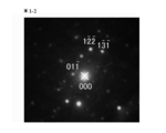
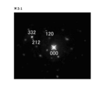
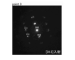
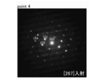
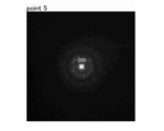
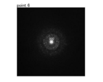
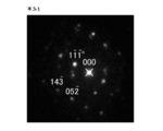
- 10B is a result of electron diffraction analysis of part (1-1) of FIG. 10A.
- 10B is a result of electron diffraction analysis of part (1-2) of FIG. 10A.
- 10B is a result of electron diffraction analysis of part (3-1) of FIG. 10A.
- 10B is a result of electron diffraction analysis of part (3-2) of FIG. 10A.
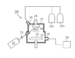
- FIG. 1 is an explanatory diagram of a first oxide film manufacturing apparatus in the present embodiment.
- 2A and 2B are explanatory diagrams showing one of the formation processes of the second oxide film in the present embodiment.
- the oxide sintered body that is the raw material for forming the oxide film is manufactured.
- copper oxide (Cu 2 O) which is an oxide of monovalent copper (Cu)
- Nb 2 O 5 which is an oxide of pentavalent niobium (Nb) were physically mixed.
- mixing was performed using a well-known Reika machine (manufactured by Ishikawa Factory, model AGA, hereinafter the same). Further, the above two kinds of oxides were mixed so that the stoichiometric ratio was 1 for Cu and 1 for Nb.
- the copper oxide of the present embodiment (Cu 2 O) is Kojundo Chemical Laboratory Co. nominal purity Corporation was employed those of 99.9%.
- the Nb 2 O 5 in the present embodiment Kojundo Chemical Laboratory Co. nominal purity Corporation was employed those of 99.9%.
- the above oxide mixture powder is compression-molded by using a commercially available tablet molding machine (NPTB Co., Ltd., model TB-5H), thereby forming the above oxide. Things were obtained. The pressure applied at this time was 35 MPa. Further, using this commercially available muffle furnace (model MS-2520, manufactured by Motoyama Co., Ltd.) heated to 950 ° C. with the compact placed on the above-mentioned powdery mixture placed on an alumina plate. A time firing step was performed.
- the relative density of the oxide sintered body obtained through the above firing step was about 90%.
- the crystal structure of this oxide sintered body is measured and analyzed using an X-ray diffraction (XRD) analyzer (manufactured by Rigaku Corporation, product name “automatic X-ray diffractometer RINT (registered trademark) 2400”). It was broken. As a result, it was found that the above-described oxide sintered body had a crystal structure of CuNbO 3 .
- the ⁇ / 2 ⁇ method was adopted.
- the voltage during X-ray irradiation was 40 kV and the tube current was 100 mA.
- the target of the X-ray generation part was copper.
- any of the following XRD analysis was performed using the above-mentioned XRD analyzer.
- an oxide film is manufactured on the substrate 10 using a pulse laser deposition apparatus 20.
- the laser source of the pulse laser deposition apparatus 20 was a model Compex 201 manufactured by Lambda Physik, and the chamber thereof was a pulse laser deposition apparatus manufactured by Neocera.
- the substrate 10 is a borosilicate glass substrate.
- the above oxide sintered body was adopted as the target 30.
- oxygen (O 2 ) and nitrogen (N 2 ) were supplied into the chamber 21 from the oxygen gas cylinder 25 a and the nitrogen gas cylinder 25 b through the inlet 26.
- the exhaust by the vacuum pump 29 was adjusted so that the equilibrium pressure of oxygen in the chamber 21 was 0.027 Pa.
- oxygen gas is introduced, but the present invention is not limited to this.
- nitrogen (N 2 ) gas instead of nitrogen (N 2 ) gas, an inert gas such as helium (He) gas or argon (Ar) gas may be introduced together with oxygen gas.
- oxygen gas may be introduced alone.
- the equilibrium pressure of oxygen in the chamber 21 of the present embodiment was 0.027 Pa, even if the pressure is set to other pressure (for example, 0.005 Pa to 100 Pa), the oxide film of the present embodiment Similar oxide films can be formed.
- a pulsed krypton fluoride (KrF) excimer laser (wavelength 248 nm) 22 is focused by the lens 23 and then irradiated toward the target 30 held by the holder 24.
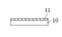
- the first oxide film 11 is formed on the substrate 10 by scattering the constituent atoms of the target 30 made of the above-described oxide sintered body by the above-described excimer laser irradiation.
- the composition ratio of the first oxide film 11 of this embodiment substantially matches that of the oxide sintered body that is the target 30. Therefore, the composition ratio is approximately 1 for Cu and 1 for Nb.
- the oscillation frequency of the excimer laser of this embodiment was 10 Hz, the energy per unit area of the unit pulse was 200 mJ per pulse, and the number of irradiations was 100,000.
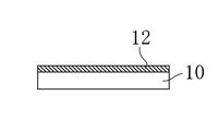
- the substrate 10 was taken out from the chamber 21 opened to the atmosphere. After removing indium adhering to the back surface of the substrate 10 with hydrochloric acid, a first oxidation on the substrate 10 is performed in a chamber in which an oxygen concentration is less than 1% by supplying nitrogen (N 2 ) gas. The physical film 11 was heat-treated (annealed) for 2 hours at 300 ° C. As a result, a second oxide film 12 was obtained on the substrate 10 as shown in FIG. 2B.
- the inventors measured the surfaces of the first oxide film 11 and the second oxide film 12 obtained in the present embodiment with an atomic force microscope (AFM) (model SSPI, manufactured by SII Nanotechnology, Inc.). -3700 / SPA-300 "). As a result, in the first oxide film 11, a pattern that seems to be particularly undulating or granular was not seen. On the other hand, with respect to the second oxide film 12, some patterns that seemed granular were visually recognized. Further, the thickness of the second oxide film 12 was measured using a laser microscope (manufactured by Keyence Corporation, product name “Color 3D Laser Microscope VK-850”), and as a result, the thickness was about 150 nm. Note that any of the following surface observations was performed using the aforementioned atomic force microscope. In addition, any of the following film thickness measurements were performed using the above-mentioned laser microscope and a scanning electron microscope (VE-9800) manufactured by Keyence Corporation.
- AFM atomic force microscope
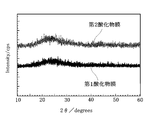
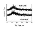
- the inventors analyzed the crystal states of the first oxide film 11 and the second oxide film 12 described above by XRD (X-ray diffraction).
- XRD X-ray diffraction
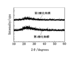
- the first oxide film 11 and the second oxide film 12 have peaks other than the wide halo peak considered to be derived from amorphous when 2 ⁇ is 20 ° to 30 °. It was not clearly observed. Therefore, based on the results of the above-mentioned XRD analysis, the first oxide film 11 and the second oxide film 12 of this embodiment are both aggregates of microcrystals, fine crystals that do not show clear diffraction peaks in the XRD analysis. It is considered to be amorphous including crystals, or amorphous.
- XRD analysis was also performed.
- the aggregate of microcrystals that do not show a clear diffraction peak in the XRD analysis the amorphous state including microcrystals, or any of 200 ° C, 400 ° C, and 500 ° C, or It is considered to be amorphous.
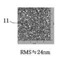
- the inventors analyzed the surface roughness of the first oxide film 11 and the second oxide film 12 with an atomic force microscope.
- the root mean square roughness (RMS) (hereinafter also simply referred to as “surface roughness”) of the surface of the first oxide film 11 in the present embodiment is about 24 nm.
- the surface roughness of the second oxide film 12 was found to be about 35 nm as shown in FIG.
- the inventors also analyze the surface roughness of the second oxide film when the first oxide film 11 is heat-treated at 200 ° C. and 500 ° C. for 2 hours. did.
- the inventors measured the electrical characteristics and conductivity of the first oxide film 11 and the second oxide film 12 described above by using a Hall effect measuring device (product name “Hall Effect Measurement System HMS-3000 Ver. Manufactured by ECOPIA). 3.5 ").
- the first oxide film 11 of the present embodiment has p-type conductivity, and its conductivity is about 0.011 S / cm.
- the second oxide film 12 of the present embodiment has p-type conductivity, and its conductivity is about 21.2 S / cm. Therefore, it has been found that the conductivity of the second oxide film 12 can be improved to about 2000 times that of the first oxide film 11 by the heat treatment described above.
- the conductivity of the second oxide film 12 is an extremely high numerical value as no other example of p-type conductivity.
- the band gap of the second oxide film 12 was found to be about 2.6 eV. Therefore, it was revealed that the second oxide film 12 of this embodiment has a relatively wide forbidden band width.
- the inventors also analyzed the electrical characteristics and conductivity of the second oxide film when the first oxide film 11 was heat-treated at 200 ° C. for 2 hours. went. As a result, the second oxide film had p-type conductivity and its conductivity was about 0.68 S / cm. Even with this value, it can be said that the conductivity is considerably higher than that of the prior art.
- the heat treatment of the first oxide film 11 in the range of 200 ° C. or higher and lower than 400 ° C. contributes to a dramatic improvement in conductivity as a p-type. It became.
- the heat treatment of the first oxide film 11 in the range of 200 ° C. or higher and 300 ° C. or lower is preferable from the above viewpoint.
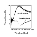
- visible light transmittance (hereinafter, simply referred to as “visible light transmittance” or “transmittance”) of the first oxide film 11 and the second oxide film 12 as described above for multichannel spectroscopy.
- the analysis was performed using an instrument (manufactured by Hamamatsu Photonics Co., Ltd., product name “multichannel spectrometer PMA-12”).
- a CCD linear image sensor “C1027-02” having a sensitivity wavelength range of 300 nm to 1100 nm was used.
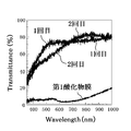
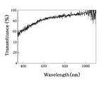
- FIG. 6 is a chart showing the analysis result of the transmittance of light having a wavelength mainly in the visible light region of the first oxide film 11 and the second oxide film 12 in the present embodiment.
- the transmittance of light having a wavelength of 400 nm or more and 800 nm or less of the first oxide film 11 is 40% or less, but for the second oxide film 12, the transmittance in that range jumps dramatically.
- the transmittance of light having a wavelength of about 470 nm or more and 1000 nm or less was found to be 60% or more.
- the transmittance was 70% or more.
- the 1 oxide film 11 in order to obtain an oxide film having high transmittance while maintaining high flatness, p-type conductivity and high conductivity, It is preferable to heat-process the 1 oxide film 11 at 200 degreeC or more and less than 400 degreeC. In addition, it is more preferable to heat-treat the first oxide film 11 particularly in the range of 200 ° C. or higher and 300 ° C. or lower.
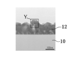
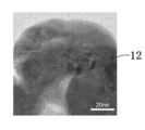
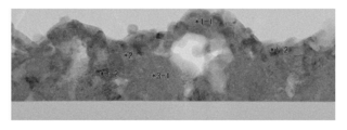
- FIG. 7A is a photograph observing the widest area among the three analysis results regarding the second oxide film 12. Further, FIG. 7B shows an enlarged photograph of a part (X part) of FIG. 7A and FIG. 7C shows a part of FIG. 7B (Y part).
- TEM field emission transmission electron microscope
- FIGS. 7A to 7C it was observed that the second oxide film 12 of the present embodiment was mainly composed of an aggregate of granular microcrystals having a major axis of 200 nm or less.
- the second oxide film 12 of the present embodiment is an amorphous state including an aggregate of microcrystals or microcrystals. Further, this TEM analysis also confirmed that the thickness of the second oxide film 12 was about 150 nm. Furthermore, according to the energy dispersive X-ray fluorescence (EDX) analyzer (VANTage (TM) manufactured by NORAN Instruments), which was performed together with the analysis by the TEM, the copper (Cu) and niobium of the second oxide film 12 were used. Although the atomic ratio of (Nb) is locally different, it was confirmed that the atomic ratio was approximately 1: 1 as a whole.
- EDX energy dispersive X-ray fluorescence
- the analysis conditions by the above TEM are as follows. First, for a sample to be analyzed, a carbon film is formed using a known high vacuum deposition apparatus in order to protect the outermost surface of the sample, and further a tungsten film is formed in a focused ion beam (FIB) processing apparatus. Been formed. And after the measurement area
- FIB focused ion beam
- the quantification method was a standardless method
- the correction method was an MBTS (Metalological biological thin section) method.
- the background Fit method was a Filter-Fit method.
- the acceleration voltage was 200 kV and the beam diameter was about 1 nm.
- the counting time was 30 seconds per point.
- the inventors produced the first oxide film and the second oxide film using the oxide sintered body having a low relative density (for example, 50%) by the same method as described above. As a result, it was found that the surface roughness of all of them increased. Therefore, it can be seen that a film having a rough surface is obtained by using an oxide sintered body having a low relative density.
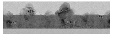
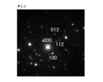
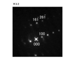
- FIG. 8A is a TEM photograph of the first oxide film 11
- FIGS. 8B to 8F are the results of electron beam diffraction analysis of specific locations in FIG. 8A, respectively.
- FIG. 8B shows the result of the location “1-1” in FIG. 8A
- FIG. 8C shows the result of the location “1-2” in FIG. 8A
- FIG. 8D is a result of the location “2” in FIG. 8A.
- FIG. 8E shows the result of the location “3-1” in FIG. 8A
- FIG. 8F shows the result of the location “3-2” in FIG. 8A.
- the first oxide film 11 includes not only microcrystals of a composite oxide (Cu X Nb Y O Z ) of at least niobium (Nb) and copper (Cu) but also niobium oxide (Nb X O Y). It was confirmed that the film also contains microcrystals.
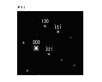
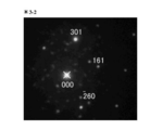
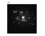
- FIG. 9A is a TEM photograph of the second oxide film 12 formed by heat-treating the first oxide film 11 at 300 ° C.
- FIGS. 9B to 9G show electron beam diffraction at specific locations in FIG. 9A, respectively. It is an analysis result. Specifically, FIG. 9B shows the result of the location “1” in FIG. 9A, FIG. 9C shows the result of the location “2” in FIG. 9A, and FIG. 9D shows the result of “3” in FIG. 9A. This is the result of the location. 9E shows the result of the location “4” in FIG. 9A, FIG.
- FIG. 9F shows the result of the location “5” in FIG. 9A
- FIG. 9G shows the result of the location “6” in FIG. 9A. It is.
- the crystal structure of Cu 2 O was confirmed in the locations of FIGS. 9B to 9D.
- the crystal structure of NbO 2 was confirmed at the locations in FIGS. 9E to G.
- the second oxide film 12 was a film containing at least microcrystals of niobium oxide (Nb X O Y ) and copper oxide (Cu X O Y ).
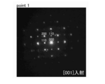
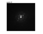
- FIG. 10A is a TEM photograph of the second oxide film 12 formed by heat-treating the first oxide film 11 at 500 ° C.
- FIGS. 10B to 10F respectively show the electrons at specific locations in FIG. 10A. It is a line diffraction analysis result.
- FIG. 10B shows the result of the location “1-1” in FIG. 10A
- FIG. 10C shows the result of the location “1-2” in FIG. 10A
- FIG. 10D shows the result of the location “2” in FIG. 10A
- FIG. 10E shows the result of the location “3-1” in FIG. 10A
- FIG. 10F shows the result of the location “3-2” in FIG. 10A.
- the second oxide film 12 includes not only microcrystals of a composite oxide (Cu X Nb Y O Z ) of at least niobium (Nb) and copper (Cu) but also niobium oxide (Nb X O Y). It was confirmed that the film also contains microcrystals.
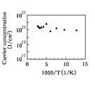
- FIG. 11A is a graph showing changes in resistivity with respect to temperature changes
- FIG. 11B is a graph showing changes in carrier density with respect to temperature changes.
- the resistivity and the carrier density hardly changed with respect to the temperature change. Therefore, it was found that the second oxide film 12 behaved like a degenerate semiconductor in electrical characteristics.
- the first oxide is the same as in the first embodiment except that the temperature of the stage 27 is 20 ° C. to 25 ° C. (so-called room temperature).
- a film 11 and a second oxide film 12 were formed. Therefore, the description which overlaps with 1st Embodiment may be abbreviate
- the surface roughness of the first oxide film 11 in this embodiment is about 1 nm
- the surface roughness of the second oxide film 12 is 1.7 nm to 2.3 nm or less.
- the second oxide film 12 of this embodiment is also considered to be an aggregate of microcrystals, an amorphous state including microcrystals, or an amorphous state.
- the temperature of the stage 27 (the set temperature) when the first oxide film 11 is manufactured. ) Is particularly preferably 0 ° C. or higher and 100 ° C. or lower.
- the first oxide film 11 in this embodiment has n-type conductivity, and its conductivity is about 0.061 S / cm.
- the second oxide film 12 had p-type conductivity, and the conductivity was about 4.22 S / cm.
- the visible light transmittance of the first oxide film 11 in this embodiment having a wavelength of 500 nm or more and 800 nm or less was about 40% or less.
- the visible light transmittance of a wavelength of about 580 nm or more and 1000 nm or less of the second oxide film 12 in this embodiment was 60% or more.
- the first oxide film 11 formed in the first embodiment was also heat-treated under the same conditions as in the first embodiment except that the first oxide film 11 was heated in an atmosphere in which oxygen was present at 1% or more. It was investigated. As a result, as shown in FIG. 12, the visible light transmittance of the oxide film after the heat treatment under the condition of the modification (1) of the first embodiment is the second oxide in the first embodiment. Compared to the transmittance of the film 12 with a wavelength of 500 nm or more and 1000 nm or less, it was found that the film 12 was considerably reduced except for some regions.
- the first oxide film 11 formed in the first embodiment was heat-treated in the atmosphere at 500 ° C.
- the oxide film after the heat treatment is referred to as a third oxide film. Except for the above-described conditions, the process is the same as that of the first embodiment. Therefore, the description which overlaps with 1st Embodiment may be abbreviate
- the third oxide film of this embodiment is considered to be a thin film containing divalent copper (Cu). Therefore, it is considered that by heating in the atmosphere, monovalent copper (Cu) is oxidized by oxygen in the air, so that it becomes divalent copper (Cu).
- the third oxide film is considered to be an aggregate of microcrystals that do not show a clear diffraction peak in the XRD analysis, an amorphous state including microcrystals, or an amorphous state.
- an oxide sintered body is manufactured through a compression molding process and a firing process by a tablet molding machine.
- the relative density of the oxide sintered body of the present embodiment is about 86%.
- XRD analysis of the oxide sintered body it was found that the oxide sintered body had a crystal structure of CuNb 3 O 8 .
- a first oxide film was manufactured on the substrate 10 using the pulse laser deposition apparatus 20 shown in FIG.
- an oxide sintered body having the above-described CuNb 3 O 8 crystal structure was adopted as the target 30.
- the temperature of the heater (not shown) inside the stage 27 is set to 20 ° C. to 25 ° C. (so-called room temperature).
- oxygen (O 2 ) was supplied into the chamber 21
- the exhaust by the vacuum pump 29 was adjusted so that the equilibrium pressure of oxygen in the chamber 21 was 0.027 Pa.
- the first oxide film 11 is formed on the substrate 10 by the pulsed krypton fluoride (KrF) excimer laser (wavelength 248 nm) 22 as shown in FIG. 2A. .
- the substrate is provided in a chamber in which an oxygen concentration is less than 1% by supplying nitrogen (N 2 ) gas.
- the first oxide film 11 on 10 was heat-treated (annealed) for 2 hours at 300 ° C.
- a second oxide film 12 was obtained on the substrate 10 as shown in FIG. 2B.
- the inventors observed the surfaces of the first oxide film 11 and the second oxide film 12 obtained in this embodiment with an atomic force microscope. As a result, the first oxide film 11 was a very flat film. On the other hand, with respect to the second oxide film 12, some patterns that seemed granular were visually recognized. Moreover, as a result of measuring the film thickness of the 2nd oxide film 12 using the said laser microscope, the film thickness was about 350 nm.
- the inventors analyzed the crystal states of the first oxide film 11 and the second oxide film 12 described above by XRD (X-ray diffraction).
- XRD X-ray diffraction
- the inventors analyzed the electrical characteristics and conductivity of the first oxide film 11 and the second oxide film 12 described above, and as a result, the first oxide film 11 of the present embodiment has p-type conductivity. And having an electrical conductivity of about 0.286 S / cm.
- the second oxide film 12 of the present embodiment has p-type conductivity, but its conductivity was about 0.0006 S / cm. Therefore, in the case of this embodiment, the phenomenon that electroconductivity falls by the above-mentioned heat processing was confirmed.
- the inventors analyzed the visible light transmittance of the first oxide film 11 and the second oxide film 12 described above. As a result, also in this embodiment, it was confirmed that the transmittance is improved by the above-described heat treatment.
- ⁇ Modification (2) of the second embodiment> Among the conditions of the pulse laser deposition apparatus 20 in the first or second embodiment, the point that the equilibrium pressure of oxygen in the chamber 21 is 0.0027 Pa, and the oxide sintered body in the second embodiment is the target 30. Other than the stoichiometric ratio of copper (Cu) and niobium (Nb) in the inside, the same conditions as in the first embodiment except for the results described later (1.11 (third time in Table 1)) A first oxide film 11 and a second oxide film 12 were formed. Therefore, the description which overlaps with 1st Embodiment may be abbreviate
- the inventors have formed a second oxide formed by heat-treating the first oxide film 11 formed using the target 30 in which the ratio of niobium (Nb) to copper (Cu) is changed under several temperature conditions.
- the film 12 was measured for electrical and optical properties.
- Table 1 shows the measurement results.
- FIG. 14 is a case where the target 30 in which the number of atoms of niobium (Nb) is 1.11 when the number of atoms of copper (Cu) is 1 among the results shown in Table 1, It is a chart which shows the analysis result of the transmittance
- the charts of the ratio of niobium (Nb) to copper (Cu) in Table 1 are 1.11 (first time) and 1.11 (second time) are “first time” and “2” in the chart of FIG. The second time is displayed.
- FIG. 14 also shows a chart of the transmittance of the first oxide film 11 before the heat treatment. Further, only for 1.11 (third time), in addition to the above differences, the number of times of excimer laser irradiation in the first embodiment was set to 50,000 times.
- the raw material for example, Cu 2 is produced at a certain ratio when the oxide sintered body that is the raw material for forming the oxide film that is the final target product is manufactured.
- O and Nb 2 O 5 are mixed, but it can be seen that the ratio is not limited to those of those embodiments, as shown in Table 1 and FIG. That is, for the second oxide film formed by heat-treating the first oxide film 11 at 300 ° C., when the number of copper (Cu) atoms is 1, the number of niobium (Nb) atoms is 1 or 1. In the case of 0.1, it can be seen that both the transmittance and the p-type conductivity are remarkably increased.
- the ratio of the raw materials in the above oxide sintered body when the number of copper (Cu) atoms is 1, the number of niobium (Nb) atoms is 0.00. If it is 25 or more and 4 or less, the oxide film provided with the characteristic according to the characteristic shown in the above-mentioned at least 1 part of Table 1 can be manufactured. This finding also applies to the atomic ratio of tantalum (Ta) to copper (Cu). Similarly, according to the inventors' additional investigation, from the viewpoint of enhancing electrical characteristics, the preferred range of the stoichiometric ratio of copper (Cu) and niobium (Nb) in the target 30 is copper (Cu).
- the number of niobium (Nb) atoms is 0.66 or more and 1.5 or less. Further, from the viewpoint of increasing the transmittance and electrical characteristics, a more preferable range described above is that when the number of copper (Cu) atoms is 1, the number of niobium (Nb) atoms is 0.66 or more and 1.25 or less. It is. Further, the above-described range that is more preferable from the above-described two viewpoints is that the number of niobium (Nb) atoms is 0.66 or more and 1.11 or less when the number of copper (Cu) atoms is 1. In addition, the most preferable range is that when the number of copper (Cu) atoms is 1, the number of niobium (Nb) atoms is 1 or more and 1.11 or less.
- the oxide sintered body that is the raw material for forming the oxide film is manufactured prior to the manufacture of the oxide film that is the final object.
- copper oxide (Cu 2 O) which is an oxide of monovalent copper (Cu)
- (Ta 2 O 5 ) which is an oxide of pentavalent tantalum (Ta) were physically mixed.
- mixing was performed using the above-described lykai machine. Further, the above-described two kinds of oxides were mixed so that the stoichiometric ratio was 1 for Cu and 1 for Ta. The rest is the same as each process of the first embodiment. Therefore, the description which overlaps with 1st Embodiment may be abbreviate
- the copper oxide of the present embodiment is Kojundo Chemical Laboratory Co. nominal purity Corporation was employed those of 99.9%.
- Ta 2 O 5 which has a present embodiment, Kojundo Chemical Laboratory Co. nominal purity Corporation was employed those of 99.9%.
- an oxide sintered body is manufactured through a compression molding process and a firing process by a tablet molding machine.
- the relative density of the oxide sintered body of the present embodiment is about 88%.
- a first oxide film is manufactured on the substrate 10 using the pulse laser deposition apparatus 20 shown in FIG.
- an oxide sintered body having the above-described crystal structure of CuTaO 3 was employed as the target 30.
- the temperature of the heater (not shown) inside the stage 27 is set to 20 ° C. to 25 ° C. (so-called room temperature).
- oxygen (O 2 ) was supplied into the chamber 21
- the exhaust by the vacuum pump 29 was adjusted so that the equilibrium pressure of oxygen in the chamber 21 was 0.13 Pa.
- the first oxide film 11 is formed on the substrate 10 by the pulsed krypton fluoride (KrF) excimer laser (wavelength 248 nm) 22 as shown in FIG. 2A. .
- nitrogen (N 2 ) gas is supplied to the substrate 10 on the substrate 10 in an atmosphere having an oxygen concentration of less than 1%.
- the first oxide film 11 was heat-treated (annealed) for 2 hours at 300 ° C.
- a second oxide film 12 was obtained on the substrate 10 as shown in FIG. 2B.
- the inventors observed the surfaces of the first oxide film 11 and the second oxide film 12 obtained in this embodiment with an atomic force microscope. As a result, the first oxide film 11 was a very flat film. On the other hand, with respect to the second oxide film 12, some patterns that seemed granular were visually recognized. Moreover, as a result of measuring the film thickness of the second oxide film 12 using a laser microscope, the film thickness was about 280 nm.
- the inventors analyzed the crystal states of the first oxide film 11 and the second oxide film 12 described above by XRD (X-ray diffraction).
- XRD X-ray diffraction
- the first oxide film 11 and the second oxide film 12 of this embodiment are both aggregates of microcrystals, fine crystals that do not show clear diffraction peaks in the XRD analysis. It is considered to be amorphous including crystals, or amorphous.
- the inventors analyzed the electrical characteristics and conductivity of the first oxide film 11 and the second oxide film 12 described above, and as a result, the first oxide film 11 of the present embodiment has p-type conductivity. And having an electrical conductivity of about 2.40 S / cm.
- the second oxide film 12 of the present embodiment has p-type conductivity, its conductivity was about 0.0086 S / cm. Therefore, in the case of this embodiment, the phenomenon that electroconductivity falls by the above-mentioned heat processing was confirmed.
- the inventors analyzed the visible light transmittance of the first oxide film 11 and the second oxide film 12 described above. As a result, the transmittance of light having a wavelength of 400 nm or more and 800 nm or less of the first oxide film 11 is 30% or less, but the transmittance in the range of the second oxide film 12 was improved.
- the transmittance of light having a wavelength of at least 500 nm to 800 nm is improved to 60% or more. did.
- the transmittance of light having a wavelength of about 550 nm to 800 nm was 70% or more. Therefore, also in this embodiment, it was confirmed that the transmittance is improved by the above-described heat treatment.
- copper oxide which is a monovalent copper oxide, and pentavalent tantalum, as a starting material of an oxide sintered body for forming the first oxide film 11 of the third embodiment, are used.
- the oxide was mixed so that the stoichiometric ratio of Cu was 1 and Ta was approximately 3. The rest is the same as each process of the first embodiment. Therefore, the description which overlaps with 1st Embodiment may be abbreviate
- an oxide sintered body is manufactured through a compression molding process and a firing process by a tablet molding machine.
- the relative density of the oxide sintered body of the present embodiment is about 55%.
- the oxide sintered body is considered to be a mixed crystal of an unknown complex oxide and Ta 2 O 5 at this stage.
- a first oxide film is manufactured on the substrate 10 using the pulse laser deposition apparatus 20 shown in FIG. Further, a CuTa 3 O 8 oxide sintered body having the above crystal structure was adopted as the target 30.
- the temperature of the heater (not shown) inside the stage 27 is set to 20 ° C. to 25 ° C. (so-called room temperature).
- the exhaust by the vacuum pump 29 was adjusted so that the equilibrium pressure of oxygen in the chamber 21 was 0.13 Pa.
- the first oxide film 11 is formed on the substrate 10 by the pulsed krypton fluoride (KrF) excimer laser (wavelength 248 nm) 22 as shown in FIG. 2A. .
- the first oxide film 11 was a flat film.
- nitrogen (N 2 ) gas is supplied to the substrate 10 on the substrate 10 in an atmosphere having an oxygen concentration of less than 1%.
- the first oxide film 11 was heat-treated (annealed) for 2 hours at 300 ° C.
- a second oxide film 12 was obtained on the substrate 10 as shown in FIG. 2B.
- the film thickness of the second oxide film 12 was about 190 nm.
- the inventors analyzed the crystal states of the first oxide film 11 and the second oxide film 12 described above by XRD (X-ray diffraction).
- XRD X-ray diffraction
- the first oxide film 11 and the second oxide film 12 of this embodiment are both aggregates of microcrystals and microcrystals that do not show clear diffraction peaks in the XRD analysis. It is considered to be amorphous or amorphous.
- the inventors analyzed the visible light transmittance of the first oxide film 11 and the second oxide film 12 described above. As a result, also in this embodiment, it was confirmed that the transmittance is improved by the above-described heat treatment.
- the first oxide film 11 is manufactured using the pulse laser deposition apparatus 20, but the manufacturing method of the first oxide film 11 is not limited to this.
- a physical vapor deposition method represented by an RF sputtering method or a magnetron sputtering method can be applied.
- the first oxide film 11 was formed using a high-frequency sputtering apparatus (RF sputtering apparatus) (manufactured by Eiko Engineering Co., Ltd.) having a known structure. At this time, the high frequency power was set to 90 W.
- the sputtering gas for the target 30 was a mixed gas in which argon (Ar) was mixed at a ratio of 5 to 95 (oxygen (O 2 )), and the pressure during film formation was 5.0 Pa.
- the substrate on which the first oxide film 11 was formed was a borosilicate glass substrate, and the temperature of the stage on which the substrate was placed was room temperature (20 ° C. to 25 ° C.).
- the surface temperature of the substrate rises (probably considered to be 100 ° C. or lower) during the film forming process by the sputtering method.
- the distance from the target to the substrate was 150 mm.
- the target used in this embodiment was the same target 30 as in the first embodiment except that the number of niobium (Nb) atoms was 1 when the number of copper (Cu) atoms was 3. . Under these conditions, a film forming process for 60 minutes was performed.
- FIG. 17 is a chart showing an analysis result of the transmittance of light having a wavelength mainly in the visible light region of the first oxide film 11 obtained by the above-described RF sputtering method.
- the transmittance of the first oxide film 11 is 80% or more in the visible light region having a wavelength of about 600 nm or more. Even in the region where the wavelength was about 400 nm to 600 nm, a high value of 60% or more was obtained.
- the first oxide film 11 is p-type and has a conductivity of 0.106 S / cm.
- the resistivity was 94.3 ⁇ cm, it was also revealed that the first oxide film was a film having a relatively low resistance.
- the carrier concentration of the first oxide film 11 was 1.91 ⁇ 10 17 (1 / cm 3 ), and the mobility was 0.348 (cm 3 / Vs).
- the inventors analyzed the crystalline state of the first oxide film 11 described above by XRD (X-ray diffraction). As a result, as shown in FIG. 18, in the first oxide film 11, any peak other than the broad halo peak considered to be derived from amorphous was not observed when 2 ⁇ was 20 ° to 30 °.
- the number of copper (Cu) atoms is 1.
- the number of atoms of niobium (Nb) was 1, it is not limited to that value.
- the atomic ratio of niobium (Nb) to copper (Cu) contained in the second oxide film 12 is 1 when the number of copper (Cu) atoms is 1, the number of niobium (Nb) atoms is 0. If it is 5 or more and 4 or less, the same effect as the first embodiment can be obtained.
- the second oxide film in this atomic ratio range has a high visible light transmittance with a wavelength of 500 nm to 800 nm (for example, 60% or more).
- the second oxide film in the above-mentioned atomic ratio range is considered to be an aggregate of microcrystals that do not show a clear diffraction peak in XRD analysis, an amorphous state including microcrystals, or an amorphous state. The presence of microcrystals has been confirmed by electron diffraction analysis. Therefore, it is interesting that the state of the second oxide film at least apparently differs depending on the measurement method.
- the oxide sintered compact is manufactured from the oxide as the target 30 for manufacturing the 1st oxide film 11 or the 2nd oxide film 12
- hydroxide for example, the oxide sintered body may be manufactured from copper hydroxide), nitrate (for example, copper nitrate), carbonate, or oxalate.
- the present invention can be widely used as an oxide film having p-type conductivity or a transparent conductive film having p-type conductivity.
Abstract
Description
11 第1酸化物膜
12 第2酸化物膜
20 パルスレーザー蒸着装置
21 チャンバー
22 エキシマレーザー
23 レンズ
24 ホルダー
25a 酸素ガスボンベ
25b 窒素ガスボンベ
26 導入口
27 ステージ
28 排気口
29 真空ポンプ
30 ターゲット
本実施形態では、銅(Cu)及びニオブ(Nb)とからなる酸化物膜及びその製造方法について説明する。図1は、本実施形態における第1酸化物膜の製造装置の説明図である。図2A及び図2Bは、本実施形態における第2酸化物膜の形成過程の1つを示す説明図である。
第1の実施形態におけるパルスレーザー蒸着装置20の条件のうち、ステージ27の温度が20℃乃至25℃(所謂、室温)である点以外は、第1の実施形態と同じ条件で第1酸化物膜11及び第2酸化物膜12が形成された。従って、第1の実施形態と重複する説明は省略され得る。
また、比較例として、第1の実施形態において形成された第1酸化物膜11が、500℃の大気中で加熱処理された。便宜上、この加熱処理後の酸化物膜を第3酸化物膜という。なお、前述の条件以外は、第1の実施形態の各プロセスと同様である。従って、第1の実施形態と重複する説明は省略され得る。
本実施形態では、第1の実施形態の第1酸化物膜11を形成するための酸化物焼結体の出発材としての、1価の銅の酸化物である酸化銅と5価のニオブの酸化物とが、化学量論比においてCuが1に対して、Nbがほぼ3となるように混合された。それ以外は、第1の実施形態の各プロセスと同様である。従って、第1の実施形態と重複する説明は省略され得る。
第1又は第2の実施形態におけるパルスレーザー蒸着装置20の条件のうち、チャンバー21内の酸素の平衡圧力が0.0027Paである点、及び第2の実施形態における酸化物焼結体がターゲット30中の銅(Cu)とニオブ(Nb)の化学量論比以外は、後述する一部(表1中の1.11(3回目))の結果を除いて第1の実施形態と同じ条件で第1酸化物膜11及び第2酸化物膜12が形成された。従って、第1の実施形態と重複する説明は省略され得る。

本実施形態では、最終目的物となる酸化物膜の製造に先立ち、その酸化物膜を形成するための原料となる酸化物焼結体の製造が行われた。まず、1価の銅(Cu)の酸化物である酸化銅(Cu2O)と、5価のタンタル(Ta)の酸化物である(Ta2O5)とが物理的に混合された。本実施形態では、上述のライカイ機を用いて混合された。また、上述の2種類の酸化物は、化学量論比においてCuが1に対して、Taがほぼ1となるように混合された。それ以外は、第1の実施形態の各プロセスと同様である。従って、第1の実施形態と重複する説明は省略され得る。なお、本実施形態の酸化銅(Cu2O)については、株式会社高純度化学研究所社製の公称純度が99.9%のものが採用された。また、本実施形態のTa2O5については、株式会社高純度化学研究所社製の公称純度が99.9%のものが採用された。
本実施形態では、第3の実施形態の第1酸化物膜11を形成するための酸化物焼結体の出発材としての、1価の銅の酸化物である酸化銅と5価のタンタルの酸化物とが、化学量論比においてCuが1に対して、Taがほぼ3となるように混合された。それ以外は、第1の実施形態の各プロセスと同様である。従って、第1の実施形態と重複する説明は省略され得る。
公知の構造を備える高周波スパッタリング装置(RFスパッタリング装置)(エイコーエンジニアリング社製)を用いて第1酸化物膜11が形成された。このとき、高周波電力が90Wに設定された。また、ターゲット30に対するスパッタリングガスは、アルゴン(Ar)が95に対して酸素(O2)が5の割合で混合された混合ガスであり、成膜中の圧力は5.0Paであった。また、第1酸化物膜11が形成された基板はホウケイ酸ガラス基板であり、その基板が載置されたステージの温度は室温(20℃~25℃)であった。但し、スパッタリング法による成膜工程中に、特に基板の表面温度が上昇(おそらく、100℃以下と考えられる)してしまうことは避けられない。また、ターゲットから基板までの距離は、150mmであった。なお、この実施形態で用いられたターゲットは、銅(Cu)の原子数を3とした場合にニオブ(Nb)の原子数が1となる以外は第1の実施形態と同じターゲッ30であった。これらの条件下において、60分間の成膜処理が行われた。
Claims (17)
- ニオブ(Nb)及びタンタル(Ta)からなる群から選択される1種類の遷移元素と、銅(Cu)とを含む酸化物の膜(不可避不純物を含み得る)であって、微結晶の集合体、微結晶を含むアモルファス状、又はアモルファス状であるとともに、p型の導電性を有する、
酸化物膜。 - 前記銅(Cu)に対する前記遷移元素の原子数比が、前記銅(Cu)の原子数を1とした場合に前記遷移元素の原子数が0.5以上3未満である、
請求項1に記載の酸化物膜。 - 前記酸化物膜が、微結晶の集合体又は微結晶を含むアモルファス状であって、1S/cm以上の導電率を有する、
請求項1又は請求項2に記載の酸化物膜。 - 400nm以上800nm以下の波長の光線の透過率が、40%以上である、
請求項1又は請求項2に記載の酸化物膜。 - 表面の二乗平均平方根粗さ(RMS)が1nm以上50nm以下である、
請求項1又は請求項2に記載の酸化物膜。 - 前記銅(Cu)の価数が1である、
請求項1又は請求項2に記載の酸化物膜。 - ニオブ(Nb)及びタンタル(Ta)からなる群から選択される1種類の遷移元素と、銅(Cu)とからなる酸化物(不可避不純物を含み得る)のターゲットの構成原子を飛散させることにより、基板上に微結晶の集合体、微結晶を含むアモルファス状、又はアモルファス状であってp型の導電性を有する第1酸化物膜(不可避不純物を含み得る)を形成する工程を含む、
酸化物膜の製造方法。 - 前記銅(Cu)に対する前記遷移元素の原子数比が、前記銅(Cu)の原子数を1とした場合に前記遷移元素の原子数が0.5以上3未満となる、
請求項7に記載の酸化物膜の製造方法。 - 前記第1酸化物膜を、酸素濃度が1%未満の環境下において200℃以上500℃以下で加熱することにより第2酸化物膜を形成する工程をさらに含む、
請求項7又は請求項8に記載の酸化物膜の製造方法。 - 前記第1酸化物膜を、酸素濃度が1%未満の環境下において200℃以上400℃未満で加熱することにより第2酸化物膜を形成する工程をさらに含む、
請求項7又は請求項8に記載の酸化物膜の製造方法。 - 第1酸化物膜を形成するときの前記基板の温度が0℃以上500℃以下である、
請求項7又は請求項8に記載の酸化物膜の製造方法。 - 前記ターゲットの構成原子を、スパッタリング又はパルスレーザーの照射により飛散させることによって前記第1酸化物膜を形成する、
請求項7又は請求項8に記載の酸化物膜の製造方法。 - ニオブ(Nb)及びタンタル(Ta)からなる群から選択される1種類の遷移元素と銅(Cu)とからなる酸化物(不可避不純物を含み得る)であって、
前記銅(Cu)に対する前記遷移元素の原子数比が、前記銅(Cu)の原子数を1とした場合に前記遷移元素の原子数が0.25以上4以下である、
ターゲット。 - 前記銅(Cu)に対する前記遷移元素の原子数比が、前記銅(Cu)の原子数を1とした場合に前記遷移元素の原子数が0.66以上1.5以下である、
請求項13に記載のターゲット。 - 前記ターゲットが、焼結されたものであって、相対密度が55%以上である、
請求項13又は請求項14に記載のターゲット。 - ニオブ(Nb)及びタンタル(Ta)からなる群から選択される1種類の遷移元素の酸化物(不可避不純物を含み得る)と銅(Cu)の酸化物(不可避不純物を含み得る)とを、前記銅(Cu)に対する前記遷移元素の原子数比が、前記銅(Cu)の原子数を1とした場合に前記遷移元素の原子数が0.25以上4以下となる割合で混合することにより混合物を得る混合工程と、
前記混合物を圧縮成形することにより成形体を得る成形工程と、
前記成形体を加熱することによって焼結させる焼結工程とを含む、
酸化物焼結体の製造方法。 - 前記銅(Cu)に対する前記遷移元素の原子数比が、前記銅(Cu)の原子数を1とした場合に前記遷移元素の原子数が0.66以上1.5以下である、
請求項16に記載の酸化物焼結体の製造方法。
Priority Applications (2)
| Application Number | Priority Date | Filing Date | Title |
|---|---|---|---|
| US13/576,567 US20120301673A1 (en) | 2010-02-01 | 2010-12-28 | Oxide film, process for producing same, target, and process for producing sintered oxide |
| CN201080062959.8A CN102741448B (zh) | 2010-02-01 | 2010-12-28 | 氧化物膜及其制造方法、与靶及氧化物烧结体的制造方法 |
Applications Claiming Priority (4)
| Application Number | Priority Date | Filing Date | Title |
|---|---|---|---|
| JP2010-020343 | 2010-02-01 | ||
| JP2010020343 | 2010-02-01 | ||
| JP2010170331A JP5641402B2 (ja) | 2010-02-01 | 2010-07-29 | 酸化物膜及びその製造方法、並びにターゲット及び酸化物焼結体の製造方法 |
| JP2010-170331 | 2010-07-29 |
Publications (1)
| Publication Number | Publication Date |
|---|---|
| WO2011092993A1 true WO2011092993A1 (ja) | 2011-08-04 |
Family
ID=44318992
Family Applications (1)
| Application Number | Title | Priority Date | Filing Date |
|---|---|---|---|
| PCT/JP2010/073700 WO2011092993A1 (ja) | 2010-02-01 | 2010-12-28 | 酸化物膜及びその製造方法、並びにターゲット及び酸化物焼結体の製造方法 |
Country Status (5)
| Country | Link |
|---|---|
| US (1) | US20120301673A1 (ja) |
| JP (1) | JP5641402B2 (ja) |
| KR (1) | KR20120112716A (ja) |
| CN (1) | CN102741448B (ja) |
| WO (1) | WO2011092993A1 (ja) |
Cited By (1)
| Publication number | Priority date | Publication date | Assignee | Title |
|---|---|---|---|---|
| JP2013199682A (ja) * | 2012-03-26 | 2013-10-03 | Ryukoku Univ | 酸化物膜及びその製造方法 |
Families Citing this family (5)
| Publication number | Priority date | Publication date | Assignee | Title |
|---|---|---|---|---|
| CN105358734B (zh) * | 2014-05-08 | 2017-03-29 | 三井金属矿业株式会社 | 溅镀靶材 |
| JP6503928B2 (ja) * | 2015-06-29 | 2019-04-24 | コニカミノルタ株式会社 | 電子写真感光体、画像形成装置および画像形成方法 |
| WO2018092598A1 (ja) * | 2016-11-17 | 2018-05-24 | 日本化学工業株式会社 | 亜酸化銅粒子、その製造方法、光焼結型組成物、それを用いた導電膜の形成方法及び亜酸化銅粒子ペースト |
| JP7172902B2 (ja) * | 2019-07-29 | 2022-11-16 | トヨタ自動車株式会社 | 酸素吸蔵材 |
| CN111678927A (zh) * | 2020-06-08 | 2020-09-18 | 首钢集团有限公司 | 一种钢铁表面氧化物的分析方法 |
Citations (1)
| Publication number | Priority date | Publication date | Assignee | Title |
|---|---|---|---|---|
| JP2009246085A (ja) * | 2008-03-31 | 2009-10-22 | Hitachi Ltd | 半導体装置およびその製造方法 |
Family Cites Families (5)
| Publication number | Priority date | Publication date | Assignee | Title |
|---|---|---|---|---|
| KR100300919B1 (ko) * | 1996-11-15 | 2001-10-29 | 하루타 히로시 | 열전소자의제조방법 |
| JP4446064B2 (ja) * | 2004-07-07 | 2010-04-07 | 独立行政法人産業技術総合研究所 | 熱電変換素子及び熱電変換モジュール |
| US7657377B2 (en) * | 2007-05-31 | 2010-02-02 | Cbg Corporation | Azimuthal measurement-while-drilling (MWD) tool |
| JP2009047969A (ja) * | 2007-08-21 | 2009-03-05 | Seiko Epson Corp | プロジェクタおよび表示装置 |
| JP2010031346A (ja) * | 2008-07-02 | 2010-02-12 | Central Glass Co Ltd | 酸化亜鉛薄膜及び薄膜積層体 |
-
2010
- 2010-07-29 JP JP2010170331A patent/JP5641402B2/ja not_active Expired - Fee Related
- 2010-12-28 WO PCT/JP2010/073700 patent/WO2011092993A1/ja active Application Filing
- 2010-12-28 CN CN201080062959.8A patent/CN102741448B/zh not_active Expired - Fee Related
- 2010-12-28 KR KR1020127020398A patent/KR20120112716A/ko not_active Application Discontinuation
- 2010-12-28 US US13/576,567 patent/US20120301673A1/en not_active Abandoned
Patent Citations (1)
| Publication number | Priority date | Publication date | Assignee | Title |
|---|---|---|---|---|
| JP2009246085A (ja) * | 2008-03-31 | 2009-10-22 | Hitachi Ltd | 半導体装置およびその製造方法 |
Non-Patent Citations (1)
| Title |
|---|
| HEINRICH, ANDREAS ET AL.: "Influence of oxygen pressure, temperature and substrate/target distance on CU2Ta4012 thin films prepared by pulsed-laser deposition", THIN SOLID FILMS, vol. 479, 7 December 2004 (2004-12-07), pages 12 - 16 * |
Cited By (2)
| Publication number | Priority date | Publication date | Assignee | Title |
|---|---|---|---|---|
| JP2013199682A (ja) * | 2012-03-26 | 2013-10-03 | Ryukoku Univ | 酸化物膜及びその製造方法 |
| CN104204279A (zh) * | 2012-03-26 | 2014-12-10 | 学校法人龙谷大学 | 氧化物膜及其制造方法 |
Also Published As
| Publication number | Publication date |
|---|---|
| JP5641402B2 (ja) | 2014-12-17 |
| CN102741448B (zh) | 2014-04-09 |
| KR20120112716A (ko) | 2012-10-11 |
| US20120301673A1 (en) | 2012-11-29 |
| JP2011174167A (ja) | 2011-09-08 |
| CN102741448A (zh) | 2012-10-17 |
Similar Documents
| Publication | Publication Date | Title |
|---|---|---|
| TWI460144B (zh) | Oxide sintered body and sputtering target | |
| Li et al. | Defect-mediated phase transition temperature of VO 2 (M) nanoparticles with excellent thermochromic performance and low threshold voltage | |
| JP5641402B2 (ja) | 酸化物膜及びその製造方法、並びにターゲット及び酸化物焼結体の製造方法 | |
| JP5764828B2 (ja) | 酸化物焼結体およびそれを加工したタブレット | |
| JP2011184715A (ja) | 酸化亜鉛系透明導電膜形成材料、その製造方法、それを用いたターゲット、および酸化亜鉛系透明導電膜の形成方法 | |
| EP3101153B1 (en) | Cu-ga alloy sputtering target and method for producing same | |
| JP6237221B2 (ja) | 非晶質酸化物およびそのエレクトライドの薄膜の製造方法 | |
| JP6277977B2 (ja) | 酸化物焼結体、スパッタリング用ターゲット、及びそれを用いて得られる酸化物半導体薄膜 | |
| JP2007246318A (ja) | 酸化物焼結体、その製造方法、酸化物透明導電膜の製造方法、および酸化物透明導電膜 | |
| JP5392633B2 (ja) | ZnO系透明導電膜用ターゲットおよびその製造方法 | |
| JP5582530B2 (ja) | 紫外線領域透過型透明導電膜及びその製造方法 | |
| JP5167575B2 (ja) | 酸化物焼結体、スパッタリングターゲットおよび透明導電膜 | |
| JP5952031B2 (ja) | 酸化物焼結体の製造方法およびターゲットの製造方法 | |
| JP5494082B2 (ja) | 導電性酸化物とその製造方法 | |
| JP4136531B2 (ja) | 透明導電膜、及びその製造方法 | |
| KR20180117631A (ko) | 산화물 소결체 및 스퍼터링용 타겟 | |
| JP5996227B2 (ja) | 酸化物膜及びその製造方法 | |
| JP2017193755A (ja) | 透明導電膜の製造方法、及び透明導電膜 | |
| Su et al. | Microstructural characterization and field emission properties of tungsten oxide and titanium-oxide-doped tungsten oxide nanowires | |
| JP5526904B2 (ja) | 導電性酸化物焼結体とその製造方法 | |
| Ramasamy et al. | Recent study of nanomaterials prepared by inert gas condensation using ultra high vacuum chamber | |
| WO2022202640A1 (ja) | 透明導電膜、透明導電膜の製造方法、透明導電部材、電子ディスプレイ機器、および太陽電池 | |
| WO2014021374A1 (ja) | 酸化物焼結体およびそれを加工したタブレット | |
| JP2001307553A (ja) | 透明導電膜およびその製造方法並びにその用途 | |
| CN113661143A (zh) | 薄膜的制造方法以及层叠体 |
Legal Events
| Date | Code | Title | Description |
|---|---|---|---|
| WWE | Wipo information: entry into national phase |
Ref document number: 201080062959.8 Country of ref document: CN |
|
| DPE2 | Request for preliminary examination filed before expiration of 19th month from priority date (pct application filed from 20040101) | ||
| 121 | Ep: the epo has been informed by wipo that ep was designated in this application |
Ref document number: 10844747 Country of ref document: EP Kind code of ref document: A1 |
|
| NENP | Non-entry into the national phase |
Ref country code: DE |
|
| WWE | Wipo information: entry into national phase |
Ref document number: 13576567 Country of ref document: US |
|
| ENP | Entry into the national phase |
Ref document number: 20127020398 Country of ref document: KR Kind code of ref document: A |
|
| 122 | Ep: pct application non-entry in european phase |
Ref document number: 10844747 Country of ref document: EP Kind code of ref document: A1 |