WO2011092864A1 - Dispositif de transmission de signaux - Google Patents
Dispositif de transmission de signaux Download PDFInfo
- Publication number
- WO2011092864A1 WO2011092864A1 PCT/JP2010/051354 JP2010051354W WO2011092864A1 WO 2011092864 A1 WO2011092864 A1 WO 2011092864A1 JP 2010051354 W JP2010051354 W JP 2010051354W WO 2011092864 A1 WO2011092864 A1 WO 2011092864A1
- Authority
- WO
- WIPO (PCT)
- Prior art keywords
- switch
- transistor
- coil
- pulse signal
- signal
- Prior art date
Links
Images


Classifications
-
- H—ELECTRICITY
- H04—ELECTRIC COMMUNICATION TECHNIQUE
- H04L—TRANSMISSION OF DIGITAL INFORMATION, e.g. TELEGRAPHIC COMMUNICATION
- H04L25/00—Baseband systems
- H04L25/02—Details ; arrangements for supplying electrical power along data transmission lines
- H04L25/0264—Arrangements for coupling to transmission lines
- H04L25/0272—Arrangements for coupling to multiple lines, e.g. for differential transmission
- H04L25/0276—Arrangements for coupling common mode signals
Definitions
- the present application relates to a signal transmission device that transmits a signal input to a transmission circuit to a reception circuit that is electrically insulated from the transmission circuit.
- a technique for driving a non-optical isolator that transmits and receives a signal through a separation barrier such as a transformer with an H bridge is known.
- An example of a conventional signal transmission device 100 is shown in FIG.
- the signal input to the input terminal IN is transmitted to the receiving circuit 130.
- the ground potential GNDL on the transmission side and the ground potential GNDH on the reception side are separated.
- An H bridge is formed by the transistors P1, P2, N1, and N2.
- the transformer TR includes a transmission coil L1 and a reception coil L2.
- the H-bridge transistors P1, P2, N1, and N2 are on / off controlled in accordance with a signal input to the input terminal IN.
- the receiving circuit 130 detects a signal input to the input terminal from the current flowing through the receiving coil L2.
- the series resistance components of the transmission coil L1 are Rs1 and Rs2
- the series resistance components of the reception coil L2 are Rs3 and Rs4.
- Cc1 and Cc2 be parasitic capacitances between the transmission coil L1 and the reception coil L2.
- the capacitance value of each of the parasitic capacitances Cc1 and Cc2 is a capacitance C
- the resistance value of each of the series resistance components Rs3 and Rs4 is a resistance R.
- the path i1 is a path from one end of the receiving coil L2 to the ground ground potential GNDL via the parasitic capacitance Cc1, the series resistance component Rs1, and the transistor N1.
- the path i1 is an asymmetric current path for the transformer TR.
- the displacement current i flows through the path i2 when the transistor N2 is on.
- the path i2 is a path from the other end of the receiving coil L2 to the ground potential GNDL via the parasitic capacitance Cc2, the series resistance component Rs2, and the transistor N2.
- the path i2 is also an asymmetric current path for the transformer TR.
- the signal transmission device disclosed in the present application is a device that includes a transmission coil and a reception coil, the transmission coil and the reception coil are electrically insulated, and transmits a signal from the transmission coil to the reception coil.
- the signal transmission device includes an upper first switch connected between a first end of the transmission coil and a supply terminal for a high reference potential, and a first transfer switch between the first end of the transmission coil and a supply terminal for a low reference potential.
- a lower first switch connected is provided.
- the signal transmission device includes an upper second switch connected between the second end of the transmission coil and the supply terminal for the high reference potential, and a second transfer switch between the second end of the transmission coil and the supply terminal for the low reference potential.
- a lower second switch to be connected is provided.
- the signal transmission device further includes a switch control unit that controls each of the upper first switch, the lower first switch, the upper second switch, and the lower second switch.
- the switch control unit turns on the upper first switch and the lower second switch and turns off the upper second switch and the lower first switch, thereby generating a coil current in the first direction in the transmission coil, and then The first control for turning on the lower first switch is performed in response to turning off the upper first switch. Further, the switch control unit turns off the upper first switch and the lower second switch and turns on the upper second switch and the lower first switch, thereby causing the transmitting coil to generate a coil current in the second direction. Then, the second control is performed to turn on the lower second switch in response to turning off the upper second switch.
- the transmission coil and the reception coil are electrically insulated, and the lower reference potential of the transmission coil and the lower reference potential of the reception coil are separated.
- a transformer is formed by the transmission coil and the reception coil.
- a parasitic capacitance exists between the transmission coil and the reception coil.
- a common mode voltage is applied between the lower reference potential supply terminal of the transmission coil and the lower reference potential supply terminal of the reception coil, a displacement current flows through the parasitic capacitance.
- the displacement current is transferred from the reception coil to the lower reference of the transmission circuit via the parasitic capacitance and the transmission coil. Flows to potential. Since a series resistance component exists at both ends of the receiving coil, when a displacement current flows through the receiving coil, a noise voltage is generated by the series resistance component.
- the lower first switch is turned on in response to the upper first switch being turned off during the first control. Further, the lower second switch is turned on in response to the upper second switch being turned off during the second control. Then, there is a period in which both the lower first switch and the lower second switch are on. In this period, the potentials of both the first end and the second end of the transmission coil are set to the low reference potential, and the low impedance state is set. Since both the first end and the second end are in a low impedance state, the displacement current due to the common mode voltage is generated from the first current path (from one end of the receiving coil to the parasitic capacitance, the first of the transmitting coil).
- the switch control unit detects the rising edge of the input signal and outputs the first pulse signal, and detects the falling edge of the input signal.
- a second pulse output unit for outputting the second pulse signal, a first inversion unit for generating an inverted first pulse signal obtained by inverting the first pulse signal, and an inverted second pulse obtained by inverting the second pulse signal.
- a second inversion unit for generating a signal.
- the first pulse signal is supplied to the upper first switch
- the inverted first pulse signal is supplied to the lower first switch
- the second pulse signal is supplied to the upper second switch, so that the inverted second pulse is supplied.
- the signal may be supplied to the lower second switch.
- the first pulse signal is supplied to the upper first switch, and the inverted first pulse signal is supplied to the lower first switch.
- the first pulse signal and the inverted first pulse signal are complementary signals. Therefore, in the first control, it is possible to perform control to turn on the lower first switch in response to turning off the upper first switch.
- the second pulse signal is supplied to the upper second switch, and the inverted second pulse signal is supplied to the lower second switch.
- the second pulse signal and the inverted second pulse signal are complementary signals. Therefore, in the second control, it is possible to perform control to turn on the lower second switch in response to turning off the upper second switch. This makes it possible to perform switch control so that there is a period in which both the lower first switch and the lower second switch are on.
- the switch control unit further includes a delay circuit that delays rising edges of the first pulse signal, the second pulse signal, the inverted first pulse signal, and the inverted second pulse signal for a predetermined time. Can do.
- the first pulse signal and the second pulse signal output from the delay circuit are supplied to the upper first switch and the upper second switch, and the inverted first pulse signal and the inverted second pulse signal output from the delay circuit are It may be supplied to the first side switch and the second lower switch.
- the delay circuit When the rising edge of the inverted first pulse signal is delayed by the delay circuit, the first pulse signal and the inverted first pulse signal are both between the falling edge of the first pulse signal and the rising edge of the inverted first pulse signal. A dead time period that is low level occurs. In the dead time period, since both the upper first switch and the lower first switch are turned off, it is possible to prevent a through current from flowing from the upper first switch to the lower first switch. Similarly, the delay circuit can generate a dead time period between the falling edge of the second pulse signal and the rising edge of the inverted second pulse signal. Therefore, it is possible to prevent a through current from flowing from the upper second switch to the lower second switch.
- the signal transmission device disclosed in the present application further includes a lower first current path connected in parallel with the lower first switch, and a lower second current path connected in parallel with the lower second switch. be able to. Further, the impedance of the lower first current path is set higher than the impedance when the lower first switch is turned on, and the impedance of the lower second current path is equal to the impedance when the lower second switch is turned on. It may be higher than that.
- the lower first current path always connects the first end of the transmission coil to the supply terminal for the lower reference potential.
- the lower second current path always connects the second end of the transmission coil to the supply terminal for the lower reference potential. Therefore, both the first end portion and the second end portion of the transmission coil can always be maintained in the low impedance state even during the period in which the lower first switch and the lower second switch are turned off. Thereby, it can suppress that the noise voltage by a common mode voltage generate
- the impedance of the lower first current path is set higher than the impedance when the lower first switch is turned on, and the impedance of the lower second current path is equal to the impedance when the lower second switch is turned on. It is higher than that. Therefore, the value of the through current flowing from the upper first switch to the lower first current path and the value of the through current flowing from the upper second switch to the lower second current path can be sufficiently reduced.
- each of the lower first switch, the lower second switch, the lower first current path, and the lower second current path may include an NMOS transistor.
- the size of the NMOS transistor in the lower first current path may be smaller than the size of the NMOS transistor in the lower first switch.
- the size of the NMOS transistor in the lower second current path may be smaller than the size of the NMOS transistor in the lower second switch.
- the switch control unit may control the NMOS transistors of the lower first current path and the lower second current path to be always on.
- the lower first current path and the lower second current path can be formed by the transistor. Therefore, it is not necessary to create a separate high-impedance current path, and the circuit design and manufacturing process can be simplified. Further, the impedance when the NMOS transistor of the lower first current path is on is higher than the impedance when the NMOS transistor of the lower first switch is on. The impedance of the lower second current path when the NMOS transistor is on is higher than the impedance when the NMOS transistor of the lower second switch is on. Therefore, the value of the through current flowing from the upper first switch to the lower first current path and the value of the through current flowing from the upper second switch to the lower second current path can be sufficiently reduced.
- the signal transmission device disclosed in the present application may include an NMOS transistor in each of the lower first switch, the lower second switch, the lower first current path, and the lower second current path.
- the lower first current path may further include a first resistor connected to the drain terminal of the NMOS transistor.
- the lower second current path may further include a second resistor connected to the drain terminal of the NMOS transistor.
- the switch control unit may control the NMOS transistors of the lower first current path and the lower second current path to be always on.
- the impedance when these transistors are on can be increased. Therefore, the value of the through current flowing from the upper first switch to the lower first current path and the value of the through current flowing from the upper second switch to the lower second current path can be sufficiently reduced.
- the signal transmission device disclosed in the present application may further include a parallel first switch connected in parallel to the upper first switch and a parallel second switch connected in parallel to the upper second switch.
- the switch control unit may perform control to simultaneously turn on the upper first switch and the parallel first switch, and then turn off the upper first switch and the parallel first switch at different timings.
- the switch control unit may perform control to simultaneously turn on the upper second switch and the parallel second switch and then turn off the upper second switch and the parallel second switch at different timings.
- the reception coil voltage is proportional to the time change rate (di / dt) of the current flowing through the transmission coil.
- the upper first switch and the parallel first switch are controlled to be turned on at the same time when turned on and turned off at different timings when turned off.
- the upper second switch and the parallel second switch are controlled to be turned on simultaneously when turned on and turned off at different timings when turned off. Then, the time change rate of the current flowing through the transmission coil can be controlled so that the decrease rate at the off time becomes smaller than the increase rate at the on time.
- the amplitude value of the pulse voltage generated in the receiving coil in response to the switch being turned on can be made larger than the amplitude value of the pulse voltage generated in the receiving coil in response to the switch being turned off. Therefore, it is possible to easily detect when the switch is turned on in the receiving coil.
- the signal transmission device of the present application does not need to perform control of gently turning off the switch, and therefore does not need to use an intermediate potential of the on / off voltage of the switch. Thereby, since the control of the time change rate of the current flowing through the transmission coil can be realized in a stable state, the generation of noise can be suppressed.
- each of the upper first switch, the parallel first switch, the upper second switch, and the parallel second switch may include a PMOS transistor.
- the size of the PMOS transistor of the parallel first switch may be smaller than the size of the PMOS transistor of the upper first switch.
- the size of the PMOS transistor of the parallel second switch may be smaller than the size of the PMOS transistor of the upper second switch.
- the switch control unit may perform control to turn off the upper first switch after turning off the parallel first switch. Further, in the second control, after the parallel second switch is turned off, the upper second switch may be turned off.
- the transistor size of the upper first switch is larger than the transistor size of the parallel first switch. Then, the parallel first switch is turned off first, and the upper first switch is turned off later. Similarly, the size of the transistor of the upper second switch is larger than the size of the transistor of the parallel second switch. Then, the parallel second switch is turned off first, and the upper second switch is turned off later. Thereby, the time change rate of the current flowing through the transmission coil can be controlled so that the decrease rate at the off time becomes smaller than the increase rate at the on time.
- the number of turns of the reception coil may be larger than the number of turns of the transmission coil.
- the signal component is also deteriorated as the coupling coefficient is deteriorated, so that signal transmission becomes difficult. Therefore, in the signal transmission device of the present application, by increasing the number of turns of the receiving coil, the inductance of the receiving coil can be increased and the signal component can be increased. Therefore, the transformer can be reduced in size, and the cost of the signal transmission device can be reduced. Note that when the number of turns of the receiving coil is increased, the series resistance component is also increased, so that the noise voltage is also increased. However, in the signal transmission device of the present application, since the generation of the noise voltage itself can be suppressed, the number of turns of the receiving coil can be increased.
- FIG. 1 is a circuit diagram of a motor drive system according to Embodiment 1.
- FIG. 3 is a circuit diagram of a signal transmission circuit according to the first embodiment.
- FIG. 3 is a circuit diagram of a rising delay circuit according to the first embodiment.
- FIG. 3 is an operation waveform diagram of the rising delay circuit according to the first embodiment.
- FIG. 3 is a circuit diagram of a receiving circuit according to the first embodiment. It is an operation
- FIG. FIG. 6 is an operation waveform diagram according to a general operation method of the signal transmission circuit according to the first exemplary embodiment. 6 is a circuit diagram of a transmission circuit according to Embodiment 2.
- FIG. 1 is a circuit diagram of a motor drive system according to Embodiment 1.
- FIG. 3 is a circuit diagram of a signal transmission circuit according to the first embodiment.
- FIG. 3 is a circuit diagram of a rising delay circuit according to the first embodiment.
- FIG. 6 is a circuit diagram of a transmission circuit according to Embodiment 3.
- FIG. FIG. 6 is a circuit diagram of a falling delay circuit according to a third embodiment.
- FIG. 10 is an operation waveform diagram of the falling delay circuit according to the third embodiment.
- FIG. 10 is an operation waveform diagram of the transmission circuit according to the third embodiment. It is a figure which shows the modification of an H bridge circuit. It is a circuit diagram of the signal transmission apparatus of a prior art.
- FIG. 1 shows a motor drive system 50.
- the motor drive system 50 includes a low voltage system circuit 60 and a high voltage system circuit 70.
- the low voltage system circuit 60 and the high voltage system circuit 70 are insulated.
- the low voltage system circuit 60 includes a low voltage battery 61 and a microcomputer 62.
- the microcomputer 62 outputs a control signal CS.
- the control signal CS is a signal for controlling the switch operation of the switching circuit 72.
- the high voltage system circuit 70 includes a control circuit 71, a switching circuit 72, a motor 73, and a high voltage battery 74.
- the control circuit 71 includes a signal transmission circuit 1 and a drive circuit 75.
- the signal transmission circuit 1 is a circuit including an insulating signal device.
- the signal transmission circuit 1 transmits the control signal CS output from the microcomputer 62 to the drive circuit 75 while maintaining insulation.
- the control circuit 71 is formed as an integrated IC by using a small device such as an on-chip transformer as the insulated signal device. Therefore, size reduction and cost reduction are achieved.
- the drive circuit 75 drives the switching circuit 72 according to the control signal CS. Thereby, the rotation of the motor 73 is controlled.
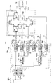
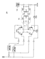
- FIG. 2 shows a detailed circuit diagram of the signal transmission circuit 1.
- the signal transmission circuit 1 includes an input terminal IN, a transmission circuit 10, a transformer TR, a reception circuit 30, and an output terminal OUT.
- the transmission circuit 10 and the reception circuit 30 are insulated by a transformer TR. Further, the ground potential GNDL of the transmission circuit 10 and the ground potential GNDH of the transformer TR are separated.
- An input voltage VIN is input to the input terminal IN, and an output voltage VOUT is output from the output terminal OUT.
- the transmission circuit 10 includes a switch control circuit 20, inverters 15 and 16, buffers 17 and 18, and an H bridge circuit 19.
- the switch control circuit 20 will be described.
- the switch control circuit 20 includes pulse generators 11 and 12, an inverter 13, and a delay control circuit 14.
- the pulse generator 11 receives the input voltage VIN and outputs a pulse signal PS1.
- the pulse generator 12 receives the input voltage VIN inverted by the inverter 13 and outputs a pulse signal PS2.
- the delay control circuit 14 includes rising delay circuits 21 to 24 and inverters 25 and 26.
- the rising delay circuit 21 receives the pulse signal PS2 and outputs the gate control signal SP2.
- the rising delay circuit 22 receives the pulse signal PS1 and outputs the gate control signal SP1.
- the inverter 25 receives the pulse signal PS1 and outputs the inverted pulse signal PS1B.
- the rising delay circuit 23 receives the inverted pulse signal PS1B and outputs the gate control signal SN1.
- the inverter 26 receives the pulse signal PS2 and outputs the inverted pulse signal PS2B.
- the rising delay circuit 24 receives the inverted pulse signal PS2B and outputs the gate control signal SN2.
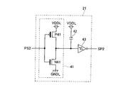
- FIG. 3 shows a block diagram of the rising delay circuit 21.
- the rising delay circuit 21 includes an inverter 41, a capacitor 42, and a Schmitt trigger inverter 43.
- the inverter 41 includes a transistor P41 which is a PMOS transistor and a transistor N41 which is an NMOS transistor.
- the gate terminal of the transistor P41 and the gate terminal of the transistor N41 are connected in common and serve as an input terminal.
- the power supply potential VDDL is input to the source terminal of the transistor P41.
- the ground potential GNDL is input to the source terminal of the transistor N41.
- the drain terminal of the transistor P41 and the drain terminal of the transistor N41 are commonly connected to serve as an output terminal.
- the size of the transistor P41 is larger than the size of the transistor N41. Therefore, the impedance when the transistor P41 is on is lower than the impedance when the transistor N41 is on.
- the pulse signal PS2 is input to the input terminal of the inverter 41.
- the output terminal of the inverter 41 and the input terminal of the Schmitt trigger inverter 43 are connected to the first end of the capacitor 42.
- the power supply potential VDDL is input to the second end of the capacitor 42.
- the Schmitt trigger inverter 43 outputs a gate control signal SP2.
- FIG. 4 shows an operation waveform diagram of the rising delay circuit 21.
- the pulse signal PS2 transits from low level to high level at time t41
- the output of the inverter 41 transits from high level to low level.
- the capacitor 42 is discharged by the current path of the capacitor 42, the transistor N41, and the ground potential GNDL.
- the gate control signal SP2 changes from low level to high level at time t42.
- the pulse signal PS2 transits from high level to low level at time t43
- the output of the inverter 41 transits from low level to high level.
- the capacitor 42 is charged by the current path of the power supply potential VDDL, the transistor P41, and the capacitor 42.
- the gate control signal SP2 transitions from the high level to the low level at time t43.
- the rising delay circuit 21 can perform an operation of outputting only the rising edge of the pulse signal PS2 by delaying by the delay time DT1 and outputting the falling edge without delaying.
- the length of the delay time DT1 can be set to an arbitrary value by adjusting the resistance value of the transistor N41 and the capacitance value of the capacitor 42.
- the configuration of the rising delay circuits 22 to 24 is the same as that of the rising delay circuit 21, and therefore detailed description thereof is omitted here.
- the H bridge circuit 19 (FIG. 2) includes transistors P1, P2, N1, and N2.
- Transistors P1 and P2 are PMOS transistors, and transistors N1 and N2 are NMOS transistors.
- the drain terminal of the transistor P1 is connected to the first input terminal T11 of the transformer TR.
- the power supply potential VDDL is input to the source terminal of the transistor P1.
- the gate control signal SP1 inverted by the inverter 16 is input to the gate terminal of the transistor P1.
- the transistor P1 is turned on when the gate control signal SP1 is at a high level, and is turned off when the gate control signal SP1 is at a low level.
- the drain terminal of the transistor N1 is connected to the first input terminal T11 of the transformer TR.
- the ground potential GNDL is input to the source terminal of the transistor N1.
- a gate control signal SN1 is input to the gate terminal of the transistor N1 through the buffer 17. The transistor N1 is turned on when the gate control signal SN1 is at a high level, and is turned off when the gate control signal SN1 is at a low level.
- the drain terminal of the transistor P2 is connected to the second input terminal T12 of the transformer TR.
- the power supply potential VDDL is input to the source terminal of the transistor P2.
- the gate control signal SP2 inverted by the inverter 15 is input to the gate terminal of the transistor P2.
- the transistor P2 is turned on when the gate control signal SP2 is at a high level, and is turned off when the gate control signal SP2 is at a low level.
- the drain terminal of the transistor N2 is connected to the second input terminal T12 of the transformer TR.
- the ground potential GNDL is input to the source terminal of the transistor N2.
- a gate control signal SN2 is input to the gate terminal of the transistor N2 through the buffer 18.
- the transistor N2 is turned on when the gate control signal SN2 is at a high level, and is turned off when the gate control signal SN2 is at a low level.
- the drain terminal of the transistor P1 and the drain terminal of the transistor N1 are connected at the node ND1. Similarly, the drain terminal of the transistor P2 and the drain terminal of the transistor N2 are connected at the node ND2.
- the transformer TR will be described.
- the transformer TR in FIG. 2 is an equivalent circuit.
- the transformer TR includes a transmission coil L1 and a reception coil L2.
- the transmission coil L1 and the reception coil L2 are electrically insulated. Further, the number of turns of the receiving coil L2 is set larger than the number of turns of the transmitting coil L1.
- a node ND1 is connected to the first input terminal T11 of the transformer TR, and a node ND2 is connected to the second input terminal T12.
- the receiving circuit 30 is connected to the first output terminal T21 of the transformer TR.
- the second output terminal T22 is supplied with the ground potential GNDH. Further, a current flowing through the transmission coil L1 is defined as a coil current I1, and a current flowing through the reception coil L2 is defined as a coil current I2.
- a series resistance component Rs1 exists in the connection path between the first end E11 of the transmission coil L1 and the first input terminal T11.
- a series resistance component Rs2 exists in the connection path between the second end E12 and the second input terminal T12.
- a series resistance component Rs3 exists in the connection path between the first end E21 of the receiving coil L2 and the first output terminal T21.
- a series resistance component Rs4 exists in the connection path between the second end E22 and the second output terminal T22.
- a parasitic capacitance Cc1 exists between the first end E11 of the transmission coil L1 and the first end E21 of the reception coil L2.
- a parasitic capacitance Cc2 exists between the second end E12 of the transmission coil L1 and the second end E22 of the reception coil L2.
- each capacitance value of the parasitic capacitances Cc1 and Cc2 is defined as a capacitance C.
- each resistance value of the series resistance components Rs3 and Rs4 is defined as a resistance R.
- FIG. 5 shows the receiving circuit 30.
- the receiving circuit 30 includes a low-pass filter 31, a high-pass filter 32, comparators cmp1 and cmp2, a signal processing circuit 33, and an RS flip-flop 34.
- the first output terminal T21 of the transformer TR is connected to the input terminal of the low-pass filter 31.
- the output terminal of the low pass filter 31 is connected to the input terminal of the high pass filter 32.
- the reception coil voltage Vd is output from the output terminal of the high pass filter 32.
- the receiving coil voltage Vd is input to the non-inverting input terminal of the comparator cmp1, the threshold Vthp is input to the inverting input terminal, and the output signal Vc1 is output from the output terminal. Further, the receiving coil voltage Vd is input to the non-inverting input terminal of the comparator cmp2, the threshold Vthn is input to the inverting input terminal, and the output signal Vc2 is output from the output terminal.
- the output signals Vc1 and Vc2 are input to the signal processing circuit 33, and the pulse signal Vs and the pulse signal Vr are output.
- the signal processing circuit 33 is a circuit that detects a rising edge and a falling edge of the input voltage VIN. Specifically, when the output signal Vc1 is continuously input to the signal processing circuit 33 and the output signal Vc2 is sequentially input in the subsequent order, the signal processing circuit 33 is in the positive direction (the same direction as the arrow of the coil current I1 in FIG. 2). It is determined that the coil current I1 is generated. Therefore, it is determined that the rising edge of the input voltage VIN is input to the transmission circuit 10, and the pulse signal Vs is output from the signal processing circuit 33.
- the coil current I1 in the negative direction (the direction opposite to the arrow of the coil current I1 in FIG. 2). Is determined to occur. Therefore, it is determined that the falling edge of the input voltage VIN is input to the transmission circuit 10, and the pulse signal Vr is output from the signal processing circuit 33.
- the pulse signal Vs is input to the set terminal of the RS flip-flop 34, and the pulse signal Vr is input to the reset terminal.
- the RS flip-flop 34 outputs a high level output voltage VOUT when the pulse signal Vs is input, and outputs a low level output voltage VOUT when the pulse signal Vr is input.
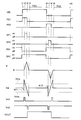
- the operation of the signal transmission circuit 1 will be described using the operation waveform diagram of FIG.
- the period PE1 is a period in which the input voltage VIN is at a high level
- the period PE2 is a period in which the input voltage VIN is at a low level.
- period PE1 Operation of period PE1 will be described.
- the pulse signal PS1 changes to high level in accordance with the rising edge of the input voltage VIN (arrow Y1).
- the gate control signal SN1 transitions to a low level (arrow Y2). Therefore, the transistor N1 is turned off at time t1.
- the gate control signal SP1 transitions to the high level after a delay time DT1 from the rising edge of the pulse signal PS1 (arrow Y3). Therefore, the transistor P1 is turned on at time t2.
- the transistor P2 is turned off and the transistor N2 is turned on.
- a current path of the power supply potential VDDL, the transistor P1, the node ND1, the transmission coil L1, the node ND2, the transistor N2, and the ground potential GNDL is formed, and the coil current I1 starts to increase in the positive direction. That is, a positive coil current I1 flows in accordance with the rising edge of the input voltage VIN.
- a secondary voltage proportional to the increase rate (di / dt) of the coil current I1 is generated by electromagnetic induction.
- the secondary voltage is input to the low-pass filter 31 and the high-pass filter 32, and noise is removed. From the high pass filter 32, the secondary voltage after noise removal is output as the reception coil voltage Vd. Then, during a period in which the reception coil voltage Vd exceeds the threshold value Vthp, the output signal Vc1 of the comparator cmp1 becomes high level (arrow Y4).
- the gate control signal SP1 transitions to a low level in accordance with the falling edge of the pulse signal PS1 (arrow Y5). Therefore, at time t3, the transistor P1 is turned off and the current path is interrupted, so that the coil current I1 starts to decrease. Further, the gate control signal SN1 transitions to the high level with a delay of the delay time DT1 from the falling edge of the pulse signal PS1 (arrow Y6). Therefore, the transistor N1 is turned on at time t4.
- the high-pass filter 32 outputs a reception coil voltage Vd that is proportional to the reduction rate (di / dt) of the coil current I1. Then, during the period when the reception coil voltage Vd is lower than the threshold value Vthn, the output signal Vc2 of the comparator cmp2 becomes low level (arrow Y7).
- the signal processing circuit 33 (FIG. 5) of the receiving circuit 30, it is detected that the pulse of the output signal Vc1 is input first and the pulse of the output signal Vc2 is sequentially input in the subsequent order. Therefore, in the signal processing circuit 33, it is determined that the rising edge of the input voltage VIN is input to the transmission circuit 10, and the output voltage VOUT is set to the high level (arrow Y8). As a result, the rising edge at time t1 of the input voltage VIN is restored as the output voltage VOUT, whereby signal transmission is performed.
- the delay control circuit 14 forms a dead time of the delay time DT1 between the falling edge of the gate control signal SN1 at time t1 and the rising edge of the gate control signal SP1 at time t2.
- the delay control circuit 14 forms a dead time of the delay time DT1 between the falling edge of the gate control signal SP1 at time t3 and the rising edge of the gate control signal SN1 at time t4.
- the dead time period since both the transistors P1 and N1 are turned off, it is possible to prevent a through current from flowing from the transistor P1 to the transistor N1.
- period PE2 the pulse signal PS2 changes to high level in accordance with the falling edge of the input voltage VIN (arrow Y11).
- the gate control signal SN2 transitions to a low level (arrow Y12). Therefore, the transistor N2 is turned off at time t6.
- the gate control signal SP2 transitions to a high level after a delay time DT1 from the rising edge of the pulse signal PS2 (arrow Y13). Therefore, the transistor P2 is turned on at time t7. At time t7, the transistor P1 is turned off and the transistor N1 is turned on.
- the high-pass filter 32 outputs a reception coil voltage Vd proportional to the rate of increase (di / dt) of the coil current I1. Then, during the period when the reception coil voltage Vd is lower than the threshold value Vthn, the output signal Vc2 of the comparator cmp2 becomes low level (arrow Y14).
- the gate control signal SP2 transitions to the low level according to the falling edge of the pulse signal PS2 (arrow Y15). Therefore, at time t8, the transistor P2 is turned off and the current path is interrupted, so that the coil current I1 starts to decrease. Further, the gate control signal SN2 transitions to the high level with a delay of the delay time DT1 from the falling edge of the pulse signal PS2 (arrow Y16). Therefore, the transistor N2 is turned on at time t9.
- the high-pass filter 32 outputs a reception coil voltage Vd that is proportional to the reduction rate (di / dt) of the coil current I1. Then, during a period in which the reception coil voltage Vd exceeds the threshold value Vthp, the output signal Vc1 of the comparator cmp1 becomes high level (arrow Y17).
- the signal processing circuit 33 determines that this is a case where the falling edge of the input voltage VIN is input to the transmission circuit 10, and the output voltage VOUT is set to the low level (arrow Y18). As a result, the falling edge of the input voltage VIN at time t6 is restored as the output voltage VOUT, whereby signal transmission is performed.
- a first effect in the signal transmission circuit 1 according to the first embodiment will be described.
- a case will be described in which a common mode voltage VCM is applied between a supply terminal for the ground potential GNDL on the transmission side and a supply terminal for the ground potential GNDH on the reception side.
- the voltage change rate of the common mode voltage VCM is (dv / dt) will be described.
- a case will be described in which the potential of the transmission-side ground potential GNDL is lower than the potential of the reception-side ground potential GNDH.
- FIG. 7 is a waveform diagram when the signal transmission circuit 1 is operated by a general method.
- the gate control signal SN1 in the period PE1, the gate control signal SN1 is maintained at a low level and the gate control signal SN2 is maintained at a high level, whereby the transistor N1 is maintained in an off state and the transistor N2 is maintained in an on state.
- the gate control signal SN1 is maintained at a high level and the gate control signal SN2 is maintained at a low level, whereby the transistor N1 is maintained in an on state and the transistor N2 is maintained in an off state. That is, in a general operation method, the transistors N1 and N2 are not simultaneously turned on (low impedance state).
- the path through which the displacement current i flows is the path Ri2 in FIG.
- the path Ri2 is a path from the second end E22 of the receiving coil L2 to the ground potential GNDL via the parasitic capacitance Cc2, the series resistance component Rs2, the second input terminal T12, the node ND2, and the transistor N2.
- the path Ri2 is an asymmetric path for the transformer TR.
- the path through which the displacement current i flows is the path Ri1 in FIG.
- the path Ri1 is a path from the first end E21 of the receiving coil L2 to the ground potential GNDL via the parasitic capacitance Cc1, the series resistance component Rs1, the first input terminal T11, the node ND1, and the transistor N1. Further, the path Ri1 is an asymmetric path for the transformer TR.
- the gate control signal is generated in the period from time t4 to time t6 (area A1) in period PE1 and in the period from time t9 to time t10 in period PE2 (area A2).
- time t4 to time t6 area A1
- time t9 to time t10 in period PE2
- both SN1 and SN2 are at a high level and both transistors N1 and N2 are on.
- the potentials of both the first end E11 and the second end E12 of the transmission coil L1 are in a low impedance state.
- the displacement current i due to the common mode voltage VCM flows through both the path Ri1 and the path Ri2. That is, in the signal transmission circuit 1 of the present application, unlike the general operation method of FIG. 7, the current path of the displacement current does not become one of the paths Ri2 and Ri1. Then, the current path of the displacement current i can be made symmetric for the transformer TR. Therefore, since displacement currents in opposite directions flow at both ends of the receiving coil L2, the influence of the displacement current can be offset. Therefore, it can suppress that noise voltage generate
- the second effect of the signal transmission circuit 1 according to the first embodiment will be described. If the transformer TR is downsized, the received signal component also deteriorates with the deterioration of the coupling coefficient, so that signal transmission becomes difficult. Therefore, in the signal transmission circuit 1 according to the first embodiment, by increasing the number of turns of the reception coil L2 as compared with the number of turns of the transmission coil L1, the inductance of the reception coil L2 can be increased and the strength of the reception signal can be increased. . Therefore, the transformer TR can be downsized, and the cost of the signal transmission circuit 1 can be reduced. Note that when the number of turns of the receiving coil L2 is increased, the series resistance components Rs3 and Rs4 are also increased, so that the noise voltage due to the common mode voltage VCM is also increased. However, in the signal transmission circuit 1 according to the first embodiment, since the generation of the noise voltage due to the common mode voltage VCM can be suppressed, the number of turns of the receiving coil L2 can be increased.
- FIG. 8 is a detailed circuit diagram of the transmission circuit 10a according to the second embodiment. Note that the configurations of the transformer TR and the receiving circuit 30 are the same as those in the first embodiment (FIG. 2), and thus detailed description thereof is omitted here.
- the transmission circuit 10a includes a switch control circuit 20a, inverters 15 and 16, buffers 17 and 18, and an H bridge circuit 19a.
- the switch control circuit 20a includes pulse generators 11 and 12, an inverter 13, and a delay control circuit 14a.
- the delay control circuit 14a outputs the power supply potential VDDL as the gate control signal SN3. Since the other configuration of the delay control circuit 14a is the same as that of the delay control circuit 14 (FIG. 2) of the first embodiment, detailed description thereof is omitted here.
- the H bridge circuit 19a includes transistors P1 and P2 and transistors N1 to N4.
- Transistors P1 and P2 are PMOS transistors, and transistors N1 to N4 are NMOS transistors.
- the H bridge circuit 19a has a configuration in which transistors N3 and N4 are added to the H bridge circuit 19 (FIG. 2) of the first embodiment.
- the transistor N3 is connected in parallel with the transistor N1.
- the drain terminal of the transistor N3 is connected to the node ND1.
- the ground potential GNDL is input to the source terminal of the transistor N3, and the gate control signal SN3 is input to the gate terminal.
- the transistor N3 is always turned on.
- Transistor N4 is connected in parallel with transistor N2.
- the drain terminal of the transistor N4 is connected to the node ND2.
- the ground potential GNDL is input to the source terminal of the transistor N4, and the gate control signal SN3 is input to the gate terminal.
- the transistor N4 is always turned on.
- the size of the transistor N3 is smaller than the size of the transistor N1. Therefore, the impedance when the transistor N3 is on is higher than the impedance when the transistor N1 is on. Thereby, the through current flowing from the transistor P1 to N3 can be reduced during the period in which the transistor P1 is turned on.
- the size of the transistor N4 is smaller than the size of the transistor N2. Therefore, the impedance when the transistor N4 is on is higher than the impedance when the transistor N2 is on. Thereby, the through current flowing from the transistor P2 to N4 can be reduced during the period in which the transistor P2 is turned on.
- the sizes of the transistors N3 and N4 are preferably about 1/10 to 1/50 of the size of the transistors N1 and N2. Since other configurations are the same as those of the H-bridge circuit 19 (FIG. 2) of the first embodiment, detailed description thereof is omitted here.
- the transistors N3 and N4 are always on. Therefore, both the first end E11 and the second end E12 of the transmission coil L1 can always be maintained in a low impedance state. Thereby, the displacement current i due to the common mode voltage VCM flows through both the paths Ri1a and Ri2a (FIG. 8). Then, since the current path of the displacement current i is symmetric for the transformer TR, it is possible to suppress the generation of a noise voltage on the receiving coil L2 side. Thereby, in the receiving circuit 30, generation
- the path Ri1a is formed by the transistor N3, and the path Ri2a is formed by the transistor N4.
- the paths Ri1a and Ri2a can be created using the same process as the process of creating the transistors N1 and N2. Therefore, it is not necessary to separately prepare a dedicated process for forming the paths Ri1a and Ri2a, and the circuit design and manufacturing process can be simplified.
- FIG. 9 shows a detailed circuit diagram of the transmission circuit 10b according to the third embodiment. Note that the configurations of the transformer TR and the receiving circuit 30 are the same as those in the first embodiment (FIG. 2), and thus detailed description thereof is omitted here.
- the transmission circuit 10b includes a switch control circuit 20b, inverters 15, 16, 57, 58, buffers 17, 18, 53 to 56, and an H bridge circuit 19b.
- the switch control circuit 20b includes pulse generators 11 and 12, an inverter 13, and a delay control circuit 14b.
- the delay control circuit 14b includes rising delay circuits 21 to 24, 27 and 28, 51 and 52, and inverters 25 and 26.
- the rising delay circuit 27 receives the pulse signal PS1 and outputs the gate control signal SP1b.
- the falling delay circuit 51 receives the pulse signal PS1 and outputs the delayed pulse signal PS1D.
- the rising delay circuit 22 receives the delayed pulse signal PS1D and outputs the gate control signal SP1.
- the inverter 25 receives the delayed pulse signal PS1D and outputs the inverted delayed pulse signal PS1DB.
- the rising delay circuit 23 receives the inverted delay pulse signal PS1DB and outputs the gate control signal SN1.
- the pulse signal PS2 is input to the rising delay circuit 28, and the gate control signal SP2b is output.
- the falling delay circuit 52 receives the pulse signal PS2 and outputs the delayed pulse signal PS2D.
- the rising delay circuit 21 receives the delayed pulse signal PS2D and outputs the gate control signal SP2.
- the inverter 26 receives the delayed pulse signal PS2D and outputs the inverted delayed pulse signal PS2DB.
- the rising delay circuit 24 receives the inverted delay pulse signal PS2DB and outputs the gate control signal SN2.
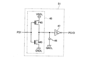
- FIG. 10 shows a block diagram of the falling delay circuit 51.
- the falling delay circuit 51 includes an inverter 45, a capacitor 46, and a Schmitt trigger inverter 47.
- the inverter 45 includes a transistor P45 that is a PMOS transistor and a transistor N45 that is an NMOS transistor.
- the size of the transistor N45 is larger than the size of the transistor P45. Therefore, the impedance when the transistor N45 is on is lower than the impedance when the transistor P45 is on.
- the pulse signal PS1 is input to the input terminal of the inverter 45.
- the output terminal of the inverter 45 and the input terminal of the Schmitt trigger inverter 47 are connected to the first end of the capacitor 46.
- the ground potential GNDL is input to the second end of the capacitor 42.
- the Schmitt trigger inverter 47 outputs a delay gate control signal PS1D.
- FIG. 11 shows an operation waveform diagram of the falling delay circuit 51.
- the capacitor 42 is discharged by the current path of the capacitor 46, the transistor N45, and the ground potential GNDL.
- the capacitor 46 is charged by the power supply potential VDDL, the current path of the transistor P45, and the capacitor 46.
- the falling delay circuit 51 can perform an operation of outputting only the falling edge of the pulse signal PS1 by delaying by the delay time DT2 and outputting the rising edge without delaying. Further, the length of the delay time DT2 can be set to an arbitrary value by adjusting the resistance value of the transistor P45 and the capacitance value of the capacitor 46. Since the configuration of the falling delay circuit 52 is the same as that of the falling delay circuit 51, detailed description thereof is omitted here. The other configuration of the delay control circuit 14b is the same as that of the delay control circuit 14 (FIG. 2) according to the first embodiment, and thus detailed description thereof is omitted here.
- the H bridge circuit 19b (FIG. 9) includes transistors P1, P2, P1b, P2b, N1, and N2.
- the transistors P1b and P2b are PMOS transistors.
- the H bridge circuit 19b has a configuration in which transistors P1b and P2b are added as compared with the H bridge circuit 19 (FIG. 2) of the first embodiment.
- the transistor P1b is connected in parallel with the transistor P1.
- the drain terminal of the transistor P1b is connected to the node ND1.
- the power supply potential VDDL is input to the source terminal of the transistor P1b.
- the gate control signal SP1b inverted by the inverter 57 is input via the buffer 53 to the gate terminal of the transistor P1b.
- the transistor P1b is turned on when the gate control signal SP1b is at a high level, and is turned off when the gate control signal SP1b is at a low level.
- the transistor P2b is connected in parallel with the transistor P2.
- the drain terminal of the transistor P2b is connected to the node ND2.
- the power supply potential VDDL is input to the source terminal of the transistor P2b.
- the gate control signal SP2b inverted by the inverter 58 is input to the gate terminal of the transistor P2b via the buffer 55.
- the size of the transistor P1b is smaller than the size of the transistor P1. Therefore, the impedance when the transistor P1b is on is higher than the impedance when the transistor P1 is on.
- the size of the transistor P2b is smaller than the size of the transistor P2. Therefore, the impedance when the transistor P2b is on is higher than the impedance when the transistor P2 is on.
- the other configuration of the H-bridge circuit 19b is the same as that of the H-bridge circuit 19 (FIG. 2) of the first embodiment, and thus detailed description thereof is omitted here.
- the operation of the transmission circuit 10b will be described using the operation waveform diagram of FIG.
- the period PE1 is a period in which the input voltage VIN is at a high level
- the period PE2 is a period in which the input voltage VIN is at a low level.
- a dead time corresponding to the delay time DT1 is formed by the rising delay circuits 21 to 24, 27, and 28 of the delay control circuit 14b.
- the mechanism for forming the dead time is the same as that described in the first embodiment. Therefore, in FIG. 12, for the sake of easy understanding, the description of the dead time is omitted.
- period PE1 Operation of period PE1 will be described.
- the pulse signal PS1 changes to high level in accordance with the rising edge of the input voltage VIN (arrow Y20).
- the gate control signals SP1 and SP1b simultaneously transition to a high level (arrow Y21). Therefore, the transistors P1 and P1b are turned on.
- the gate control signal SN1 transitions to a low level in response to the rising edge of the pulse signal PS1. Therefore, the transistor N1 is turned off. As a result, a first current path passing through the transistor P1 and a second current path passing through the transistor P1b are formed.
- the first current path is a path from the power supply potential VDDL to the ground potential GNDL via the transistor P1, the node ND1, the transformer TR, the node ND2, and the transistor N2.
- the second current path is a path from the power supply potential VDDL to the ground potential GNDL via the transistor P1b, the node ND1, the transformer TR, the node ND2, and the transistor N2. Then, the coil current I1 flows through both the first current path and the second current path. At this time, since the coil current I1 flows through the two paths, the combined impedance of the current path is set to a low state. Therefore, the increase rate (di / dt) of the coil current I1 is increased.
- the receiving coil voltage Vd is obtained in proportion to the increasing rate of the coil current I1 flowing in the transmitting coil L1 (arrow Y22).
- the waveform of the reception coil voltage Vd has a mountain shape protruding upward in the figure, and its amplitude is the amplitude AM1.
- the reception circuit 30 determines that the coil current I1 in the positive direction (the same direction as the arrow of the coil current I1 in FIG. 2) has occurred. . Thereby, it is detected that the rising edge of the input voltage VIN is input to the transmission circuit 10, and the output voltage VOUT is set to the high level (arrow Y23).
- the gate control signal SP1b changes to the low level in accordance with the falling edge of the pulse signal PS1 (arrow Y24). Therefore, since the transistor P1b is turned off and the second current path is interrupted, the current path of the coil current I1 is only one of the first current paths. Then, since the combined impedance of the current path is set to a high state, the coil current I1 starts to decrease.
- the gate control signal SP1 transitions to a low level with a delay of DT2 from the falling edge of the pulse signal PS1b. Therefore, the transistor P1 is turned off and the first current path is interrupted. Therefore, since both the first current path and the second current path are interrupted, the coil current I1 starts to decrease with a larger slope.
- the gate control signal SN1 transitions to a high level, so that the transistor N1 is turned on.
- the coil current I1 becomes zero.
- the reception coil voltage Vd is obtained in proportion to the reduction rate (di / dt) of the coil current I1 (arrow Y25).
- the waveform of the reception coil voltage Vd has a valley shape protruding downward in the figure, and its amplitude is the amplitude AM2.
- the decreasing slope of the coil current I1 from the time t22 to t24 is made smaller than the increasing slope of the coil current I1 from the time t21 to t22. Therefore, in the reception coil voltage Vd, the amplitude AM2 when the coil current I1 decreases is smaller than the amplitude AM1 when the coil current I1 increases.
- the size of the transistor P1 is larger than the size of the transistor P1b. Then, the transistor P1b is turned off first, and the transistor P1 is turned off later. Therefore, the reduction rate of the coil current I1 from time t22 to t23 can be controlled to be smaller than the reduction rate of the coil current I1 from time t23 to t24.
- the same operation as that in the period PE1 is performed. Therefore, the decreasing slope of the coil current I1 from the time t27 to t29 is made smaller than the increasing slope of the coil current I1 from the time t26 to t27. Therefore, in the reception coil voltage Vd, the amplitude AM2 when the coil current I1 decreases is smaller than the amplitude AM1 when the coil current I1 increases.
- the operation content of the period PE2 is the same as the operation content of the period PE1, and thus detailed description thereof is omitted here.
- the reception coil voltage Vd is proportional to the time change rate (di / dt) of the coil current I1 flowing through the transmission coil L1.
- the transistors P1 and P1b are controlled to be turned on at the same time when turned on (time t21) and turned off at different timings (time t22, t23) when turned off.
- the transistors P2 and P2a are controlled to be turned on at the same time when turned on (time t21) and turned off at different timings (time t22, t23) when turned off.
- the time change rate of the coil current I1 flowing through the transmission coil L1 can be controlled so that the decrease rate when the transistor is off is smaller than the increase rate when the transistor is on.
- the amplitude AM1 of the reception coil voltage Vd generated when the transistor is turned on can be made larger than the amplitude AM2 of the reception coil voltage Vd generated when the transistor is turned off. Therefore, the waveform appearing in the reception coil voltage Vd corresponding to the rising time of the input voltage VIN (time t21) can be a mountain shape (time t21 to t22) having a large amplitude.
- the waveform appearing in the reception coil voltage Vd corresponding to the falling time of the input voltage VIN can be a valley shape (time t26 to t27) having a large amplitude. Then, the rising edge of the input voltage VIN can be detected by detecting that the reception coil voltage Vd exceeds the threshold value Vthp by the comparator cmp1 having the threshold value Vthp. Further, when the comparator cmp2 having the threshold value Vth detects that the reception coil voltage Vd is lower than the threshold value Vthn, the falling time of the input voltage VIN can be detected. Therefore, the receiving coil L2 can easily detect when the transistor is on. As a result, the output voltage VOUT can be restored more reliably.
- the transmission circuit 10b of the present application does not need to perform control of gently turning off the transistor, and therefore does not need to use an intermediate potential of the on / off voltage of the transistor.
- the H-bridge circuit 19a includes a transistor N3 connected in parallel with the transistor N1 and a transistor N4 connected in parallel with the transistor N2.
- the transistors N3 and N4 are controlled to be always on.
- resistors R3 and R4 may be added to the drain terminals of the transistors N3 and N4.
- the impedance when the transistors N3 and N4 are turned on can be increased. Therefore, the value of the through current flowing from the transistor P1 to the transistor N3 and the value of the through current flowing from the transistor P2 to the transistor N4 can be sufficiently reduced.
- the impedances when the transistors N3 and N4 are turned on can be adjusted by the resistors R3 and R4. Therefore, it is not necessary to adjust the impedance when the transistor is turned on by adjusting the size of the transistor. Thereby, the sizes of the transistors N3 and N4 can be arbitrarily set.
- the present invention is not limited to this configuration.
- the transistor N3 may not be provided, and the node ND1 may be connected to the ground potential GNDL only by the resistor R3.
- the transistor N4 may not be provided, and the node ND1 may be connected to the ground potential GNDL only by the resistor R4. This also allows both the first end E11 and the second end E12 of the transmission coil L1 to be always kept in a low impedance state.
- the transistors N1 and N2 are turned on during the period from time t4 to time t6 in the period PE1 (area A1) and during the period from time t9 to time t10 in the period PE2 (area A2).
- control for turning on both of the transistors P1 and P2 may be performed. This also achieves the purpose of making the potential across the transmission coil L1 low impedance.
- the transistors N1 and N2 can be reliably operated even when the power supply potential VDDL is not stable, such as when the signal transmission circuit 1 starts up or falls, and thus stable operation of the H bridge circuit 19 is expected. it can.
- the present invention is not limited to this mode.
- the potential at both ends of the transmission coil L1 may always be maintained at the power supply potential VDDL. This also achieves the purpose of making the potential across the transmission coil L1 low impedance. Therefore, the effect of the present application of suppressing the generation of noise voltage due to the common mode voltage VCM can be obtained.
- the present invention is not limited to this configuration. Two or more transistors may be connected in parallel to the transistor P1, and two or more transistors may be connected in parallel to the transistor P2.
- the transistors connected in parallel may be turned off at different timings. Thereby, it is possible to precisely control the time change rate of the coil current I1. Further, if the sizes of the transistors connected in parallel to the transistors P1 and P2 are different, it is possible to control the rate of change of the coil current I1 with time more precisely.
- the transistors P1 and P1b are turned on at the same time when turned on, and turned off at different timings when turned off, thereby controlling the time change rate at the time of turning off.
Abstract
Priority Applications (5)
| Application Number | Priority Date | Filing Date | Title |
|---|---|---|---|
| JP2010527277A JP4656263B1 (ja) | 2010-02-01 | 2010-02-01 | 信号伝達装置 |
| EP10844623.8A EP2533482B1 (fr) | 2010-02-01 | 2010-02-01 | Dispositif de transmission de signaux |
| US13/576,292 US8638158B2 (en) | 2010-02-01 | 2010-02-01 | Signal transmitting apparatus |
| CN201080062713.0A CN102763387B (zh) | 2010-02-01 | 2010-02-01 | 信号传递装置 |
| PCT/JP2010/051354 WO2011092864A1 (fr) | 2010-02-01 | 2010-02-01 | Dispositif de transmission de signaux |
Applications Claiming Priority (1)
| Application Number | Priority Date | Filing Date | Title |
|---|---|---|---|
| PCT/JP2010/051354 WO2011092864A1 (fr) | 2010-02-01 | 2010-02-01 | Dispositif de transmission de signaux |
Publications (1)
| Publication Number | Publication Date |
|---|---|
| WO2011092864A1 true WO2011092864A1 (fr) | 2011-08-04 |
Family
ID=43952764
Family Applications (1)
| Application Number | Title | Priority Date | Filing Date |
|---|---|---|---|
| PCT/JP2010/051354 WO2011092864A1 (fr) | 2010-02-01 | 2010-02-01 | Dispositif de transmission de signaux |
Country Status (5)
| Country | Link |
|---|---|
| US (1) | US8638158B2 (fr) |
| EP (1) | EP2533482B1 (fr) |
| JP (1) | JP4656263B1 (fr) |
| CN (1) | CN102763387B (fr) |
| WO (1) | WO2011092864A1 (fr) |
Cited By (7)
| Publication number | Priority date | Publication date | Assignee | Title |
|---|---|---|---|---|
| JP2013229815A (ja) * | 2012-04-26 | 2013-11-07 | Renesas Electronics Corp | 半導体装置及びデータ送信方法 |
| JP2013229867A (ja) * | 2012-03-30 | 2013-11-07 | Renesas Electronics Corp | 受信回路及びそれを備えた半導体集積回路 |
| JP2014003469A (ja) * | 2012-06-19 | 2014-01-09 | Denso Corp | 車両用無線信号送信システム |
| JP2016019276A (ja) * | 2014-07-11 | 2016-02-01 | 株式会社東芝 | Pwm制御装置 |
| US9330835B2 (en) | 2010-03-09 | 2016-05-03 | Toyota Jidosha Kabushiki Kaisha | Signal transmitting apparatus |
| JP6009719B2 (ja) * | 2014-03-13 | 2016-10-19 | 三菱電機株式会社 | 信号伝達回路およびそれを備えた電力変換装置 |
| KR20190073341A (ko) * | 2016-08-08 | 2019-06-26 | 아날로그 디바이시즈 글로벌 언리미티드 컴퍼니 | 개선된 공통 모드 과도현상 제거를 가진 갈바닉 절연 데이터 아이솔레이터 |
Families Citing this family (9)
| Publication number | Priority date | Publication date | Assignee | Title |
|---|---|---|---|---|
| KR101713993B1 (ko) * | 2010-09-28 | 2017-03-09 | 페어차일드코리아반도체 주식회사 | 구동기 및 이를 구비하는 고전압 구동 회로 |
| CN102841669A (zh) * | 2011-06-23 | 2012-12-26 | 鸿富锦精密工业(深圳)有限公司 | 中央处理器频率调整电路 |
| WO2015048931A1 (fr) * | 2013-10-04 | 2015-04-09 | Avantwave Limited | Circuit de commande de grilles de pont en h |
| JP6248649B2 (ja) * | 2014-01-23 | 2017-12-20 | 株式会社デンソー | 絶縁通信装置 |
| US10173814B1 (en) | 2014-07-03 | 2019-01-08 | Tot Years LLC | Bottle with storable flexible spout |
| US10014856B2 (en) * | 2015-01-20 | 2018-07-03 | Mitsubishi Electric Corporation | Signal transmission device |
| JP6376029B2 (ja) * | 2015-04-15 | 2018-08-22 | 株式会社デンソー | 信号伝達回路及びスイッチング素子の駆動装置 |
| TWI764813B (zh) * | 2021-08-18 | 2022-05-11 | 立積電子股份有限公司 | 驅動電路 |
| US11784637B1 (en) * | 2022-05-10 | 2023-10-10 | Cambridge Gan Devices Limited | Edge detection circuit |
Citations (5)
| Publication number | Priority date | Publication date | Assignee | Title |
|---|---|---|---|---|
| JP2003523147A (ja) | 2000-02-14 | 2003-07-29 | アナログ デバイセス インコーポレーテッド | 分離バリアを通過して論理信号を送信するアイソレータ |
| US6720816B2 (en) | 2002-02-12 | 2004-04-13 | Infineon Technologies Ag | Integratable circuit configuration for potential-free signal transmission |
| JP2007123650A (ja) | 2005-10-31 | 2007-05-17 | Matsushita Electric Works Ltd | 半導体装置 |
| JP2009060272A (ja) * | 2007-08-30 | 2009-03-19 | Toyota Industries Corp | 信号伝達回路 |
| JP2009094576A (ja) * | 2007-10-03 | 2009-04-30 | Toyota Industries Corp | 信号伝達回路 |
Family Cites Families (11)
| Publication number | Priority date | Publication date | Assignee | Title |
|---|---|---|---|---|
| JP3665419B2 (ja) * | 1996-05-02 | 2005-06-29 | 新電元工業株式会社 | 誘導性負荷駆動方法、及びhブリッジ回路制御装置 |
| US6052017A (en) * | 1997-06-30 | 2000-04-18 | Stmicroelectronics, Inc. | Method and circuit for enabling rapid flux reversal in the coil of a write head associated with a computer disk drive, or the like |
| JPH11330937A (ja) * | 1998-05-13 | 1999-11-30 | Rohm Co Ltd | 信号伝達装置 |
| JP3522668B2 (ja) * | 2000-08-10 | 2004-04-26 | ローム株式会社 | 信号伝達装置 |
| US7276954B2 (en) * | 2002-06-26 | 2007-10-02 | Kabushiki Kaisha Toyota Jidoshokki | Driver for switching device |
| BRPI0415321A (pt) | 2003-10-02 | 2006-12-05 | Albany Int Corp | dispositivo de seleção para uma máquina do tipo jacquard |
| EP1748539B1 (fr) * | 2005-07-29 | 2018-06-06 | TDK Corporation | Alimentation à découpage avec suppression de surtension |
| WO2007058216A1 (fr) * | 2005-11-16 | 2007-05-24 | Rohm Co., Ltd. | Inverseur, procede de commande de cet inverseur, dispositif electroluminescent et televiseur a cristaux liquides faisant appel a ceux-ci |
| JP5282846B2 (ja) | 2010-03-09 | 2013-09-04 | トヨタ自動車株式会社 | 信号伝達装置 |
| US9948204B2 (en) * | 2011-05-19 | 2018-04-17 | Enphase Energy, Inc. | Method and apparatus for controlling resonant converter output power |
| US8643436B2 (en) * | 2011-11-22 | 2014-02-04 | Analog Devices, Inc. | Multi-level boosted Class D amplifier |
-
2010
- 2010-02-01 EP EP10844623.8A patent/EP2533482B1/fr not_active Not-in-force
- 2010-02-01 JP JP2010527277A patent/JP4656263B1/ja not_active Expired - Fee Related
- 2010-02-01 WO PCT/JP2010/051354 patent/WO2011092864A1/fr active Application Filing
- 2010-02-01 US US13/576,292 patent/US8638158B2/en not_active Expired - Fee Related
- 2010-02-01 CN CN201080062713.0A patent/CN102763387B/zh not_active Expired - Fee Related
Patent Citations (5)
| Publication number | Priority date | Publication date | Assignee | Title |
|---|---|---|---|---|
| JP2003523147A (ja) | 2000-02-14 | 2003-07-29 | アナログ デバイセス インコーポレーテッド | 分離バリアを通過して論理信号を送信するアイソレータ |
| US6720816B2 (en) | 2002-02-12 | 2004-04-13 | Infineon Technologies Ag | Integratable circuit configuration for potential-free signal transmission |
| JP2007123650A (ja) | 2005-10-31 | 2007-05-17 | Matsushita Electric Works Ltd | 半導体装置 |
| JP2009060272A (ja) * | 2007-08-30 | 2009-03-19 | Toyota Industries Corp | 信号伝達回路 |
| JP2009094576A (ja) * | 2007-10-03 | 2009-04-30 | Toyota Industries Corp | 信号伝達回路 |
Cited By (8)
| Publication number | Priority date | Publication date | Assignee | Title |
|---|---|---|---|---|
| US9330835B2 (en) | 2010-03-09 | 2016-05-03 | Toyota Jidosha Kabushiki Kaisha | Signal transmitting apparatus |
| JP2013229867A (ja) * | 2012-03-30 | 2013-11-07 | Renesas Electronics Corp | 受信回路及びそれを備えた半導体集積回路 |
| JP2013229815A (ja) * | 2012-04-26 | 2013-11-07 | Renesas Electronics Corp | 半導体装置及びデータ送信方法 |
| JP2014003469A (ja) * | 2012-06-19 | 2014-01-09 | Denso Corp | 車両用無線信号送信システム |
| JP6009719B2 (ja) * | 2014-03-13 | 2016-10-19 | 三菱電機株式会社 | 信号伝達回路およびそれを備えた電力変換装置 |
| JP2016019276A (ja) * | 2014-07-11 | 2016-02-01 | 株式会社東芝 | Pwm制御装置 |
| KR20190073341A (ko) * | 2016-08-08 | 2019-06-26 | 아날로그 디바이시즈 글로벌 언리미티드 컴퍼니 | 개선된 공통 모드 과도현상 제거를 가진 갈바닉 절연 데이터 아이솔레이터 |
| KR102363095B1 (ko) * | 2016-08-08 | 2022-02-16 | 아날로그 디바이시즈 글로벌 언리미티드 컴퍼니 | 개선된 공통 모드 과도현상 제거를 가진 갈바닉 절연 데이터 아이솔레이터 |
Also Published As
| Publication number | Publication date |
|---|---|
| JP4656263B1 (ja) | 2011-03-23 |
| CN102763387A (zh) | 2012-10-31 |
| EP2533482B1 (fr) | 2019-01-16 |
| US20120319743A1 (en) | 2012-12-20 |
| CN102763387B (zh) | 2015-07-15 |
| JPWO2011092864A1 (ja) | 2013-05-30 |
| EP2533482A4 (fr) | 2017-06-14 |
| US8638158B2 (en) | 2014-01-28 |
| EP2533482A1 (fr) | 2012-12-12 |
Similar Documents
| Publication | Publication Date | Title |
|---|---|---|
| JP4656263B1 (ja) | 信号伝達装置 | |
| JP6132446B2 (ja) | 補完的なソースフォロワドライバを備えたコントローラ領域ネットワークバストランスミッタ | |
| JP5498527B2 (ja) | リンギング抑制回路 | |
| JP5582134B2 (ja) | 受信回路及び信号受信方法 | |
| JP5504903B2 (ja) | 受信回路、受信方法及び信号伝達システム | |
| US9396871B2 (en) | Signal transmitting circuit | |
| CN107210977B (zh) | 信号传输装置 | |
| CN105763162B (zh) | 串联耦接的功率放大器 | |
| JP2012244220A (ja) | リンギング抑制回路 | |
| JP7168332B2 (ja) | リンギング抑制回路 | |
| US9843321B2 (en) | System and method for a pre-driver circuit | |
| ITUB20155858A1 (it) | Circuito traslatore di livello, apparecchiatura e procedimento corrispondenti | |
| JP2013232719A (ja) | アイソレーション回路 | |
| JP5462880B2 (ja) | 電力変換装置 | |
| JP6688986B2 (ja) | 信号伝送回路 | |
| JP5499716B2 (ja) | 半導体装置 | |
| JP2023506148A (ja) | リング抑制を備えたバストランシーバ | |
| US11005477B2 (en) | Driver circuit and control method therefor, and transmission/reception system | |
| JP2012169842A (ja) | 出力回路、システム、及び出力回路の制御方法 | |
| US20140132326A1 (en) | Pulse noise suppression circuit and pulse noise suppression method thereof | |
| US9847777B2 (en) | Signal potential converter | |
| JP2015139138A (ja) | 絶縁通信装置 | |
| RU2714224C1 (ru) | Устройство передачи данных с гальванической развязкой посредством импульсного трансформатора | |
| JP2012205041A (ja) | インターフェース回路 | |
| JP2005217840A (ja) | 出力ドライバ回路 |
Legal Events
| Date | Code | Title | Description |
|---|---|---|---|
| WWE | Wipo information: entry into national phase |
Ref document number: 201080062713.0 Country of ref document: CN |
|
| WWE | Wipo information: entry into national phase |
Ref document number: 2010527277 Country of ref document: JP |
|
| 121 | Ep: the epo has been informed by wipo that ep was designated in this application |
Ref document number: 10844623 Country of ref document: EP Kind code of ref document: A1 |
|
| WWE | Wipo information: entry into national phase |
Ref document number: 2010844623 Country of ref document: EP |
|
| WWE | Wipo information: entry into national phase |
Ref document number: 13576292 Country of ref document: US |
|
| NENP | Non-entry into the national phase |
Ref country code: DE |