WO2011074523A1 - Dispositif de conversion photoélectrique et son procédé de production - Google Patents
Dispositif de conversion photoélectrique et son procédé de production Download PDFInfo
- Publication number
- WO2011074523A1 WO2011074523A1 PCT/JP2010/072346 JP2010072346W WO2011074523A1 WO 2011074523 A1 WO2011074523 A1 WO 2011074523A1 JP 2010072346 W JP2010072346 W JP 2010072346W WO 2011074523 A1 WO2011074523 A1 WO 2011074523A1
- Authority
- WO
- WIPO (PCT)
- Prior art keywords
- layer
- type layer
- photoelectric conversion
- type
- conversion device
- Prior art date
Links
- 238000006243 chemical reaction Methods 0.000 title claims abstract description 115
- 238000004519 manufacturing process Methods 0.000 title claims description 19
- 229910021424 microcrystalline silicon Inorganic materials 0.000 claims abstract description 103
- 229910021417 amorphous silicon Inorganic materials 0.000 claims abstract description 90
- 239000002019 doping agent Substances 0.000 claims abstract description 20
- HBMJWWWQQXIZIP-UHFFFAOYSA-N silicon carbide Chemical compound [Si+]#[C-] HBMJWWWQQXIZIP-UHFFFAOYSA-N 0.000 claims abstract description 19
- 238000010248 power generation Methods 0.000 claims description 28
- 238000000034 method Methods 0.000 claims description 10
- 230000001590 oxidative effect Effects 0.000 claims description 5
- 239000010410 layer Substances 0.000 description 383
- 239000010408 film Substances 0.000 description 95
- 239000000758 substrate Substances 0.000 description 42
- 230000015572 biosynthetic process Effects 0.000 description 40
- 239000007789 gas Substances 0.000 description 40
- 230000000052 comparative effect Effects 0.000 description 35
- 239000012895 dilution Substances 0.000 description 18
- 238000010790 dilution Methods 0.000 description 18
- 229910052739 hydrogen Inorganic materials 0.000 description 15
- 239000001257 hydrogen Substances 0.000 description 15
- BLRPTPMANUNPDV-UHFFFAOYSA-N Silane Chemical compound [SiH4] BLRPTPMANUNPDV-UHFFFAOYSA-N 0.000 description 14
- 238000005268 plasma chemical vapour deposition Methods 0.000 description 14
- 229910000077 silane Inorganic materials 0.000 description 14
- 150000002431 hydrogen Chemical class 0.000 description 13
- 230000001965 increasing effect Effects 0.000 description 12
- VNWKTOKETHGBQD-UHFFFAOYSA-N methane Chemical compound C VNWKTOKETHGBQD-UHFFFAOYSA-N 0.000 description 10
- 238000000059 patterning Methods 0.000 description 10
- XUIMIQQOPSSXEZ-UHFFFAOYSA-N Silicon Chemical compound [Si] XUIMIQQOPSSXEZ-UHFFFAOYSA-N 0.000 description 8
- 238000002425 crystallisation Methods 0.000 description 8
- 230000008025 crystallization Effects 0.000 description 8
- 229910052710 silicon Inorganic materials 0.000 description 8
- 239000010703 silicon Substances 0.000 description 8
- XLOMVQKBTHCTTD-UHFFFAOYSA-N Zinc monoxide Chemical compound [Zn]=O XLOMVQKBTHCTTD-UHFFFAOYSA-N 0.000 description 7
- 238000010521 absorption reaction Methods 0.000 description 7
- 239000010409 thin film Substances 0.000 description 7
- XYFCBTPGUUZFHI-UHFFFAOYSA-N Phosphine Chemical compound P XYFCBTPGUUZFHI-UHFFFAOYSA-N 0.000 description 6
- 230000000694 effects Effects 0.000 description 6
- 238000002156 mixing Methods 0.000 description 6
- 239000004065 semiconductor Substances 0.000 description 6
- OKTJSMMVPCPJKN-UHFFFAOYSA-N Carbon Chemical compound [C] OKTJSMMVPCPJKN-UHFFFAOYSA-N 0.000 description 5
- 229910052799 carbon Inorganic materials 0.000 description 5
- 238000000151 deposition Methods 0.000 description 5
- ZOCHARZZJNPSEU-UHFFFAOYSA-N diboron Chemical compound B#B ZOCHARZZJNPSEU-UHFFFAOYSA-N 0.000 description 5
- 238000004544 sputter deposition Methods 0.000 description 5
- ZOXJGFHDIHLPTG-UHFFFAOYSA-N Boron Chemical compound [B] ZOXJGFHDIHLPTG-UHFFFAOYSA-N 0.000 description 4
- 229910052796 boron Inorganic materials 0.000 description 4
- 239000000945 filler Substances 0.000 description 4
- 238000005259 measurement Methods 0.000 description 4
- 230000001681 protective effect Effects 0.000 description 4
- 229910006404 SnO 2 Inorganic materials 0.000 description 3
- 229910021419 crystalline silicon Inorganic materials 0.000 description 3
- 230000008021 deposition Effects 0.000 description 3
- 239000011521 glass Substances 0.000 description 3
- 238000010030 laminating Methods 0.000 description 3
- 230000003647 oxidation Effects 0.000 description 3
- 238000007254 oxidation reaction Methods 0.000 description 3
- 238000011282 treatment Methods 0.000 description 3
- UFHFLCQGNIYNRP-UHFFFAOYSA-N Hydrogen Chemical compound [H][H] UFHFLCQGNIYNRP-UHFFFAOYSA-N 0.000 description 2
- OAICVXFJPJFONN-UHFFFAOYSA-N Phosphorus Chemical compound [P] OAICVXFJPJFONN-UHFFFAOYSA-N 0.000 description 2
- VYPSYNLAJGMNEJ-UHFFFAOYSA-N Silicium dioxide Chemical compound O=[Si]=O VYPSYNLAJGMNEJ-UHFFFAOYSA-N 0.000 description 2
- 229910052782 aluminium Inorganic materials 0.000 description 2
- XAGFODPZIPBFFR-UHFFFAOYSA-N aluminium Chemical compound [Al] XAGFODPZIPBFFR-UHFFFAOYSA-N 0.000 description 2
- 230000007547 defect Effects 0.000 description 2
- BUMGIEFFCMBQDG-UHFFFAOYSA-N dichlorosilicon Chemical compound Cl[Si]Cl BUMGIEFFCMBQDG-UHFFFAOYSA-N 0.000 description 2
- 239000003085 diluting agent Substances 0.000 description 2
- PZPGRFITIJYNEJ-UHFFFAOYSA-N disilane Chemical compound [SiH3][SiH3] PZPGRFITIJYNEJ-UHFFFAOYSA-N 0.000 description 2
- 239000012535 impurity Substances 0.000 description 2
- AMGQUBHHOARCQH-UHFFFAOYSA-N indium;oxotin Chemical compound [In].[Sn]=O AMGQUBHHOARCQH-UHFFFAOYSA-N 0.000 description 2
- 150000002500 ions Chemical class 0.000 description 2
- 239000011777 magnesium Substances 0.000 description 2
- 239000000463 material Substances 0.000 description 2
- 229910052751 metal Inorganic materials 0.000 description 2
- 239000002184 metal Substances 0.000 description 2
- 125000004430 oxygen atom Chemical group O* 0.000 description 2
- 229910052698 phosphorus Inorganic materials 0.000 description 2
- 239000011574 phosphorus Substances 0.000 description 2
- 239000002994 raw material Substances 0.000 description 2
- LIVNPJMFVYWSIS-UHFFFAOYSA-N silicon monoxide Chemical compound [Si-]#[O+] LIVNPJMFVYWSIS-UHFFFAOYSA-N 0.000 description 2
- 229910052814 silicon oxide Inorganic materials 0.000 description 2
- 239000002356 single layer Substances 0.000 description 2
- XOLBLPGZBRYERU-UHFFFAOYSA-N tin dioxide Chemical compound O=[Sn]=O XOLBLPGZBRYERU-UHFFFAOYSA-N 0.000 description 2
- 229910001887 tin oxide Inorganic materials 0.000 description 2
- PXGOKWXKJXAPGV-UHFFFAOYSA-N Fluorine Chemical compound FF PXGOKWXKJXAPGV-UHFFFAOYSA-N 0.000 description 1
- FYYHWMGAXLPEAU-UHFFFAOYSA-N Magnesium Chemical compound [Mg] FYYHWMGAXLPEAU-UHFFFAOYSA-N 0.000 description 1
- 239000004642 Polyimide Substances 0.000 description 1
- BQCADISMDOOEFD-UHFFFAOYSA-N Silver Chemical compound [Ag] BQCADISMDOOEFD-UHFFFAOYSA-N 0.000 description 1
- ATJFFYVFTNAWJD-UHFFFAOYSA-N Tin Chemical compound [Sn] ATJFFYVFTNAWJD-UHFFFAOYSA-N 0.000 description 1
- 230000001133 acceleration Effects 0.000 description 1
- 229910052787 antimony Inorganic materials 0.000 description 1
- WATWJIUSRGPENY-UHFFFAOYSA-N antimony atom Chemical compound [Sb] WATWJIUSRGPENY-UHFFFAOYSA-N 0.000 description 1
- 238000003763 carbonization Methods 0.000 description 1
- 239000013078 crystal Substances 0.000 description 1
- 238000005516 engineering process Methods 0.000 description 1
- 230000002708 enhancing effect Effects 0.000 description 1
- 229910052731 fluorine Inorganic materials 0.000 description 1
- 239000011737 fluorine Substances 0.000 description 1
- 230000031700 light absorption Effects 0.000 description 1
- 229910052749 magnesium Inorganic materials 0.000 description 1
- 238000012423 maintenance Methods 0.000 description 1
- 150000002739 metals Chemical class 0.000 description 1
- 239000004033 plastic Substances 0.000 description 1
- 229910021420 polycrystalline silicon Inorganic materials 0.000 description 1
- 229920001721 polyimide Polymers 0.000 description 1
- 238000012545 processing Methods 0.000 description 1
- 239000011347 resin Substances 0.000 description 1
- 229920005989 resin Polymers 0.000 description 1
- 238000001004 secondary ion mass spectrometry Methods 0.000 description 1
- 229910052709 silver Inorganic materials 0.000 description 1
- 239000004332 silver Substances 0.000 description 1
- 239000002344 surface layer Substances 0.000 description 1
- 238000002230 thermal chemical vapour deposition Methods 0.000 description 1
- 238000012546 transfer Methods 0.000 description 1
- 239000011787 zinc oxide Substances 0.000 description 1
Images
Classifications
-
- H—ELECTRICITY
- H01—ELECTRIC ELEMENTS
- H01L—SEMICONDUCTOR DEVICES NOT COVERED BY CLASS H10
- H01L31/00—Semiconductor devices sensitive to infrared radiation, light, electromagnetic radiation of shorter wavelength or corpuscular radiation and specially adapted either for the conversion of the energy of such radiation into electrical energy or for the control of electrical energy by such radiation; Processes or apparatus specially adapted for the manufacture or treatment thereof or of parts thereof; Details thereof
- H01L31/04—Semiconductor devices sensitive to infrared radiation, light, electromagnetic radiation of shorter wavelength or corpuscular radiation and specially adapted either for the conversion of the energy of such radiation into electrical energy or for the control of electrical energy by such radiation; Processes or apparatus specially adapted for the manufacture or treatment thereof or of parts thereof; Details thereof adapted as photovoltaic [PV] conversion devices
- H01L31/06—Semiconductor devices sensitive to infrared radiation, light, electromagnetic radiation of shorter wavelength or corpuscular radiation and specially adapted either for the conversion of the energy of such radiation into electrical energy or for the control of electrical energy by such radiation; Processes or apparatus specially adapted for the manufacture or treatment thereof or of parts thereof; Details thereof adapted as photovoltaic [PV] conversion devices characterised by at least one potential-jump barrier or surface barrier
- H01L31/072—Semiconductor devices sensitive to infrared radiation, light, electromagnetic radiation of shorter wavelength or corpuscular radiation and specially adapted either for the conversion of the energy of such radiation into electrical energy or for the control of electrical energy by such radiation; Processes or apparatus specially adapted for the manufacture or treatment thereof or of parts thereof; Details thereof adapted as photovoltaic [PV] conversion devices characterised by at least one potential-jump barrier or surface barrier the potential barriers being only of the PN heterojunction type
- H01L31/0745—Semiconductor devices sensitive to infrared radiation, light, electromagnetic radiation of shorter wavelength or corpuscular radiation and specially adapted either for the conversion of the energy of such radiation into electrical energy or for the control of electrical energy by such radiation; Processes or apparatus specially adapted for the manufacture or treatment thereof or of parts thereof; Details thereof adapted as photovoltaic [PV] conversion devices characterised by at least one potential-jump barrier or surface barrier the potential barriers being only of the PN heterojunction type comprising a AIVBIV heterojunction, e.g. Si/Ge, SiGe/Si or Si/SiC solar cells
- H01L31/0747—Semiconductor devices sensitive to infrared radiation, light, electromagnetic radiation of shorter wavelength or corpuscular radiation and specially adapted either for the conversion of the energy of such radiation into electrical energy or for the control of electrical energy by such radiation; Processes or apparatus specially adapted for the manufacture or treatment thereof or of parts thereof; Details thereof adapted as photovoltaic [PV] conversion devices characterised by at least one potential-jump barrier or surface barrier the potential barriers being only of the PN heterojunction type comprising a AIVBIV heterojunction, e.g. Si/Ge, SiGe/Si or Si/SiC solar cells comprising a heterojunction of crystalline and amorphous materials, e.g. heterojunction with intrinsic thin layer or HIT® solar cells; solar cells
-
- H—ELECTRICITY
- H01—ELECTRIC ELEMENTS
- H01L—SEMICONDUCTOR DEVICES NOT COVERED BY CLASS H10
- H01L31/00—Semiconductor devices sensitive to infrared radiation, light, electromagnetic radiation of shorter wavelength or corpuscular radiation and specially adapted either for the conversion of the energy of such radiation into electrical energy or for the control of electrical energy by such radiation; Processes or apparatus specially adapted for the manufacture or treatment thereof or of parts thereof; Details thereof
- H01L31/04—Semiconductor devices sensitive to infrared radiation, light, electromagnetic radiation of shorter wavelength or corpuscular radiation and specially adapted either for the conversion of the energy of such radiation into electrical energy or for the control of electrical energy by such radiation; Processes or apparatus specially adapted for the manufacture or treatment thereof or of parts thereof; Details thereof adapted as photovoltaic [PV] conversion devices
- H01L31/06—Semiconductor devices sensitive to infrared radiation, light, electromagnetic radiation of shorter wavelength or corpuscular radiation and specially adapted either for the conversion of the energy of such radiation into electrical energy or for the control of electrical energy by such radiation; Processes or apparatus specially adapted for the manufacture or treatment thereof or of parts thereof; Details thereof adapted as photovoltaic [PV] conversion devices characterised by at least one potential-jump barrier or surface barrier
- H01L31/075—Semiconductor devices sensitive to infrared radiation, light, electromagnetic radiation of shorter wavelength or corpuscular radiation and specially adapted either for the conversion of the energy of such radiation into electrical energy or for the control of electrical energy by such radiation; Processes or apparatus specially adapted for the manufacture or treatment thereof or of parts thereof; Details thereof adapted as photovoltaic [PV] conversion devices characterised by at least one potential-jump barrier or surface barrier the potential barriers being only of the PIN type
- H01L31/077—Semiconductor devices sensitive to infrared radiation, light, electromagnetic radiation of shorter wavelength or corpuscular radiation and specially adapted either for the conversion of the energy of such radiation into electrical energy or for the control of electrical energy by such radiation; Processes or apparatus specially adapted for the manufacture or treatment thereof or of parts thereof; Details thereof adapted as photovoltaic [PV] conversion devices characterised by at least one potential-jump barrier or surface barrier the potential barriers being only of the PIN type the devices comprising monocrystalline or polycrystalline materials
-
- Y—GENERAL TAGGING OF NEW TECHNOLOGICAL DEVELOPMENTS; GENERAL TAGGING OF CROSS-SECTIONAL TECHNOLOGIES SPANNING OVER SEVERAL SECTIONS OF THE IPC; TECHNICAL SUBJECTS COVERED BY FORMER USPC CROSS-REFERENCE ART COLLECTIONS [XRACs] AND DIGESTS
- Y02—TECHNOLOGIES OR APPLICATIONS FOR MITIGATION OR ADAPTATION AGAINST CLIMATE CHANGE
- Y02E—REDUCTION OF GREENHOUSE GAS [GHG] EMISSIONS, RELATED TO ENERGY GENERATION, TRANSMISSION OR DISTRIBUTION
- Y02E10/00—Energy generation through renewable energy sources
- Y02E10/50—Photovoltaic [PV] energy
- Y02E10/547—Monocrystalline silicon PV cells
Definitions
- the present invention relates to a photoelectric conversion device and a manufacturing method thereof.
- Solar cells using polycrystalline, microcrystalline, or amorphous silicon are known.
- a photoelectric conversion device having a structure in which microcrystalline or amorphous silicon thin films are stacked has attracted attention from the viewpoint of resource consumption, cost reduction, and efficiency.
- a photoelectric conversion device is formed by sequentially stacking a first electrode, one or more semiconductor thin film photoelectric conversion cells, and a second electrode on a substrate having an insulating surface.
- Each photoelectric conversion unit is configured by stacking a p-type layer, an i-type layer, and an n-type layer from the light incident side.
- As a method for improving the conversion efficiency of a photoelectric conversion device it is known to stack two or more types of photoelectric conversion cells in the light incident direction.
- a first photoelectric conversion unit including a photoelectric conversion layer having a wide band gap is disposed on the light incident side of the photoelectric conversion device, and then a second photoelectric conversion layer including a photoelectric conversion layer having a narrower band gap than the first photoelectric conversion unit is disposed.
- a photoelectric conversion unit is arranged. Thereby, photoelectric conversion can be performed over a wide wavelength range of incident light, and the conversion efficiency of the entire apparatus can be improved.
- a structure in which an amorphous silicon (a-Si) photoelectric conversion unit is a top cell and a microcrystalline ( ⁇ c-Si) photoelectric conversion unit is a bottom cell is known.
- a structure in which amorphous silicon and microcrystalline silicon are stacked in this order on a light-transmitting substrate and light is incident from the surface of the substrate is attracting attention. The area of the region that does not contribute to photoelectric conversion in the substrate can be reduced.
- a technique for reducing the crystal grain boundaries and intragranular defects of the power generation layer and improving the photoelectric conversion efficiency by laminating the microcrystalline silicon thin film containing impurities and the amorphous silicon thin film containing impurities is disclosed.
- a p-type microcrystalline silicon-based thin film and a p-type amorphous silicon-based thin film are stacked on the back electrode on the opposite side to the light incidence, and amorphous silicon or It is disclosed that amorphous silicon carbide can be used (for example, see Patent Document 1).
- the n-type layer of the top cell is a microcrystalline silicon layer
- a p-type microcrystalline silicon layer or p-type microcrystalline silicon carbide layer
- a microcrystalline silicon is further in contact with the p-type layer.
- the crystallinity of the interface layer between the p-type microcrystalline silicon layer and the microcrystalline silicon power generation layer has junction characteristics. Is almost unaffected.
- the bonding characteristics are greatly affected by the crystallinity of the interface layer between the p-type microcrystalline silicon layer and the power generation layer, and the crystallization rate of the interface layer is low. And may prevent improvement of photoelectric conversion efficiency.
- One embodiment of the present invention includes a photoelectric conversion unit including a p-type layer including a p-type dopant, an i-type layer that is a microcrystalline silicon layer serving as a power generation layer, and an n-type layer including an n-type dopant.
- the p-type layer includes a first p-type layer that is a microcrystalline silicon layer, an amorphous silicon p-type layer disposed between the microcrystalline silicon p-type layer and the i-type layer, and amorphous carbonization.
- a photoelectric conversion device having a stacked structure of a second p-type layer including at least one of silicon p-type layers.
- Another aspect of the present invention is a photoelectric conversion unit including a photoelectric conversion unit in which a p-type layer containing a p-type dopant, an i-type layer that is a microcrystalline silicon layer serving as a power generation layer, and an n-type layer containing an n-type dopant are stacked.
- a method for manufacturing a conversion device wherein a first p-type layer, which is a microcrystalline silicon layer, is formed as a p-type layer, and an amorphous silicon p-type layer and an i-type layer are formed between the microcrystalline silicon p-type layer and the i-type layer.
- a method for manufacturing a photoelectric conversion device comprising: a step of forming a second p-type layer including at least one of amorphous silicon carbide p-type layers; and a step of oxidizing the i-type layer side of the second p-type layer. is there.
- the photoelectric conversion efficiency in the photoelectric conversion device can be improved and the production efficiency of the photoelectric conversion device can be improved.
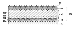
- FIG. 1 is a cross-sectional view showing the structure of a photoelectric conversion device 100 according to an embodiment of the present invention.
- the transparent insulating substrate 10 is a light incident side, the transparent conductive film 12 from the light incident side, and amorphous silicon (a-Si) having a wide band gap as a top cell (photoelectric conversion) Unit 102, intermediate layer 14, microcrystalline silicon ( ⁇ c-Si) (photoelectric conversion) unit 104 having a narrower band gap than a-Si unit 102 as a bottom cell, first back electrode layer 16, second back electrode layer 18, filler 20 and a protective film 22 are stacked.
- a-Si amorphous silicon having a wide band gap as a top cell (photoelectric conversion) Unit 102
- ⁇ c-Si microcrystalline silicon
- the transparent insulating substrate 10 for example, a material having transparency in at least a visible light wavelength region such as a glass substrate or a plastic substrate can be applied.
- a transparent conductive film 12 is formed on the transparent insulating substrate 10.
- the transparent conductive film 12 is doped with tin oxide (SnO 2 ), zinc oxide (ZnO), indium tin oxide (ITO), etc. with tin (Sn), antimony (Sb), fluorine (F), aluminum (Al), etc. It is preferable to use at least one or a combination of a plurality of transparent conductive oxides (TCO).
- zinc oxide (ZnO) is preferable because it has high translucency, low resistivity, and excellent plasma resistance.
- the transparent conductive film 12 can be formed by, for example, sputtering.
- the film thickness of the transparent conductive film 12 is preferably in the range of 0.5 ⁇ m to 5 ⁇ m. Moreover, it is preferable to provide unevenness having a light confinement effect on the surface of the transparent conductive film 12.
- an a-Si unit 102 is formed by sequentially laminating a p-type layer, an i-type layer, and an n-type silicon thin film.
- the a-Si unit 102 includes silicon-containing gas such as silane (SiH 4 ), disilane (Si 2 H 6 ), dichlorosilane (SiH 2 Cl 2 ), carbon-containing gas such as methane (CH 4 ), diborane (B 2 H 6 ) formed by plasma CVD in which a mixed gas obtained by mixing a p-type dopant-containing gas such as phosphine (PH 3 ) and a dilute gas such as phosphine (PH 3 ) and a diluent gas such as hydrogen (H 2 ) is formed into a plasma.
- silicon-containing gas such as silane (SiH 4 ), disilane (Si 2 H 6 ), dichlorosilane (SiH 2 Cl 2 ), carbon-containing gas such as methane (CH
- the RF plasma CVD for example, 13.56 MHz RF plasma CVD is preferably applied.
- the RF plasma CVD can be a parallel plate type. It is good also as a structure which provided the gas shower hole for supplying the mixed gas of a raw material in the side which does not arrange
- the input power density of plasma is preferably 5 mW / cm 2 or more and 100 mW / cm 2 or less.
- the p-type layer, i-type layer, and n-type layer are formed in separate film formation chambers.
- the film forming chamber can be evacuated by a vacuum pump and has an electrode for RF plasma CVD.
- a transfer device for the transparent insulating substrate 10, a power source and matching device for RF plasma CVD, piping for gas supply, and the like are attached.
- the p-type layer is formed on the transparent conductive film 12.
- the p-type layer is a p-type amorphous silicon layer (p-type a-Si: H) or p-type amorphous silicon carbide (p-type a-SiC: H) having a thickness of 10 nm to 100 nm doped with a p-type dopant (boron or the like). ).
- the film quality of the p-type layer can be changed by adjusting the mixing ratio of the silicon-containing gas, the carbon-containing gas, the p-type dopant-containing gas and the dilution gas, the pressure, and the high frequency power for plasma generation.
- the p-type layer includes a high-absorption amorphous silicon carbide layer (p1 layer) doped with boron at a high concentration, and a low-absorption amorphous silicon carbide layer (p2 layer) whose boron concentration is lower than that of the high-absorption amorphous silicon carbide layer. It is preferable to have a laminated structure. At this time, it is preferable to form a film by RF plasma CVD in which power is supplied at a power density of 11 mW / cm 2 with a substrate temperature of 180 ° C. and a reaction pressure of 80 Pa.
- the source gas is silane (SiH 4 ), methane (CH 4 ), hydrogen (H 2 ), and diborane (B 2 H 6 ), respectively, at 40 sccm, 80 sccm, It is preferable to supply at 400 sccm and 12 sccm (1% dilution).
- the source gas is silane (SiH 4 ), methane (CH 4 ), hydrogen (H 2 ), and diborane (B 2 H 6 ), respectively, at 40 sccm, 80 sccm, It is preferable to supply at 400 sccm and 1 sccm (1% dilution).
- the film thicknesses of the high absorption amorphous silicon carbide layer (p1 layer) and the low absorption amorphous silicon carbide layer (p2 layer) are preferably 7 nm and 3 nm, respectively.
- the i-type layer is an undoped amorphous silicon film of 50 nm to 500 nm formed on the p-type layer.
- the film quality of the i-type layer can be changed by adjusting the mixing ratio of the silicon-containing gas and the dilution gas, the pressure, and the high frequency power for plasma generation.
- the i-type layer serves as a power generation layer of the a-Si unit 102.
- the i-type layer preferably has a structure in which a top cell buffer layer that is an amorphous silicon carbide layer and a normal i-type layer that is an amorphous silicon layer are stacked.
- the top cell buffer layer is preferably formed by RF plasma CVD in which power is supplied at a power density of 11 mW / cm 2 under a source gas supply at a substrate temperature of 180 ° C. and a reaction pressure of 80 Pa.
- RF plasma CVD RF plasma CVD
- the film thickness of the top cell buffer layer is preferably 10 nm.
- a normal i-type layer that is an amorphous silicon layer is preferably formed by RF plasma CVD with power supplied at a power density of 11 mW / cm 2 under a source gas supply of 180 ° C. and a reaction pressure of 100 Pa. is there.
- silane (SiH 4 ) and hydrogen (H 2 ) are preferably supplied at 300 and 1000 sccm, respectively.
- the film thickness of a normal i-type layer is preferably 300 nm.
- the n-type layer is an n-type amorphous silicon layer (n-type a-Si: H) having a thickness of 10 nm to 100 nm doped with an n-type dopant (such as phosphorus) formed on the i-type layer or n-type microcrystalline silicon.
- Layer (n-type ⁇ c-Si: H) The film quality of the n-type layer can be changed by adjusting the mixing ratio of the silicon-containing gas, the carbon-containing gas, the n-type dopant-containing gas and the dilution gas, the pressure, and the high-frequency power for plasma generation.
- the n-type layer is preferably formed by RF plasma CVD in which power is supplied at a power density of 110 mW / cm 2 under the supply of a source gas having a substrate temperature of 180 ° C. and a reaction pressure of 200 Pa.
- a source gas having a substrate temperature of 180 ° C. and a reaction pressure of 200 Pa.
- silane (SiH 4 ), hydrogen (H 2 ), and phosphine (PH 3 ) at 10 sccm, 2000 sccm, and 5 sccm (1% dilution), respectively.
- the film thickness of the n-type layer is preferably 20 nm.
- the intermediate layer 14 is formed on the a-Si unit 102.
- the intermediate layer 14 is preferably made of a transparent conductive oxide (TCO) such as zinc oxide (ZnO) or silicon oxide (SiO x ).
- TCO transparent conductive oxide
- ZnO zinc oxide
- SiO x silicon oxide
- the intermediate layer 14 can be formed by, for example, sputtering.
- the film thickness of the intermediate layer 14 is preferably in the range of 10 nm to 200 nm. The intermediate layer 14 need not be provided.
- the ⁇ c-Si unit 104 includes silicon-containing gases such as silane (SiH 4 ), disilane (Si 2 H 6 ), dichlorosilane (SiH 2 Cl 2 ), carbon-containing gases such as methane (CH 4 ), diborane (B 2 H 6 ) formed by plasma CVD in which a mixed gas obtained by mixing a p-type dopant-containing gas such as phosphine (PH 3 ) and a dilute gas such as phosphine (PH 3 ) and a diluent gas such as hydrogen (H 2 ) is formed into a plasma.
- silicon-containing gases such as silane (SiH 4 ), disilane (Si 2 H 6 ), dichlorosilane (SiH 2 Cl 2 ), carbon-containing gases such as methane (CH 4 ), diborane (B 2 H 6 ) formed by plasma CVD in which a mixed gas obtained by mixing a p-type dopant-containing gas such as
- RF plasma CVD is preferably applied to the plasma CVD.
- the RF plasma CVD can be a parallel plate type. It is good also as a structure which provided the gas shower hole for supplying the mixed gas of a raw material in the side which does not arrange
- the input power density of plasma is preferably 5 mW / cm 2 or more and 100 mW / cm 2 or less.
- the p-type layer 40 is formed on the intermediate layer 14 or the n-type layer of the a-Si unit 102.
- at least two layers of a first p-type layer 40a that is a microcrystalline silicon layer and a second p-type layer 40b that is an amorphous layer are stacked.
- the amorphous layer is preferably an amorphous silicon layer (a-Si) or an amorphous silicon carbide layer (a-SiC).
- the first p-type layer 40a is preferably 5 nm to 50 nm in thickness.
- the film thickness is preferably 1 nm to 4.5 nm.
- the film thickness is preferably 1 nm or more and 4.5 nm or less.
- the film quality of the first p-type layer 40a and the second p-type layer 40b is adjusted by adjusting the mixing ratio of silicon-containing gas, carbon-containing gas, p-type dopant-containing gas and dilution gas, pressure, and high-frequency power for plasma generation. Can be changed.
- a treatment for oxidizing the second p-type layer 40b is performed.
- the transparent insulating substrate 10 is taken out from the vacuum layer of the film forming line and exposed to the atmosphere to be oxidized.
- the oxidation is preferably performed to such an extent that an oxygen atom concentration of 1 ⁇ 10 20 / cm 3 or more and 1 ⁇ 10 22 / cm 3 or less is detected in secondary ion mass spectrometry (SIMS).
- SIMS secondary ion mass spectrometry
- the primary ion species Cs + was irradiated with an acceleration voltage of 14.5 kV and a primary ion current of 15 nA at a vacuum degree of 1 ⁇ 10 ⁇ 7 Torr or less.
- an oxygen atom concentration of 1 ⁇ 10 20 / cm 3 or more and 1 ⁇ 10 22 / cm 3 or less is detected.
- the surface layer of the second p-type layer 40b is oxidized, and the i-type layer formed on the second p-type layer 40b.
- the interface level (defect level) at the interface with 42 is reduced, and the output voltage of the photoelectric conversion device 100 is improved.
- the method of performing the oxidation treatment by exposing the p-type layer 40b to the atmosphere there are many sheets that can be processed at one time for each forming apparatus of the a-Si unit 102 that is the top cell, and the ⁇ c-Si that is the bottom cell. This is particularly effective when the number of processed sheets per unit 104 is small. That is, after the a-Si unit and the p-type layer 40b are formed by the a-Si unit 102 forming apparatus, the a-Si unit 102 is once taken out from the a-Si unit 102 forming apparatus and exposed to the atmosphere. This is because the time until introduction into the forming apparatus can be used as the tact time adjustment time.
- the operating efficiency of the forming apparatus can be improved without increasing the number of forming apparatuses for the ⁇ c-Si unit 104. it can.
- the thickness of the p-type layer 40b is less than 1 nm, the effect of providing the p-type layer 40b is not sufficiently obtained. If the thickness is greater than 4.5 nm, the series resistance of the p-type layer 40 increases, and the short-circuit current and There is a risk of lowering the fill factor.
- a-SiC layer as the p-type layer 40b, a wider band gap can be achieved than when an a-Si layer is applied. Thereby, the open circuit voltage of the photoelectric conversion device 100 can be further increased, and the loss of light absorption in the p-type layer 40 can be reduced, so that the short circuit current is also improved.
- the i-type layer 42 is formed on the p-type layer 40.
- the i-type layer 42 is a microcrystalline silicon film which is formed on the p-type layer 40 and has a thickness of 0.5 ⁇ m or more and 5 ⁇ m or less which is not mainly doped.
- the i-type layer 42 is a layer that becomes a power generation layer of the ⁇ c-Si unit 104.
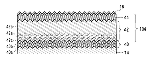
- the i-type layer 42 preferably has a configuration in which a buffer layer 42a is formed so as to be in contact with the p-type layer 40, and a main power generation layer 42b is formed on the buffer layer 42a.
- the buffer layer 42a is formed under a film formation condition that provides a higher crystallization rate than the film formation condition of the main power generation layer 42b.
- the buffer layer 42a is formed under film forming conditions such that the crystallization rate is higher than that of the main power generation layer 42b when it is formed as a single film on a glass substrate or the like.
- the buffer layer 42a may be a p-type layer to which a p-type dopant is added.
- the buffer layer 42a is formed by introducing a mixed gas having a hydrogen (H 2 ) / silane (SiH 4 ) dilution ratio of 130 or more and 800 or less at a pressure of 200 Pa by an RF plasma deposition method of 13.56 MHz. Is preferred.
- the substrate temperature during film formation was set to 80 ° C. or higher 250 ° C. or less, introducing power to the plasma is preferably set to 30 mW / cm 2 or more 1000 mW / cm 2 or less.
- the main power generation layer 42b is preferably formed by introducing a mixed gas having a hydrogen (H 2 ) / silane (SiH 4 ) dilution ratio of 30 or more and 200 or less at a pressure of 600 Pa by an RF plasma film forming method of 13.56 MHz. is there.
- the substrate temperature during film formation was set to 80 ° C. or higher 250 ° C. or less, introducing power to the plasma is preferably set to 30 mW / cm 2 or more 3000 mW / cm 2 or less.
- the film may be formed using VHF plasma of 27 MHz or the like.
- the buffer layer 42a By providing the buffer layer 42a, the crystallization rate in the vicinity of the interface of the p-type layer 40 in the i-type layer 42 is increased, and the crystallization rate of the entire i-type layer 42 serving as the power generation layer of the ⁇ c-Si unit 104 is also increased.
- the photoelectric conversion efficiency of the photoelectric conversion device 100 can be improved.
- the film thickness of the buffer layer 42a is preferably 8 nm or more and 100 nm or less. If the film thickness is less than 8 nm, the effect of inserting the buffer layer 42a is not sufficient, and if it is more than 100 nm, the photoelectric conversion characteristics such as the fill factor FF may be deteriorated.
- a buffer layer 42c which is an amorphous silicon layer may be provided between the p-type layer 40 and the buffer layer 42a.
- the buffer layer 42c may be formed under the general conditions for forming an amorphous silicon layer.
- a mixed gas having a hydrogen (H 2 ) / silane (SiH 4 ) dilution ratio of 10 or less is introduced at a pressure of 100 Pa.
- the substrate temperature during film formation is 80 ° C. or higher and 250 ° C. or lower, and the power introduced into the plasma is 5 mW / cm 2 or higher and 100 mW / cm 2 or lower.
- the film thickness of the buffer layer 42c is preferably 1 nm or more and 5 nm or less.
- the buffer layer 42c which is an amorphous silicon layer, between the p-type layer 40 and the buffer layer 42a as a base, the crystallization rate of the buffer layer 42a can be increased without being affected by the p-type layer 40. As a result, the series resistance of the ⁇ c-Si unit 104 can be reduced and the short-circuit current can be improved.
- At least one of the p-type layer 40 and the i-type layer 42 provided with the buffer layers 42a and 42c may be applied.
- both actions and effects can be obtained by applying both configurations simultaneously.
- the n-type layer 44 is formed on the i-type layer 42.
- the n-type layer 44 is an n-type microcrystalline silicon layer (n-type ⁇ c-Si: H) doped with an n-type dopant (such as phosphorus) and having a thickness of 5 nm to 50 nm.
- n-type dopant such as phosphorus
- the ⁇ c-Si unit 104 is not limited to this, and any unit that uses an i-type microcrystalline silicon layer (i-type ⁇ c-Si: H) described below as a power generation layer may be used.
- a laminated structure of a reflective metal and a transparent conductive oxide (TCO) is formed on the ⁇ c-Si unit 104 as the first back electrode layer 16 and the second back electrode layer 18.
- a transparent conductive oxide (TCO) such as tin oxide (SnO 2 ), zinc oxide (ZnO), indium tin oxide (ITO), or the like is used.
- the TCO can be formed by, for example, sputtering.
- metals such as silver (Ag) and aluminum (Al), can be used.
- the first back electrode layer 16 and the second back electrode layer 18 preferably have a thickness of about 1 ⁇ m in total. It is preferable that at least one of the first back electrode layer 16 and the second back electrode layer 18 is provided with unevenness for enhancing the light confinement effect.
- the surface of the second back electrode layer 18 is covered with the protective film 22 with the filler 20.
- the filler 20 and the protective film 22 can be made of a resin material such as EVA or polyimide. This can prevent moisture from entering the power generation layer of the photoelectric conversion device 100.
- a YAG laser fundamental wave 1064nm, double wave 532nm.
- the transparent insulating substrate 10 As the transparent insulating substrate 10, a glass substrate having a size of 33 cm ⁇ 43 cm square and 4 mm was used. On the transparent insulating substrate 10, 600 nm thick SnO 2 having a concavo-convex shape on the surface was formed as a transparent conductive film 12 by thermal CVD. Thereafter, the transparent conductive film 12 was patterned into strips with a YAG laser. A YAG laser having a wavelength of 1064 nm, an energy density of 13 J / cm 2 and a pulse frequency of 3 kHz was used.
- a p-type layer, an i-type layer, and an n-type layer of the a-Si unit 102 were sequentially stacked.
- the p-type layer, i-type layer, and n-type layer of the a-Si unit 102 were formed under the film formation conditions shown in Table 1.
- the transparent insulating substrate 10 was taken out from the film formation chamber to the atmosphere, and the n-type layer of the a-Si unit 102 was exposed to the atmosphere and oxidized.
- diborane (B 2 H 6 ) and phosphine (PH 3 ) are represented by a gas flow rate of 1% concentration on a hydrogen basis.
- the ⁇ c-Si unit 104 was formed on the n-type layer of the a-Si unit 102.
- the p-type layer 40, i-type layer 42, and n-type layer 44 of the ⁇ c-Si unit 104 were formed under the film formation conditions shown in Table 2.
- a YAG laser was irradiated to a position 50 ⁇ m lateral from the patterning position of the transparent conductive film 12, and the a-Si unit 102 and the ⁇ c-Si unit 104 were patterned into strips.
- a ZnO film was formed as the first back electrode layer 16 by sputtering, and an Ag electrode was formed as the second back electrode layer 18 by sputtering.
- a YAG laser was irradiated to a position 50 ⁇ m lateral from the patterning position of the a-Si unit 102 and the ⁇ c-Si unit 104, and the first back electrode layer 16 and the second back electrode layer 18 were patterned into strips.
- a YAG laser having an energy density of 0.7 J / cm 2 and a pulse frequency of 4 kHz was used.
- Comparative Example 2 A transparent conductive film 12 was formed on the transparent insulating substrate 10 in the same manner as in Comparative Example 1, and patterned into strips with a YAG laser. Next, a p-type layer, an i-type layer, and an n-type layer of the a-Si unit 102 were sequentially stacked. The p-type layer, i-type layer, and n-type layer of the a-Si unit 102 were formed under the deposition conditions shown in Table 3. Thereafter, the p-type layer 40 of the ⁇ c-Si unit 104 was formed as a single layer under the conditions shown in Table 3 without taking the transparent insulating substrate 10 from the film formation chamber into the atmosphere.
- the transparent insulating substrate 10 was taken out from the film formation chamber to the atmosphere, and the p-type layer 40 of the ⁇ c-Si unit 104 formed as a single layer was exposed to the atmosphere and oxidized. Subsequently, the ⁇ c-Si unit 104 was formed on the p-type layer 40 of the oxidized ⁇ c-Si unit 104.
- the i-type layer 42 and the n-type layer 44 of the ⁇ c-Si unit 104 were formed under the film formation conditions shown in Table 4.
- Example 1 A transparent conductive film 12 was formed on the transparent insulating substrate 10 in the same manner as in Comparative Example 1, and patterned into strips with a YAG laser. Next, a p-type layer, an i-type layer, and an n-type layer of the a-Si unit 102 were sequentially stacked. The p-type layer, i-type layer, and n-type layer of the a-Si unit 102 were formed under the deposition conditions shown in Table 5. Thereafter, the first p-type layer 40a and the second p-type layer 40b of the ⁇ c-Si unit 104 were formed under the conditions shown in Table 5 without taking the transparent insulating substrate 10 from the film formation chamber into the atmosphere.
- the transparent insulating substrate 10 was taken out from the film formation chamber to the atmosphere, and the second p-type layer 40b of the ⁇ c-Si unit 104 was exposed to the atmosphere to be oxidized. Subsequently, the ⁇ c-Si unit 104 was formed on the oxidized second p-type layer 40b.
- the i-type layer 42 and the n-type layer 44 of the ⁇ c-Si unit 104 were formed under the film formation conditions shown in Table 4 as in Comparative Example 2. Thereafter, similarly to Comparative Example 1, formation and patterning of the first back electrode layer 16 and the second back electrode layer 18 were performed.
- the transparent conductive film 12 Similar to the first embodiment, the transparent conductive film 12, the p-type layer of the a-Si unit 102, the i-type layer and the n-type layer, and the first p-type layer 40a and the first p-type layer 40a of the ⁇ c-Si unit 104 are formed on the transparent insulating substrate 10. Two p-type layers 40b were formed. Next, the transparent insulating substrate 10 was taken out from the film formation chamber to the atmosphere, and the second p-type layer 40b of the ⁇ c-Si unit 104 was exposed to the atmosphere and oxidized.
- the ⁇ c-Si unit 104 was formed on the oxidized second p-type layer 40b.
- the i-type layer 42 was formed by laminating the buffer layer 42 a and the main power generation layer 42 b of the ⁇ c-Si unit 104, and the n-type layer 44 was formed on the i-type layer 42.
- the i-type layer 42 and the n-type layer 44 were formed under the film formation conditions shown in Table 6. Thereafter, similarly to Comparative Example 1, formation and patterning of the first back electrode layer 16 and the second back electrode layer 18 were performed.
- Example 3 The transparent conductive film 12 and the p-type layer, i-type layer, and n-type layer of the a-Si unit 102 were formed on the transparent insulating substrate 10 in the same manner as in Example 1. Further, as shown in Table 7, the first p-type layer 40a and the second p-type layer 40b of the ⁇ c-Si unit 104 were formed. Here, the second p-type layer 40b is an amorphous silicon carbide layer. Next, the transparent insulating substrate 10 was taken out from the film formation chamber to the atmosphere, and the second p-type layer 40b of the ⁇ c-Si unit 104 was exposed to the atmosphere and oxidized.
- the ⁇ c-Si unit 104 was formed on the oxidized second p-type layer 40b.
- the i-type layer 42 and the n-type layer 44 were formed under the film formation conditions shown in Table 6 in the same manner as in Example 2. Thereafter, similarly to Comparative Example 1, formation and patterning of the first back electrode layer 16 and the second back electrode layer 18 were performed.
- Example 4 Similar to the third embodiment, the transparent conductive film 12, the p-type layer of the a-Si unit 102, the i-type layer and the n-type layer, and the first p-type layer 40a and the first p-type layer 40a of the ⁇ c-Si unit 104 are formed on the transparent insulating substrate 10. Two p-type layers 40b were formed. Next, the transparent insulating substrate 10 was taken out from the film formation chamber to the atmosphere, and the second p-type layer 40b of the ⁇ c-Si unit 104 was exposed to the atmosphere and oxidized.
- the ⁇ c-Si unit 104 was formed on the oxidized second p-type layer 40b.
- the buffer layer 42 a, the buffer layer 42 c and the main power generation layer 42 b of the ⁇ c-Si unit 104 were stacked to form the i-type layer 42, and the n-type layer 44 was formed on the i-type layer 42.
- the i-type layer 42 and the n-type layer 44 were formed under the film formation conditions shown in Table 8. Thereafter, similarly to Comparative Example 1, formation and patterning of the first back electrode layer 16 and the second back electrode layer 18 were performed.
- the transparent conductive film 12, the p-type layer of the a-Si unit 102, the i-type layer and the n-type layer, and the first p-type layer 40a and the first p-type layer 40a of the ⁇ c-Si unit 104 are formed on the transparent insulating substrate 10. Two p-type layers 40b were formed. Next, the transparent insulating substrate 10 was taken out from the film formation chamber to the atmosphere, and the second p-type layer 40b of the ⁇ c-Si unit 104 was exposed to the atmosphere and oxidized.
- the ⁇ c-Si unit 104 was formed on the oxidized second p-type layer 40b.
- the ⁇ c-Si unit 104 forms the i-type layer 42 by stacking the buffer layer 42a and the main power generation layer 42b on the second p-type layer 40b under the film formation conditions shown in Table 9.
- An n-type layer 44 was formed.
- boron which is a p-type dopant, is added to the buffer layer 42a to form a p-type layer.
- formation and patterning of the first back electrode layer 16 and the second back electrode layer 18 were performed.
- Example 6 In Example 3, the film thickness dependency of the second p-type layer 40b was examined and determined as Example 6. In addition to the case where the second p-type layer 40b was not provided, the photoelectric conversion efficiency was measured when the thickness of the second p-type layer 40b was changed from 1 nm to 10 nm.
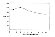
- Example 7 In Example 3, the film thickness dependency of the buffer layer 42a was examined and determined as Example 6. In addition to the case where the buffer layer 42a was not provided, the photoelectric conversion efficiency was measured when the thickness of the buffer layer 42a was changed to 300 nm.
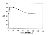
- Example 8 In Example 3, the dependency of the hydrogen (H 2 ) / silane (SiH 4 ) dilution ratio upon formation of the buffer layer 42 a was examined and determined as Example 8. The dilution ratio of hydrogen (H 2 ) / silane (SiH 4 ) was varied in the range of 50 to 400.
- Comparative Example 3 A transparent conductive film 12 was formed on the transparent insulating substrate 10 in the same manner as in Comparative Example 1, and patterned into strips with a YAG laser. Next, without forming the a-Si unit 102, the p-type layer 40, the i-type layer 42, and the n-type layer 44 of the ⁇ c-Si unit 104 were formed under the film forming conditions shown in Table 2. Thereafter, similarly to Comparative Example 1, formation and patterning of the first back electrode layer 16 and the second back electrode layer 18 were performed.
- Example 9 A transparent conductive film 12 was formed on the transparent insulating substrate 10 in the same manner as in Comparative Example 1, and patterned into strips with a YAG laser. Next, without forming the a-Si unit 102, the first p-type layer 40a and the second p-type layer 40b are formed under the film formation conditions shown in Table 7, and the second p-type layer 40b is placed in the atmosphere. After exposure and oxidation, the i-type layer 42 and the n-type layer 44 of the ⁇ c-Si unit 104 were formed under the film formation conditions shown in Table 6. Thereafter, similarly to Comparative Example 1, formation and patterning of the first back electrode layer 16 and the second back electrode layer 18 were performed.
- Example 10 A transparent conductive film 12 was formed on the transparent insulating substrate 10 in the same manner as in Comparative Example 1, and patterned into strips with a YAG laser. Next, an a-Si unit 102 was formed as in Comparative Example 1. Thereafter, after taking out once into the atmosphere, as shown in Table 10, a p-type semiconductor layer of the ⁇ c-Si unit 104 was formed. For the p-type layer, a p-type amorphous silicon carbide semiconductor layer was formed after forming a p-type crystalline silicon semiconductor layer. Subsequently, an i-type microcrystalline silicon layer (buffer layer), an i-type microcrystalline silicon layer, and an n-type crystalline silicon layer were formed. Thereafter, similarly to Comparative Example 1, formation and patterning of the first back electrode layer 16 and the second back electrode layer 18 were performed.
- Table 11 shows the results of measuring open circuit voltage Voc, short circuit current density Jsc, fill factor FF, and photoelectric conversion efficiency ⁇ for the photoelectric conversion devices of Comparative Examples 1 and 2 and Examples 1 to 5.
- the measurement result of Comparative Example 1 is set to 1, and the measurement results of Comparative Example 2 and Examples 1 to 5 are normalized.
- Example 1 although the short circuit current density Jsc and the fill factor FF are lower than those of Comparative Examples 1 and 2, the open circuit voltage Voc is increased by 1%, and the effect of inserting the second p-type layer 40b is obtained. It has been. Further, in Example 2, by inserting the buffer layer 42a into the i-type layer 42 of the ⁇ c-Si unit 104, in addition to the improvement of the open circuit voltage Voc, the decrease of the fill factor FF is suppressed, and the photoelectric conversion efficiency ⁇ is Compared to Comparative Example 1, it was improved by 5%. Further, in Example 3, the open circuit voltage Voc and the short circuit current density Jsc increased compared to Example 2, and the photoelectric conversion efficiency ⁇ was improved by 7% compared to Comparative Example 1.
- Example 4 the short circuit current density Jsc increased compared with Example 3, and the photoelectric conversion efficiency (eta) improved 10% with respect to the comparative example 1.
- Example 5 the open circuit voltage Voc and the short circuit current density Jsc increased compared with the comparative example 1, and the photoelectric conversion efficiency (eta) improved 5% with respect to the comparative example 1.
- the film thickness dependence of the second p-type layer 40b in Example 6 is that the photoelectric conversion efficiency ⁇ is 90% or more of the maximum value when the film thickness is in the range of 1 nm to 4.5 nm.
- the photoelectric conversion efficiency showed a high value.
- the film thickness was larger than 4.5 nm, the series resistance value of the photoelectric conversion device increased and the characteristics deteriorated.
- the film thickness dependence of the buffer layer 42a in Example 7 has a maximum photoelectric conversion efficiency ⁇ when the film thickness is 30 nm, and a high value in the range of the film thickness from 10 nm to 50 nm. showed that.
- the photoelectric conversion efficiency ⁇ was maintained at 90% or more of the maximum value, and a sufficient characteristic improvement was obtained.
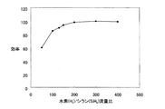
- the dependency of the hydrogen (H 2 ) / silane (SiH 4 ) dilution ratio upon formation of the buffer layer 42a in Example 8 is that the photoelectric conversion efficiency ⁇ is maximum when the dilution ratio is around 250 times as shown in FIG. It became. Further, when the dilution ratio was 130 times or more, the photoelectric conversion efficiency ⁇ was maintained at about 90% or more of the maximum value, and a sufficient characteristic improvement was obtained. On the other hand, if the dilution ratio is greater than 800 times, a sufficient film formation speed cannot be obtained from the relationship between the film thickness of the buffer layer 42a and the production tact time, so the dilution ratio is preferably 800 times or less.
- Table 12 shows the results of measuring the open-circuit voltage Voc, the short-circuit current density Jsc, the fill factor FF, and the photoelectric conversion efficiency ⁇ for the photoelectric conversion devices of Comparative Example 3 and Example 9.
- the measurement result of Comparative Example 3 is set to 1, and the measurement result of Example 9 is normalized and shown.
- Example 9 the open circuit voltage Voc and the short-circuit current density Jsc increased compared to Comparative Example 3, and the photoelectric conversion efficiency ⁇ improved by 6% compared to Comparative Example 3.
- the present invention is effective not only in the tandem photoelectric conversion device including the a-Si unit 102 and the ⁇ c-Si unit 104 but also in the single-type photoelectric conversion device including only the ⁇ c-Si unit 104. is there.
- Example 10 the open-circuit voltage Voc and the short-circuit current density Jsc increased compared to Comparative Example 1, and the photoelectric conversion efficiency ⁇ improved by 3% compared to Comparative Example 1.
- the a-Si unit 102 is formed, it is exposed to the atmosphere, and after forming the p-type crystalline silicon semiconductor layer as the p-type layer of the ⁇ c-Si unit 104, a p-type amorphous silicon carbide semiconductor layer is formed. Subsequently, the present invention is effective even when an i-type microcrystalline silicon layer (buffer layer) is formed.
- a-Si unit amorphous silicon photoelectric conversion unit
- ⁇ c-Si unit microcrystalline silicon photoelectric conversion Unit
Landscapes
- Engineering & Computer Science (AREA)
- General Physics & Mathematics (AREA)
- Sustainable Energy (AREA)
- Physics & Mathematics (AREA)
- Condensed Matter Physics & Semiconductors (AREA)
- Electromagnetism (AREA)
- Life Sciences & Earth Sciences (AREA)
- Computer Hardware Design (AREA)
- Microelectronics & Electronic Packaging (AREA)
- Power Engineering (AREA)
- Chemical & Material Sciences (AREA)
- Crystallography & Structural Chemistry (AREA)
- Photovoltaic Devices (AREA)
Abstract
L'invention a pour objet d'augmenter le rendement de conversion photoélectrique dans un dispositif de conversion photoélectrique, et décrit un dispositif de conversion photoélectrique contenant une unité de conversion photoélectrique dans laquelle une couche de type p (40) contenant un dopant de type p, une couche de type i (42) qui est une couche de silicium microcristallin qui est une couche produisant de l'électricité et une couche de type n (44) contenant un dopant de type n sont disposées en couches, la couche de type p (40) étant amenée à avoir une structure en couches comprenant une première couche de type p (40a) qui est une couche de silicium microcristallin et une seconde couche de type p (40b) contenant une couche de type p de carbure de silicium amorphe et/ou une couche de type p de silicium amorphe disposée entre la couche de type p de silicium microcristallin (40a) et la couche de type i (42). La seconde couche de type p (40b) est dotée d'une couche d'oxyde du côté de la couche de type i (42).
Priority Applications (2)
| Application Number | Priority Date | Filing Date | Title |
|---|---|---|---|
| CN2010800568363A CN102668111A (zh) | 2009-12-15 | 2010-12-13 | 光电转换装置和其制造方法 |
| US13/523,323 US8575472B2 (en) | 2009-12-15 | 2012-06-14 | Photoelectric conversion device and method for producing same |
Applications Claiming Priority (2)
| Application Number | Priority Date | Filing Date | Title |
|---|---|---|---|
| JP2009-283877 | 2009-12-15 | ||
| JP2009283877A JP4940290B2 (ja) | 2009-12-15 | 2009-12-15 | 光電変換装置及びその製造方法 |
Related Child Applications (1)
| Application Number | Title | Priority Date | Filing Date |
|---|---|---|---|
| US13/523,323 Continuation US8575472B2 (en) | 2009-12-15 | 2012-06-14 | Photoelectric conversion device and method for producing same |
Publications (1)
| Publication Number | Publication Date |
|---|---|
| WO2011074523A1 true WO2011074523A1 (fr) | 2011-06-23 |
Family
ID=44167275
Family Applications (1)
| Application Number | Title | Priority Date | Filing Date |
|---|---|---|---|
| PCT/JP2010/072346 WO2011074523A1 (fr) | 2009-12-15 | 2010-12-13 | Dispositif de conversion photoélectrique et son procédé de production |
Country Status (4)
| Country | Link |
|---|---|
| US (1) | US8575472B2 (fr) |
| JP (1) | JP4940290B2 (fr) |
| CN (1) | CN102668111A (fr) |
| WO (1) | WO2011074523A1 (fr) |
Cited By (4)
| Publication number | Priority date | Publication date | Assignee | Title |
|---|---|---|---|---|
| WO2013065538A1 (fr) * | 2011-11-03 | 2013-05-10 | 三洋電機株式会社 | Dispositif de conversion photoélectrique |
| US20150107668A1 (en) * | 2012-06-29 | 2015-04-23 | Sanyo Electric Co., Ltd. | Solar cell |
| CN114678434A (zh) * | 2021-12-28 | 2022-06-28 | 浙江爱旭太阳能科技有限公司 | 一种提高光电转换效率的异质结电池 |
| CN114678434B (zh) * | 2021-12-28 | 2024-05-10 | 浙江爱旭太阳能科技有限公司 | 一种提高光电转换效率的异质结电池 |
Families Citing this family (7)
| Publication number | Priority date | Publication date | Assignee | Title |
|---|---|---|---|---|
| JP5927027B2 (ja) * | 2011-10-05 | 2016-05-25 | 株式会社半導体エネルギー研究所 | 光電変換装置 |
| KR101918737B1 (ko) * | 2012-03-19 | 2019-02-08 | 엘지전자 주식회사 | 태양 전지 |
| CN102931270B (zh) * | 2012-11-19 | 2015-09-02 | 深圳市创益科技发展有限公司 | 一种弱光型非晶硅太阳能电池及其制造方法 |
| KR101979843B1 (ko) * | 2013-03-13 | 2019-05-17 | 엘지전자 주식회사 | 태양전지 |
| JP5892113B2 (ja) * | 2013-06-26 | 2016-03-23 | 株式会社ダイフク | 物品保管設備 |
| JP6350979B2 (ja) * | 2013-09-04 | 2018-07-04 | パナソニックIpマネジメント株式会社 | 太陽電池 |
| WO2017057646A1 (fr) * | 2015-09-30 | 2017-04-06 | 株式会社カネカ | Dispositif de conversion photoélectrique multi-jonction et module de conversion photoélectrique |
Citations (7)
| Publication number | Priority date | Publication date | Assignee | Title |
|---|---|---|---|---|
| JP2000077694A (ja) * | 1998-06-16 | 2000-03-14 | Canon Inc | 光起電力素子および太陽電池モジュ―ル |
| JP2003158276A (ja) * | 2001-11-21 | 2003-05-30 | Mitsubishi Heavy Ind Ltd | 微結晶シリコン太陽電池及びその製造方法 |
| JP2003188400A (ja) * | 2001-12-20 | 2003-07-04 | Mitsubishi Heavy Ind Ltd | 結晶性SiC膜の製造方法、結晶性SiC膜及び太陽電池 |
| JP2004179371A (ja) * | 2002-11-27 | 2004-06-24 | Mitsubishi Heavy Ind Ltd | 薄膜太陽電池,及びその製造方法 |
| JP2004335823A (ja) * | 2003-05-09 | 2004-11-25 | Canon Inc | 光起電力素子及び光起電力素子の形成方法 |
| JP2007243142A (ja) * | 2006-03-08 | 2007-09-20 | National Science & Technology Development Agency | 薄膜太陽電池とその加工処理 |
| JP2008283075A (ja) * | 2007-05-11 | 2008-11-20 | Kaneka Corp | 光電変換装置の製造方法 |
Family Cites Families (6)
| Publication number | Priority date | Publication date | Assignee | Title |
|---|---|---|---|---|
| JP4033517B2 (ja) | 1997-04-17 | 2008-01-16 | 株式会社カネカ | シリコン系薄膜光電変換装置 |
| JP4158267B2 (ja) * | 1999-03-15 | 2008-10-01 | 富士電機ホールディングス株式会社 | 非単結晶太陽電池 |
| JP2005197608A (ja) * | 2004-01-09 | 2005-07-21 | Mitsubishi Heavy Ind Ltd | 光電変換装置 |
| EP2099076A4 (fr) * | 2006-12-25 | 2013-07-03 | Sharp Kk | Convertisseur photoélectrique et procédé de fabrication de celui-ci |
| CN101471387B (zh) * | 2007-12-27 | 2012-07-11 | 财团法人工业技术研究院 | 光电转换元件的p型掺杂层及其制造方法 |
| CN101295746A (zh) * | 2008-04-15 | 2008-10-29 | 福建钧石能源有限公司 | 薄膜太阳能电池及其制造方法 |
-
2009
- 2009-12-15 JP JP2009283877A patent/JP4940290B2/ja not_active Expired - Fee Related
-
2010
- 2010-12-13 WO PCT/JP2010/072346 patent/WO2011074523A1/fr active Application Filing
- 2010-12-13 CN CN2010800568363A patent/CN102668111A/zh active Pending
-
2012
- 2012-06-14 US US13/523,323 patent/US8575472B2/en not_active Expired - Fee Related
Patent Citations (7)
| Publication number | Priority date | Publication date | Assignee | Title |
|---|---|---|---|---|
| JP2000077694A (ja) * | 1998-06-16 | 2000-03-14 | Canon Inc | 光起電力素子および太陽電池モジュ―ル |
| JP2003158276A (ja) * | 2001-11-21 | 2003-05-30 | Mitsubishi Heavy Ind Ltd | 微結晶シリコン太陽電池及びその製造方法 |
| JP2003188400A (ja) * | 2001-12-20 | 2003-07-04 | Mitsubishi Heavy Ind Ltd | 結晶性SiC膜の製造方法、結晶性SiC膜及び太陽電池 |
| JP2004179371A (ja) * | 2002-11-27 | 2004-06-24 | Mitsubishi Heavy Ind Ltd | 薄膜太陽電池,及びその製造方法 |
| JP2004335823A (ja) * | 2003-05-09 | 2004-11-25 | Canon Inc | 光起電力素子及び光起電力素子の形成方法 |
| JP2007243142A (ja) * | 2006-03-08 | 2007-09-20 | National Science & Technology Development Agency | 薄膜太陽電池とその加工処理 |
| JP2008283075A (ja) * | 2007-05-11 | 2008-11-20 | Kaneka Corp | 光電変換装置の製造方法 |
Cited By (5)
| Publication number | Priority date | Publication date | Assignee | Title |
|---|---|---|---|---|
| WO2013065538A1 (fr) * | 2011-11-03 | 2013-05-10 | 三洋電機株式会社 | Dispositif de conversion photoélectrique |
| US20150107668A1 (en) * | 2012-06-29 | 2015-04-23 | Sanyo Electric Co., Ltd. | Solar cell |
| DE112012006605B4 (de) | 2012-06-29 | 2021-10-14 | Panasonic Intellectual Property Management Co., Ltd. | Solarzelle |
| CN114678434A (zh) * | 2021-12-28 | 2022-06-28 | 浙江爱旭太阳能科技有限公司 | 一种提高光电转换效率的异质结电池 |
| CN114678434B (zh) * | 2021-12-28 | 2024-05-10 | 浙江爱旭太阳能科技有限公司 | 一种提高光电转换效率的异质结电池 |
Also Published As
| Publication number | Publication date |
|---|---|
| JP4940290B2 (ja) | 2012-05-30 |
| US8575472B2 (en) | 2013-11-05 |
| US20120266948A1 (en) | 2012-10-25 |
| JP2011129561A (ja) | 2011-06-30 |
| CN102668111A (zh) | 2012-09-12 |
Similar Documents
| Publication | Publication Date | Title |
|---|---|---|
| JP4940290B2 (ja) | 光電変換装置及びその製造方法 | |
| JP4902779B2 (ja) | 光電変換装置及びその製造方法 | |
| JP2006310503A (ja) | 積層型光起電力装置 | |
| JP4767365B2 (ja) | 薄膜太陽電池及びその製造方法 | |
| JP2010283161A (ja) | 太陽電池及びその製造方法 | |
| WO2010023991A1 (fr) | Procédé de production d’un dispositif de conversion photoélectrique, dispositif de conversion photoélectrique, et système de production d’un dispositif de conversion photoélectrique | |
| JP5232362B2 (ja) | 集積化薄膜光電変換装置の製造方法および、その製造方法で得られうる集積化薄膜光電変換装置。 | |
| WO2010050035A1 (fr) | Procédé de fabrication d'un appareil de conversion photoélectrique | |
| JP4712127B2 (ja) | 太陽電池の製造方法及び製造装置 | |
| JP2008283075A (ja) | 光電変換装置の製造方法 | |
| JP2011014619A (ja) | 太陽電池及びその製造方法 | |
| JP5373045B2 (ja) | 光電変換装置 | |
| JP2011014618A (ja) | 太陽電池及びその製造方法 | |
| WO2011105166A1 (fr) | Module de conversion photoélectrique et son procédé de fabrication | |
| JP2010283162A (ja) | 太陽電池及びその製造方法 | |
| JP4875566B2 (ja) | 光電変換装置の製造方法 | |
| US20100307573A1 (en) | Solar cell and manufacturing method thereof | |
| JP2011216586A (ja) | 積層型光電変換装置および積層型光電変換装置の製造方法 | |
| WO2010146846A1 (fr) | Dispositif de conversion photoélectrique et procédé de production d'un dispositif de conversion photoélectrique | |
| WO2013065538A1 (fr) | Dispositif de conversion photoélectrique | |
| JP2011077220A (ja) | 太陽電池 | |
| WO2011148724A1 (fr) | Couche intermédiaire pour dispositif de conversion photoélectrique de type laminat, dispositif de conversion photoélectrique de type laminat et procédé de production du dispositif de conversion photoélectrique de type laminat | |
| WO2013080803A1 (fr) | Dispositif d'énergie photovoltaïque | |
| JP2010283159A (ja) | 太陽電池及びその製造方法 | |
| JP2002280584A (ja) | ハイブリッド型薄膜光電変換装置とその製造方法 |
Legal Events
| Date | Code | Title | Description |
|---|---|---|---|
| WWE | Wipo information: entry into national phase |
Ref document number: 201080056836.3 Country of ref document: CN |
|
| 121 | Ep: the epo has been informed by wipo that ep was designated in this application |
Ref document number: 10837549 Country of ref document: EP Kind code of ref document: A1 |
|
| NENP | Non-entry into the national phase |
Ref country code: DE |
|
| 122 | Ep: pct application non-entry in european phase |
Ref document number: 10837549 Country of ref document: EP Kind code of ref document: A1 |