WO2011040480A1 - 回路基板 - Google Patents
回路基板 Download PDFInfo
- Publication number
- WO2011040480A1 WO2011040480A1 PCT/JP2010/066972 JP2010066972W WO2011040480A1 WO 2011040480 A1 WO2011040480 A1 WO 2011040480A1 JP 2010066972 W JP2010066972 W JP 2010066972W WO 2011040480 A1 WO2011040480 A1 WO 2011040480A1
- Authority
- WO
- WIPO (PCT)
- Prior art keywords
- electrode pattern
- circuit board
- mounting
- core substrate
- pattern
- Prior art date
Links
Images


Classifications
-
- H—ELECTRICITY
- H05—ELECTRIC TECHNIQUES NOT OTHERWISE PROVIDED FOR
- H05K—PRINTED CIRCUITS; CASINGS OR CONSTRUCTIONAL DETAILS OF ELECTRIC APPARATUS; MANUFACTURE OF ASSEMBLAGES OF ELECTRICAL COMPONENTS
- H05K3/00—Apparatus or processes for manufacturing printed circuits
- H05K3/30—Assembling printed circuits with electric components, e.g. with resistor
- H05K3/32—Assembling printed circuits with electric components, e.g. with resistor electrically connecting electric components or wires to printed circuits
- H05K3/34—Assembling printed circuits with electric components, e.g. with resistor electrically connecting electric components or wires to printed circuits by soldering
- H05K3/3452—Solder masks
-
- H—ELECTRICITY
- H05—ELECTRIC TECHNIQUES NOT OTHERWISE PROVIDED FOR
- H05K—PRINTED CIRCUITS; CASINGS OR CONSTRUCTIONAL DETAILS OF ELECTRIC APPARATUS; MANUFACTURE OF ASSEMBLAGES OF ELECTRICAL COMPONENTS
- H05K2201/00—Indexing scheme relating to printed circuits covered by H05K1/00
- H05K2201/09—Shape and layout
- H05K2201/09818—Shape or layout details not covered by a single group of H05K2201/09009 - H05K2201/09809
- H05K2201/09909—Special local insulating pattern, e.g. as dam around component
-
- H—ELECTRICITY
- H05—ELECTRIC TECHNIQUES NOT OTHERWISE PROVIDED FOR
- H05K—PRINTED CIRCUITS; CASINGS OR CONSTRUCTIONAL DETAILS OF ELECTRIC APPARATUS; MANUFACTURE OF ASSEMBLAGES OF ELECTRICAL COMPONENTS
- H05K2201/00—Indexing scheme relating to printed circuits covered by H05K1/00
- H05K2201/10—Details of components or other objects attached to or integrated in a printed circuit board
- H05K2201/10613—Details of electrical connections of non-printed components, e.g. special leads
- H05K2201/10621—Components characterised by their electrical contacts
- H05K2201/10636—Leadless chip, e.g. chip capacitor or resistor
-
- H—ELECTRICITY
- H05—ELECTRIC TECHNIQUES NOT OTHERWISE PROVIDED FOR
- H05K—PRINTED CIRCUITS; CASINGS OR CONSTRUCTIONAL DETAILS OF ELECTRIC APPARATUS; MANUFACTURE OF ASSEMBLAGES OF ELECTRICAL COMPONENTS
- H05K2203/00—Indexing scheme relating to apparatus or processes for manufacturing printed circuits covered by H05K3/00
- H05K2203/13—Moulding and encapsulation; Deposition techniques; Protective layers
- H05K2203/1305—Moulding and encapsulation
- H05K2203/1316—Moulded encapsulation of mounted components
-
- H—ELECTRICITY
- H05—ELECTRIC TECHNIQUES NOT OTHERWISE PROVIDED FOR
- H05K—PRINTED CIRCUITS; CASINGS OR CONSTRUCTIONAL DETAILS OF ELECTRIC APPARATUS; MANUFACTURE OF ASSEMBLAGES OF ELECTRICAL COMPONENTS
- H05K3/00—Apparatus or processes for manufacturing printed circuits
- H05K3/22—Secondary treatment of printed circuits
- H05K3/28—Applying non-metallic protective coatings
- H05K3/284—Applying non-metallic protective coatings for encapsulating mounted components
-
- Y—GENERAL TAGGING OF NEW TECHNOLOGICAL DEVELOPMENTS; GENERAL TAGGING OF CROSS-SECTIONAL TECHNOLOGIES SPANNING OVER SEVERAL SECTIONS OF THE IPC; TECHNICAL SUBJECTS COVERED BY FORMER USPC CROSS-REFERENCE ART COLLECTIONS [XRACs] AND DIGESTS
- Y02—TECHNOLOGIES OR APPLICATIONS FOR MITIGATION OR ADAPTATION AGAINST CLIMATE CHANGE
- Y02P—CLIMATE CHANGE MITIGATION TECHNOLOGIES IN THE PRODUCTION OR PROCESSING OF GOODS
- Y02P70/00—Climate change mitigation technologies in the production process for final industrial or consumer products
- Y02P70/50—Manufacturing or production processes characterised by the final manufactured product
Definitions
- the present invention relates to a circuit board in which a chip component is mounted on a core substrate on which an electrode pattern is formed, and a resin layer is further provided thereon, and more specifically, the adhesion strength between the core substrate and the resin layer is improved. It relates to a measured circuit board.
- the core substrate is disclosed in, for example, Japanese Patent Application Laid-Open No. 9-148722.
- regions other than the mounting electrode pattern to which the terminal electrodes of the chip components are soldered are often covered with a resist pattern.
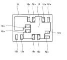
- FIG. 8 to 11 show a conventional circuit board having such a structure.
- 8 and FIG. 9 are exploded plan views
- FIG. 10 is a plan view
- FIG. 11 is a schematic cross-sectional view taken along the chain line CC in FIG. 10
- FIG. 8 shows the chip substrate and resist pattern removed from this circuit board.
- FIG. 9 shows a state where the chip parts are removed.
- reference numeral 11 denotes a core substrate, which includes a printed circuit board in which a glass fiber is impregnated with an epoxy resin.
- An electrode pattern 12 made of a metal film such as copper is formed on the first main surface (upper surface) of the core substrate 11.
- the electrode pattern 12 is formed, for example, by attaching a metal foil to the entire first main surface of the core substrate 11 and etching it.
- the electrode pattern 12 is divided into a mounting electrode pattern, a connection electrode pattern, a ground electrode pattern, and the like to which the terminal electrode of the chip electrode is soldered according to its function.
- a resist pattern 13 having a desired shape is formed on the electrode pattern 12 on a region other than the mounting electrode pattern 12a to which the terminal electrode of the chip component is soldered.
- the resist pattern 13 is formed, for example, by applying a resist ink in a desired shape, drying, and developing.
- the terminal electrode of the chip component 14 is joined to the mounting electrode pattern 12a by solder (not shown).
- solder for joining the terminal electrode of the chip component 14 to the mounting electrode pattern 12a, for example, a solder paste is applied on the mounting electrode pattern 12a, and the terminal electrode is positioned on the mounting electrode pattern 12a. This is done by mounting the chip component 14 and heating and cooling.
- the region other than the mounting electrode pattern 12a in the electrode pattern 12 is covered with the resist pattern 13 because the melted solder is mounted when the chip component 14 is mounted on the mounting electrode pattern 12a.
- the purpose is to block outflow and flow on the electrode pattern 12, and to protect the region other than the mounting electrode pattern 12a from the outside of the electrode pattern 12 to improve moisture resistance and rust prevention. It is.
- a resin layer is further provided on a core board on which chip components are mounted.
- FIG. 12 shows a circuit board in which a resin layer is further provided on the conventional circuit board shown in FIGS.
- FIG. 12 is a schematic cross-sectional view showing a portion corresponding to the chain line CC portion of FIG.
- an electrode pattern 12 and a solder resist 13 are formed, and a resin layer 15 is further formed on the core substrate 11 on which the chip component 14 is mounted.
- the resin layer 15 functions to protect the chip component 14 from the outside and to improve the strength of the entire circuit board.
- this circuit board has a problem that the adhesion strength between the core substrate 11 and the resin layer 15 is small. This is because a region other than the mounting electrode pattern 12 a in the electrode pattern 12 is covered with the resist pattern 13. That is, in general, since the surface of the resist pattern 13 is smooth, the anchoring force with respect to the resin layer 15 is smaller and the adhesion strength with the resin layer 15 is smaller than the metal film constituting the electrode pattern 12. is there. Therefore, when this circuit board is mounted on another large circuit board, if this circuit board is in a moisture absorbing state, delamination occurs at the interface between the resist pattern 13 and the resin layer 15 having low adhesion strength. There was a fear.
- the present invention has been made to solve the above-described problems of the conventional circuit board, and as its means, the circuit board of the present invention is provided on the core substrate and the first main surface of the core substrate.
- an electrode pattern including a mounting electrode pattern is formed on the first main surface of the core substrate, and the mounting electrode pattern is formed by partitioning a part of the electrode pattern with a line resist pattern. I did it.
- the surface roughness of the region not partitioned by the mounting electrode pattern is larger than the surface roughness of the mounting electrode pattern because the adhesion strength with the resin layer can be increased.
- the surface roughness of the region of the electrode pattern that is not partitioned into the mounting electrode pattern is larger than the surface roughness of the first main surface of the core substrate, because the adhesion strength with the resin layer can be increased.
- the circuit board of the present invention having such a configuration has only a minimum line resist pattern between the electrode pattern and the resin layer, and the bonding area between the electrode pattern and the resin layer is small. Since it is large, the adhesion strength between the core substrate and the resin layer is large. As a result, when this circuit board is mounted on another large circuit board, delamination may occur at the interface between the core board and the resin layer even if the circuit board is in a hygroscopic state. Absent.
- 1 is an exploded plan view showing a circuit board according to a first embodiment.
- 1 is an exploded plan view showing a circuit board according to a first embodiment.
- 1 is an exploded plan view showing a circuit board according to a first embodiment.
- It is a cross-sectional schematic diagram which shows the circuit board concerning 1st Embodiment.
- It is an exploded plan view showing a circuit board according to a second embodiment.
- It is an exploded plan view showing a circuit board according to a second embodiment.
- It is a cross-sectional schematic diagram which shows the circuit board concerning 2nd Embodiment.
- It is an exploded top view which shows the conventional circuit board.
- It is an exploded top view which shows the conventional circuit board.
- It is a top view which shows the conventional circuit board.
- It is a cross-sectional schematic diagram which shows another conventional circuit board.
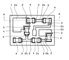
- FIG. 1 to 4 show a circuit board according to a first embodiment of the present invention.
- 1 to 3 are exploded plan views
- FIG. 4 is a schematic cross-sectional view taken along the chain line AA in FIG. 3, and
- FIG. 1 is obtained by removing the resin layer, chip parts, and line resist pattern from the circuit board.
- FIG. 2 shows a state where the resin layer and the chip component are removed
- FIG. 3 shows a state where the resin layer is removed.
- 1 is a core substrate.
- An electrode pattern 2 made of a metal film is formed on the first main surface (upper surface) of the core substrate 1.
- a glass epoxy substrate is used as the core substrate 1
- a copper foil film is used as the electrode film of the electrode pattern 2.
- the electrode pattern 2 is divided into a mounting electrode pattern 2a, a connection electrode pattern 2b, a capacitor electrode pattern 2c, and a ground electrode pattern 2d.
- the mounting electrode pattern 2a is for joining terminal electrodes of chip components to be mounted with, for example, a conductive member such as solder.
- connection electrode pattern 2b is for connecting between the mounting electrode patterns 2a or between the mounting electrode pattern 2a and the capacitor electrode pattern 2c.
- the capacitor electrode pattern 2c constitutes one electrode of a capacitor (not shown) formed on the circuit board using the core substrate 1 itself as a dielectric.
- the other electrode of the capacitor is formed inside the core substrate 1 or on the second main surface of the core substrate 1.
- the ground electrode pattern 2d is used as a ground electrode of this circuit board.
- the mounting electrode pattern 2a and the other part of the electrode pattern 2 are partitioned by a line resist pattern 3 made of a material that hinders adhesion of molten solder.
- a line resist pattern 3 made of a material that hinders adhesion of molten solder.
- an epoxy resin is used as the material of the line resist pattern 3, and the line width can be set to 150 ⁇ m, for example.
- the terminal electrodes of the chip component 4 are joined to the mounting electrode pattern 2a of the core substrate 1 by solder (not shown).
- a resin layer 5 is further formed on the core substrate 1 on which the chip component 4 is mounted.
- a thermosetting epoxy resin can be used for the resin layer 5.
- the circuit board according to the first embodiment of the present invention having the above structure is provided with the line-shaped resist pattern 3 between the electrode pattern 2 and the resin layer 5 to the minimum necessary, A large bonding area between the high-strength electrode pattern 2 and the resin layer 5 can be secured, and as a result, the adhesion strength between the core substrate 1 and the resin layer 5 is large. Further, since the line resist pattern 3 becomes an anchor for the resin layer 5, the adhesion strength between the core substrate 1 and the resin layer 5 is further increased. Further, when the terminal electrode of the chip component 4 is soldered to the mounting electrode pattern 2a, the line-shaped resist pattern 3 surely prevents the molten solder from flowing out from the mounting electrode pattern 2a to the electrode pattern 2. Has been prevented.
- the electrode pattern 2 and the chip component 4 are protected from the outside by the resin layer 5, and the moisture resistance and rust resistance are also improved. Furthermore, compared with the conventional example shown in FIG. 9, the exposure of the electrode pattern is increased, and thus the ratio of the stepped portion between the core substrate 1 and the electrode pattern is increased. This stepped portion contributes to the anchor effect, and the resin layer The adhesion strength to the core substrate 1 is further increased.
- FIGS. 1 to 4 are appropriately referred to.
- an electrode pattern 2 having a desired shape is formed on a first main surface of a core substrate 1 having a copper foil attached to the entire surface by a subtractive method (photolithography and etching). .
- a resist ink is printed or applied on the surface of the core substrate 1 and dried, patterned exposure, developed, and cured to form a line resist on a desired portion on the electrode pattern 2 as shown in FIG. Pattern 3 is formed.
- solder paste is applied on the mounting electrode pattern 2a, and the terminal electrode of the chip component 4 is mounted thereon, heated and cooled, and the solder is solidified. As shown in FIG. 4 terminal electrodes are joined to the mounting electrode pattern 2a.
- thermosetting epoxy resin that is heated and made into a semi-molten state is disposed on the core substrate 1 on which the chip component 4 is mounted, and further heated to form a thermosetting epoxy resin. Is cured, the resin layer 5 is formed, and the circuit board according to the first embodiment is completed.
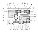
- FIG. 5 to 7 show a circuit board according to a second embodiment of the present invention.
- 5 and 6 are exploded plan views
- FIG. 7 is a schematic cross-sectional view taken along the chain line BB in FIG. 6,
- FIG. 5 shows a state where the resin layer and chip parts are removed from the circuit board, and
- FIG. The state which removed the resin layer is shown.
- regions of the electrode pattern 2 other than the mounting electrode pattern 2a that is, the surfaces of the connection electrode pattern 2b, the capacitor electrode pattern 2c, and the ground electrode pattern 2d are roughened. This is different from the first embodiment.
- the circuit board according to the second embodiment has a roughened connection electrode pattern 2b ′, a roughened capacitor electrode pattern 2c ′, and a roughened surface, as shown in FIGS.
- a ground electrode pattern 2d ' is provided.
- the surface roughness of these electrode patterns is larger than the surface roughness of the mounting electrode pattern 2a. Moreover, it is larger than the surface roughness of the first main surface of the core substrate 1.
- the circuit board according to the second embodiment includes a roughened connection electrode pattern 2b ′, a roughened capacitor electrode pattern 2c ′, a roughened ground electrode pattern 2d ′, and a resin layer. Since the adhesive strength between the core substrate 1 and the resin layer 5 is higher than that of the first embodiment, the adhesive strength between the core substrate 1 and the resin layer 5 is higher than that of the first embodiment.
- the electrode pattern 2a for mounting is masked, and exposed to a roughening solution formed by mixing sulfuric acid and hydrogen peroxide or a roughening solution containing a persulfate, for example, to expose the electrode pattern.
- a roughened connection electrode pattern 2b ′, a roughened capacitor electrode pattern 2c ′, and a roughened ground electrode pattern 2d ′ are formed.
- a method such as sandblasting may be used regardless of chemicals.
- circuit board according to the second embodiment is completed using the same method as the manufacturing method of the first embodiment.
- circuit board according to the first and second embodiments of the present invention and an example of the manufacturing method thereof have been described above.
- the present invention is not limited to these contents, and various modifications can be made.
- the core substrate 1 is not limited to a glass epoxy substrate, and other materials such as a ceramic substrate can be used.
- the core substrate 1 is not limited to a single layer structure, and a multilayer structure in which electrodes are formed and components are incorporated can also be used.
- the metal film forming the electrode pattern 2 is not limited to copper, and other materials such as silver can be used.
- the electrode pattern partitioned from the electrode pattern 2 is not limited to the mounting electrode pattern 2a, the connection electrode pattern 2b, the capacitor electrode pattern 2c, and the ground electrode pattern 2d, but may be an electrode pattern that performs other functions.
- the line resist pattern 3 is not limited to the epoxy resin, and other materials can be used.
- the line width of the line resist pattern 3 is also arbitrary and is not limited to 150 ⁇ m.
- the electrode pattern 2 is not covered with a resist pattern, and when the chip component 4 is mounted on the mounting electrode pattern 12a, the molten solder flows out onto the electrode pattern 12 following the mounting electrode pattern 12a. In order to dampen this, it is preferably about 50 to 300 ⁇ m.
- the line-shaped resist pattern 3 is not only between the mounting electrode pattern 2a and the connection electrode pattern 2b and between the mounting electrode pattern 2a and the ground electrode pattern 2d, but also between the mounting electrode patterns 2a. Alternatively, it may be formed between the mounting electrode pattern 2a and the capacitor electrode pattern 2c.
- the resin layer 5 is not limited to the thermosetting epoxy resin, and other materials can be used.
- Electrode pattern 2a Mounting electrode pattern 2b: Connection electrode pattern 2c: Capacitor electrode pattern 2d: Ground electrode pattern 2b ′: Roughened connection electrode pattern 2c ′: Roughened capacitor electrode Pattern 2d ': Roughened ground electrode pattern 3: Line resist pattern 4: Chip component 5: Resin layer
Landscapes
- Engineering & Computer Science (AREA)
- Manufacturing & Machinery (AREA)
- Microelectronics & Electronic Packaging (AREA)
- Non-Metallic Protective Coatings For Printed Circuits (AREA)
- Production Of Multi-Layered Print Wiring Board (AREA)
- Electric Connection Of Electric Components To Printed Circuits (AREA)
- Structure Of Printed Boards (AREA)
Abstract
電極パターンが形成されたコア基板上にチップ部品を実装し、さらにその上に樹脂層を設けてなる回路基板において、コア基板と樹脂層との密着強度の向上をはかる。 コア基板の第1主面に、実装用電極パターンを含む大面積の電極パターンを形成し、実装用電極パターンを、電極パターンの一部をライン状レジストパターンで区画して形成するようにした。
Description
本発明は、電極パターンが形成されたコア基板上にチップ部品を実装し、さらにその上に樹脂層を設けてなる回路基板に関し、さらに詳しくは、コア基板と樹脂層との密着強度の向上をはかった回路基板に関する。
コア基板上に所望の電極パターンを設け、その電極パターン上にチップ部品を実装してなる回路基板においては、例えば特許文献1(特開平9-148722号公報)に開示されるように、コア基板上に形成した電極パターンのうち、チップ部品の端子電極がはんだ付けされる実装用電極パターン以外の領域を、レジストパターンで覆うことが多い。
図8~図11に、そのような構造からなる従来の回路基板を示す。なお、図8、図9は分解平面図、図10は平面図、図11は図10の鎖線C-C部分の断面模式図であり、図8はこの回路基板からチップ部品とレジストパターンを取り除いた状態、図9はチップ部品を取り除いた状態を示す。
図8において、11はコア基板であり、ガラス繊維にエポキシ樹脂を含浸したプリント基板などからなる。コア基板11の第1主面(上面)には、銅などの金属膜からなる電極パターン12が形成されている。電極パターン12は、例えば、コア基板11の第1主面の全面に金属箔を貼り、これをエッチングすることにより形成される。なお、電極パターン12は、その機能により、チップ電極の端子電極がはんだ付けされる実装用電極パターン、接続電極パターン、グランド電極パターンなどに区画される。
そして、図9に示すように、電極パターン12のうち、チップ部品の端子電極がはんだ付けされる実装用電極パターン12a以外の領域上に、所望の形状からなる、レジストパターン13が形成されている。レジストパターン13は、例えば、所望の形状にレジストインクを塗布し、乾燥、現像することにより形成される。
そして、図10、図11に示すように、実装用電極パターン12a上には、チップ部品14の端子電極が、はんだ(図示せず)により接合されている。チップ部品14の端子電極の実装用電極パターン12aへの接合は、例えば、実装用電極パターン12a上にはんだペーストを塗布しておき、その上に端子電極が実装用電極パターン12aに位置するようにチップ部品14を実装し、加熱、冷却することによりおこなわれる。
このような回路基板において、電極パターン12のうち、実装用電極パターン12a以外の領域をレジストパターン13で覆うのは、チップ部品14を実装用電極パターン12a上に実装する際に、溶融したはんだが流出し、電極パターン12上を流れてゆくのを堰き止めるとともに、電極パターン12のうち、実装用電極パターン12a以外の領域を外部から保護し、耐湿性や防錆性を向上させることなどが目的である。
近時、上述したような回路基板において、チップ部品を実装したコア基板上に、さらに樹脂層を設けることがおこなわれている。
図12に、図10、図11に示した従来の回路基板上に、さらに樹脂層を設けた回路基板を示す。なお、図12は、図10の鎖線C-C部分に対応する部分を示した断面模式図である。
図12に示すように、この回路基板においては、電極パターン12、ソルダーレジスト13が形成され、チップ部品14が実装されたコア基板11の上に、さらに樹脂層15が形成されている。この樹脂層15は、チップ部品14を外部から保護する機能や、回路基板全体の強度を向上させる機能をはたす。
しかしながら、この回路基板には、コア基板11と樹脂層15との密着強度が小さいという問題がある。これは、電極パターン12のうち、実装用電極パターン12a以外の領域が、レジストパターン13により覆われているためである。 すなわち、一般に、レジストパターン13の表面は平滑であるため、電極パターン12を構成する金属膜に比べて、樹脂層15に対するアンカー力が小さく、樹脂層15との密着強度が小さくなってしまうためである。そのため、この回路基板を別の大きな回路基板に実装するような場合に、この回路基板が吸湿状態であると、密着強度の小さいレジストパターン13と樹脂層15との界面においてデラミネーションが発生してしまう恐れがあった。
本発明は、上述した従来の回路基板の問題点を解決するためになされたものであり、その手段として本発明の回路基板は、コア基板と、コア基板の第1主面に設けられた、チップ部品を実装するための実装用電極パターンと、実装用電極パターンにはんだを介して実装されたチップ部品と、チップ部品を覆うようにコア基板の第1主面上に設けられた樹脂層とを有する回路基板において、コア基板の第1主面に、実装用電極パターンを含む電極パターンを形成し、実装用電極パターンを、電極パターンの一部をライン状レジストパターンで区画することによって形成するようにした。
なお、電極パターンのうち、実装用電極パターンに区画されなかった領域の表面粗さを、実装用電極パターンの表面粗さよりも大きくすると、樹脂層との密着強度をより大きくすることができるため好ましい。
また、電極パターンのうち、実装用電極パターンに区画されなかった領域の表面粗さを、コア基板の第1主面の表面粗さよりも大きくすると、樹脂層との密着強度をより大きくできるため好ましい。
このような構成からなる本発明の回路基板は、電極パターンと樹脂層との間には、必要最小限のライン状のレジストパターンしか介在しておらず、電極パターンと樹脂層との接合面積が大きいため、コア基板と樹脂層との密着強度が大きい。この結果、この回路基板を別の大きな回路基板に実装するような場合に、たとえ、この回路基板が吸湿状態であったとしても、コア基板と樹脂層との界面においてデラミネーションが発生することがない。
以下、図面を参照しつつ、本発明を実施するための形態について説明する。
[第1の実施形態]
図1~図4に、本発明の第1の実施形態にかかる回路基板を示す。なお、図1~図3は分解平面図、図4は図3の鎖線A-A部分の断面模式図であり、図1はこの回路基板から樹脂層とチップ部品とライン状レジストパターンを取り除いた状態、図2は樹脂層とチップ部品を取り除いた状態、図3は樹脂層を取り除いた状態を示す。
図1~図4に、本発明の第1の実施形態にかかる回路基板を示す。なお、図1~図3は分解平面図、図4は図3の鎖線A-A部分の断面模式図であり、図1はこの回路基板から樹脂層とチップ部品とライン状レジストパターンを取り除いた状態、図2は樹脂層とチップ部品を取り除いた状態、図3は樹脂層を取り除いた状態を示す。
図1において、1はコア基板である。コア基板1の第1主面(上面)には、金属膜からなる電極パターン2が形成されている。本実施形態においては、コア基板1としてガラスエポキシ基板、電極パターン2の電極膜として銅箔膜を用いた。
電極パターン2は、図2に示すように、実装用電極パターン2a、接続電極パターン2b、コンデンサ電極パターン2c、グランド電極パターン2dに区画されている。
実装用電極パターン2aは、実装されるチップ部品の端子電極を、たとえば、はんだ等の導電部材で接合するためのものである。
接続電極パターン2bは、実装用電極パターン2aどうしの間、あるいは実装用電極パターン2aとコンデンサ電極パターン2cとの間などを接続するためのものである。
コンデンサ電極パターン2cは、コア基板1自体を誘電体としてこの回路基板に形成されたコンデンサ(図示せず)の一方の電極を構成するものである。なお、コンデンサの他方の電極は、コア基板1の内部、あるいはコア基板1の第2主面に形成されている。
グランド電極パターン2dは、この回路基板のグランド電極として用いられるものである。
実装用電極パターン2aと、電極パターン2の他の部分との間は、溶融したはんだが付着するのを阻害する材質からなる、ライン状レジストパターン3により区画されている。本実施形態においては、ライン状レジストパターン3の材質として、例えば、エポキシ樹脂を用い、例えば、ライン幅は150μmとすることができる。
そして、図3に示すように、コア基板1の実装用電極パターン2a上に、チップ部品4の端子電極が、はんだ(図示せず)により接合されている。
そして、図4に示すように、チップ部品4が実装されたコア基板1上には、さらに樹脂層5が形成されている。例えば、樹脂層5に熱硬化型エポキシ樹脂を用いることができる。
以上の構造からなる、本発明の第1の実施形態にかかる回路基板は、電極パターン2と樹脂層5との間に、必要最小限にしかライン状レジストパターン3が設けられていないため、密着強度の高い電極パターン2と樹脂層5との接合面積を大きく確保することができ、ひいてはコア基板1と樹脂層5との密着強度が大きい。また、ライン状レジストパターン3が樹脂層5に対するアンカーとなるため、コア基板1と樹脂層5の密着強度はさらに大きくなる。また、実装用電極パターン2aにチップ部品4の端子電極をはんだ付けする際の、溶融したはんだの実装用電極パターン2aから、これに続く電極パターン2への流出は、ライン状レジストパターン3により確実に防止されている。さらに、電極パターン2やチップ部品4は、樹脂層5により外部から保護され、耐湿性や防錆性も向上している。さらに、図9に示した従来例に比べて、電極パターンの露出が多くなり、よって、コア基板1と電極パターンの段差部分の割合が増えるため、この段差部分がアンカー効果に寄与し、樹脂層5のコア基板1への密着強度がさらに大きくなる。
次に、本発明の第1の実施形態にかかる回路基板の製造方法の一例について説明する。なお、説明においては、図1~4を適宜参照する。
まず、全面に銅箔が貼りつけられたコア基板1の第1主面に、サブトラクティブ法(フォトリソグラフィーおよびエッチング)により、図1に示すように、所望の形状からなる電極パターン2を形成する。
次に、コア基板1の表面にレジストインクを印刷、あるいは塗布し、乾燥、パターン露光、現像、硬化することにより、図2に示すように、電極パターン2上の所望の部分に、ライン状レジストパターン3を形成する。
次に、実装用電極パターン2a上に、はんだペーストを塗布し、その上にチップ部品4の端子電極を実装し、加熱、冷却し、はんだを固化させて、図3に示すように、チップ部品4の端子電極を実装用電極パターン2aに接合する。
最後に、図4に示すように、チップ部品4が実装されたコア基板1上に、加熱されて半溶融状になった熱硬化型エポキシ樹脂を配置し、さらに加熱して熱硬化型エポキシ樹脂を硬化させ、樹脂層5を形成し、第1の実施形態にかかる回路基板を完成させる。
[第2の実施形態]
図5~図7に、本発明の第2の実施形態にかかる回路基板を示す。なお、図5、図6は分解平面図、図7は図6の鎖線B-B部分の断面模式図であり、図5はこの回路基板から樹脂層とチップ部品を取り除いた状態、図6は樹脂層を取り除いた状態を示す。
図5~図7に、本発明の第2の実施形態にかかる回路基板を示す。なお、図5、図6は分解平面図、図7は図6の鎖線B-B部分の断面模式図であり、図5はこの回路基板から樹脂層とチップ部品を取り除いた状態、図6は樹脂層を取り除いた状態を示す。
第2の実施形態にかかる回路基板は、電極パターン2のうち、実装用電極パターン2a以外の領域、すなわち、接続電極パターン2b、コンデンサ電極パターン2c、グランド電極パターン2dの表面が、粗面化されていることが、第1の実施形態と異なる。
すなわち、第2の実施形態にかかる回路基板は、図5~図7に示すように、粗面化された接続電極パターン2b’、粗面化されたコンデンサ電極パターン2c’、粗面化されたグランド電極パターン2d’を有している。これらの電極パターンの表面粗さは、実装用電極パターン2aの表面粗さよりも大きい。また、コア基板1の第1主面の表面粗さよりも大きい。
この結果、第2の実施形態にかかる回路基板は、粗面化された接続電極パターン2b’、粗面化されたコンデンサ電極パターン2c’、粗面化されたグランド電極パターン2d’と、樹脂層5との接着強度が第1の実施形態よりも大きくなっているため、コア基板1と樹脂層5との接着強度が第1の実施形態よりも大きくなっている。
次に、第2の実施形態にかかる回路基板の製造方法の一例について説明する。
この製造方法においては、電極パターン2上にライン状レジストパターン3を形成するところまでは、上述した第1の実施形態の製造方法と同じ方法を用いる(図2参照)。
次に、実装用電極パターン2aをマスキングし、例えば、硫酸と過酸化水素とを混合してなる粗化処理液、あるいは過硫酸塩を含む粗化処理液に浸漬することにより、露出した電極パターンを酸化させて、図5に示すように、粗面化された接続電極パターン2b’、粗面化されたコンデンサ電極パターン2c’、粗面化されたグランド電極パターン2d’を形成する。なお、粗面化は、薬品によらず、サンドブラストなどの方法を用いても良い。
この後、第1の実施形態の製造方法と同じ方法を用いて、第2の実施形態にかかる回路基板を完成させる。
以上、本発明の第1、第2の実施形態にかかる回路基板、およびそれらの製造方法の一例について説明した。しかしながら、本発明がこれらの内容に限定されることはなく、種々の変更をなすことができる。
例えば、コア基板1はガラスエポキシ基板に限られず、セラミック基板など、他の材質のものを用いることができる。また、コア基板1は単層構造のものに限られず、内部に電極が形成され、さらに部品が内蔵された多層構造のものを用いることもできる。
また、電極パターン2を形成する金属膜も銅に限られず、銀など、他の材質のものを用いることができる。そして、電極パターン2から区画される電極パターンも、実装用電極パターン2a、接続電極パターン2b、コンデンサ電極パターン2c、グランド電極パターン2dに限られず、他の機能をはたす電極パターンであっても良い。
また、ライン状レジストパターン3もエポキシ樹脂に限られず、他の材質のものを用いることができる。そして、ライン状レジストパターン3のライン幅も任意であり、150μmには限られない。ただし、できる限り電極パターン2上をレジストパターンで覆わず、かつチップ部品4を実装用電極パターン12a上に実装する際に、溶融したはんだが、実装用電極パターン12aに続く電極パターン12上に流出するのを堰き止めるためには、50~300μm程度が好ましい。また、ライン状レジストパターン3は、実装用電極パターン2aと接続電極パターン2bとの間、および実装用電極パターン2aとグランド電極パターン2dとの間のみならず、実装用電極パターン2aどうしの間や、実装用電極パターン2aとコンデンサ電極パターン2cとの間に形成するようにしても良い。
さらに、樹脂層5も熱硬化性エポキシ樹脂に限られず、他の材質のものを用いることができる。
1:コア基板
2:電極パターン
2a:実装用電極パターン
2b:接続電極パターン
2c:コンデンサ電極パターン
2d:グランド電極パターン
2b’:粗面化された接続電極パターン
2c’:粗面化されたコンデンサ電極パターン
2d’:粗面化されたグランド電極パターン
3:ライン状レジストパターン
4:チップ部品
5:樹脂層
2:電極パターン
2a:実装用電極パターン
2b:接続電極パターン
2c:コンデンサ電極パターン
2d:グランド電極パターン
2b’:粗面化された接続電極パターン
2c’:粗面化されたコンデンサ電極パターン
2d’:粗面化されたグランド電極パターン
3:ライン状レジストパターン
4:チップ部品
5:樹脂層
Claims (4)
- コア基板と、前記コア基板の第1主面に設けられた、チップ部品を実装するための実装用電極パターンと、前記実装用電極パターンにはんだを介して実装されたチップ部品と、前記チップ部品を覆うように前記コア基板の前記第1主面上に設けられた樹脂層と、を有する回路基板において、
前記コア基板の前記第1主面には、前記実装用電極パターンを含む電極パターンが形成され、前記実装用電極パターンが、前記電極パターンの一部をライン状レジストパターンで区画することによって形成されていることを特徴とする回路基板。 - 前記電極パターンのうち、前記実装用電極パターンに区画されなかった領域の表面粗さが、前記実装用電極パターンの表面粗さよりも大きいことを特徴とする、請求項1に記載された回路基板。
- 前記電極パターンのうち、前記実装用電極パターンに区画されなかった領域の表面粗さが、前記コア基板の前記第1主面の表面粗さよりも大きいことを特徴とする、請求項1または2に記載された回路基板。
- 前記コア基板の前記第1主面には、前記実装用電極パターンが複数個設けられており、前記実装用電極パターンは、前記電極パターンの一部を区画して形成された接続電極パターンによって互いに接続されており、かつ、前記実装用電極パターンと前記接続電極パターンとが、ライン状レジストパターンによって区画されていることを特徴とする、請求項1ないし3のいずれか1項に記載された回路基板。
Priority Applications (1)
| Application Number | Priority Date | Filing Date | Title |
|---|---|---|---|
| JP2011534280A JPWO2011040480A1 (ja) | 2009-09-30 | 2010-09-29 | 回路基板 |
Applications Claiming Priority (2)
| Application Number | Priority Date | Filing Date | Title |
|---|---|---|---|
| JP2009226848 | 2009-09-30 | ||
| JP2009-226848 | 2009-09-30 |
Publications (1)
| Publication Number | Publication Date |
|---|---|
| WO2011040480A1 true WO2011040480A1 (ja) | 2011-04-07 |
Family
ID=43826294
Family Applications (1)
| Application Number | Title | Priority Date | Filing Date |
|---|---|---|---|
| PCT/JP2010/066972 WO2011040480A1 (ja) | 2009-09-30 | 2010-09-29 | 回路基板 |
Country Status (2)
| Country | Link |
|---|---|
| JP (1) | JPWO2011040480A1 (ja) |
| WO (1) | WO2011040480A1 (ja) |
Cited By (1)
| Publication number | Priority date | Publication date | Assignee | Title |
|---|---|---|---|---|
| WO2022113639A1 (ja) * | 2020-11-26 | 2022-06-02 | 日本電産サーボ株式会社 | 基板、モータ、及び軸流ファン |
Citations (3)
| Publication number | Priority date | Publication date | Assignee | Title |
|---|---|---|---|---|
| JPS6310582U (ja) * | 1986-07-09 | 1988-01-23 | ||
| JP2002324968A (ja) * | 2001-04-24 | 2002-11-08 | Ngk Spark Plug Co Ltd | 配線基板の製造方法 |
| JP2004235403A (ja) * | 2003-01-30 | 2004-08-19 | Matsushita Electric Ind Co Ltd | 複合電子部品 |
Family Cites Families (4)
| Publication number | Priority date | Publication date | Assignee | Title |
|---|---|---|---|---|
| JPH0611531Y2 (ja) * | 1988-07-30 | 1994-03-23 | 太陽誘電株式会社 | 回路基板装置 |
| JPH04206683A (ja) * | 1990-11-30 | 1992-07-28 | Mitsuba Electric Mfg Co Ltd | 配線基板の製造方法 |
| JP2005183430A (ja) * | 2003-12-16 | 2005-07-07 | Matsushita Electric Ind Co Ltd | 電子部品内蔵モジュール |
| JP5172275B2 (ja) * | 2007-10-26 | 2013-03-27 | パナソニック株式会社 | 部品内蔵プリント配線基板および部品内蔵プリント配線基板の製造方法 |
-
2010
- 2010-09-29 WO PCT/JP2010/066972 patent/WO2011040480A1/ja active Application Filing
- 2010-09-29 JP JP2011534280A patent/JPWO2011040480A1/ja active Pending
Patent Citations (3)
| Publication number | Priority date | Publication date | Assignee | Title |
|---|---|---|---|---|
| JPS6310582U (ja) * | 1986-07-09 | 1988-01-23 | ||
| JP2002324968A (ja) * | 2001-04-24 | 2002-11-08 | Ngk Spark Plug Co Ltd | 配線基板の製造方法 |
| JP2004235403A (ja) * | 2003-01-30 | 2004-08-19 | Matsushita Electric Ind Co Ltd | 複合電子部品 |
Cited By (1)
| Publication number | Priority date | Publication date | Assignee | Title |
|---|---|---|---|---|
| WO2022113639A1 (ja) * | 2020-11-26 | 2022-06-02 | 日本電産サーボ株式会社 | 基板、モータ、及び軸流ファン |
Also Published As
| Publication number | Publication date |
|---|---|
| JPWO2011040480A1 (ja) | 2013-02-28 |
Similar Documents
| Publication | Publication Date | Title |
|---|---|---|
| KR102212827B1 (ko) | 인쇄회로기판, 패키지 기판 및 이의 제조 방법 | |
| US8418358B2 (en) | Wiring board with built-in component and method for manufacturing wiring board with built-in component | |
| US6740352B2 (en) | Method for forming bonding pads | |
| JP7074409B2 (ja) | 素子内蔵型印刷回路基板 | |
| US20080251280A1 (en) | Soldering structure between circuit boards | |
| JP2006140327A (ja) | 配線基板およびこれを用いた電子部品の実装方法 | |
| JP5172275B2 (ja) | 部品内蔵プリント配線基板および部品内蔵プリント配線基板の製造方法 | |
| JP5354224B2 (ja) | 部品内蔵モジュールの製造方法 | |
| TWI586232B (zh) | 印刷電路板及其製造方法 | |
| JP2009147026A (ja) | 回路基板およびその製造方法 | |
| WO2011040480A1 (ja) | 回路基板 | |
| JP2007059588A (ja) | 配線基板の製造方法および配線基板 | |
| JP2012164934A (ja) | 回路モジュール、電子部品実装基板および回路モジュールの製造方法 | |
| JP2004327743A (ja) | 半田バンプ付き配線基板およびその製造方法 | |
| JP6570728B2 (ja) | 電子装置およびその製造方法 | |
| JP2011135111A (ja) | プリント配線板のフレームグランド形成方法 | |
| JP2013219284A (ja) | 電子部品実装基板の製造方法 | |
| JP6623056B2 (ja) | 配線基板、半導体装置 | |
| JP7366578B2 (ja) | 電子モジュール及び電子機器 | |
| KR20080071431A (ko) | 반도체 모듈 및 이의 베어 다이 실장 방법 | |
| JP2005032943A (ja) | 表面実装素子用基板 | |
| JP3037320B1 (ja) | プリント配線基板の部品実装構造 | |
| JP2021072423A (ja) | 配線板及びその製造方法 | |
| JP2007180078A (ja) | プリント基板 | |
| WO2011093068A1 (ja) | 部品内蔵基板の製造方法および部品内蔵基板 |
Legal Events
| Date | Code | Title | Description |
|---|---|---|---|
| 121 | Ep: the epo has been informed by wipo that ep was designated in this application |
Ref document number: 10820595 Country of ref document: EP Kind code of ref document: A1 |
|
| WWE | Wipo information: entry into national phase |
Ref document number: 2011534280 Country of ref document: JP |
|
| NENP | Non-entry into the national phase |
Ref country code: DE |
|
| 122 | Ep: pct application non-entry in european phase |
Ref document number: 10820595 Country of ref document: EP Kind code of ref document: A1 |