WO2011040102A1 - 色素増感型太陽電池 - Google Patents
色素増感型太陽電池 Download PDFInfo
- Publication number
- WO2011040102A1 WO2011040102A1 PCT/JP2010/061487 JP2010061487W WO2011040102A1 WO 2011040102 A1 WO2011040102 A1 WO 2011040102A1 JP 2010061487 W JP2010061487 W JP 2010061487W WO 2011040102 A1 WO2011040102 A1 WO 2011040102A1
- Authority
- WO
- WIPO (PCT)
- Prior art keywords
- dye
- layer
- solar cell
- sensitized solar
- substrate
- Prior art date
- Legal status (The legal status is an assumption and is not a legal conclusion. Google has not performed a legal analysis and makes no representation as to the accuracy of the status listed.)
- Ceased
Links
Images


Classifications
-
- H—ELECTRICITY
- H01—ELECTRIC ELEMENTS
- H01G—CAPACITORS; CAPACITORS, RECTIFIERS, DETECTORS, SWITCHING DEVICES, LIGHT-SENSITIVE OR TEMPERATURE-SENSITIVE DEVICES OF THE ELECTROLYTIC TYPE
- H01G9/00—Electrolytic capacitors, rectifiers, detectors, switching devices, light-sensitive or temperature-sensitive devices; Processes of their manufacture
- H01G9/20—Light-sensitive devices
- H01G9/2068—Panels or arrays of photoelectrochemical cells, e.g. photovoltaic modules based on photoelectrochemical cells
- H01G9/2077—Sealing arrangements, e.g. to prevent the leakage of the electrolyte
-
- H—ELECTRICITY
- H01—ELECTRIC ELEMENTS
- H01G—CAPACITORS; CAPACITORS, RECTIFIERS, DETECTORS, SWITCHING DEVICES, LIGHT-SENSITIVE OR TEMPERATURE-SENSITIVE DEVICES OF THE ELECTROLYTIC TYPE
- H01G9/00—Electrolytic capacitors, rectifiers, detectors, switching devices, light-sensitive or temperature-sensitive devices; Processes of their manufacture
- H01G9/20—Light-sensitive devices
- H01G9/2068—Panels or arrays of photoelectrochemical cells, e.g. photovoltaic modules based on photoelectrochemical cells
- H01G9/2081—Serial interconnection of cells
-
- H—ELECTRICITY
- H01—ELECTRIC ELEMENTS
- H01G—CAPACITORS; CAPACITORS, RECTIFIERS, DETECTORS, SWITCHING DEVICES, LIGHT-SENSITIVE OR TEMPERATURE-SENSITIVE DEVICES OF THE ELECTROLYTIC TYPE
- H01G9/00—Electrolytic capacitors, rectifiers, detectors, switching devices, light-sensitive or temperature-sensitive devices; Processes of their manufacture
- H01G9/20—Light-sensitive devices
- H01G9/2027—Light-sensitive devices comprising an oxide semiconductor electrode
- H01G9/2031—Light-sensitive devices comprising an oxide semiconductor electrode comprising titanium oxide, e.g. TiO2
-
- H—ELECTRICITY
- H01—ELECTRIC ELEMENTS
- H01G—CAPACITORS; CAPACITORS, RECTIFIERS, DETECTORS, SWITCHING DEVICES, LIGHT-SENSITIVE OR TEMPERATURE-SENSITIVE DEVICES OF THE ELECTROLYTIC TYPE
- H01G9/00—Electrolytic capacitors, rectifiers, detectors, switching devices, light-sensitive or temperature-sensitive devices; Processes of their manufacture
- H01G9/20—Light-sensitive devices
- H01G9/2059—Light-sensitive devices comprising an organic dye as the active light absorbing material, e.g. adsorbed on an electrode or dissolved in solution
-
- H—ELECTRICITY
- H01—ELECTRIC ELEMENTS
- H01G—CAPACITORS; CAPACITORS, RECTIFIERS, DETECTORS, SWITCHING DEVICES, LIGHT-SENSITIVE OR TEMPERATURE-SENSITIVE DEVICES OF THE ELECTROLYTIC TYPE
- H01G9/00—Electrolytic capacitors, rectifiers, detectors, switching devices, light-sensitive or temperature-sensitive devices; Processes of their manufacture
- H01G9/20—Light-sensitive devices
- H01G9/2095—Light-sensitive devices comprising a flexible sustrate
-
- H—ELECTRICITY
- H10—SEMICONDUCTOR DEVICES; ELECTRIC SOLID-STATE DEVICES NOT OTHERWISE PROVIDED FOR
- H10K—ORGANIC ELECTRIC SOLID-STATE DEVICES
- H10K2102/00—Constructional details relating to the organic devices covered by this subclass
- H10K2102/10—Transparent electrodes, e.g. using graphene
- H10K2102/101—Transparent electrodes, e.g. using graphene comprising transparent conductive oxides [TCO]
- H10K2102/103—Transparent electrodes, e.g. using graphene comprising transparent conductive oxides [TCO] comprising indium oxides, e.g. ITO
-
- Y—GENERAL TAGGING OF NEW TECHNOLOGICAL DEVELOPMENTS; GENERAL TAGGING OF CROSS-SECTIONAL TECHNOLOGIES SPANNING OVER SEVERAL SECTIONS OF THE IPC; TECHNICAL SUBJECTS COVERED BY FORMER USPC CROSS-REFERENCE ART COLLECTIONS [XRACs] AND DIGESTS
- Y02—TECHNOLOGIES OR APPLICATIONS FOR MITIGATION OR ADAPTATION AGAINST CLIMATE CHANGE
- Y02E—REDUCTION OF GREENHOUSE GAS [GHG] EMISSIONS, RELATED TO ENERGY GENERATION, TRANSMISSION OR DISTRIBUTION
- Y02E10/00—Energy generation through renewable energy sources
- Y02E10/50—Photovoltaic [PV] energy
- Y02E10/542—Dye sensitized solar cells
Definitions
- the present invention relates to a dye-sensitized solar cell.
- a general dye-sensitized solar cell 100 includes a base 110 for a dye-sensitized solar cell in which a first electrode layer 112 is laminated on a base 111, A structure in which a porous layer 102 containing metal oxide semiconductor fine particles carrying a dye sensitizer and an electrolyte layer 101 are formed inside a sealing material 103 between a counter electrode substrate 120 having a function as an electrode. It is what you have.
- the dye sensitizer adsorbed on the surface of the metal oxide semiconductor fine particles in the porous layer 102 is excited by receiving sunlight from the substrate 111 side, and the excited electrons are conducted to the first electrode layer. , And conducted to the counter electrode substrate through an external circuit. Thereafter, electricity is generated by returning the electrons to the ground level of the dye sensitizer through the redox pair.
- a typical example of such a dye-sensitized solar cell is a Gretcher cell in which the porous layer is made of porous titanium dioxide and the content of the dye sensitizer is increased. It has been widely studied as a sensitized solar cell.
- a so-called 'inverted structure cell type' configuration in which the porous layer 102 is formed in contact with the counter electrode substrate 120 side. There are also known.
- reverse electron transfer means a phenomenon in which electrons flow from the electrode to the electrolyte layer.
- reverse electron transfer is a phenomenon in which electrons flow from the first electrode layer 112 to the electrolyte layer 101, and FIG. Taking the dye-sensitized solar cell exemplified in b) as an example, it means a phenomenon in which electrons flow from the counter electrode substrate 120 to the electrolyte layer 101.
- the base material on which the first electrode layer is laminated, or the first electrode layer and The base material on which the porous layer is laminated is immersed in a titanium tetrachloride solution or a titanium tetraisopropoxide solution to form a dense titanium oxide layer on the surface of the first electrode layer and the porous layer.
- a method for preventing contact with an electrode layer is known (for example, Patent Documents 1 and 2).
- a method of forming a porous layer so as to cover the surface of the first electrode layer is also known (for example, Patent Document 3).
- JP 2007-157397 A (for example, paragraph [0046]) JP 2007-073346 A (for example, [0033] paragraph) JP 2006-19072 A
- the dye-sensitized solar cell illustrated in FIG. 7A will be described as an example. Reverse electron transfer occurs where the electrolyte layer and the first electrode layer are in contact with each other, so that the dye-sensitized solar cell having a normal structure is used. In the battery, the first electrode layer and the electrolyte layer are in contact with each other at the interface between the porous layer and the first electrode layer in which the electrolyte layer indirectly contacts the first electrode layer via the porous layer (FIG. 7A).
- the interface indicated by A), and the interface between the electrolyte layer and the first electrode layer (the interface indicated by B in FIG. 7A) in which the electrolyte layer and the first electrode layer are in direct contact with each other. was revealed. And when comparing the area of those interfaces, the former interface is overwhelmingly larger in area than the latter interface, so it is efficient to reduce the former interface to prevent reverse electron transfer. Predicted. However, as a result of further investigation by the present inventors, the interface between the electrolyte layer and the first electrode layer has a very small area compared to the interface between the first electrode layer and the porous layer. It has been clarified that the interface between the electrolyte layer and the first electrode layer is the main factor for reducing the power generation efficiency due to the reverse electron transfer.
- the power generation efficiency can be remarkably improved by preventing reverse electron transfer at the interface.
- This also applies to the reverse structure cell type dye-sensitized solar cell illustrated in FIG. 7B, and reverse electron transfer at the interface between the electrolyte layer and the counter electrode substrate reduces power generation efficiency. It was the main factor, and it was found that power generation efficiency can be remarkably improved by preventing reverse electron transfer at the interface.
- the ends of the porous layer 102 and the electrolyte layer 101 are prevented so that the first electrode layer or the counter electrode base material does not directly contact the electrolyte layer.
- the sealing material 103 was tried to cover the surface and the surface of the first electrode layer 112 or the counter electrode base material 120. However, simply forming the sealing material in this way still requires the sealing material and the porous layer. It was found that the electrolyte layer soaked at the boundary between the first electrode layer and the counter electrode substrate could not completely prevent reverse electron transfer.
- the present invention has been made based on such a situation and the progress of examination, and an object thereof is to provide a dye-sensitized solar cell in which reverse electron transfer is prevented by a simple method and power generation efficiency is remarkably improved. To do.
- the present invention provides a substrate, a dye-sensitized solar cell substrate having a first electrode layer formed on the substrate, and the dye-sensitized solar cell substrate.
- a counter electrode substrate having a function as an electrode, an electrolyte layer formed between the dye-sensitized solar cell substrate and the counter electrode substrate, and the dye sensitization
- a porous layer comprising metal oxide semiconductor fine particles laminated on the first electrode layer of the substrate for a solar cell and in contact with the electrolyte layer, the surface thereof carrying a dye sensitizer;
- a dye-sensitized solar cell having a sealing material formed so as to seal the electrolyte layer, wherein the electrolyte layer and the porous layer have different widths, and the sealing material is the electrolyte Covering the layer and the end of the porous layer, and further to the first electrode layer
- the solution electrolyte layer is formed so as not to be in contact
- the sealing material covers the ends of the electrolyte layer and the porous layer, and is formed so that the electrolyte layer is not in contact with the first electrode layer.
- the location where the electrolyte layer directly contacts the first electrode layer (the interface indicated by B in FIG. 7A) can be eliminated.
- the interface distance between the porous layer and the sealing material can be increased, so that the electrolyte layer is placed in the gap between the sealing material and the porous layer. Even if it penetrates, it can prevent reaching the first electrode layer.
- the present invention it is possible to prevent reverse electron transfer due to direct contact between the electrolyte layer and the first electrode layer. For this reason, according to the present invention, it is possible to obtain a dye-sensitized solar cell in which reverse electron transfer is prevented by a simple method and the power generation efficiency is remarkably improved.
- this invention arrange
- a counter electrode substrate having a function as an electrode, an electrolyte layer formed between the dye-sensitized solar cell substrate and the counter electrode substrate, And a porous layer containing metal oxide semiconductor fine particles formed on and in contact with the electrolyte layer and having a dye sensitizer supported on the surface, and a sealing material formed to seal the electrolyte layer;
- the electrolyte layer should not be in contact with the surface of the material. To provide a dye-sensitized solar cell and said.
- the sealing material covers the ends of the electrolyte layer and the porous layer, and is formed so that the electrolyte layer is not in contact with the counter electrode base material.
- the location where the electrolyte layer directly contacts the counter electrode substrate (the interface indicated by B in FIG. 7B) can be eliminated.
- the interface distance between the porous layer and the sealing material can be increased, so that the electrolyte layer is placed in the gap between the sealing material and the porous layer. Even if it penetrates, it can prevent reaching the counter electrode substrate.
- the present invention it is possible to prevent reverse electron transfer due to direct contact between the electrolyte layer and the counter electrode substrate. For this reason, according to the present invention, it is possible to obtain a dye-sensitized solar cell in which reverse electron transfer is prevented by a simple method and the power generation efficiency is remarkably improved.
- the width of the electrolyte layer is preferably narrower than the width of the porous layer. This is because the dye-sensitized solar cell of the present invention can be manufactured by a simple process.
- the difference in width between the electrolyte layer and the porous layer is preferably in the range of 0.5 mm to 5 mm. This is because if the difference in width between the electrolyte layer and the porous layer is less than the above range, it may be difficult to produce a dye-sensitized solar cell.
- the interface distance between the porous layer and the sealing material is shortened, and the electrolyte layer penetrates into the gap between the porous layer and the sealing material and reaches the first electrode layer or the counter electrode substrate, thereby completely preventing reverse electron migration. This is because it may become impossible.
- the difference in width between the electrolyte layer and the porous layer is larger than the above range, the area of the porous layer that contributes to power generation is reduced, and even if reverse electron transfer is prevented, a significant improvement in power generation efficiency may not be expected. Because there is sex.
- the dye-sensitized solar cell of the present invention has the effect of preventing reverse electron transfer by a simple method, remarkably improving the power generation efficiency, and having excellent characteristics.
- the dye-sensitized solar cell of the present invention can be roughly divided into two modes depending on the position where the porous layer is formed. Therefore, hereinafter, the dye-sensitized solar cell of the present invention will be described separately for each embodiment.
- the dye-sensitized solar cell according to the first aspect of the present invention is a substrate and a substrate for a dye-sensitized solar cell having a first electrode layer formed on the substrate, Formed between the counter electrode base material disposed as opposed to the dye-sensitized solar cell base material and having a function as an electrode, and the dye-sensitized solar cell base material and the counter electrode base material And a metal layer which is laminated on the first electrode layer of the dye-sensitized solar cell base material and is in contact with the electrolyte layer and has a dye-sensitizer supported on the surface.
- It has a porous layer containing oxide semiconductor fine particles and a sealing material formed so as to seal the electrolyte layer, and the electrolyte layer and the porous layer have different widths, and A sealing material covers end portions of the electrolyte layer and the porous layer, and further the first electrode The electrolyte layer is formed so as not to contact the layer.
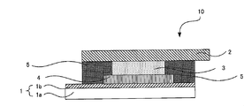
- FIG. 1 is a schematic cross-sectional view showing an example of the dye-sensitized solar cell of this embodiment.
- a dye-sensitized solar cell 10 according to this embodiment includes a base material 1 a and a base material for a dye-sensitized solar cell including the first electrode layer 1 b formed on the base material 1 a.
- a counter electrode base material 2 disposed so as to face the dye-sensitized solar cell base material 1 and having a function as an electrode, the dye-sensitized solar cell base material 1, and the counter electrode
- the electrolyte layer 3 formed between the base materials 2 and the first electrode layer 1b of the dye-sensitized solar cell base material 1 are formed so as to be in contact with the electrolyte layer 3, It has a porous layer 4 containing metal oxide semiconductor fine particles carrying a dye sensitizer on its surface, and a sealing material 5 formed so as to seal the electrolyte layer 3.
- the widths of the electrolyte layer 3 and the porous layer 4 are different, and the sealing material 5 is formed of the electrolyte layer 3 and the porous layer 4. An end portion is covered, and the electrolyte layer 3 is formed so as not to contact the first electrode layer 1b.
- the sealing material covers the end portions of the electrolyte layer and the porous layer, and is formed so that the electrolyte layer is not in contact with the first electrode layer.
- the location where the electrolyte layer directly contacts the first electrode layer (the interface indicated by B in FIG. 7A) can be eliminated.
- the interface distance between the porous layer and the sealing material can be increased by the difference in width between the electrolyte layer and the porous layer, the electrolyte layer has a gap between the porous layer and the sealing material. Even if it penetrates into the first electrode layer, it can be prevented from reaching the first electrode layer.
- One feature of the dye-sensitized solar cell of this embodiment is that the porous layer and the electrolyte layer have different widths.
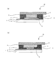
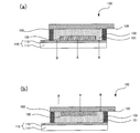
- FIG. 2 is a schematic cross-sectional view illustrating an embodiment in which the widths of the porous layer and the electrolyte layer are different in the dye-sensitized solar cell of this embodiment.
- the embodiment in which the width of the porous layer and the electrolyte layer is different is an embodiment in which the width of the porous layer 4 is wider than the width of the electrolyte layer 3.
- the width of the electrolyte layer 3 may be wider than the width of the porous layer 4 (FIG. 2B).
- the width of the porous layer and the electrolyte layer is different, any of the above embodiments can be suitably used.
- the width of the electrolyte layer is usually larger than the width of the porous layer.
- a narrow mode is preferred. This is because the dye-sensitized solar cell of this embodiment can be manufactured by a simple process.
- the difference in the width between the electrolyte layer and the porous layer in this aspect is that the interface distance between the porous layer and the sealing material is increased, and the electrolyte layer has penetrated into the gap between the porous layer and the sealing material. Also, there is no particular limitation as long as it can be prevented from reaching the first electrode layer.
- the specific difference in width is determined by the form and composition of the electrolyte layer and is not uniquely determined. In particular, in this embodiment, it is in the range of 0.5 mm to 5 mm. Is preferably in the range of 1 mm to 4 mm, more preferably in the range of 1 mm to 2 mm.
- the difference in width between the electrolyte layer and the porous layer is smaller than the above range, the interface distance between the porous layer and the sealing material is shortened, and the electrolyte layer penetrates into the gap between the porous layer and the sealing material, and the first This is because the electrolyte layer may reach the electrode layer and come into direct contact with the first electrode layer.
- the difference in width between the electrolyte layer and the porous layer is larger than the above range, the area of the porous layer that contributes to power generation decreases, and even if reverse electron transfer is prevented, a significant improvement in power generation efficiency may not be expected. Because there is sex.
- the difference in the width between the electrolyte layer and the porous layer means the distance from the end of the electrolyte layer to the end of the porous layer at an arbitrary end.
- FIG. 3 is a schematic diagram for explaining a difference in width between the electrolyte layer and the porous layer. As shown in FIGS. 3A and 3B, the difference in width between the electrolyte layer 3 and the porous layer 4 in this embodiment is the distance from the end of the electrolyte layer 3 to the end of the porous layer 4. X is meant.
- the electrolyte layer used in this embodiment is formed between the dye-sensitized solar cell substrate and the counter electrode substrate in the dye-sensitized solar cell of this embodiment. Further, the electrolyte layer used in this embodiment is characterized in that the width thereof is different from the width of the porous layer.
- the electrolyte layer used in this embodiment may be an electrolyte layer in any form of gel, solid or liquid. Further, the electrolyte layer used in this embodiment may contain a redox couple or may not contain it. When a redox couple is used, the redox couple used in this embodiment is not particularly limited as long as it is generally used in an electrolyte layer of a dye-sensitized solar cell. However, a combination of iodine and iodide and a combination of bromine and bromide are preferred.
- Examples of the combination of iodine and iodide used in this embodiment as the redox couple can be cited LiI, NaI, KI, and metal iodide such as CaI 2, a combination of I 2.
- examples of the combination of bromine and bromide include a combination of a metal bromide such as LiBr, NaBr, KBr, and CaBr 2 and Br 2 .
- the electrolyte layer when the electrolyte layer is in a liquid state, for example, acetonitrile, methoxyacetonitrile, propylene carbonate or the like is used as a solvent, and an oxidation-reduction pair is contained, or an ionic liquid having an imidazolium salt as a cation is used as the solvent. can do.
- the electrolyte layer when it is in a gel form, it may be either a physical gel or a chemical gel.
- the physical gel is gelled near room temperature due to physical interaction
- the chemical gel is a gel formed by chemical bonding by a crosslinking reaction or the like.
- a solid electrolyte layer what consists of CuI, a polypyrrole, polythiophene etc. can be mentioned, for example.
- the porous layer used in this embodiment contains metal oxide semiconductor fine particles having a dye sensitizer supported on the surface, and is formed on the first electrode layer of the dye-sensitized solar cell substrate described later. It is laminated and formed so as to be in contact with the electrolyte layer.
- the metal oxide semiconductor fine particles used in this embodiment are not particularly limited as long as they are made of a metal oxide having semiconductor characteristics.
- the metal oxide constituting the metal oxide semiconductor fine particles used in this embodiment include TiO 2 , ZnO, SnO 2 , ITO, ZrO 2 , MgO, Al 2 O 3 , CeO 2 , Bi 2 O 3 , and Mn. 3 O 4 , Y 2 O 3 , WO 3 , Ta 2 O 5 , Nb 2 O 5 , La 2 O 3 and the like can be mentioned.
- These metal oxide semiconductor fine particles are suitable for forming a porous porous layer, and can be suitably used in this embodiment because energy conversion efficiency can be improved and costs can be reduced.
- the metal oxide semiconductor fine particles used in this embodiment may be all made of the same metal oxide, or two or more kinds of different metal oxides may be used.
- the metal oxide semiconductor fine particles used in this embodiment may have a core-shell structure in which one type is a core fine particle and the other metal oxide semiconductor includes a core fine particle to form a shell.
- the average particle diameter of the metal oxide semiconductor fine particles used in this embodiment is not particularly limited as long as the specific surface area of the porous layer can be within a desired range, but is usually in the range of 1 nm to 10 ⁇ m.
- the inner diameter is preferably in the range of 10 nm to 1000 nm. If the average particle size is smaller than the above range, the respective metal oxide semiconductor fine particles may aggregate to form secondary particles. If the average particle size is larger than the above range, the porous layer becomes thicker. This is because the porosity of the porous layer, that is, the specific surface area may be reduced. Here, when the specific surface area of the porous layer becomes small, for example, it may be difficult to carry a dye sensitizer sufficient for photoelectric conversion on the porous layer.
- the average particle size of the metal oxide semiconductor fine particles means the primary particle size.
- all the metal oxide semiconductor fine particles having the same average particle diameter may be used, or two or more kinds of metal oxide semiconductor fine particles having different average particle diameters may be used.
- the metal oxide semiconductor fine particles having different average particle diameters By using together the metal oxide semiconductor fine particles having different average particle diameters, the light scattering effect in the porous layer can be enhanced, and the advantage that the dye-sensitized solar cell of this embodiment can be made more excellent in power generation efficiency. There is.
- examples of combinations of different average particle diameters include, for example, metal oxide semiconductor fine particles having an average particle diameter in the range of 10 nm to 50 nm.
- a combination with metal oxide semiconductor fine particles having an average particle diameter in the range of 50 nm to 800 nm can be exemplified.
- the dye sensitizer used in this embodiment is not particularly limited as long as it can absorb light and generate an electromotive force.
- a dye sensitizer include organic dyes and metal complex dyes.
- the organic dye include acridine, azo, indigo, quinone, coumarin, merocyanine, and phenylxanthene dyes. In this embodiment, among these organic dyes, a coumarin dye is preferably used.
- the metal complex dye it is preferable to use a ruthenium dye, and it is particularly preferable to use a ruthenium bipyridine dye and a ruthenium terpyridine dye which are ruthenium complexes. This is because such a ruthenium complex has a wide wavelength range of light to be absorbed, so that the wavelength range of light that can be photoelectrically converted can be greatly expanded.
- the porous layer used in this embodiment may contain an optional component in addition to the metal oxide semiconductor fine particles.
- binder resin can be mentioned, for example. This is because the porous layer used in this embodiment can be made less brittle by containing the binder resin in the porous layer.
- the binder resin that can be used for the porous layer in the present embodiment is not particularly limited as long as the brittleness of the porous layer can be set to a desired level. However, in this embodiment, since the porous layer is formed so as to be in contact with the electrolyte layer, it is necessary to use a binder resin having resistance to the electrolyte layer. Examples of such a binder resin include polyvinyl pyrrolidone, ethyl cellulose, caprolactan, and the like.
- binder resin used in this embodiment may be only one type, or two or more types.
- the thickness of the porous layer used in this embodiment can be appropriately determined according to the application of the dye-sensitized solar cell of this embodiment, and is not particularly limited.
- the thickness of the porous layer in this embodiment is usually preferably in the range of 1 ⁇ m to 100 ⁇ m, and particularly preferably in the range of 3 ⁇ m to 30 ⁇ m. This is because if the thickness of the porous layer is larger than the above range, the porous layer itself tends to cause cohesive failure, which tends to cause membrane resistance.
- the thickness of the porous layer is thinner than the above range, it becomes difficult to form a porous layer having a uniform thickness, or the amount of the dye sensitizer carried is reduced, so that the sunlight is sufficiently absorbed. This is because there is a possibility of poor performance because it is not possible.
- the porous layer in this embodiment may be composed of a single layer or may be composed of a plurality of layers.
- the porous layer having a configuration in which a plurality of layers are laminated any configuration can be appropriately selected and employed depending on the method for producing the dye-sensitized solar cell substrate used in this embodiment. .
- a configuration for example, an oxide semiconductor layer in contact with the first electrode layer and a porous layer formed on the oxide semiconductor layer and having a higher porosity than the oxide semiconductor layer.
- the aspect which is a 2 layer structure which consists of a layer can be mentioned.
- the porous layer used in this embodiment can be easily manufactured by a so-called transfer method. That is, the porous layer used in this embodiment is a method for forming a porous layer on a dye-sensitized solar cell substrate by firing on a heat-resistant substrate and then transferring these layers onto the substrate.
- the porous layer in this embodiment has a two-layer structure composed of the oxide semiconductor layer and the intervening layer, so that the performance of the porous layer can be reduced without reducing the performance of the porous layer. This is because the adhesion to the porous layer can be reduced, and as a result, the dye-sensitized solar cell substrate used in the present embodiment can be easily produced by the transfer method.
- the thickness ratio between the oxide semiconductor layer and the intervening layer is not particularly limited.
- the thickness of the intervening layer is preferably in the range of 10: 0.1 to 10: 5, and more preferably in the range of 10: 0.1 to 10: 3.
- the porosity of the oxide semiconductor layer is preferably in the range of 10% to 60%, and more preferably in the range of 20% to 50%. This is because if the porosity of the oxide semiconductor layer is smaller than the above range, for example, the porous layer may not be able to absorb sunlight effectively. Further, if it is larger than the above range, a desired amount of dye sensitizer may not be supported on the porous layer.
- the porosity of the intervening layer is not particularly limited as long as it is larger than the porosity of the oxide semiconductor layer. However, it is usually preferably in the range of 25% to 65%, and more preferably 30%. It is preferably in the range of ⁇ 60%.
- the porosity in this aspect shows the non-occupancy rate of the metal oxide semiconductor fine particles per unit volume.
- the porosity can be measured by a method in which the pore volume is measured with a gas adsorption amount measuring device (Autosorb-1MP; manufactured by Quantachrome) and calculated from the ratio to the volume per unit area.
- Autosorb-1MP gas adsorption amount measuring device
- the sealing material used in this embodiment covers the end portions of the electrolyte layer and the porous layer, and is formed so that the electrolyte layer does not contact the first electrode layer, so that the electrolyte layer and the first electrode It prevents the reverse electron transfer from being brought into direct contact with the layer and has a function of sealing the electrolyte layer.
- any material can be used without particular limitation as long as it is made of a material having durability with respect to the electrolyte layer.
- examples of such a sealing material include various heat-sealable thermoplastic resins or thermoplastic elastomers, low-density polyethylene, high-density polyethylene, polypropylene, poly-1-butene, poly-4-methyl-1-pentene, or ethylene.
- Polyolefin resins such as random or block copolymers of ⁇ -olefins such as propylene, 1-butene and 4-methyl-1-pentene; ethylene-vinyl acetate copolymer, ethylene-vinyl alcohol copolymer, ethylene -Ethylene-vinyl compound copolymer resin such as vinyl chloride copolymer; Styrenic resin such as polystyrene, acrylonitrile-styrene copolymer, ABS, ⁇ -methylstyrene-styrene copolymer; polyvinyl alcohol, polyvinylpyrrolidone, poly Vinyl chloride, polyvinylidene chloride , Vinyl chloride-vinylidene chloride copolymer, vinyl resins such as polyacrylic acid, polymethacrylic acid, polymethyl acrylate, polymethyl methacrylate; nylon 6, nylon 6-6, nylon 6-10, nylon 11, nylon Polyamide resins such as 12; Polyester resins such as poly
- the thickness of the sealing material used in this embodiment is usually preferably in the range of 1 ⁇ m to 100 ⁇ m, and more preferably in the range of 1 ⁇ m to 50 ⁇ m.
- the thickness of the sealing material in this embodiment corresponds to the distance between the dye-sensitized solar cell substrate and the counter electrode substrate.
- the base material for dye-sensitized solar cells used in this embodiment has a base material and a first electrode layer formed on the base material.
- each structure used for such a dye-sensitized solar cell substrate will be described in order.
- the base material used in this embodiment is not particularly limited as long as it has a self-supporting property that can support the first electrode layer and the porous layer used in this embodiment. Therefore, the base material used in this embodiment may be a flexible material having flexibility, or may be a rigid material having no flexibility, such as quartz glass, Pyrex (registered trademark), and synthetic quartz plate. May be.
- the base material used in this embodiment is preferably a flexible material, and among the flexible materials, a resin base material is preferable. This is because the resin base material is excellent in processability and can reduce the manufacturing cost.
- the resin base material examples include ethylene / tetrafluoroethylene copolymer film, biaxially stretched polyethylene terephthalate film, polyethersulfone (PES) film, polyetheretherketone (PEEK) film, and polyetherimide (PEI).
- PET polyimide
- PEN polyester naphthalate
- PC polycarbonate
- PET biaxially stretched polyethylene terephthalate film
- PEN polyester naphthalate film
- PC polycarbonate
- the thickness of the substrate used in this embodiment can be appropriately selected according to the use of the dye-sensitized solar cell of this embodiment, but is usually in the range of 50 ⁇ m to 2000 ⁇ m. In particular, it is preferably in the range of 75 ⁇ m to 1800 ⁇ m, and more preferably in the range of 100 ⁇ m to 1500 ⁇ m.
- the base material used for this aspect is excellent in heat resistance, a weather resistance, water vapor
- oxygen permeability is 1 cc / m 2 / day ⁇ atm or less under conditions of a temperature of 23 ° C. and a humidity of 90%, and a water vapor transmission rate of 1 g under conditions of a temperature of 37.8 ° C. and a humidity of 100%.
- a substrate provided with an arbitrary gas barrier layer may be used.
- the 1st electrode layer used for this mode is formed on the above-mentioned substrate.
- the material constituting the first electrode layer used in this embodiment is not particularly limited as long as it has a desired conductivity, and a conductive polymer material, a metal oxide, or the like can be used.
- the metal oxide is not particularly limited as long as it has desired conductivity.
- the metal oxide used in this embodiment has transparency to sunlight. Examples of such a metal oxide having transparency to sunlight include SnO 2 , ITO, IZO, and ZnO.
- any of these metal oxides can be suitably used, but among these, fluorine-doped SnO 2 (hereinafter referred to as FTO) and ITO are preferably used. This is because FTO and ITO are excellent in both conductivity and sunlight permeability.
- examples of the conductive polymer material include polythiophene, polyethylene sulfonic acid (PSS), polyaniline (PA), polypyrrole, and polyethylenedioxythiophene (PEDOT). Moreover, these can also be used in mixture of 2 or more types.
- the first electrode layer used in this embodiment may have a single layer structure or a structure in which a plurality of layers are stacked.
- Examples of the configuration in which a plurality of layers are stacked include a mode in which layers made of materials having different work functions are stacked, and a mode in which layers made of different metal oxides are stacked.
- the thickness of the 1st electrode layer used for this aspect will not be specifically limited if it exists in the range which can implement
- the thickness of the first electrode layer in this embodiment is usually preferably in the range of 5 nm to 2000 nm, and particularly preferably in the range of 10 nm to 1000 nm.
- the thickness is thicker than the above range, it may be difficult to form a uniform first electrode layer or the total light transmittance may be lowered, and it may be difficult to obtain good photoelectric conversion efficiency. This is because if the thickness is less than the above range, the conductivity of the first electrode layer may be insufficient.
- the said thickness shall point out the total thickness which totaled the thickness of all the layers, when a 1st electrode layer is comprised from a several layer.
- the substrate for a dye-sensitized solar cell used in this embodiment may be any substrate as long as it has at least the above-described substrate and the first electrode layer. It may have.
- an auxiliary electrode formed to be in contact with the first electrode layer and made of a conductive material can be given. By forming such an auxiliary electrode, if the conductivity of the first electrode layer is insufficient, it can be supplemented. Therefore, the dye-sensitized solar cell of this aspect can be made more efficient in power generation. There is an advantage that it can be made excellent.
- the counter electrode base material used in this embodiment has a function as an electrode.
- the counter electrode base material used in this embodiment is not particularly limited as long as it has a function as an electrode.
- Examples of such a counter electrode base material include those made of a metal foil and those having a configuration in which a second electrode layer is formed on a counter base material.
- the counter electrode substrate used in this embodiment When a substrate made of a metal foil is used as the counter electrode substrate used in this embodiment, it is not essential to have another configuration because the metal foil itself has a function as an electrode.
- the metal foil used as the counter electrode substrate include titanium, stainless steel, aluminum, copper, and the like.
- the thickness of the metal foil is not particularly limited as long as it is within a range in which desired self-supporting property can be imparted to the counter electrode substrate, Usually, it is preferably within the range of 5 ⁇ m to 1000 ⁇ m, more preferably within the range of 10 ⁇ m to 500 ⁇ m, and even more preferably within the range of 20 ⁇ m to 200 ⁇ m.
- the second electrode layer is made of a conductive material having a desired conductivity. If it is, it will not specifically limit, What consists of a conductive polymer material, a metal oxide, etc. can be used. Here, what was demonstrated as what is used for the said 1st electrode layer can be used about the said conductive polymer material and a metal oxide.
- the second electrode layer used in this embodiment may have a single layer configuration or a configuration in which a plurality of layers are stacked.
- Examples of the configuration in which a plurality of layers are laminated include an aspect in which layers made of materials having different work functions are laminated, and an aspect in which layers made of different metal oxides are laminated.
- the thickness of the second electrode layer used in this embodiment is usually preferably in the range of 5 nm to 2000 nm, and particularly preferably in the range of 10 nm to 1000 nm. Since the opposing base material used for this aspect can use the thing similar to the base material used for the said base material for dye-sensitized solar cells, description here is abbreviate
- omitted is abbreviate
- a catalyst layer may be formed on the counter electrode base material used in this embodiment as necessary.
- the dye-sensitized solar cell of this embodiment can be made more excellent in power generation efficiency.
- a catalyst layer include, for example, an embodiment in which Pt is vapor-deposited on the second electrode layer, polyethylene dioxythiophene (PEDOT), polystyrene sulfonic acid (PSS), polyaniline (PA), paratoluenesulfonic acid.
- PDOT polyethylene dioxythiophene
- PSS polystyrene sulfonic acid
- PA polyaniline
- paratoluenesulfonic acid paratoluenesulfonic acid.
- Embodiment of Dye-Sensitized Solar Cell includes a pair of base materials for a dye-sensitized solar cell and a substrate for the dye-sensitized solar cell that are patterned by the porous layer and the counter electrode substrate It may have a configuration in which a plurality of cells are connected between counter electrode substrates. This is because by having such a configuration, the dye-sensitized solar cell of this embodiment can have a high electromotive force.
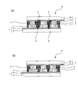
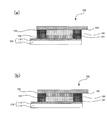
- FIG. 4 shows a case where a plurality of cells are connected to a pair of a dye-sensitized solar cell substrate and a counter electrode substrate when the counter electrode substrate having a counter substrate and a second electrode layer is used.
- FIG. 4 shows a configuration in which three cells are connected as an example.
- FIG. 4 (a) shows a mode of being connected in series
- FIG. 4 (b) shows a mode of being connected in parallel.
- 6 in Fig.4 (a) shows wiring.
- the patterning shape of the porous layer or the like can be arbitrarily determined depending on the electromotive force required for the dye-sensitized solar cell of this embodiment, but in this embodiment, the stripe shape is most preferable.
- the dye-sensitized solar cell of this aspect is produced, for example, by forming a porous layer on the dye-sensitized solar cell substrate and forming an electrolyte layer between the counter-electrode substrate. be able to.
- the method for forming the electrolyte layer between the dye-sensitized solar cell substrate and the counter electrode substrate is not particularly limited as long as the electrolyte layer can be formed with high thickness accuracy.
- a sealing material is formed so as to cover the periphery of the porous layer formed on the dye-sensitized solar cell substrate and the surface of the first electrode layer, and then the sealing material is used.
- An example is a method in which an electrolyte layer is formed on a porous layer on the inner side, and a counter electrode base material is disposed on the electrolyte layer.
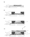
- FIG. 5 is a schematic view illustrating an example of the method for producing the dye-sensitized solar cell of this embodiment.
- the dye-sensitized solar cell 10 of the present embodiment prepares the dye-sensitized solar cell substrate 1 on which the porous layer 4 is laminated (FIG. 5A).
- a sealing material 5 is formed on the surface of one electrode layer 1b so as to surround the porous layer 4 (FIG. 5 (b)), and is an inner side surrounded by the sealing material 5 and on the porous layer 4
- An example is a method in which the electrolyte layer 3 is formed (FIG. 5C), and the counter electrode substrate 2 is further disposed on the electrolyte layer 3 (FIG. 5D).
- the dye-sensitized solar cell according to the second aspect of the present invention is a substrate, and a substrate for a dye-sensitized solar cell having a first electrode layer formed on the substrate, Formed between the counter electrode base material disposed as opposed to the dye-sensitized solar cell base material and having a function as an electrode, and the dye-sensitized solar cell base material and the counter electrode base material And a porous layer containing metal oxide semiconductor fine particles laminated on the counter electrode substrate and in contact with the electrolyte layer, and having a dye sensitizer supported on the surface.
- a sealing material formed so as to seal the electrolyte layer, wherein the electrolyte layer and the porous layer have different widths, and the sealing material includes the electrolyte layer and the porous material. Covering the edge of the layer, and further the electrolyte layer on the surface of the counter electrode substrate It is formed so as not to contact.
- FIG. 6 is a schematic cross-sectional view showing an example of the dye-sensitized solar cell of this embodiment.
- the dye-sensitized solar cell 10 of this embodiment includes a base material 1 a and a base material for a dye-sensitized solar cell including the first electrode layer 1 b formed on the base material 1 a.
- a counter electrode base material 2 disposed so as to face the dye-sensitized solar cell base material 1 and having a function as an electrode, the dye-sensitized solar cell base material 1, and the counter electrode
- An electrolyte layer 3 formed between the substrates 2 and a metal laminated on the counter electrode substrate 2 and in contact with the electrolyte layer 3 and having a dye sensitizer supported on the surface It has a porous layer 4 containing oxide semiconductor fine particles and a sealing material 5 formed so as to seal the electrolyte layer 3.
- the electrolyte layer 3 and the porous layer 4 have different widths
- the sealing material 5 is the electrolyte layer 3 and the porous layer 4.
- the electrolyte layer 3 is formed so as not to contact the surface of the counter electrode base material 2.
- the sealing material covers the ends of the electrolyte layer and the porous layer, and is formed so that the electrolyte layer is not in contact with the counter electrode base material.
- the location where the electrolyte layer directly contacts the counter electrode substrate (the interface indicated by B in FIG. 7B) can be eliminated.
- the interface distance between the porous layer and the sealing material can be increased, so that the electrolyte layer is placed in the gap between the sealing material and the porous layer. Even if it penetrates, it can prevent reaching the counter electrode substrate.
- the present invention it is possible to prevent reverse electron transfer due to direct contact between the electrolyte layer and the counter electrode substrate. For this reason, according to the present invention, it is possible to obtain a dye-sensitized solar cell in which reverse electron transfer is prevented by a simple method and the power generation efficiency is remarkably improved.
- Electrolyte Layer The electrolyte layer used in this embodiment is the same as that described in the section of “A. Dye-sensitized solar cell of the first embodiment”, and the description thereof is omitted here.
- the porous layer used in this embodiment contains metal oxide semiconductor fine particles having a dye sensitizer supported on the surface, and is laminated on the counter electrode substrate and formed so as to be in contact with the electrolyte layer. It is what is done.
- the porous layer used in this embodiment is not formed on the first electrode layer but on the counter electrode base material, except for the above-mentioned “A. Dye-sensitized solar cell of the first embodiment”. This is the same as described in the section.
- the sealing material used in this embodiment covers the end portions of the electrolyte layer and the porous layer, and is formed so that the electrolyte layer does not contact the counter electrode base material. This prevents the material from coming into direct contact and reverse electron transfer, and has a function of sealing the electrolyte layer.
- the sealing material used in this embodiment is not the first electrode layer but is formed so that the electrolyte layer is not in contact with the counter electrode base material. This is the same as that described in the section “Sensitive solar cell”.
- the dye-sensitized solar cell substrate used in this embodiment is the same as that described in the section “A. Dye-sensitized solar cell of the first embodiment” above. .
- the catalyst layer is formed on the said 1st electrode layer. By forming the catalyst layer on the first electrode layer, the dye-sensitized solar cell of this aspect can be made more excellent in power generation efficiency.
- Such a catalyst layer examples include, for example, an embodiment in which Pt is vapor-deposited on the first electrode layer, polyethylene dioxythiophene (PEDOT), polystyrene sulfonic acid (PSS), polyaniline (PA), paratoluenesulfonic acid.
- PDOT polyethylene dioxythiophene
- PSS polystyrene sulfonic acid
- PA polyaniline
- Pt polyethylene dioxythiophene
- PES polystyrene sulfonic acid
- PA polyaniline
- the thickness of Pt is 0.1 to 20 nm. preferable. If the thickness is less than 0.1 nm, the catalytic ability may be insufficient, and if it exceeds 20 nm, the amount of transmitted light may be insufficient.
- Counter Electrode Base Material The counter electrode base material used in this embodiment is the same as that described in the section “A. Dye-sensitized solar cell of the first embodiment” above.
- the dye-sensitized solar cell of this aspect is formed by patterning the porous layer and the first electrode layer of the dye-sensitized solar cell base material. It may have a configuration in which a plurality of cells are connected between a pair of dye-sensitized solar cell substrate and counter electrode substrate. This is because by having such a configuration, the dye-sensitized solar cell of this embodiment can have a high electromotive force.
- the manufacturing method of the dye-sensitized solar cell of this aspect is demonstrated.
- a porous layer is formed on the counter electrode substrate, and an electrolyte layer is formed between the dye-sensitized solar cell substrate and the counter electrode substrate.
- Such a method is the same as that described in the above section “A.
- Dye-sensitized solar cell of the first aspect” except that the porous layer is formed on the counter electrode substrate. The description in is omitted.
- the present invention is not limited to the above embodiment.
- the above-described embodiment is an exemplification, and the technical idea described in the claims of the present invention has substantially the same configuration and exhibits the same function and effect regardless of the case. It is included in the technical scope of the invention.
- Example 1 A glass substrate having a thickness of 1 mm is used as a base material.
- FTO is formed as a first electrode layer with a thickness of 400 nm by a sputtering method, and then cut into a 20 mm ⁇ 20 mm square, and a base material for a dye-sensitized solar cell Got.
- the surface resistivity of the first electrode layer was 10 ⁇ / ⁇ .
- an ink obtained by adding 4 wt% ethyl cellulose and ethanol to titanium oxide powder (Nippon Aerosil Co., Ltd .: P-25 (trade name)) is dried on the first electrode layer so that the thickness after drying is 8 ⁇ m.
- a porous layer was obtained by applying a film of 10 mm ⁇ 10 mm square and forming a film, followed by baking at 500 ° C. for 15 minutes.
- Ruthenium 535-bisTBA (trade name) manufactured by SOLARONIX as a dye sensitizer was dissolved in an ethanol solvent to prepare a dye solution having a concentration of 5 ⁇ 10 ⁇ 4 M.
- the porous layer was immersed in this dye solution for 12 hours to adsorb the dye to the porous layer, and then washed with ethanol and dried.
- a sealing material (Hi-Milan 25 ⁇ m manufactured by Mitsui-DuPont Polychemical Co., Ltd.) is disposed on the first electrode layer so as to cover the outer periphery of the porous layer by 2 mm, and the above-mentioned porous layer surrounded by the sealing material is placed on the porous layer.
- the electrolyte layer composition was laminated.
- a fluorine-doped tin oxide electrode in which platinum 15 nm is laminated by sputtering is used as the second electrode layer, and a counter electrode base material using a glass substrate as the counter base material is disposed so that the second electrode layer is in contact with the electrolyte layer. It was placed and heated at 170 ° C. for 1 minute to produce a dye-sensitized solar cell in the present invention.
- Example 2 A dye-sensitized solar cell was produced in the same manner as in Example 1 except that the electrolyte layer composition of Example 1 contained 5% by weight of ethyl cellulose.
- Example 3 A PEN substrate having a thickness of 100 ⁇ m was used as a base material, and ITO was formed on the base material as a first electrode layer with a thickness of 200 nm by an ion plating method. Subsequently, it cut out to 20 mm x 20 mm square. The surface resistivity of the first electrode layer was 15 ⁇ / ⁇ . Next, as a porous layer, a titanium oxide paste (manufactured by Solaronix: Ti-Nanoxide TL) is applied to the size of 10 mm ⁇ 10 mm square on the first electrode layer so that the thickness after drying becomes 8 ⁇ m. Then, a film was formed and dried at 150 ° C. for 1 hour to obtain a porous layer. Next, the dye was adsorbed on the porous layer in the same manner as in Example 1, and then washed with ethanol and dried.
- a titanium oxide paste manufactured by Solaronix: Ti-Nanoxide TL
- a sealing material (Mitsui / DuPont Polychemical Himiran 25 ⁇ m) is disposed on the first electrode layer so as to cover the outer peripheral portion of the porous layer by 2 mm, and Example 1 is formed on the porous layer surrounded by the sealing material.
- the electrolyte layer composition was laminated.
- a counter electrode base material using a fluorine-doped tin oxide electrode with platinum as a second electrode layer and a glass substrate as a counter base material is disposed so that the second electrode layer is in contact with the electrolyte layer.
- the dye-sensitized solar cell of the present invention was produced by heating at 3 ° C. for 3 minutes.
- Example 4 In Example 1, an 80 ⁇ m-thick titanium foil in which 15 nm of platinum was laminated by a sputtering method was used as a counter electrode base material, and platinum was placed in contact with the electrolyte layer. Moreover, it produced similarly to Example 1 except having arrange
- Example 5 Using a glass substrate having a thickness of 1 mm as a base material, ITO was formed as a first electrode layer with a thickness of 200 nm on the base material by sputtering, and then platinum was laminated on the first electrode layer with a thickness of 1 nm by sputtering. A 20 mm ⁇ 20 mm square was cut out to obtain a dye-sensitized solar cell substrate. The surface resistivity of the first electrode layer was 9 ⁇ / ⁇ .
- an ink obtained by adding 4 wt% ethyl cellulose and ethanol to titanium oxide powder is a counter electrode base material so that the thickness after drying becomes 7 ⁇ m.
- a porous layer was obtained by applying a film of 10 mm ⁇ 10 mm square onto a 80 ⁇ m thick titanium foil and baking at 500 ° C. for 15 minutes.
- the dye was adsorbed on the porous layer in the same manner as in Example 1, and then washed with ethanol and dried.
- 5 wt% ethyl cellulose was added to the electrolyte layer composition of Example 1 to obtain an electrolyte layer composition.
- a sealing material (Hi-Milan 25 ⁇ m manufactured by Mitsui-DuPont Polychemical Co., Ltd.) is arranged on the counter electrode base so as to cover the outer periphery of the porous layer by 1 mm, and the above-mentioned porous layer surrounded by the sealing material is placed on the porous layer.
- the electrolyte layer composition was laminated.
- the dye-sensitized solar cell substrate was placed so that platinum was in contact with the electrolyte layer, and heated at 170 ° C. for 1 minute to produce a dye-sensitized solar cell according to the present invention.
- Example 6 In Example 5, a PEN film having a thickness of 100 ⁇ m was used as a base material, ITO was formed as a first electrode layer with a thickness of 200 nm on the base material by an ion rating method, and then platinum was sputtered onto the first electrode layer. Then, the substrate was cut into a 20 mm ⁇ 20 mm square to obtain a dye-sensitized solar cell substrate. The surface resistivity of the first electrode layer was 15 ⁇ / ⁇ . Except that the dye-sensitized solar cell substrate was placed so that platinum was in contact with the electrolyte layer and heated at 140 ° C. for 3 minutes to produce the dye-sensitized solar cell in the present invention, as in Example 5. went.
- Example 7 In Example 5, it carried out like Example 5 except having laminated
- Example 8 In Example 5, it carried out like Example 5 except having laminated
- Example 1 In Example 1, it carried out like Example 1 except the magnitude
- Example 3 In Example 3, the same procedure as in Example 3 was performed, except that the size of the porous layer was 8 mm ⁇ 8 mm and the sealing material and the porous layer were spaced 1 mm apart.
- Example 8 it carried out similarly to Example 8 except having laminated
- Table 1 the evaluation result of the dye-sensitized solar cell produced by the Example and the comparative example is shown. Evaluation was performed immediately after producing the dye-sensitized solar cell and after storing it in an atmosphere at a temperature of 65 ° C. and a relative humidity of 60% for 168 hours. In the evaluation, when measuring the performance of the obtained dye-sensitized solar cell, the current-voltage characteristic when using artificial sunlight (AM1.5, irradiation intensity 100 mW / cm 2 ) as a light source is used as a source measure. It was determined by unit (Keutley Model 2400).
- SYMBOLS 1 Base material for dye-sensitized solar cells 1a ... Base material 1b ; 1st electrode layer 2 ... Counter electrode base material 2a ... Opposite base material 2b ... 2nd electrode layer 3 ... Electrolyte layer 4 ... Porous layer 5 ... Seal Material 6 ... Wiring 10 ... Dye-sensitized solar cell
Landscapes
- Engineering & Computer Science (AREA)
- Power Engineering (AREA)
- Chemical & Material Sciences (AREA)
- Chemical Kinetics & Catalysis (AREA)
- Electrochemistry (AREA)
- Microelectronics & Electronic Packaging (AREA)
- Photovoltaic Devices (AREA)
- Hybrid Cells (AREA)
Abstract
Description
このことは、図7(b)に例示した逆構造セル型の色素増感型太陽電池においても同様に当てはまり、電解質層と対電極基材とが接する界面における逆電子移動が発電効率を低下させる主たる要因であり、当該界面での逆電子移動を防止することにより著しく発電効率を改善することができることを見出した。
また、上記電解質層と上記多孔質層との幅が異なっていることにより、多孔質層とシール材との界面距離を長くすることができるため、電解質層がシール材と多孔質層の隙間に染み込んだとしても第1電極層に到達することを防止することができる。このため、本発明によれば電解質層と第1電極層とが直接的に接することによる逆電子移動を防止できる。
このようなことから本発明によれば、簡易な方法で逆電子移動を防止し、発電効率が著しく改善された色素増感型太陽電池を得ることができる。
また、上記電解質層と上記多孔質層との幅が異なっていることにより、多孔質層とシール材との界面距離を長くすることができるため、電解質層がシール材と多孔質層の隙間に染み込んだとしても対電極基材に到達することを防止することができる。このため、本発明によれば電解質層と対電極基材とが直接的に接することによる逆電子移動を防止できる。
このようなことから本発明によれば、簡易な方法で逆電子移動を防止し、発電効率が著しく改善された色素増感型太陽電池を得ることができる。
したがって、以下、各態様に分けて本発明の色素増感型太陽電池について説明する。
1.色素増感型太陽電池
本発明の第1態様の色素増感型太陽電池は、基材、および上記基材上に形成された第1電極層を有する色素増感型太陽電池用基材と、上記色素増感型太陽電池用基材に対向するように配置され、電極としての機能を備える対電極基材と、上記色素増感型太陽電池用基材および上記対電極基材の間に形成された電解質層と、上記色素増感型太陽電池用基材の第1電極層上に積層され、かつ上記電解質層と接するように形成されており、表面に色素増感剤が担持された金属酸化物半導体微粒子を含む多孔質層と、上記電解質層を封止するように形成されたシール材とを有するものであって、上記電解質層と上記多孔質層の幅が異なっており、かつ上記シール材が上記電解質層および多孔質層の端部を覆い、さらに上記第1電極層に上記電解質層が接しないように形成されていることを特徴とするものである。
このような例において、本態様の色素増感型太陽電池10は、上記電解質層3と上記多孔質層4の幅が異なっており、かつシール材5が上記電解質層3および多孔質層4の端部を覆い、さらに上記第1電極層1bに上記電解質層3が接しないように形成されていることを特徴とするものである。
また、上記電解質層と上記多孔質層との幅が異なっていることにより、多孔質層とシール材との界面距離を長くすることができるため、電解質層が多孔質層とシール材との隙間に染み込んだとしても第1電極層に到達することを防止することができる。このため、本態様によれば電解質層と第1電極層とが直接的に接することによる逆電子移動を防止できる。
このようなことから本態様によれば、簡易な方法で逆電子移動を防止し、発電効率が著しく改善された色素増感型太陽電池を得ることができる。
次に、本態様に用いられる電解質層について説明する。本態様に用いられる電解質層は、本態様の色素増感型太陽電池において色素増感型太陽電池用基材と対電極基材との間に形成されるものである。また、本態様に用いられる電解質層は、その幅が多孔質層の幅と異なるように形成されていることを特徴とするものである。
さらに、上記臭素および臭化物の組合せとしては、例えば、LiBr、NaBr、KBr、CaBr2等の金属臭化物と、Br2との組合せを挙げることができる。
また、固体状の電解質層としては、例えば、CuI、ポリピロール、ポリチオフェン等からなるものを挙げることができる。
次に、本態様に用いられる多孔質層について説明する。本態様に用いられる多孔質層は、表面に色素増感剤が担持された金属酸化物半導体微粒子を含有するものであり、後述する色素増感型太陽電池用基材の第1電極層上に積層され、かつ上記電解質層に接するように形成されるものである。
本態様に用いられる金属酸化物半導体微粒子としては、半導体特性を備える金属酸化物からなるものであれば特に限定されるものではない。本態様に用いられる金属酸化物半導体微粒子を構成する金属酸化物としては、例えば、TiO2、ZnO、SnO2、ITO、ZrO2、MgO、Al2O3、CeO2、Bi2O3、Mn3O4、Y2O3、WO3、Ta2O5、Nb2O5、La2O3等を挙げることができる。これらの金属酸化物半導体微粒子は、多孔性の多孔質層を形成するのに適しており、エネルギー変換効率の向上、コストの削減を図ることができるため本態様に好適に用いられる。
なかでも本態様においてはTiO2からなる金属酸化物半導体微粒子を用いることが最も好ましい。TiO2は特に半導体特性に優れるからである。
なお、上記金属酸化物半導体微粒子の平均粒径は一次粒径を意味するものとする。
本態様に用いられる色素増感剤としては、光を吸収して起電力を生じさせることが可能なものであれば特に限定はされない。このような色素増感剤としては、有機色素または金属錯体色素を挙げることができる。上記有機色素としては、アクリジン系、アゾ系、インジゴ系、キノン系、クマリン系、メロシアニン系、フェニルキサンテン系の色素が挙げられる。本態様においてはこれらの有機色素の中でも、クマリン系色素を用いることが好ましい。また、上記金属錯体色素としてはルテニウム系色素を用いることが好ましく、特にルテニウム錯体であるルテニウムビピリジン色素およびルテニウムターピリジン色素を用いることが好ましい。このようなルテニウム錯体は吸収する光の波長範囲が広いため、光電変換できる光の波長領域を大幅に広げることができるからである。
本態様に用いられる多孔質層には、上記金属酸化物半導体微粒子の他に任意の成分が含まれていてもよい。本態様に用いられる任意の成分としては、例えば、バインダー樹脂を挙げることができる。上記多孔質層にバインダー樹脂が含有されることにより、本態様に用いられる多孔質層を脆性の低いものにできるからである。
本態様に用いられる多孔質層の厚みは、本態様の色素増感型太陽電池の用途に応じて、適宜決定できるものであり特に限定されるものではい。なかでも本態様における多孔質層の厚みは、通常、1μm~100μmの範囲内であることが好ましく、特に3μm~30μmの範囲内であることが好ましい。多孔質層の厚みが上記範囲よりも厚いと、多孔質層自体の凝集破壊が起りやすく、膜抵抗となりやすくなってしまう場合があるからである。また、多孔質層の厚みが上記範囲よりも薄いと厚みが均一な多孔質層を形成するのが困難となったり、色素増感剤が担持される量が少なくなり、太陽光を十分に吸収できないために性能不良になる可能性があるからである。
次に、本態様に用いられるシール材について説明する。本態様に用いられるシール材は、上記電解質層および多孔質層の端部を覆い、さらに上記第1電極層に上記電解質層が接しないように形成されていることにより、電解質層と第1電極層とが直接的に接触して逆電子移動が生じることを防止するとともに、電解質層を封止する機能を有するものである。
次に、本態様に用いられる色素増感型太陽電池用基材について説明する。本態様に用いられる色素増感型太陽電池用基材は、基材と、上記基材上に形成された第1電極層とを有するものである。
以下、このような色素増感型太陽電池用基材に用いられる各構成について順に説明する。
まず、本態様に用いられる基材について説明する。本態様に用いられる基材としては、本態様に用いられる第1電極層、および多孔質層を支持することが可能な程度の自己支持性を有するものであれば特に限定されるものではない。したがって、本態様に用いられる基材は可撓性を有するフレキシブル材であってもよく、または、石英ガラス、パイレックス(登録商標)、合成石英板等の可撓性を有さないリジッド材であってもよい。なかでも本態様に用いられる基材はフレキシブル材であることが好ましく、上記フレキシブル材のなかでも樹脂製基材であることが好ましい。樹脂製基材は加工性に優れ、製造コストの低減ができるからである。
次に、本態様に用いられる第1電極層について説明する。本態様に用いられる第1電極層は、上記基材上に形成されたものである。
上記金属酸化物としては、所望の導電性を有するものであれば特に限定されるものではない。なかでも本態様に用いられる金属酸化物は太陽光に対して透過性を有するものであることが好ましい。このような太陽光に対する透過性を有する金属酸化物としては、例えば、SnO2、ITO、IZO、ZnOを挙げることができる。本態様においては、これらのいずれの金属酸化物であっても好適に用いることができるが、なかでもフッ素ドープしたSnO2(以下、FTOと称する。)、ITOを用いることが好ましい。FTOおよびITOは、導電性および太陽光の透過性の両方に優れているからである。
一方、上記導電性高分子材料としては、例えば、ポリチオフェン、ポリエチレンスルフォン酸(PSS)、ポリアニリン(PA)、ポリピロール、ポリエチレンジオキシチオフェン(PEDOT)等を挙げることができる。また、これらを2種以上混合して用いることもできる。
なお、上記厚みは、第1電極層が複数の層から構成される場合には、すべての層の厚みを合計した総厚みを指すものとする。
本態様に用いられる色素増感型太陽電池用基材は、少なくとも上記基材、および第1電極層を有するものであればよいが、必要に応じて他の任意の構成を有してもよいものである。本態様に用いられる任意の構成としては、例えば、上記第1電極層に接するように形成され、導電性材料からなる補助電極を挙げることができる。このような補助電極が形成されていることにより、上記第1電極層の導電性が不足する場合に、それを補充することができるため、本態様の色素増感型太陽電池をより発電効率に優れたものにできるという利点がある。
上記色素増感型太陽電池用基材の製造方法としては、上述した構成を有する色素増感型太陽電池用基材を製造できる方法であれば特に限定されるものではなく、一般的に公知の方法を適宜参考にして用いることができる。
次に、本態様に用いられる対電極基材について説明する。本態様における対電極基材は、電極としての機能を有するものである。
本態様に用いられる対向基材は、上記色素増感型太陽電池用基材に用いられる基材と同様のものを用いることができるため、ここでの説明は省略する。
本態様の色素増感型太陽電池は、上記多孔質層、および上記対電極基材がパターニングされていることにより、一対の色素増感型太陽電池用基材および対電極基材の間に複数のセルが連結された構成を有するものであってもよい。このような構成を有することにより、本態様の色素増感型太陽電池を起電力の高いものにできるからである。
図4は、上記対電極基材として対向基材と第2電極層とを有するものが用いられる場合において、一対の色素増感型太陽電池用基材および対電極基材に複数のセルが連結された構成を有する場合の一例を示す概略断面図である。図4は、一例として3つのセルが連結した構成を有するものであり、図4(a)は、直列に連結された態様、図4(b)は並列に連結された態様を示すものである。なお、図4(a)における6は配線を示す。
次に、本態様の色素増感型太陽電池の製造方法について説明する。本態様の色素増感型太陽電池は、例えば、上記色素増感型太陽電池用基材上に多孔質層を形成し、上記対電極基材との間に電解質層を形成することにより製造することができる。
1.色素増感型太陽電池
本発明の第2態様の色素増感型太陽電池は、基材、および上記基材上に形成された第1電極層を有する色素増感型太陽電池用基材と、上記色素増感型太陽電池用基材に対向するように配置され、電極としての機能を備える対電極基材と、上記色素増感型太陽電池用基材および上記対電極基材の間に形成された電解質層と、上記対電極基材上に積層され、かつ上記電解質層と接するように形成されており、表面に色素増感剤が担持された金属酸化物半導体微粒子を含む多孔質層と、上記電解質層を封止するように形成されたシール材と、を有するものであって、上記電解質層と上記多孔質層の幅が異なっており、かつ上記シール材が上記電解質層および多孔質層の端部を覆い、さらに上記対電極基材の表面に上記電解質層が接しないように形成されていることを特徴とするものである。
このような例において、本態様の色素増感型太陽電池10は、上記電解質層3と上記多孔質層4の幅が異なっており、かつ上記シール材5が上記電解質層3および多孔質層4の端部を覆い、さらに上記対電極基材2の表面に上記電解質層3が接しないように形成されていることを特徴とするものである。
また、上記電解質層と上記多孔質層との幅が異なっていることにより、多孔質層とシール材との界面距離を長くすることができるため、電解質層がシール材と多孔質層の隙間に染み込んだとしても対電極基材に到達することを防止することができる。このため、本発明によれば電解質層と対電極基材とが直接的に接することによる逆電子移動を防止できる。
このようなことから本発明によれば、簡易な方法で逆電子移動を防止し、発電効率が著しく改善された色素増感型太陽電池を得ることができる。
本態様に用いられる電解質層は、上記「A.第1態様の色素増感型太陽電池」の項において説明したものと同様であるため、ここでの説明は省略する。
次に、本態様に用いられる多孔質層について説明する。本態様に用いられる多孔質層は、表面に色素増感剤が担持された金属酸化物半導体微粒子を含有するものであり、対電極基材上に積層され、かつ上記電解質層に接するように形成されるものである。なお、本態様に用いられる多孔質層は、第1電極層上ではなく、対電極基材上に積層されていること以外は、上記「A.第1態様の色素増感型太陽電池」の項において説明したものと同様である。
次に、本態様に用いられるシール材について説明する。本態様に用いられるシール材は、上記電解質層および多孔質層の端部を覆い、さらに上記対電極基材に上記電解質層が接しないように形成されていることにより、電解質層と対電極基材とが直接的に接触して逆電子移動が生じることを防止するとともに、電解質層を封止する機能を有するものである。
ここで、本態様に用いられるシール材は、第1電極層ではなく上記対電極基材に上記電解質層が接しないように形成されていること以外は、上記「A.第1態様の色素増感型太陽電池」の項において説明したものと同様である。
本態様に用いられる色素増感型太陽電池用基材は、上記「A.第1態様の色素増感型太陽電池」の項において説明したものと同様である。
なお、本態様に用いられる色素増感型太陽電池用基材は、上記第1電極層上に触媒層が形成されていることが好ましい。上記第1電極層上に触媒層が形成されていることにより、本態様の色素増感型太陽電池をより発電効率に優れたものにできる。このような触媒層の例としては、例えば、上記第1電極層上にPtを蒸着した態様や、ポリエチレンジオキシチオフェン(PEDOT)、ポリスチレンスルフォン酸(PSS)、ポリアニリン(PA)、パラトルエンスルホン酸(PTS)およびこれらの混合物から触媒層を形成する態様を挙げることができるがこの限りではない。上記第1電極層上に触媒層を形成する場合、光透過性を損なわない範囲で触媒能を発揮させる必要があり、例えば、Ptを蒸着した態様では、Ptの厚みは0.1~20nmが好ましい。0.1nmを下回る場合、触媒能が不足する可能性があり、20nmを上回る場合は透過する光の量が不足する可能性がある。
本態様に用いられる対電極基材は、上記「A.第1態様の色素増感型太陽電池」の項において説明したものと同様である。
本態様の色素増感型太陽電池は、多孔質層等、および、上記色素増感型太陽電池用基材の第1電極層等がパターニングされていることにより、一対の色素増感型太陽電池用基材および対電極基材の間に複数のセルが連結された構成を有するものであってもよい。このような構成を有することにより、本態様の色素増感型太陽電池を起電力の高いものにできるからである。
次に、本態様の色素増感型太陽電池の製造方法について説明する。本態様の色素増感型太陽電池は、例えば、上記対電極基材上に多孔質層形成し、色素増感型太陽電池用基材と、対電極基材との間に電解質層を形成することにより製造することができる。このような方法は、多孔質層を対電極基材上に形成すること以外は、上記「A.第1態様の色素増感型太陽電池」の項において説明したものと同様であるため、ここでの説明は省略する。
1mm厚のガラス基板を基材として用い、当該基材上に、第1電極層としてFTOをスパッタ法で厚み400nmで形成し、次いで20mm×20mm角に切り出し、色素増感型太陽電池用基材を得た。第1電極層の表面抵抗率は10Ω/□であった。
次に、酸化チタン粉末(日本アエロジル社製:P-25(商品名))に4wt%のエチルセルロースとエタノールとを添加したインキを、乾燥後の厚みが8μmとなるよう、第1電極層上に10mm×10mm角の大きさに塗布して成膜し、500℃で15分焼成することにより多孔質層を得た。
次に、色素増感剤として、SOLARONIX社製のRuthenium535-bisTBA(商品名)を、エタノール溶剤に溶解し、濃度5×10⁻⁴Mに調製して色素溶液とした。この色素溶液に上記多孔質層を12時間浸漬して多孔質層に色素を吸着させ、その後エタノールで洗浄して乾燥させた。
次に、1-メチル-3-プロピルイミダゾリウムアイオダイド(8g)と、プロピオニトリル(2g)の混合溶液に脂環式エポキシ樹脂(0.5g、ダイセル化学社製の商品名;2021)とシリコーン樹脂(0.5g、東レシリコーン社製のSH6018)を加えて溶解し、また、ヨウ素をヨウ素濃度が0.03Mになるように溶解させ、電解質層組成物とした。
次に、上記多孔質層の外周部を2mm覆うように第1電極層上にシール材(三井・デュポンポリケミカル社製ハイミラン25μm)を配し、シール材に囲まれた多孔質層上に上記電解質層組成物を積層した。
次に、白金15nmをスパッタ法で積層したフッ素ドープ酸化錫電極を第2電極層とし、ガラス基板を対向基材として用いた対電極基材を、上記第2電極層が電解質層と接するように配置し、170℃、1分加熱して本発明における色素増感型太陽電池を作製した。
実施例1の電解質層組成物に、エチルセルロース5wt%を含有させたこと以外は、実施例1と同様の方法により色素増感型太陽電池を作製した。
100μ厚のPEN基板を基材として用い、当該基材上に第1電極層としてITOをイオンプレーティング法で厚み200nm形成した。次いで、20mm×20mm角に切り出した。第1電極層の表面抵抗率は15Ω/□であった。
次に、多孔質層として、酸化チタンペースト(Solaronix社製:Ti-Nanoxide T-L)を、乾燥後の厚みが8μmとなるよう、第1電極層上に10mm×10mm角の大きさに塗布して成膜し、150℃で1時間乾燥させて多孔質層とした。
次に、実施例1と同様にして多孔質層に色素を吸着させ、その後エタノールで洗浄して乾燥させた。
次に、白金をつけたフッ素ドープ酸化錫電極を第2電極層とし、ガラス基板を対向基材として用いた対電極基材を、上記第2電極層が電解質層と接するように配置し、140℃、3分加熱して本発明における色素増感型太陽電池を作製した。
実施例1において、白金15nmをスパッタ法で積層した80μm厚のチタン箔を対電極基材とし、白金を電解質層と接するように配置した。また、多孔質層の外周部を1mm覆うように第1電極層上にシール材(三井・デュポンポリケミカル社製ハイミラン25μm)を配した他は、実施例1と同様に作製した。
1mm厚のガラス基板を基材として用い、当該基材上に第1電極層としてITOをスパッタ法で厚み200nmで形成し、次いで上記第1電極層上に白金をスパッタ法で1nm積層した後、20mm×20mm角に切り出し、色素増感型太陽電池用基材を得た。第1電極層の表面抵抗率は9Ω/□であった。
次に、酸化チタン粉末(日本アエロジル社製:P-25(商品名))に4wt%のエチルセルロースとエタノールとを添加したインキを、乾燥後の厚みが7μmとなるよう、対電極基材である80μm厚のチタン箔上に10mm×10mm角の大きさに塗布して成膜し、500℃で15分焼成することにより多孔質層を得た。
次に、実施例1と同様にして多孔質層に色素を吸着させ、その後エタノールで洗浄して乾燥させた。
次に、実施例1の電解質層組成物にエチルセルロース5wt%を含有させ、電解質層組成物とした。
次に、上記多孔質層の外周部を1mm覆うように対電極基材上にシール材(三井・デュポンポリケミカル社製ハイミラン25μm)を配し、シール材に囲まれた多孔質層上に上記電解質層組成物を積層した。
次に、色素増感型太陽電池用基材を、白金が電解質層と接するよう配置し、170℃、1分加熱して本発明における色素増感型太陽電池を作製した。
実施例5において、100μm厚のPENフィルムを基材として用い、当該基材上に、第1電極層としてITOをイオンレーティング法で厚み200nm形成し、次いで上記第1電極層上に白金をスパッタ法で1nm積層した後、20mm×20mm角に切り出し、色素増感型太陽電池用基材を得た。第1電極層の表面抵抗率は15Ω/□であった。色素増感型太陽電池用基材を、白金が電解質層と接するよう配置し、140℃、3分加熱して本発明における色素増感型太陽電池を作製した他は、実施例5と同様に行った。
実施例5において、白金をスパッタ法で5nm積層した他は、実施例5と同様に行った。
実施例5において、白金をスパッタ法で10nm積層した他は、実施例5と同様に行った。
実施例1において、多孔質層の大きさを8mm×8mmとし、シール材と多孔質層の間を1mm空けた他は実施例1と同様に行った。
実施例3において、多孔質層の大きさを8mm×8mmとし、シール材と多孔質層の間を1mm空けた他は実施例3と同様に行った。
実施例8において、白金をスパッタ法で10nm積層し、多孔質層の大きさを8mm×8mmとし、シール材と多孔質層の間を1mm空けた他は、実施例8と同様に行った。

1a … 基材
1b … 第1電極層
2 … 対電極基材
2a … 対向基材
2b … 第2電極層
3 … 電解質層
4 … 多孔質層
5 … シール材
6 … 配線
10 … 色素増感型太陽電池
Claims (4)
- 基材、および前記基材上に形成された第1電極層を有する色素増感型太陽電池用基材と、
前記色素増感型太陽電池用基材に対向するように配置され、電極としての機能を備える対電極基材と、
前記色素増感型太陽電池用基材および前記対電極基材の間に形成された電解質層と、
前記色素増感型太陽電池用基材の第1電極層上に積層され、かつ前記電解質層と接するように形成されており、表面に色素増感剤が担持された金属酸化物半導体微粒子を含む多孔質層と、
前記電解質層を封止するように形成されたシール材と、
を有する色素増感型太陽電池であって、
前記電解質層と前記多孔質層の幅が異なっており、かつ前記シール材が前記電解質層および前記多孔質層の端部を覆い、さらに前記第1電極層に前記電解質層が接しないように形成されていることを特徴とする色素増感型太陽電池。 - 基材、および前記基材上に形成された第1電極層を有する色素増感型太陽電池用基材と、
前記色素増感型太陽電池用基材に対向するように配置され、電極としての機能を備える対電極基材と、
前記色素増感型太陽電池用基材および前記対電極基材の間に形成された電解質層と、
前記対電極基材上に積層され、かつ前記電解質層と接するように形成されており、表面に色素増感剤が担持された金属酸化物半導体微粒子を含む多孔質層と、
前記電解質層を封止するように形成されたシール材と、
を有する色素増感型太陽電池であって、
前記電解質層と前記多孔質層の幅が異なっており、かつ前記シール材が前記電解質層および前記多孔質層の端部を覆い、さらに前記対電極基材の表面に前記電解質層が接しないように形成されていることを特徴とする色素増感型太陽電池。 - 前記電解質層の幅が前記多孔質層の幅よりも狭いことを特徴とする、請求の範囲第1項または第2項に記載の色素増感型太陽電池。
- 前記電解質層と前記多孔質層との幅の差が0.5mm~5mmの範囲内であることを特徴とする、請求の範囲第1項から第3項までのいずれかに記載の色素増感型太陽電池。
Priority Applications (2)
| Application Number | Priority Date | Filing Date | Title |
|---|---|---|---|
| CN201080037153.3A CN102549835B (zh) | 2009-09-30 | 2010-07-06 | 色素敏化型太阳能电池 |
| US13/386,999 US20120118379A1 (en) | 2009-09-30 | 2010-07-06 | Dye-sensitized solar cell |
Applications Claiming Priority (2)
| Application Number | Priority Date | Filing Date | Title |
|---|---|---|---|
| JP2009227758A JP4900443B2 (ja) | 2009-09-30 | 2009-09-30 | 色素増感型太陽電池 |
| JP2009-227758 | 2009-09-30 |
Publications (1)
| Publication Number | Publication Date |
|---|---|
| WO2011040102A1 true WO2011040102A1 (ja) | 2011-04-07 |
Family
ID=43825937
Family Applications (1)
| Application Number | Title | Priority Date | Filing Date |
|---|---|---|---|
| PCT/JP2010/061487 Ceased WO2011040102A1 (ja) | 2009-09-30 | 2010-07-06 | 色素増感型太陽電池 |
Country Status (4)
| Country | Link |
|---|---|
| US (1) | US20120118379A1 (ja) |
| JP (1) | JP4900443B2 (ja) |
| CN (1) | CN102549835B (ja) |
| WO (1) | WO2011040102A1 (ja) |
Cited By (5)
| Publication number | Priority date | Publication date | Assignee | Title |
|---|---|---|---|---|
| JP2013201078A (ja) * | 2012-03-26 | 2013-10-03 | Sekisui Chem Co Ltd | 電気モジュール及び電気モジュールの製造方法 |
| JP2013201079A (ja) * | 2012-03-26 | 2013-10-03 | Sekisui Chem Co Ltd | 電気モジュール及び電気モジュールの製造方法 |
| JP2016143822A (ja) * | 2015-02-04 | 2016-08-08 | 株式会社フジクラ | 光電変換素子 |
| JP2016143823A (ja) * | 2015-02-04 | 2016-08-08 | 株式会社フジクラ | 光電変換素子 |
| WO2016125846A1 (ja) * | 2015-02-04 | 2016-08-11 | 株式会社フジクラ | 光電変換素子 |
Families Citing this family (5)
| Publication number | Priority date | Publication date | Assignee | Title |
|---|---|---|---|---|
| JP5536015B2 (ja) * | 2011-11-21 | 2014-07-02 | シャープ株式会社 | 光電変換素子および光電変換素子モジュール |
| JP2013235787A (ja) * | 2012-05-11 | 2013-11-21 | Hitachi Zosen Corp | 色素増感太陽電池およびその製造方法 |
| GB201312317D0 (en) | 2013-07-09 | 2013-08-21 | Syntaxin Ltd | Cationic neurotoxins |
| EP3067906A4 (en) * | 2013-11-08 | 2016-10-12 | Panasonic Corp | ELECTROCHEMICAL DEVICE |
| JP7164362B2 (ja) * | 2018-09-03 | 2022-11-01 | 積水化学工業株式会社 | 電気モジュール |
Citations (4)
| Publication number | Priority date | Publication date | Assignee | Title |
|---|---|---|---|---|
| JP2002151168A (ja) * | 2000-11-13 | 2002-05-24 | Sharp Corp | 色素増感型太陽電池 |
| JP2006236788A (ja) * | 2005-02-25 | 2006-09-07 | Sony Corp | 光電変換装置 |
| JP2009032608A (ja) * | 2007-07-30 | 2009-02-12 | Kyocera Corp | 光電変換装置及び光発電装置 |
| JP2009059782A (ja) * | 2007-08-30 | 2009-03-19 | Kyocera Corp | 光電変換装置 |
Family Cites Families (5)
| Publication number | Priority date | Publication date | Assignee | Title |
|---|---|---|---|---|
| WO2001048833A1 (en) * | 1999-12-27 | 2001-07-05 | Seiko Epson Corporation | Solar cell and solar cell unit |
| JP4638973B2 (ja) * | 2000-03-27 | 2011-02-23 | 富士フイルム株式会社 | 光電変換素子および光電池 |
| US7202412B2 (en) * | 2002-01-18 | 2007-04-10 | Sharp Kabushiki Kaisha | Photovoltaic cell including porous semiconductor layer, method of manufacturing the same and solar cell |
| JP5266524B2 (ja) * | 2007-08-06 | 2013-08-21 | 東洋製罐グループホールディングス株式会社 | 色素増感型太陽電池用電極基板及び色素増感型太陽電池 |
| JP2009129574A (ja) * | 2007-11-20 | 2009-06-11 | Toyo Seikan Kaisha Ltd | 色素増感型太陽電池 |
-
2009
- 2009-09-30 JP JP2009227758A patent/JP4900443B2/ja not_active Expired - Fee Related
-
2010
- 2010-07-06 CN CN201080037153.3A patent/CN102549835B/zh not_active Expired - Fee Related
- 2010-07-06 WO PCT/JP2010/061487 patent/WO2011040102A1/ja not_active Ceased
- 2010-07-06 US US13/386,999 patent/US20120118379A1/en not_active Abandoned
Patent Citations (4)
| Publication number | Priority date | Publication date | Assignee | Title |
|---|---|---|---|---|
| JP2002151168A (ja) * | 2000-11-13 | 2002-05-24 | Sharp Corp | 色素増感型太陽電池 |
| JP2006236788A (ja) * | 2005-02-25 | 2006-09-07 | Sony Corp | 光電変換装置 |
| JP2009032608A (ja) * | 2007-07-30 | 2009-02-12 | Kyocera Corp | 光電変換装置及び光発電装置 |
| JP2009059782A (ja) * | 2007-08-30 | 2009-03-19 | Kyocera Corp | 光電変換装置 |
Cited By (6)
| Publication number | Priority date | Publication date | Assignee | Title |
|---|---|---|---|---|
| JP2013201078A (ja) * | 2012-03-26 | 2013-10-03 | Sekisui Chem Co Ltd | 電気モジュール及び電気モジュールの製造方法 |
| JP2013201079A (ja) * | 2012-03-26 | 2013-10-03 | Sekisui Chem Co Ltd | 電気モジュール及び電気モジュールの製造方法 |
| JP2016143822A (ja) * | 2015-02-04 | 2016-08-08 | 株式会社フジクラ | 光電変換素子 |
| JP2016143823A (ja) * | 2015-02-04 | 2016-08-08 | 株式会社フジクラ | 光電変換素子 |
| WO2016125846A1 (ja) * | 2015-02-04 | 2016-08-11 | 株式会社フジクラ | 光電変換素子 |
| US10692658B2 (en) | 2015-02-04 | 2020-06-23 | Fujikura Ltd. | Photoelectric conversion element |
Also Published As
| Publication number | Publication date |
|---|---|
| JP4900443B2 (ja) | 2012-03-21 |
| CN102549835B (zh) | 2015-04-01 |
| JP2011076893A (ja) | 2011-04-14 |
| CN102549835A (zh) | 2012-07-04 |
| US20120118379A1 (en) | 2012-05-17 |
Similar Documents
| Publication | Publication Date | Title |
|---|---|---|
| JP4900443B2 (ja) | 色素増感型太陽電池 | |
| JP5678345B2 (ja) | 色素増感太陽電池およびその製造方法 | |
| JP5531300B2 (ja) | 色素増感太陽電池 | |
| TW201117455A (en) | Dye-sensitized photoelectric conversion element, method of manufacturing the same and electronic equipment | |
| JP2007073505A (ja) | 光電変換素子 | |
| JP2004363069A (ja) | 半導体電極およびその製造方法、ならびにそれを用いた色素増感型太陽電池 | |
| CN104508774B (zh) | 用于光电转换层的组合物以及光电转换元件 | |
| JP4858652B2 (ja) | 色素増感型太陽電池 | |
| JP4963165B2 (ja) | 色素増感型太陽電池及び色素増感型太陽電池モジュール | |
| JP5364999B2 (ja) | 酸化物半導体電極用積層体、酸化物半導体電極、色素増感型太陽電池、および色素増感型太陽電池モジュール | |
| US20210343484A1 (en) | Separator composition, separator, and manufacturing method and use thereof | |
| JP2010015830A (ja) | 光電変換素子 | |
| JP5617467B2 (ja) | 酸化物半導体電極およびその製造方法、透明導電基材およびその製造方法、色素増感型太陽電池、色素増感型太陽電池モジュール | |
| JP2007073198A (ja) | 色素増感型太陽電池 | |
| JP4799853B2 (ja) | 光電変換素子用電極、光電変換素子および色素増感太陽電池 | |
| JP5181507B2 (ja) | 光電変換素子の製造方法 | |
| JP6172562B2 (ja) | 色素増感型太陽電池およびその電極 | |
| JP2011192405A (ja) | 色素増感型太陽電池 | |
| JP5398504B2 (ja) | 色素増感型光電変換素子 | |
| JP2011150984A (ja) | 電解質にヨウ素を含有しない非ヨウ素系の色素増感型太陽電池 | |
| JP5251149B2 (ja) | 酸化物半導体電極用積層体、酸化物半導体電極、および色素増感型太陽電池モジュール | |
| JP5920282B2 (ja) | 色素増感型太陽電池素子モジュール | |
| JP5267715B2 (ja) | 色素増感型太陽電池素子モジュール | |
| JP5205734B2 (ja) | 酸化物半導体電極用積層体、酸化物半導体電極、及びこれを用いた色素増感型太陽電池セル | |
| JP2004303606A (ja) | 太陽電池 |
Legal Events
| Date | Code | Title | Description |
|---|---|---|---|
| WWE | Wipo information: entry into national phase |
Ref document number: 201080037153.3 Country of ref document: CN |
|
| 121 | Ep: the epo has been informed by wipo that ep was designated in this application |
Ref document number: 10820222 Country of ref document: EP Kind code of ref document: A1 |
|
| WWE | Wipo information: entry into national phase |
Ref document number: 13386999 Country of ref document: US |
|
| NENP | Non-entry into the national phase |
Ref country code: DE |
|
| 122 | Ep: pct application non-entry in european phase |
Ref document number: 10820222 Country of ref document: EP Kind code of ref document: A1 |