WO2011027699A1 - プラズマ光源システム - Google Patents
プラズマ光源システム Download PDFInfo
- Publication number
- WO2011027699A1 WO2011027699A1 PCT/JP2010/064386 JP2010064386W WO2011027699A1 WO 2011027699 A1 WO2011027699 A1 WO 2011027699A1 JP 2010064386 W JP2010064386 W JP 2010064386W WO 2011027699 A1 WO2011027699 A1 WO 2011027699A1
- Authority
- WO
- WIPO (PCT)
- Prior art keywords
- plasma
- light source
- plasma light
- condensing
- light
- Prior art date
Links
- 230000005855 radiation Effects 0.000 description 11
- 238000001459 lithography Methods 0.000 description 10
- 238000000034 method Methods 0.000 description 10
- 238000006243 chemical reaction Methods 0.000 description 9
- 230000015572 biosynthetic process Effects 0.000 description 6
- 230000003287 optical effect Effects 0.000 description 5
- 239000012212 insulator Substances 0.000 description 4
- 238000010586 diagram Methods 0.000 description 3
- 239000004065 semiconductor Substances 0.000 description 3
- 238000005516 engineering process Methods 0.000 description 2
- 238000010438 heat treatment Methods 0.000 description 2
- 230000001151 other effect Effects 0.000 description 2
- XUIMIQQOPSSXEZ-UHFFFAOYSA-N Silicon Chemical compound [Si] XUIMIQQOPSSXEZ-UHFFFAOYSA-N 0.000 description 1
- 238000004364 calculation method Methods 0.000 description 1
- 239000000919 ceramic Substances 0.000 description 1
- 230000005684 electric field Effects 0.000 description 1
- 238000001900 extreme ultraviolet lithography Methods 0.000 description 1
- 230000001678 irradiating effect Effects 0.000 description 1
- 238000004519 manufacturing process Methods 0.000 description 1
- 239000000463 material Substances 0.000 description 1
- 239000002184 metal Substances 0.000 description 1
- 229910052751 metal Inorganic materials 0.000 description 1
- 239000000615 nonconductor Substances 0.000 description 1
- 239000002245 particle Substances 0.000 description 1
- 238000000206 photolithography Methods 0.000 description 1
- 230000035945 sensitivity Effects 0.000 description 1
- 229910052710 silicon Inorganic materials 0.000 description 1
- 239000010703 silicon Substances 0.000 description 1
- 239000007787 solid Substances 0.000 description 1
- 238000001228 spectrum Methods 0.000 description 1
- 239000000126 substance Substances 0.000 description 1
- 239000000758 substrate Substances 0.000 description 1
- 230000001360 synchronised effect Effects 0.000 description 1
- 239000013077 target material Substances 0.000 description 1
Images


Classifications
-
- H—ELECTRICITY
- H01—ELECTRIC ELEMENTS
- H01L—SEMICONDUCTOR DEVICES NOT COVERED BY CLASS H10
- H01L21/00—Processes or apparatus adapted for the manufacture or treatment of semiconductor or solid state devices or of parts thereof
- H01L21/02—Manufacture or treatment of semiconductor devices or of parts thereof
- H01L21/027—Making masks on semiconductor bodies for further photolithographic processing not provided for in group H01L21/18 or H01L21/34
- H01L21/0271—Making masks on semiconductor bodies for further photolithographic processing not provided for in group H01L21/18 or H01L21/34 comprising organic layers
- H01L21/0273—Making masks on semiconductor bodies for further photolithographic processing not provided for in group H01L21/18 or H01L21/34 comprising organic layers characterised by the treatment of photoresist layers
- H01L21/0274—Photolithographic processes
-
- H—ELECTRICITY
- H05—ELECTRIC TECHNIQUES NOT OTHERWISE PROVIDED FOR
- H05G—X-RAY TECHNIQUE
- H05G2/00—Apparatus or processes specially adapted for producing X-rays, not involving X-ray tubes, e.g. involving generation of a plasma
- H05G2/001—Production of X-ray radiation generated from plasma
- H05G2/003—Production of X-ray radiation generated from plasma the plasma being generated from a material in a liquid or gas state
-
- G—PHYSICS
- G03—PHOTOGRAPHY; CINEMATOGRAPHY; ANALOGOUS TECHNIQUES USING WAVES OTHER THAN OPTICAL WAVES; ELECTROGRAPHY; HOLOGRAPHY
- G03F—PHOTOMECHANICAL PRODUCTION OF TEXTURED OR PATTERNED SURFACES, e.g. FOR PRINTING, FOR PROCESSING OF SEMICONDUCTOR DEVICES; MATERIALS THEREFOR; ORIGINALS THEREFOR; APPARATUS SPECIALLY ADAPTED THEREFOR
- G03F7/00—Photomechanical, e.g. photolithographic, production of textured or patterned surfaces, e.g. printing surfaces; Materials therefor, e.g. comprising photoresists; Apparatus specially adapted therefor
- G03F7/70—Microphotolithographic exposure; Apparatus therefor
- G03F7/70008—Production of exposure light, i.e. light sources
- G03F7/70033—Production of exposure light, i.e. light sources by plasma extreme ultraviolet [EUV] sources
-
- H—ELECTRICITY
- H01—ELECTRIC ELEMENTS
- H01J—ELECTRIC DISCHARGE TUBES OR DISCHARGE LAMPS
- H01J5/00—Details relating to vessels or to leading-in conductors common to two or more basic types of discharge tubes or lamps
- H01J5/02—Vessels; Containers; Shields associated therewith; Vacuum locks
- H01J5/16—Optical or photographic arrangements structurally combined with the vessel
Definitions
- the present invention relates to a plasma light source system for EUV radiation.
- Lithography using an extreme ultraviolet light source is expected for microfabrication of next-generation semiconductors.
- Lithography is a technique for forming an electronic circuit by irradiating a resist material by reducing and projecting light or a beam onto a silicon substrate through a mask on which a circuit pattern is drawn.
- the minimum processing dimension of a circuit formed by photolithography basically depends on the wavelength of the light source. Therefore, it is essential to shorten the wavelength of the light source for next-generation semiconductor development, and research for this light source development is underway.
- EUV extreme ultraviolet light source
- the most promising next generation lithography light source is an extreme ultraviolet light source (EUV), which means light in the wavelength region of about 1 to 100 nm.
- the light in this region has a high absorptance with respect to all substances, and a transmissive optical system such as a lens cannot be used. Therefore, a reflective optical system is used.
- the optical system in the extreme ultraviolet region is very difficult to develop, and exhibits a reflection characteristic only at a limited wavelength.
- the light source plasma generation can be roughly divided into a laser irradiation method (LPP: Laser Produced Plasma) and a gas discharge method (DPP: Discharge Produced Plasma) driven by a pulse power technique.
- LPP Laser Produced Plasma
- DPP Discharge Produced Plasma
- DPP has the advantage that the input power is directly converted into plasma energy, so that it has an advantage in conversion efficiency compared to LPP, and the apparatus is small in size and low in cost.
- the radiation spectrum from a high-temperature and high-density plasma by the gas discharge method is basically determined by the temperature and density of the target material. According to the calculation result of the atomic process of the plasma, Xe, Sn can be used to make the plasma in the EUV radiation region.
- the electron temperature and the electron density are optimum to be several tens of eV and about 10 18 cm ⁇ 3 respectively, and in the case of Li, about 20 eV and about 10 18 cm ⁇ 3 are optimum.
- Non-Patent Documents 1 and 2 and Patent Document 1 The plasma light source described above is disclosed in Non-Patent Documents 1 and 2 and Patent Document 1.
- EUV lithography light sources are required to have a high average output, a small light source size, and a small amount of scattered particles (debris).
- the EUV emission amount is extremely low with respect to the required output, and increasing the output is one of the major issues.
- the input energy is increased for increasing the output, the damage caused by the thermal load will be affected by the plasma generator and The lifetime of the optical system is reduced. Therefore, high energy conversion efficiency is indispensable to satisfy both high EUV output and low heat load.
- an object of the present invention is to provide a plasma light source that can greatly increase the output of generated plasma light and can extend the life of the apparatus by suppressing thermal load and electrode consumption.
- a plurality of plasma light sources that periodically emit plasma light at a predetermined light emitting point;
- a plasma light source system comprising: a condensing device that condenses plasma light at a plurality of light emitting points of the plasma light source at a single condensing point.
- the plurality of light emitting points of the plasma light source are installed on the same circumference around a single central axis
- the condensing device includes a reflecting mirror that is located on the central axis and reflects plasma light from the light emitting point toward the condensing point; A rotating device that rotates the reflecting mirror about the central axis so that the reflecting mirror faces the plasma light source when the plasma light source emits light.
- the condensing device has a plurality of condensing mirrors that condense the plasma light of the respective light emitting points toward the reflecting mirror, The condensing mirror and the reflecting mirror condense the plasma light at each light emitting point onto a single condensing point.
- the condensing point is located on the central axis, and the reflecting mirror condenses plasma light from the light emitting point toward the condensing point. It is a concave mirror.
- the distance from the intersection of the plane including the plurality of light emitting points and the central axis to each light emitting point and the distance to the light collecting point are set equal.
- the light collecting device includes a rotating body that sets a plurality of light emitting points of the plasma light source on the same circumference around a single central axis; And a rotating device that rotates the rotating body about the central axis so that the light emitting points of the plasma light sources are located at the same position when the plasma light sources emit light.
- the condensing device includes a condensing mirror that condenses the plasma light from the same position toward the condensing point.
- Each of the plasma light sources includes a pair of coaxial electrodes disposed opposite to each other, a discharge environment holding device that supplies a plasma medium in the coaxial electrodes and maintains a temperature and pressure suitable for plasma generation, And a voltage applying device for applying a discharge voltage having a polarity reversed to the coaxial electrode, and forming a tubular discharge between the pair of coaxial electrodes to confine plasma in the axial direction.
- a plurality of plasma light sources that periodically emit plasma light at a predetermined light emitting point are provided, and by sequentially operating this, while suppressing the thermal load of each light source, The output of the generated plasma light can be greatly increased.
- plasma light is periodically emitted from a single condensing point as an EUV light source for lithography. Can emit light.
- a plurality of plasma light sources are installed on the same circumference, and a condensing point by a condensing system composed of a condensing mirror and a reflecting mirror is formed on the center axis of the circle, and the center of the circle It is arranged to focus on the vertical axis passing through the center of the circle with the reflection mirror installed in the part, and the reflection surface of the reflection mirror is the plasma in synchronization with the emission timing of each plasma light source arranged on the circumference
- By rotating the light source so as to face the light source it is possible to periodically emit high-power, minute-size plasma light from a single condensing point.
- the plasma light is condensed at the condensing point by a single reflection by a single concave mirror, so that the reflection efficiency can be increased and the utilization efficiency of the generated EUV light is increased. it can.
- a plurality of plasma light sources are installed on the same circumference, rotated, and each plasma light source reaches a position facing the condenser mirror.
- movement explanatory drawing at the time of formation of the plasma of the plasma light source of FIG. It is an operation explanatory view at the time of formation of a plasma confinement magnetic field of the plasma light source of FIG. 1 is a plan view of a first embodiment of a plasma light source system according to the present invention. 1 is a side view of a first embodiment of a plasma light source system according to the present invention.
- FIG. 4B is a third embodiment of the concave mirror of FIG. 4B. It is a top view of 3rd Embodiment of the plasma light source system by this invention. It is a side view of 3rd Embodiment of the plasma light source system by this invention.
- FIG. 1 is a diagram showing an embodiment of a plasma light source related to the present invention.
- the plasma light source 10 includes a pair of coaxial electrodes 11, a discharge environment holding device 20, and a voltage application device 30.
- the pair of coaxial electrodes 11 are arranged opposite to each other with the symmetry plane 1 as the center.
- Each coaxial electrode 11 includes a rod-shaped center electrode 12, a tubular guide electrode 14, and a ring-shaped insulator 16.
- the rod-shaped center electrode 12 is a conductive electrode extending on a single axis ZZ.
- the tubular guide electrode 14 surrounds the central electrode 12 with a certain interval, and holds a plasma medium therebetween.
- the plasma medium is a gas such as Xe, Sn, or Li.
- the ring-shaped insulator 16 is a hollow cylindrical electrical insulator positioned between the center electrode 12 and the guide electrode 14 and electrically insulates between the center electrode 12 and the guide electrode 14.
- the center electrodes 12 are positioned on the same axis ZZ, and are symmetrically spaced apart from each other.
- the discharge environment holding device 20 supplies the plasma medium into the coaxial electrode 11 and holds the coaxial electrode 11 at a temperature and pressure suitable for plasma generation.
- the discharge environment holding device 20 can be constituted by, for example, a vacuum chamber, a temperature controller, a vacuum device, and a plasma medium supply device.
- the voltage application device 30 applies a discharge voltage with the polarity reversed to each coaxial electrode 11.
- the voltage application device 30 includes a positive voltage source 32, a negative voltage source 34, and a trigger switch 36.
- the positive voltage source 32 applies a positive discharge voltage higher than that of the guide electrode 14 to the center electrode 12 of the coaxial electrode 11 on one side (left side in this example).
- the negative voltage source 34 applies a negative discharge voltage lower than that of the guide electrode 14 to the center electrode 12 of the other coaxial electrode 11 (right side in this example).
- the trigger switch 36 simultaneously activates the positive voltage source 32 and the negative voltage source 34 to apply positive and negative discharge voltages to the respective coaxial electrodes 12 simultaneously.
- the plasma light source of the present invention forms a tubular discharge between the pair of coaxial electrodes 11 to contain the plasma in the axial direction.
- FIG. 2A to 2D are operation explanatory views of the plasma light source of FIG.
- FIG. 2A shows the occurrence of a planar discharge
- FIG. 2B shows the movement of the planar discharge
- FIG. 2C shows the plasma formation
- FIG. 2D shows the plasma confinement magnetic field formation.
- the plasma light generation method will be described with reference to this drawing.
- the pair of coaxial electrodes 11 described above are arranged to face each other, a plasma medium is supplied into the coaxial electrode 11 by the discharge environment holding device 20, and held at a temperature and pressure suitable for plasma generation. Then, the voltage application device 30 applies a discharge voltage with the polarity reversed to each coaxial electrode 11.
- planar discharge 2 is a planar discharge current that spreads two-dimensionally, and is hereinafter referred to as a “current sheet”.
- the center electrode 12 of the left coaxial electrode 11 is applied with a positive voltage (+)
- the guide electrode 14 is applied with a negative voltage ( ⁇ )
- the center electrode 12 of the right coaxial electrode 11 is applied with a negative voltage ( ⁇ ).
- the guide electrode 14 is applied to a positive voltage (+).
- planar discharge 2 moves in the direction of being discharged from the electrode by the self magnetic field (the direction toward the center in the figure).
- the pair of opposed center electrodes 12 are a positive voltage (+) and a negative voltage ( ⁇ ).
- the pair of opposed guide electrodes 14 are also connected to a positive voltage (+) and a negative voltage. Since ( ⁇ ), as shown in FIG. 2D, the planar discharge 2 is switched to a tubular discharge 4 that discharges between a pair of opposed center electrodes 12 and between a pair of opposed guide electrodes 14. .
- the tubular discharge 4 means a hollow cylindrical discharge current surrounding the axis ZZ.
- a plasma confinement magnetic field (magnetic bin) indicated by reference numeral 5 in the figure is formed, and the plasma 3 can be sealed in the radial direction and the axial direction.
- the central portion of the magnetic bin 5 is large due to the pressure of the plasma 3 and both sides thereof are small, and a magnetic pressure gradient in the axial direction toward the plasma 3 is formed. Furthermore, the plasma 3 is compressed (Z pinch) in the center direction by the self-magnetic field of the plasma current, and the restraint by the self-magnetic field also acts in the radial direction. In this state, if the energy corresponding to the light emission energy of the plasma 3 is continuously supplied from the voltage application device 30, the plasma light 8 (EUV) can be stably generated for a long time with high energy conversion efficiency.
- EUV plasma light 8
- a pair of coaxial electrodes 11 arranged opposite to each other are provided, and a planar discharge current (planar discharge 2) is generated in each of the pair of coaxial electrodes 11 to thereby generate a planar discharge.
- a single plasma 3 is formed at the opposite intermediate position of each coaxial electrode 11, and then the planar discharge 2 is switched to a tubular discharge 4 between a pair of coaxial electrodes to contain the plasma 3. Since the magnetic field 5 (magnetic bin 5) is formed, plasma light for EUV radiation can be stably generated for a long time (on the order of ⁇ sec).
- a single plasma 3 is formed at an intermediate position where a pair of coaxial electrodes 11 face each other, and the energy conversion efficiency is greatly improved (10 times or more).
- the thermal load on each electrode during plasma formation is reduced, and the damage caused by the thermal load on the components can be greatly reduced.
- the plasma 3 which is a light emission source of plasma light is formed at an intermediate position where the pair of coaxial electrodes 11 are opposed to each other, the effective radiation solid angle of the generated plasma light can be increased.
- the above-described plasma light source can greatly improve the energy conversion efficiency compared with the prior art, the energy conversion efficiency is still low (for example, about 10%) and can be generated for 1 kW of electric power input to the light source unit.
- the output of the plasma light is only about 0.1 kW. Therefore, if the power input to the light source is significantly increased in order to achieve the plasma light output (for example, 1 kW) required for the lithography light source, the thermal load becomes excessive, the electrode wears out, and the life of the apparatus is increased. May be shortened.
- FIG. 3A and 3B are views of a first embodiment of a plasma light source system according to the present invention, where FIG. 3A is a plan view and FIG. 3B is a side view.
- the plasma light source system of the present invention includes a plurality (four in this example) of plasma light sources 10 (in this example, 10A, 10B, 10C, 10D) and a condensing device 40.
- the plurality (four) of plasma light sources 10 periodically emit plasma light 8 at a predetermined light emitting point 1a.
- the period is preferably 1 kHz or more, the emission time of plasma light is 1 ⁇ sec or more, and the output of plasma light is preferably 0.1 kW or more.
- it is preferable that the period, the light emission time, and the output of each plasma light source 10 are equal.
- each plasma light source 10 supplies a plasma medium into a pair of coaxial electrodes 11 arranged opposite to each other as shown in FIG. 1, and maintains the temperature and pressure suitable for plasma generation.
- a discharge environment holding device 20 and a voltage applying device 30 for applying a discharge voltage with the polarity reversed to each coaxial electrode 11 to form a tubular discharge between the pair of coaxial electrodes 11 to generate plasma. It can be contained in the axial direction.
- the condensing device 40 condenses the plasma light 8 at the plurality of light emitting points 1 a of the plasma light source 10 at a single condensing point 9.
- the plurality of light emitting points 1 a of the plasma light source 10 are installed on the same circumference around a single central axis 7.
- the intervals on the circumference are preferably set equal to each other.
- the light collecting device 40 includes a single reflecting mirror 42, a single rotating device 44, and a plurality (four in this example) of light collecting mirrors 46 (in this example, 46A, 46B, 46C). , 46D).
- the reflection mirror 42 is located on the central axis and reflects the plasma light 8 from each light emitting point 1a of the plasma light source 10 toward the condensing point 9 located on the central axis 7.
- the reflection mirror 42 is preferably a concave mirror, but may be a plane mirror.
- the rotating device 44 rotates the reflecting mirror 42 around the central axis 7 so that the reflecting mirror 42 faces the plasma light source when each plasma light source 10 emits light.
- a plurality (four) of condensing mirrors 46 (46A, 46B, 46C, 46D) condense the plasma light 8 of each light emitting point 1a toward the reflecting mirror 42. Moreover, the shape of the condensing mirror 46 and the reflecting mirror 42 is set so that the plasma light 8 at each light emitting point 1a is condensed to a single condensing point 9 by both of them.
- the discharge environment holding device 20 and the voltage applying device 30 constituting the plasma light source 10 are preferably provided in each of the plurality of plasma light sources 10, but some or all of them may be shared.
- the number of plasma light sources 10 is four, but may be two or three or five or more.
- the larger the number the more preferable, for example, 10 or more.
- the plasma movement amount ⁇ during discharge is 2 ⁇ R ⁇ N ⁇ ⁇ .
- N 100 (10 heads, 1 kHz)
- ⁇ 5 ⁇ s
- R 5 cm
- the plasma movement amount ⁇ is about 160 ⁇ m, and can be set to a minute size applicable to the EUV plasma light source.
- a plurality of plasma light sources 10 are installed on the same circumference, and the condensing point 9 by the condensing system composed of the condensing mirror 46 and the reflecting mirror 42 is set at the center of the circle.
- the reflection mirror 42 is formed on the axis and focused on the vertical axis passing through the center of the circle by the reflecting mirror 42, and further synchronized with the emission timing of each plasma light source 10 arranged on the circumference.
- FIGS. 4A and 4B are diagrams showing a second embodiment of the plasma light source system according to the present invention.
- the reflecting mirror 42 is a concave mirror 43 that condenses the plasma light 8 from each light emitting point 1 a toward the condensing point 9 located on the central axis 7.
- Other configurations are the same as those of the first embodiment.
- FIG. 5 is a first embodiment of the concave mirror 43 of FIG. 4B.
- an intersection point between a plane including a plurality of light emitting points 1 a and the central axis 7 is an origin O
- a line connecting the origin O and the light emitting point 1 a is an X axis
- 9 is defined as the Y axis, and the line connecting the light emitting point 1a and the condensing point 9 as the symmetry axis C.
- the concave mirror 43 is a multilayer mirror, and the shape of the reflecting surface thereof is formed so that the incident angle and the reflecting angle with respect to the normal to the reflecting surface coincide with each other and are symmetrical with respect to the symmetry axis C. .
- the plasma light 8 from each light emitting point 1a can be condensed toward the condensing point 9 located on the central axis 7 by the single concave mirror 43. Accordingly, in synchronization with the light emission timings of the individual plasma light sources 10 arranged on the circumference, the reflecting surface of the concave mirror 43 is rotated so as to face the plasma light source 10, thereby providing a single condensing point 9.
- the high-power and minute-size plasma light 8 can be emitted periodically.
- mirrors in the EUV region have a low reflectance (for example, around 70%), it is known that the use efficiency of the generated EUV light is greatly reduced in the configuration of a plurality of mirrors.
- the plasma light 8 is condensed at the condensing point 9 by one reflection by the single concave mirror 43, so that the reflection efficiency can be increased and the utilization efficiency of the generated EUV light can be increased. Can be big.
- FIG. 6 is a second embodiment of the concave mirror 43 of FIG. 4B.
- the concave mirror 43 is a multilayer mirror, and the shape of the reflection surface thereof is formed so that the incident angle and the reflection angle with respect to the normal line to the reflection surface coincide with each other and are symmetrical with respect to the symmetry axis C.
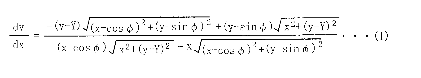
- the angle ⁇ formed by the straight line connecting the intersection point O between the concave mirror 43 and the central axis 7 and each light emitting point 1a with respect to the X axis is not 0 degree, but is set to, for example, 10 to 45 degrees. .
- Each light emitting point 1a may be set on the negative side of the Y axis, and the angle ⁇ may be set negative.
- the curve on the XY plane of the reflecting surface of the concave mirror 43 is expressed by Equation (1) in Expression 1.
- the positions on the XY axes of the light emitting points 1a and the condensing points 9 are S (cos ⁇ , sin ⁇ ) and F (Y, 0).
- Other configurations are the same as those in FIG.
- This curve is an elliptical arc passing through the point O with the points S and F as two focal points.
- the mirror curved surface is a curved surface obtained by rotating this curve on the XY plane around the axis of symmetry C by a certain angle.
- FIG. 7 is a diagram showing a third embodiment of the concave mirror 43 of FIG. 4B.
- the concave mirror 43 is a multilayer mirror, and the shape of the reflecting surface thereof is formed so that the incident angle and the reflecting angle with respect to the normal to the reflecting surface coincide with each other and are symmetrical with respect to the symmetry axis C. .
- the distance from the origin O to each light emitting point 1a (the radius R of the circle centering on the central axis 7) and the distance to the condensing point 9 are set equal.
- the curve on the XY axis of the reflecting surface of the concave mirror 43 is expressed by Expression (2) of Formula 2.
- Other configurations are the same as those in FIG.
- the plasma light 8 can be condensed at the condensing point 9 symmetrically with respect to the optical axis.
- the irradiation angle of the plasma light 8 from the condensing point 9 is the same as the irradiation angle of the plasma light 8 from the light emitting point 1a.
- Other effects are the same as in FIG.
- FIG. 8A and 8B are views of a third embodiment of the plasma light source system according to the present invention.
- FIG. 8A is a plan view and FIG. 8B is a side view.
- the plasma light source system of the present invention includes a plurality (four in this example) of plasma light sources 10 (in this example, 10A, 10B, 10C, 10D) and a condensing device 40.
- the light collecting device 40 has a single rotating body 48, a single rotating device 44, and a single light collecting mirror 46.
- the rotating body 48 installs a plurality of (four) light emitting points 1 a of the plasma light source 10 on the same circumference centered on a single central axis 7.
- the rotating device 44 rotates the rotating body 48 around the central axis 7 so that the light emission point 1a of each plasma light source 10 is located at the same position (the right light emission point 1a in the drawing) when each plasma light source 10 emits light.
- the condensing mirror 46 condenses the plasma light 8 from the same position (the light emitting point 1a on the right side in the figure) toward the condensing point 9.
- the discharge environment holding device 20 and the voltage application device 30 constituting the plasma light source 10 are preferably provided in each of the plurality of plasma light sources 10, but some or all of them may be shared. Other configurations are the same as those of the first embodiment.
- a plurality of plasma light sources 10 are installed on the same circumference, rotated, and at the timing when each plasma light source 10 reaches a position facing the condenser mirror 46.
- the plurality of plasma light sources 10 that periodically emit the plasma light 8 at the predetermined light emitting point 1a are provided.
- the output of the generated plasma light can be greatly increased while suppressing the load.
- the condensing device 40 that condenses the plasma light 8 at the plurality of light emitting points 1a of the plasma light source 10 to the single condensing point 9 is provided, the plasma is emitted from the single condensing point 9 as the EUV light source for lithography. Light can be emitted periodically.
Landscapes
- Physics & Mathematics (AREA)
- Engineering & Computer Science (AREA)
- Plasma & Fusion (AREA)
- General Physics & Mathematics (AREA)
- Optics & Photonics (AREA)
- Exposure Of Semiconductors, Excluding Electron Or Ion Beam Exposure (AREA)
- Exposure And Positioning Against Photoresist Photosensitive Materials (AREA)
- Condensed Matter Physics & Semiconductors (AREA)
- Manufacturing & Machinery (AREA)
- Computer Hardware Design (AREA)
- Microelectronics & Electronic Packaging (AREA)
- Power Engineering (AREA)
- X-Ray Techniques (AREA)
Abstract
Description
前記プラズマ光源の複数の発光点におけるプラズマ光を単一の集光点に集光する集光装置と、を備えたことを特徴とするプラズマ光源システムが提供される。
前記集光装置は、前記中心軸上に位置し前記発光点からのプラズマ光を前記集光点に向けて反射する反射ミラーと、
前記反射ミラーを各プラズマ光源の発光時に該プラズマ光源に向くように、前記中心軸を中心に回転させる回転装置と、を有する。
該集光ミラーと反射ミラーにより、各発光点におけるプラズマ光を単一の集光点に集光する。
各プラズマ光源の発光時に該プラズマ光源の発光点が同一位置に位置するように、前記回転体を前記中心軸を中心に回転させる回転装置と、を有する。
1対の同軸状電極11は、対称面1を中心として対向配置されている。各同軸状電極11は、棒状の中心電極12、管状のガイド電極14及びリング状の絶縁体16からなる。
管状のガイド電極14は、中心電極12を一定の間隔を隔てて囲み、その間にプラズマ媒体を保有するようになっている。プラズマ媒体は、例えばXe,Sn,Li等のガスである。
リング状の絶縁体16は、中心電極12とガイド電極14の間に位置する中空円筒形状の電気的絶縁体であり、中心電極12とガイド電極14の間を電気的に絶縁する。
正電圧源32は、一方(この例では左側)の同軸状電極11の中心電極12にそのガイド電極14より高い正の放電電圧を印加する。
負電圧源34は、他方(この例では右側)の同軸状電極11の中心電極12にそのガイド電極14より低い負の放電電圧を印加する。
トリガスイッチ36は、正電圧源32と負電圧源34を同時に作動させて、それぞれの同軸状電極12に同時に正負の放電電圧を印加する。
この構成により、本発明のプラズマ光源は、1対の同軸状電極11間に管状放電を形成してプラズマを軸方向に封じ込めるようになっている。
以下、この図を参照して、プラズマ光発生方法を説明する。
なおこの際、左側の同軸状電極11の中心電極12は正電圧(+)、ガイド電極14は負電圧(-)に印加され、右側の同軸状電極11の中心電極12は負電圧(-)、そのガイド電極14は正電圧(+)に印加されている。
この管状放電4が形成されると、図に符号5で示すプラズマ閉込め磁場(磁気ビン)が形成され、プラズマ3を半径方向及び軸方向に封じ込むことができる。
すなわち、磁気ビン5はプラズマ3の圧力により中央部は大きくその両側が小さくなり、プラズマ3に向かう軸方向の磁気圧勾配が形成され、この磁気圧勾配によりプラズマ3は中間位置に拘束される。さらにプラズマ電流の自己磁場によって中心方向にプラズマ3は圧縮(Zピンチ)され、半径方向にも自己磁場による拘束が働く。
この状態において、プラズマ3の発光エネルギーに相当するエネルギーを電圧印加装置30から供給し続ければ、高いエネルギー変換効率で、プラズマ光8(EUV)を長時間安定して発生させることができる。
そのため、リソグラフィ光源に要求されるプラズマ光の出力(例えば1kW)を達成するために、光源部に投入する電力を大幅に高めると、熱負荷が過大となり、電極の消耗が激しくなり、装置の寿命が短縮する可能性がある。
この図において、本発明のプラズマ光源システムは、複数(この例では4つ)のプラズマ光源10(この例では、10A,10B,10C,10D)と、集光装置40を備える。
また、各プラズマ光源10は、図1に示したように対向配置された1対の同軸状電極11と、同軸状電極11内にプラズマ媒体を供給しかつプラズマ発生に適した温度及び圧力に保持する放電環境保持装置20と、各同軸状電極11に極性を反転させた放電電圧を印加する電圧印加装置30とを備え、1対の同軸状電極11の間に管状放電を形成してプラズマを軸方向に封じ込めるようになっている。
また、この例において、集光装置40は、単一の反射ミラー42、単一の回転装置44、および複数(この例では4つ)の集光ミラー46(この例では、46A,46B,46C,46D)を有する。
また、集光ミラー46と反射ミラー42は、この両者により、各発光点1aにおけるプラズマ光8を単一の集光点9に集光するように、形状が設定されている。
例えば、図3における中心軸7を中心とする円の半径をR、回転速度をN、プラズマ光8のパルス幅をτとした場合、放電中のプラズマ移動量Δは、2πR・N・τで表され、Nが100(10ヘッド、1kHz)、τが5μs、Rが5cmの場合、プラズマ移動量Δは、約160μmであり、EUVプラズマ光源に適用可能な微小サイズにできる。
その他の構成は、第1実施形態と同様である。
図5において、複数の発光点1aを含む平面と中心軸7との交点を原点Oとし、原点Oと発光点1aを結ぶ線をX軸、原点Oと中心軸7上に位置する集光点9を結ぶ線をY軸、発光点1aと集光点9を結ぶ線を対称軸Cとする。
従って、円周上に配置された個々のプラズマ光源10の発光タイミングと同期して、凹面ミラー43の反射面がそのプラズマ光源10に対面するように回転させることにより、単一の集光点9から高出力、かつ微小サイズのプラズマ光8を周期的に発光させることができる。
これに対し、図5の構成では、単一の凹面ミラー43による1回の反射でプラズマ光8を集光点9に集光するので、反射効率を高くでき、発生したEUV光の利用効率を大きくできる。
図6において、凹面ミラー43は多層膜ミラーであり、その反射面の形状は、反射面に対する法線に対する入射角と反射角が一致し、かつ対称軸Cに対して線対称に形成されている。またこの例では、凹面ミラー43と中心軸7との交点Oと各発光点1aとを結ぶ直線がX軸に対してなす角度φは0度ではなく、例えば10~45度に設定されている。なお、各発光点1aをY軸の負側に設定し、角度φを負に設定してもよい。
この場合、凹面ミラー43の反射面のX-Y平面上の曲線は、数1の式(1)で表される。ここで、各発光点1aと集光点9のX-Y軸上の位置をS(cosφ、sinφ)とF(Y、0)とする。
その他の構成は、図5と同様である。
この曲線は、点S、Fを2つの焦点とし、点Oを通る楕円弧となる。
ミラー曲面は、X-Y平面上のこの曲線を対称軸Cの周りに一定角度回転して得られる曲面である。
その他の効果は、図5と同様である。
図7において、凹面ミラー43は多層膜ミラーであり、その反射面の形状は、反射面に対する法線に対する入射角と反射角が一致し、かつ対称軸Cに対して線対称に形成されている。またこの例では、原点Oから各発光点1aまでの距離(中心軸7を中心とする円の半径R)と集光点9までの距離が等しく設定されている。
この場合、凹面ミラー43の反射面のX-Y軸上の曲線は、数2の式(2)で表される。
その他の構成は、図5と同様である。

その他の効果は、図5と同様である。
この図において、本発明のプラズマ光源システムは、複数(この例では4つ)のプラズマ光源10(この例では、10A,10B,10C,10D)と、集光装置40を備える。
回転体48は、プラズマ光源10の複数(4つ)の発光点1aを、単一の中心軸7を中心とする同一の円周上に設置する。
回転装置44は、各プラズマ光源10の発光時にそのプラズマ光源の発光点1aが同一位置(図で右側の発光点1a)に位置するように、回転体48を中心軸7を中心に回転させる。
その他の構成は、第1実施形態と同様である。
2 面状放電(電流シート)、3 プラズマ、
4 管状放電、5 プラズマ閉込め磁場、
6 プラズマ媒体、7 中心軸、
8 プラズマ光(EUV)、9 集光点、
10(10A,10B,10C,10D) プラズマ光源、
11 同軸状電極、12 中心電極、12a 凹穴、
14 ガイド電極、14a 開口、
16 絶縁体(多孔質セラミック)、
18 プラズマ媒体供給装置、18a リザーバー(ルツボ)、
18b 加熱装置、20 放電環境保持装置、
30 電圧印加装置、32 正電圧源、
34 負電圧源、36 トリガスイッチ、
40 集光装置、42 反射ミラー、43 凹面ミラー、
46(46A,46B,46C,46D) 集光ミラー、
48 回転体
Claims (8)
- 所定の発光点でプラズマ光を周期的に発光する複数のプラズマ光源と、
前記プラズマ光源の複数の発光点におけるプラズマ光を単一の集光点に集光する集光装置と、を備えたことを特徴とするプラズマ光源システム。 - 前記プラズマ光源の複数の発光点は、単一の中心軸を中心とする同一の円周上に設置されており、
前記集光装置は、前記中心軸上に位置し前記発光点からのプラズマ光を前記集光点に向けて反射する反射ミラーと、
前記反射ミラーを各プラズマ光源の発光時に該プラズマ光源に向くように、前記中心軸を中心に回転させる回転装置と、を有することを特徴とする請求項1に記載のプラズマ光源システム。 - 前記集光装置は、前記各発光点のプラズマ光を前記反射ミラーに向けて集光する複数の集光ミラーを有し、
該集光ミラーと反射ミラーにより、各発光点におけるプラズマ光を単一の集光点に集光する、ことを特徴とする請求項2に記載のプラズマ光源システム。 - 前記集光点は、前記中心軸上に位置しており、
前記反射ミラーは、前記発光点からのプラズマ光を前記集光点に向けて集光する凹面ミラーである、ことを特徴とする請求項2に記載のプラズマ光源システム。 - 前記複数の発光点を含む平面と前記中心軸との交点から、各発光点までの距離と前記集光点までの距離が等しく設定されている、ことを特徴とする請求項4に記載のプラズマ光源システム。
- 前記集光装置は、前記プラズマ光源の複数の発光点を、単一の中心軸を中心とする同一の円周上に設置する回転体と、
各プラズマ光源の発光時に該プラズマ光源の発光点が同一位置に位置するように、前記回転体を前記中心軸を中心に回転させる回転装置と、を有することを特徴とする請求項1に記載のプラズマ光源システム。 - 前記集光装置は、前記同一位置からのプラズマ光を前記集光点に向けて集光する集光ミラーを有する、ことを特徴とする請求項6に記載のプラズマ光源システム。
- 前記各プラズマ光源は、対向配置された1対の同軸状電極と、該同軸状電極内にプラズマ媒体を供給しかつプラズマ発生に適した温度及び圧力に保持する放電環境保持装置と、各同軸状電極に極性を反転させた放電電圧を印加する電圧印加装置と、を備え、
1対の同軸状電極間に管状放電を形成してプラズマを軸方向に封じ込める、ことを特徴とする請求項1に記載のプラズマ光源システム。
Priority Applications (5)
| Application Number | Priority Date | Filing Date | Title |
|---|---|---|---|
| KR1020127004072A KR101370615B1 (ko) | 2009-09-01 | 2010-08-25 | 플라즈마 광원 시스템 |
| CN201080038879.9A CN102484045B (zh) | 2009-09-01 | 2010-08-25 | 等离子体光源系统 |
| EP10813648.2A EP2474997A4 (en) | 2009-09-01 | 2010-08-25 | PLASMA LIGHT SOURCE SYSTEM |
| US13/384,899 US20120161631A1 (en) | 2009-09-01 | 2010-08-25 | Plasma light source system |
| JP2011529878A JPWO2011027699A1 (ja) | 2009-09-01 | 2010-08-25 | プラズマ光源システム |
Applications Claiming Priority (2)
| Application Number | Priority Date | Filing Date | Title |
|---|---|---|---|
| JP2009201848 | 2009-09-01 | ||
| JP2009-201848 | 2009-09-01 |
Publications (1)
| Publication Number | Publication Date |
|---|---|
| WO2011027699A1 true WO2011027699A1 (ja) | 2011-03-10 |
Family
ID=43649238
Family Applications (1)
| Application Number | Title | Priority Date | Filing Date |
|---|---|---|---|
| PCT/JP2010/064386 WO2011027699A1 (ja) | 2009-09-01 | 2010-08-25 | プラズマ光源システム |
Country Status (7)
| Country | Link |
|---|---|
| US (1) | US20120161631A1 (ja) |
| EP (1) | EP2474997A4 (ja) |
| JP (2) | JPWO2011027699A1 (ja) |
| KR (1) | KR101370615B1 (ja) |
| CN (1) | CN102484045B (ja) |
| TW (1) | TWI423734B (ja) |
| WO (1) | WO2011027699A1 (ja) |
Cited By (4)
| Publication number | Priority date | Publication date | Assignee | Title |
|---|---|---|---|---|
| JP2012191040A (ja) * | 2011-03-11 | 2012-10-04 | Ihi Corp | プラズマ光源システム |
| JP2012191113A (ja) * | 2011-03-14 | 2012-10-04 | Ihi Corp | プラズマ光源及びプラズマ光源の製造方法 |
| JP2018097105A (ja) * | 2016-12-12 | 2018-06-21 | 株式会社Ihi | プラズマ光源システム |
| JP2018169544A (ja) * | 2017-03-30 | 2018-11-01 | 株式会社Ihi | プラズマ光源 |
Families Citing this family (5)
| Publication number | Priority date | Publication date | Assignee | Title |
|---|---|---|---|---|
| US8895946B2 (en) * | 2012-02-11 | 2014-11-25 | Media Lario S.R.L. | Source-collector modules for EUV lithography employing a GIC mirror and a LPP source |
| US9723703B2 (en) * | 2014-04-01 | 2017-08-01 | Kla-Tencor Corporation | System and method for transverse pumping of laser-sustained plasma |
| KR102345537B1 (ko) | 2014-12-11 | 2021-12-30 | 삼성전자주식회사 | 플라즈마 광원, 및 그 광원을 포함하는 검사 장치 |
| JP7095236B2 (ja) * | 2017-07-19 | 2022-07-05 | 株式会社Ihi | プラズマ光源システム |
| CN114671599B (zh) * | 2022-03-29 | 2022-11-22 | 锦州佑鑫石英科技有限公司 | 大外径直拉单晶用石英坩埚的制备方法 |
Citations (3)
| Publication number | Priority date | Publication date | Assignee | Title |
|---|---|---|---|---|
| JP2003051398A (ja) * | 2001-08-07 | 2003-02-21 | Nikon Corp | X線発生装置、露光装置、露光方法及びデバイス製造方法 |
| JP2003282424A (ja) * | 2002-03-27 | 2003-10-03 | Ushio Inc | 極端紫外光発生装置 |
| JP2004226244A (ja) | 2003-01-23 | 2004-08-12 | Ushio Inc | 極端紫外光源および半導体露光装置 |
Family Cites Families (17)
| Publication number | Priority date | Publication date | Assignee | Title |
|---|---|---|---|---|
| US6566667B1 (en) * | 1997-05-12 | 2003-05-20 | Cymer, Inc. | Plasma focus light source with improved pulse power system |
| US6438199B1 (en) * | 1998-05-05 | 2002-08-20 | Carl-Zeiss-Stiftung | Illumination system particularly for microlithography |
| JP4332648B2 (ja) * | 1999-04-07 | 2009-09-16 | レーザーテック株式会社 | 光源装置 |
| JP2003288998A (ja) * | 2002-03-27 | 2003-10-10 | Ushio Inc | 極端紫外光源 |
| JP2006501660A (ja) * | 2002-09-30 | 2006-01-12 | カール・ツァイス・エスエムティー・アーゲー | 照明の同定用のセンサを備える波長≦193nm用の照明システム |
| DE10305701B4 (de) * | 2003-02-07 | 2005-10-06 | Xtreme Technologies Gmbh | Anordnung zur Erzeugung von EUV-Strahlung mit hohen Repetitionsraten |
| JP4578901B2 (ja) * | 2004-09-09 | 2010-11-10 | 株式会社小松製作所 | 極端紫外光源装置 |
| TW200613706A (en) * | 2004-09-29 | 2006-05-01 | Ushio Electric Inc | EUV generator |
| JP2006156857A (ja) * | 2004-12-01 | 2006-06-15 | Canon Inc | X線発生装置及び露光装置 |
| DE102005030304B4 (de) * | 2005-06-27 | 2008-06-26 | Xtreme Technologies Gmbh | Vorrichtung und Verfahren zur Erzeugung von extrem ultravioletter Strahlung |
| DE102005041567B4 (de) * | 2005-08-30 | 2009-03-05 | Xtreme Technologies Gmbh | EUV-Strahlungsquelle mit hoher Strahlungsleistung auf Basis einer Gasentladung |
| DE102006003683B3 (de) * | 2006-01-24 | 2007-09-13 | Xtreme Technologies Gmbh | Anordnung und Verfahren zur Erzeugung von EUV-Strahlung hoher Durchschnittsleistung |
| JP4884152B2 (ja) * | 2006-09-27 | 2012-02-29 | 株式会社小松製作所 | 極端紫外光源装置 |
| JP5075389B2 (ja) * | 2006-10-16 | 2012-11-21 | ギガフォトン株式会社 | 極端紫外光源装置 |
| US7709816B2 (en) * | 2007-08-16 | 2010-05-04 | Sematech, Inc. | Systems and methods for monitoring and controlling the operation of extreme ultraviolet (EUV) light sources used in semiconductor fabrication |
| US8399867B2 (en) * | 2008-09-29 | 2013-03-19 | Gigaphoton Inc. | Extreme ultraviolet light source apparatus |
| US20100176312A1 (en) * | 2009-01-13 | 2010-07-15 | Hiroshi Komori | Extreme ultra violet light source apparatus |
-
2010
- 2010-08-25 KR KR1020127004072A patent/KR101370615B1/ko not_active IP Right Cessation
- 2010-08-25 WO PCT/JP2010/064386 patent/WO2011027699A1/ja active Application Filing
- 2010-08-25 JP JP2011529878A patent/JPWO2011027699A1/ja active Pending
- 2010-08-25 EP EP10813648.2A patent/EP2474997A4/en not_active Withdrawn
- 2010-08-25 US US13/384,899 patent/US20120161631A1/en not_active Abandoned
- 2010-08-25 CN CN201080038879.9A patent/CN102484045B/zh not_active Expired - Fee Related
- 2010-08-31 TW TW099129226A patent/TWI423734B/zh not_active IP Right Cessation
-
2012
- 2012-07-27 JP JP2012167068A patent/JP2012212942A/ja active Pending
Patent Citations (3)
| Publication number | Priority date | Publication date | Assignee | Title |
|---|---|---|---|---|
| JP2003051398A (ja) * | 2001-08-07 | 2003-02-21 | Nikon Corp | X線発生装置、露光装置、露光方法及びデバイス製造方法 |
| JP2003282424A (ja) * | 2002-03-27 | 2003-10-03 | Ushio Inc | 極端紫外光発生装置 |
| JP2004226244A (ja) | 2003-01-23 | 2004-08-12 | Ushio Inc | 極端紫外光源および半導体露光装置 |
Non-Patent Citations (3)
| Title |
|---|
| HIROTO SATO ET AL.: "Discharge-Produced Plasma EUV Source for Microlithography", OQD-08-28 |
| JEROEN JONKERS: "High power extreme ultraviolet (EUV) light sources for future lithography", PLASMA SOURCES SCIENCE AND TECHNOLOGY, vol. 15, 2006, pages S8 - S16 |
| See also references of EP2474997A4 * |
Cited By (4)
| Publication number | Priority date | Publication date | Assignee | Title |
|---|---|---|---|---|
| JP2012191040A (ja) * | 2011-03-11 | 2012-10-04 | Ihi Corp | プラズマ光源システム |
| JP2012191113A (ja) * | 2011-03-14 | 2012-10-04 | Ihi Corp | プラズマ光源及びプラズマ光源の製造方法 |
| JP2018097105A (ja) * | 2016-12-12 | 2018-06-21 | 株式会社Ihi | プラズマ光源システム |
| JP2018169544A (ja) * | 2017-03-30 | 2018-11-01 | 株式会社Ihi | プラズマ光源 |
Also Published As
| Publication number | Publication date |
|---|---|
| KR101370615B1 (ko) | 2014-03-06 |
| KR20120034124A (ko) | 2012-04-09 |
| JPWO2011027699A1 (ja) | 2013-02-04 |
| CN102484045A (zh) | 2012-05-30 |
| TWI423734B (zh) | 2014-01-11 |
| JP2012212942A (ja) | 2012-11-01 |
| EP2474997A4 (en) | 2014-01-15 |
| TW201130387A (en) | 2011-09-01 |
| CN102484045B (zh) | 2014-12-17 |
| EP2474997A1 (en) | 2012-07-11 |
| US20120161631A1 (en) | 2012-06-28 |
Similar Documents
| Publication | Publication Date | Title |
|---|---|---|
| WO2011027699A1 (ja) | プラズマ光源システム | |
| JP5479723B2 (ja) | プラズマ光源とプラズマ光発生方法 | |
| WO2011027737A1 (ja) | プラズマ光源 | |
| JP5212917B2 (ja) | プラズマ光源 | |
| JP2010123714A (ja) | 極端紫外光光源装置 | |
| JP5622081B2 (ja) | プラズマ光源 | |
| JP5212918B2 (ja) | プラズマ光源 | |
| JP5590305B2 (ja) | プラズマ光源とプラズマ光発生方法 | |
| JP5656014B2 (ja) | プラズマ光源とプラズマ光発生方法 | |
| US10088761B1 (en) | Lithography device and apparatus and method for lithography device | |
| JP5510722B2 (ja) | プラズマ光源とプラズマ光発生方法 | |
| JP5733687B2 (ja) | プラズマ光源の製造方法 | |
| JP5757112B2 (ja) | プラズマ光源の製造方法 | |
| JP5622026B2 (ja) | プラズマ光源とプラズマ光発生方法 | |
| JP5659543B2 (ja) | プラズマ光源とプラズマ光発生方法 | |
| JP5621979B2 (ja) | プラズマ光源とプラズマ光発生方法 | |
| JP5953735B2 (ja) | プラズマ光源 | |
| JP2012191040A (ja) | プラズマ光源システム | |
| JP5948810B2 (ja) | プラズマ光源 | |
| JP7095236B2 (ja) | プラズマ光源システム | |
| JP5552872B2 (ja) | プラズマ光源とプラズマ光発生方法 |
Legal Events
| Date | Code | Title | Description |
|---|---|---|---|
| WWE | Wipo information: entry into national phase |
Ref document number: 201080038879.9 Country of ref document: CN |
|
| WWE | Wipo information: entry into national phase |
Ref document number: 2010813648 Country of ref document: EP |
|
| 121 | Ep: the epo has been informed by wipo that ep was designated in this application |
Ref document number: 10813648 Country of ref document: EP Kind code of ref document: A1 |
|
| ENP | Entry into the national phase |
Ref document number: 2011529878 Country of ref document: JP Kind code of ref document: A |
|
| WWE | Wipo information: entry into national phase |
Ref document number: 13384899 Country of ref document: US |
|
| ENP | Entry into the national phase |
Ref document number: 20127004072 Country of ref document: KR Kind code of ref document: A |
|
| NENP | Non-entry into the national phase |
Ref country code: DE |