WO2011016337A1 - 金属微細構造体のパターン倒壊抑制用処理液及びこれを用いた金属微細構造体の製造方法 - Google Patents
金属微細構造体のパターン倒壊抑制用処理液及びこれを用いた金属微細構造体の製造方法 Download PDFInfo
- Publication number
- WO2011016337A1 WO2011016337A1 PCT/JP2010/062273 JP2010062273W WO2011016337A1 WO 2011016337 A1 WO2011016337 A1 WO 2011016337A1 JP 2010062273 W JP2010062273 W JP 2010062273W WO 2011016337 A1 WO2011016337 A1 WO 2011016337A1
- Authority
- WO
- WIPO (PCT)
- Prior art keywords
- metal
- treatment liquid
- phosphate ester
- collapse
- group
- Prior art date
- Legal status (The legal status is an assumption and is not a legal conclusion. Google has not performed a legal analysis and makes no representation as to the accuracy of the status listed.)
- Ceased
Links
Images

Classifications
-
- H—ELECTRICITY
- H10—SEMICONDUCTOR DEVICES; ELECTRIC SOLID-STATE DEVICES NOT OTHERWISE PROVIDED FOR
- H10P—GENERIC PROCESSES OR APPARATUS FOR THE MANUFACTURE OR TREATMENT OF DEVICES COVERED BY CLASS H10
- H10P70/00—Cleaning of wafers, substrates or parts of devices
- H10P70/20—Cleaning during device manufacture
-
- G—PHYSICS
- G03—PHOTOGRAPHY; CINEMATOGRAPHY; ANALOGOUS TECHNIQUES USING WAVES OTHER THAN OPTICAL WAVES; ELECTROGRAPHY; HOLOGRAPHY
- G03F—PHOTOMECHANICAL PRODUCTION OF TEXTURED OR PATTERNED SURFACES, e.g. FOR PRINTING, FOR PROCESSING OF SEMICONDUCTOR DEVICES; MATERIALS THEREFOR; ORIGINALS THEREFOR; APPARATUS SPECIALLY ADAPTED THEREFOR
- G03F7/00—Photomechanical, e.g. photolithographic, production of textured or patterned surfaces, e.g. printing surfaces; Materials therefor, e.g. comprising photoresists; Apparatus specially adapted therefor
- G03F7/26—Processing photosensitive materials; Apparatus therefor
- G03F7/30—Imagewise removal using liquid means
- G03F7/32—Liquid compositions therefor, e.g. developers
- G03F7/325—Non-aqueous compositions
-
- B—PERFORMING OPERATIONS; TRANSPORTING
- B81—MICROSTRUCTURAL TECHNOLOGY
- B81C—PROCESSES OR APPARATUS SPECIALLY ADAPTED FOR THE MANUFACTURE OR TREATMENT OF MICROSTRUCTURAL DEVICES OR SYSTEMS
- B81C1/00—Manufacture or treatment of devices or systems in or on a substrate
- B81C1/00912—Treatments or methods for avoiding stiction of flexible or moving parts of MEMS
- B81C1/0092—For avoiding stiction during the manufacturing process of the device, e.g. during wet etching
- B81C1/00928—Eliminating or avoiding remaining moisture after the wet etch release of the movable structure
-
- H—ELECTRICITY
- H10—SEMICONDUCTOR DEVICES; ELECTRIC SOLID-STATE DEVICES NOT OTHERWISE PROVIDED FOR
- H10P—GENERIC PROCESSES OR APPARATUS FOR THE MANUFACTURE OR TREATMENT OF DEVICES COVERED BY CLASS H10
- H10P76/00—Manufacture or treatment of masks on semiconductor bodies, e.g. by lithography or photolithography
- H10P76/20—Manufacture or treatment of masks on semiconductor bodies, e.g. by lithography or photolithography of masks comprising organic materials
- H10P76/204—Manufacture or treatment of masks on semiconductor bodies, e.g. by lithography or photolithography of masks comprising organic materials of organic photoresist masks
- H10P76/2041—Photolithographic processes
Definitions
- the present invention relates to a processing solution for suppressing pattern collapse of a metal microstructure and a method for producing a metal microstructure using the same.
- a photolithography technique is used as a method for forming and processing an element having a fine structure used in a wide field such as a semiconductor device or a circuit board.
- a wide field such as a semiconductor device or a circuit board.
- miniaturization, high integration, and high speed of semiconductor devices and the like have advanced remarkably, and the resist pattern used for photolithography has become finer and the aspect ratio has been increasing. I'm following.
- the miniaturization or the like progresses, the collapse of the resist pattern becomes a big problem.
- the collapse of the resist pattern is caused by the surface tension of the processing solution when the processing solution used in the wet processing (mainly rinsing processing for washing away the developing solution) after developing the resist pattern is dried from the resist pattern. It is known that it is generated by the action of stress. Therefore, in order to solve the collapse of the resist pattern, a method of drying by replacing the cleaning liquid with a low surface tension liquid using a nonionic surfactant, an alcohol solvent-soluble compound or the like (for example, Patent Documents 1 and 2). And a method of hydrophobizing the surface of the resist pattern (for example, see Patent Document 3).
- a fine structure made of metal, metal nitride, metal oxide or the like formed by photolithography technology hereinafter referred to as a metal fine structure.
- a metal, metal nitride, or metal oxide is simply included.
- the strength of the metal itself forming the structure is higher than the strength of the resist pattern itself or the bonding strength between the resist pattern and the substrate. Collapse is unlikely to occur.
- semiconductor devices and micromachines become more compact, highly integrated, and faster, the pattern of the structure becomes finer, and the collapse of the pattern of the structure due to an increase in aspect ratio becomes a big problem. come.
- the resist pattern which is an organic material
- the surface state of the metal microstructure are completely different, unlike the case of the collapse of the resist pattern described above, no effective countermeasures can be found, so miniaturization and high integration of semiconductor devices and micromachines.
- the pattern design freedom is significantly hindered, for example, by designing the pattern so that the pattern does not collapse.
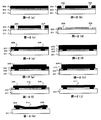
- FIG. 3 is a schematic cross-sectional view for each production stage of metal microstructures produced in Examples 1 to 48 and Comparative Examples 1 to 30.
- FIG. 6 is a schematic cross-sectional view for each production stage of metal microstructures produced in Examples 49 to 112 and Comparative Examples 31 to 70.
- Photoresist 102 Silicon oxide 103. Silicon nitride 104. Silicon substrate 105. Circular opening 106. Cylindrical hole 107. Metal (titanium nitride, tungsten or tantalum) 108. 201. Cylinder of metal (titanium nitride, tungsten or tantalum) Silicon oxide layer 202. Polysilicon 203. Photoresist 204. Prismatic opening 205. Prismatic hole 205 206. Metal (titanium, aluminum oxide, hafnium oxide or ruthenium) prism 207. Metal (titanium, aluminum oxide, hafnium oxide or ruthenium) layer 208. Photoresist 209. Rectangular photomask 210. Metal (titanium, aluminum oxide, hafnium oxide or ruthenium) plate 211. Bridge structure
- the present invention has been made under such circumstances, and provides a treatment liquid capable of suppressing pattern collapse of a metal microstructure such as a semiconductor device or a micromachine, and a method of manufacturing a metal microstructure using the same. It is the purpose.
- the present inventors have found that the object can be achieved with a treatment liquid containing a phosphate ester and / or a polyoxyalkylene ether phosphate ester.
- the present invention has been completed based on such findings. That is, the gist of the present invention is as follows.
- the phosphoric acid ester and / or the polyoxyalkylene ether phosphoric acid ester is represented by the following general formula (1) and / or general formula (2): [Wherein, R 1 represents an alkyl group having 2 to 24 carbon atoms and an alkenyl group having 2 to 24 carbon atoms, R 2 represents an alkanediyl group or alkenediyl group having 2 to 6 carbon atoms, and a plurality of R 1 and R 2 may be the same or different.
- N represents a number from 0 to 20, and a plurality of n may be the same or different.
- the treatment liquid according to 1 above which is represented by [3] The processing liquid according to the above 1 or 2, further comprising water.
- OR 2 in the general formulas (1) and (2) is an oxyethylene group and / or an oxypropylene group.
- the pattern of the metal microstructure is titanium nitride, titanium, ruthenium, ruthenium oxide, tungsten, tungsten silicide, tungsten nitride, aluminum oxide, hafnium oxide, hafnium silicate, hafnium silicate, platinum, tantalum, tantalum oxide, nitride 6.
- the pattern of the metal microstructure is titanium nitride, titanium, ruthenium, ruthenium oxide, tungsten, tungsten silicide, tungsten nitride, aluminum oxide, hafnium oxide, hafnium silicate, hafnium silicate, platinum, tantalum, tantalum oxide, nitride 8.
- the metal microstructure is a semiconductor device or a micromachine.
- a treatment liquid capable of suppressing pattern collapse of a metal microstructure such as a semiconductor device or a micromachine, and a method of manufacturing a metal microstructure using the same.
- the treatment liquid of the present invention is used for suppressing pattern collapse of a metal microstructure and contains a phosphate ester and / or a polyoxyalkylene ether phosphate ester.
- the phosphate ester and polyoxyalkylene ether phosphate ester used in the treatment liquid of the present invention are considered to adsorb the metal material used for the pattern of the metal microstructure and hydrophobize the surface of the pattern. .
- “hydrophobization” means that the contact angle between the surface of a metal treated with the treatment liquid of the present invention and water becomes 70 ° or more.
- the phosphate ester and the polyoxyalkylene ether phosphate ester usually contain a monoester and a diester at the same time, but the monoester or diester can also be used alone.
- Preferred examples of the phosphate ester and polyoxyalkylene ether phosphate ester are those represented by the following general formula (1) and / or (2).
- R 1 represents an alkyl group having 2 to 24 carbon atoms and an alkenyl group having 2 to 24 carbon atoms.
- an alkyl group having 6 to 18 carbon atoms is preferable, an alkyl group having 12 to 18 carbon atoms is more preferable, an alkyl group having 12, 13, or 18 carbon atoms is further preferable, and an alkyl group having 18 carbon atoms is particularly preferable. It is a group.
- the alkyl group may be linear, branched or cyclic, and may have a halogen atom or a substituent, such as an n-hexyl group, 1-methylhexyl group, 2-methyl group.
- Hexyl group 1-pentylhexyl group, cyclohexyl group, 1-hydroxyhexyl group, 1-chlorohexyl group, 1,3-dichlorohexyl group, 1-aminohexyl group, 1-cyanohexyl group, 1-nitrohexyl group
- various heptyl groups various octyl groups, various nonyl groups, various decyl groups, various undecyl groups, various dodecyl groups, various tridecyl groups, various tetradecyl groups, various pentadecyl groups, various hexadecyl groups, various heptadecyl groups, etc.
- the alkenyl group is preferably an alkenyl group having 2 to 24 carbon atoms, more preferably an alkenyl group having 4 to 18 carbon atoms, still more preferably an alkenyl group having 6 to 18 carbon atoms, and particularly preferably an oleyl group having 18 carbon atoms. Further, the alkenyl group may be linear or branched.
- R 2 represents an alkanediyl group or alkenediyl group having 2 to 6 carbon atoms, and a plurality of R 2 may be the same or different.
- the alkanediyl group having 2 to 6 carbon atoms may be linear or branched.
- linear ones such as ethylene group, 1,3-propanediyl group, 1,4-butanediyl group, 1,5-pentanediyl group 1,6-hexanediyl group and the like are preferable, and ethylene and 1,2-propanediyl group are particularly preferable. That is, as OR 2 , an oxyethylene group and an oxypropylene group are particularly preferable.
- n in the formula represents a number from 0 to 20, preferably 0 to 14. If n is within the above range, the phosphate ester and / or polyoxyalkylene ether phosphorus used in the present invention depends on the balance between the functional group represented by R 1 in the formula and the hydrophilic-hydrophobic property. This is because the acid ester is a liquid, and is easily dissolved in a solvent such as water or an organic solvent and is suitably used as a treatment liquid.
- the compounds represented by the general formulas (1) and (2) are alkyl phosphates and polyoxyalkylenes in which R 1 and R 3 are alkyl groups and R 2 is an alkanediyl group, respectively.
- the alkyl ether phosphate ester, R 1 is an alkenyl group
- R 2 is an alkanediyl group, such as an alkenyl phosphate ester and a polyoxyalkylene alkenyl ether phosphate ester, respectively.
- Two R 1 in the compound represented by the general formula (2) may be the same or different. This is because, when the above compound is used, the treatment liquid of the present invention can exhibit more excellent pattern collapse suppressing ability.
- alkyl phosphates such as those in which R 1 has a carbon number of 6 to 10 (hexyl to decyl); polyoxyethylene hexyl ether phosphates (n: 1 to 8), polyoxy Ethylene heptyl ether phosphate (n: 1 to 8), polyoxyethylene octyl ether phosphate (n: 1 to 8), polyoxyethylene nonenyl ether phosphate (n: 1 to 8), polyoxyethylene Decyl ether phosphate (n: 1 to 12), polyoxyethylene lauryl ether phosphate (n: To 12), polyoxyethylene tridecyl ether phosphate esters (n: 1 to 12), polyoxyethylene stearyl ether phosphate esters (n: 1 to 12)
- the treatment liquid of the present invention preferably further contains water and is preferably an aqueous solution.
- the water is preferably water from which metal ions, organic impurities, particle particles, and the like have been removed by distillation, ion exchange treatment, filter treatment, various adsorption treatments, and the like, and pure water and ultrapure water are particularly preferred.
- the treatment liquid of the present invention contains the above-described phosphate ester and polyoxyalkylene ether phosphate ester, preferably contains water, and other various additives usually used in the treatment liquid as long as the effects of the treatment liquid are not impaired. Is included.
- the content of the phosphate ester and polyoxyalkylene ether phosphate ester in the treatment liquid of the present invention is preferably 10 ppm to 50%. If the content of the phosphate ester and the polyoxyalkylene ether phosphate ester is within the above range, the effects of these compounds can be sufficiently obtained.
- the treatment liquid of the present invention is suitably used for suppressing pattern collapse of a metal microstructure such as a semiconductor device or a micromachine.
- a metal microstructure such as a semiconductor device or a micromachine.
- Titanium nitride Ti (chi Emissions), Ru (ruthenium), RuO (ruthenium oxide), SrRuO 3 (SRO), W ( tungsten), WSi (tungsten silicide), Al 2 O 3 (aluminum oxide), HfO 2 (hafnium oxide), Pt (platinum ), Ta (tantalum), Ta 2 O 5 (tantalum oxide), and TaN (tantalum nitride) are more preferable.
- TiN (titanium nitride), W (tungsten), Ta (tantalum), Ti (titanium), Al 2 O 3 (Aluminum oxide) and HfO 2 (hafnium oxide) Ru (ruthenium) are more preferable.
- the metal microstructure is patterned on an insulating film type such as SiO 2 (silicon oxide film) or TEOS (tetraethoxyorthosilane oxide film), or the insulating film type is formed on a part of the metal microstructure. May be included.
- an insulating film type such as SiO 2 (silicon oxide film) or TEOS (tetraethoxyorthosilane oxide film)
- the insulating film type is formed on a part of the metal microstructure. May be included.
- the treatment liquid of the present invention exhibits an excellent effect of suppressing pattern collapse on not only a conventional metal microstructure but also a metal microstructure having a finer and higher aspect ratio.
- the aspect ratio is a value calculated by (pattern height / pattern width)
- the treatment liquid of the present invention is an excellent pattern for patterns having a high aspect ratio of 3 or more, and further 7 or more.
- the treatment liquid of the present invention has a 1: 1 line-and-space pattern and the interval between patterns even when the pattern size is 300 nm or less, 150 nm or less, 100 nm or less, and even 50 nm or less.
- the metal microstructure manufacturing method of the present invention is characterized by using the above-described treatment liquid of the present invention in a cleaning step after wet etching or dry etching. More specifically, in the cleaning step, preferably, after the metal microstructure pattern and the treatment liquid of the present invention are brought into contact with each other by dipping, spray discharge, spraying, etc., the treatment liquid is replaced with water. dry.
- the immersion time is preferably 10 seconds to 30 minutes, more preferably 15 seconds to 20 minutes, and still more preferably 20 seconds to 15 minutes.
- the temperature condition is preferably 10 to 60 ° C., more preferably 15 to 50 ° C., still more preferably 20 to 40 ° C., and particularly preferably 25 to 40 ° C.
- the surface of the pattern is hydrophobized, whereby the collapse of the pattern can be suppressed.
- the treatment liquid of the present invention includes a wet etching process or a dry etching process in the manufacturing process of the metal microstructure, followed by a wet process (etching or cleaning, rinsing for washing away the cleaning liquid), and then drying. If it has the process to do, it can apply widely irrespective of the kind of metal microstructure. For example, (i) in the manufacture of a DRAM type semiconductor device, after wet etching is performed on an insulating film around a conductive film (see, for example, Japanese Patent Laid-Open Nos.
- a strip After a cleaning step for removing contaminants generated after dry etching or wet etching at the time of processing a gate electrode in the manufacture of a semiconductor device having a transistor having a fin-like shape for example, Japanese Patent Application Laid-Open No.
- Examples 1 to 16 As shown in FIG. 1A, after a silicon nitride 103 (thickness: 100 nm) and a silicon oxide 102 (thickness: 1200 nm) are formed on a silicon substrate 104, a photoresist 101 is formed. By exposing and developing the photoresist 101, a circle-ring opening 105 ( ⁇ 125 nm, distance between the circle and the circle: 50 nm) shown in FIG. 1B is formed, and dry using the photoresist 101 as a mask. A cylindrical hole 106 shown in FIG. 1C was formed in the silicon oxide 102 by etching up to the silicon nitride 103 layer.
- the photoresist 101 was removed by ashing to obtain a structure in which a cylindrical hole 106 reaching the silicon nitride 103 layer was formed in the silicon oxide 102 shown in FIG.
- Titanium nitride is filled and deposited as a metal 107 in the cylindrical hole 106 of the obtained structure (FIG. 1- (e)), and chemical mechanical polishing (CMP) is used to remove excess on the silicon oxide 102.
- CMP chemical mechanical polishing
- the metal (titanium nitride) 107 was removed to obtain a structure in which a metal (titanium nitride) cylinder 108 was embedded in the silicon oxide 102 shown in FIG.
- the silicon oxide 102 of the obtained structure is dissolved and removed with hydrofluoric acid, and then contacted with pure water, treatment solutions 1 to 16, and pure water in that order, and dried, as shown in FIG. A structure was obtained.
- the obtained structure has a microstructure having a cylindrical-chimney pattern ( ⁇ 125 nm, height: 1200 nm (aspect ratio: 9.6), distance between cylinder: 50 nm) of metal (titanium nitride). And 70% or more of the pattern did not collapse.
- pattern collapse was observed using “FE-SEM S-5500 (model number)” manufactured by Hitachi High-Technologies Corporation, and the collapse suppression rate was calculated as the ratio of the pattern that did not collapse in the total number of patterns.
- Example 1 the silicon oxide 102 of the structure shown in FIG. 1 (f) was dissolved and removed with hydrofluoric acid, and then treated with pure water only. ) was obtained. Over 50% of the pattern of the obtained structure caused collapse as shown in FIG. 1 (h) (the collapse inhibition rate is less than 50%).
- Table 3 shows the results of the treatment liquid, the treatment method, and the collapse inhibition rate used in Comparative Example 1.
- Comparative Examples 2-10 In Example 1, the silicon oxide 102 of the structure shown in FIG. 1 (f) was dissolved and removed with hydrofluoric acid and treated with pure water, and then the comparative solutions 1 to 9 shown in Table 2 were used instead of the treating solution 1. Except for treatment in the same manner as in Example 1, the structures shown in FIG. Over 50% of the pattern of the obtained structure collapsed as shown in FIG. 1 (h). The compositions of Comparative Solutions 1 to 9 used in Comparative Examples 2 to 10 are shown in Table 2, and the Comparative Solution used in each Example, the treatment method, and the results of the collapse inhibition rate are shown in Table 3.
- Examples 17-32 In Examples 1 to 16, the structure shown in FIG. 1G of Examples 17 to 32 was obtained in the same manner as Examples 1 to 16, except that tungsten was used as the metal 107 instead of titanium nitride. .
- the resulting structure is a microstructure having a cylindrical pattern of metal (tungsten) cylinder 108 ( ⁇ 125 nm, height: 1200 nm (aspect ratio: 9.6), distance between cylinder: 50 nm). And 70% or more of the pattern did not collapse.
- the compositions of the treatment liquids 1 to 16 used in each example are shown in Table 1, and the treatment liquids used in each example, the treatment method, and the results of the collapse suppression rate are shown in Table 4.
- Comparative Examples 11-20 In Comparative Examples 1 to 10, the structure shown in FIG. 1G of Comparative Examples 11 to 20 was obtained in the same manner as Comparative Examples 1 to 10, except that tungsten was used as the metal 107 instead of titanium nitride. It was. Over 50% of the pattern of the obtained structure collapsed as shown in FIG. 1 (h).
- the composition of Comparative Solutions 1 to 9 used in each example is shown in Table 2, and the results of the Comparative Solution used in each Example, the treatment method, and the collapse inhibition rate are shown in Table 4.
- Examples 33-48 In Examples 1 to 16, the structure shown in FIG. 1 (g) of Examples 33 to 48 was obtained in the same manner as in Examples 1 to 16, except that tantalum was used as the metal 107 instead of titanium nitride. It was. The resulting structure is a microstructure having a cylindrical pattern of metal (tantalum) cylinder 108 ( ⁇ 125 nm, height: 1200 nm (aspect ratio: 9.6), distance between cylinder: 50 nm). And 70% or more of the pattern did not collapse.
- the compositions of the treatment liquids 1 to 16 used in each example are shown in Table 1, and the treatment liquids used in each example, the treatment method, and the results of the collapse suppression rate are shown in Table 5.
- Comparative Examples 21-30 In Comparative Examples 1 to 10, the structure shown in FIG. 1G of Comparative Examples 21 to 30 was obtained in the same manner as Comparative Examples 1 to 10 except that tantalum was used as the metal 107 instead of titanium nitride. It was. Over 50% of the pattern of the obtained structure collapsed as shown in FIG. 1 (h).
- Table 2 shows the compositions of Comparative Solutions 1 to 9 used in each example, and Table 5 shows the results of Comparative Solution, treatment method, and collapse suppression rate used in each Example.
- a polysilicon 202 (thickness: 100 nm) is formed on a silicon oxide layer 201 formed on a silicon substrate, and a photoresist 203 is formed thereon.
- the photoresist 203 is exposed and developed to form a prismatic opening 204 (1000 nm ⁇ 8000 nm) shown in FIG. 2B, and dry etching is performed on the polysilicon 202 by using the photoresist 203 as a mask.
- a prismatic hole 205 shown in (c) was formed by etching up to the silicon oxide layer 201.
- the photoresist 203 was removed by ashing to obtain a structure in which a prismatic hole 205 reaching the silicon oxide layer 201 was opened in the polysilicon 202 shown in FIG.
- the prismatic hole 205 of the obtained structure is filled and deposited with titanium as a metal to form a metal (titanium) prism 206 and a metal (titanium) layer 207 (FIG. 2E).
- a photoresist 208 was formed on the layer 207 (FIG. 2F).
- a rectangular photomask 209 that covers the area including the two metal (titanium) prisms 206 shown in FIG. 2G is formed, and the rectangular photomask 209 is formed.
- the metal (titanium) layer 207 was dry-etched to form a metal (titanium) plate 210 having metal (titanium) prisms 206 at both lower ends shown in FIG. 2 (h). Further, the rectangular photomask 209 was removed by ashing to obtain a structure made of a metal (titanium) plate 210 having polysilicon 202 and metal (titanium) prisms 206 shown in FIG. The obtained structure polysilicon 202 was dissolved and removed with an aqueous tetramethylammonium hydroxide solution, and then contacted in the order of pure water, treatment liquids 1 to 16 and pure water, and then dried, Example 49 A bridge structure 211 shown in FIG.
- the obtained bridge structure 211 has a metal (titanium) plate 210 (length ⁇ width: 15000 nm ⁇ 10000 nm, thickness: 300 nm, aspect ratio: 50) and metal (titanium) prisms (length ⁇ width: 1000 nm ⁇ ) at both ends thereof.
- the metal (titanium) plate 210 of 70% or more did not collapse and the silicon oxide layer 201 was not touched.
- the collapse of the pattern was observed using “FE-SEM S-5500 (model number)” manufactured by Hitachi High-Technologies Corporation.
- Table 1 The compositions of the treatment liquids 1 to 16 used in each example are shown in Table 1, and the treatment liquids used in each example, the treatment method, and the results of the collapse suppression rate are shown in Table 6.
- Example 49 the same procedure as in Example 49 was performed, except that the polysilicon 202 having the structure shown in FIG. 2 (i) was dissolved and removed with a tetramethylammonium hydroxide aqueous solution and then treated with pure water only. A bridge structure 211 shown in FIG. 2J was obtained. More than 50% of the obtained bridge structure 211 had collapsed as shown in FIG. 2 (k). Table 6 shows the results of the treatment liquid, the treatment method, and the collapse inhibition rate used in Comparative Example 31.
- Comparative Examples 32-40 In Example 49, after the polysilicon 202 having the structure shown in FIG. 2 (i) was dissolved and removed with an aqueous tetramethylammonium hydroxide solution and treated with pure water, it is shown in Table 2 instead of the treatment liquid 1.
- a bridge structure 211 shown in FIG. 2 (j) of Comparative Examples 32 to 40 was obtained in the same manner as in Example 49 except that the treatment was performed using Comparative Solutions 1 to 9. More than 50% of the obtained bridge structures 211 had collapsed as shown in FIG. 2 (k) (the collapse inhibition rate was less than 50%).
- the composition of Comparative Solutions 1 to 9 used in Comparative Example 31 is shown in Table 2, and the Comparative Solution used in each Example, the treatment method, and the collapse inhibition rate are shown in Table 6.
- Examples 65-80 In Examples 49 to 64, a bridge structure 211 shown in FIG. 2 (j) of Examples 65 to 80 was obtained in the same manner as Examples 49 to 64 except that aluminum oxide was used instead of titanium. It was.
- the obtained bridge structure 211 is composed of a metal (aluminum oxide) plate 210 (length ⁇ width: 15000 nm ⁇ 10000 nm, thickness: 300 nm, aspect ratio: 50) and metal (aluminum oxide) prisms (length ⁇ width: Although the microstructure has a thickness of 1000 nm ⁇ 8000 nm and height: 100 nm, the metal (aluminum oxide) plate 210 of 70% or more did not collapse and the silicon oxide layer 201 was not touched.
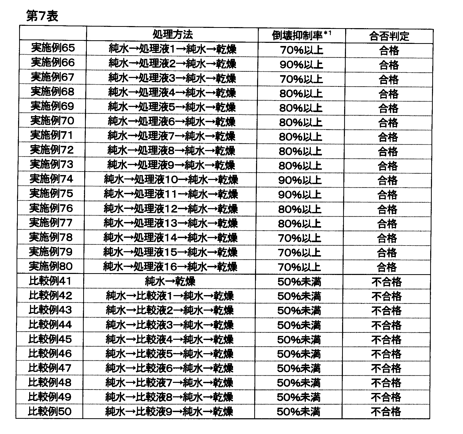
- the compositions of the treatment liquids 1 to 16 used in each example are shown in Table 1, and the treatment liquids used in each example, the treatment method, and the results of the collapse suppression rate are shown in Table 7.
- Comparative Examples 41-50 In Comparative Examples 31 to 40, a bridge structure 211 shown in FIG. 2J of Comparative Examples 41 to 50 is obtained in the same manner as Comparative Examples 31 to 40 except that aluminum oxide is used instead of titanium as a metal. It was. More than 50% of the obtained bridge structures collapsed as shown in Fig. 2 (k).
- Table 2 shows the compositions of Comparative Solutions 1 to 9 used in each example, and Table 7 shows the results of the Comparative Solution, the treatment method, and the collapse inhibition rate used in each Example.
- Examples 81-96 In Examples 49 to 64, a bridge structure 211 shown in FIG. 2J of Examples 81 to 96 was obtained in the same manner as Examples 49 to 64 except that hafnium oxide was used instead of titanium as the metal. It was.
- the obtained bridge structure 211 includes a metal (hafnium oxide) plate 210 (vertical ⁇ horizontal: 15000 nm ⁇ 10000 nm, thickness: 300 nm, aspect ratio: 50) and metal (hafnium oxide) prisms (vertical ⁇ horizontal: both ends).
- the microstructure has a thickness of 1000 nm ⁇ 8000 nm and height: 100 nm, 70% or more of the metal (hafnium oxide) plate 210 is not collapsed and the silicon oxide layer 201 is not touched.
- the compositions of the treatment liquids 1 to 16 used in each example are shown in Table 1, and the treatment liquids, treatment methods, and results of the collapse inhibition rate used in each example are shown in Table 8.
- Comparative Examples 51-60 In Comparative Examples 31 to 40, the bridge structure 211 shown in FIG. 2J of Comparative Examples 51 to 60 was obtained in the same manner as Comparative Examples 31 to 40 except that hafnium oxide was used instead of titanium as the metal. It was. More than 50% of the obtained bridge structures collapsed as shown in Fig. 2 (k).
- the composition of Comparative Solutions 1 to 9 used in each example is shown in Table 2, and the results of the Comparative Solution used in each Example, the treatment method, and the collapse inhibition rate are shown in Table 8.
- Examples 97-112 In Examples 49 to 64, a bridge structure 211 shown in FIG. 2J of Examples 97 to 112 was obtained in the same manner as in Examples 49 to 64 except that ruthenium was used instead of titanium as the metal. .
- the obtained bridge structure 211 includes a metal (ruthenium) plate 210 (length ⁇ width: 15000 nm ⁇ 10000 nm, thickness: 300 nm, aspect ratio: 50) and metal (ruthenium) prisms (length ⁇ width: 1000 nm ⁇ ) at both ends thereof.
- the metal (ruthenium) plate 210 of 70% or more did not collapse, and the silicon oxide layer 201 was not touched.
- Comparative Examples 61-70 In Comparative Examples 31 to 40, a bridge structure 211 shown in FIG. 2J of Comparative Examples 61 to 70 was obtained in the same manner as Comparative Examples 31 to 40 except that ruthenium was used instead of titanium as a metal. . More than 50% of the obtained bridge structures collapsed as shown in Fig. 2 (k).
- Table 2 shows the compositions of Comparative Solutions 1 to 9 used in each example, and Table 9 shows the results of Comparative Solution, treatment method, and collapse suppression rate used in each Example.
- the treatment liquid of the present invention can be suitably used for suppressing pattern collapse in the production of metal microstructures such as semiconductor devices and micromachines (MEMS).
- MEMS micromachines
Landscapes
- Engineering & Computer Science (AREA)
- Manufacturing & Machinery (AREA)
- Microelectronics & Electronic Packaging (AREA)
- Physics & Mathematics (AREA)
- General Physics & Mathematics (AREA)
- Cleaning Or Drying Semiconductors (AREA)
- Exposure Of Semiconductors, Excluding Electron Or Ion Beam Exposure (AREA)
- Weting (AREA)
- Photosensitive Polymer And Photoresist Processing (AREA)
- ing And Chemical Polishing (AREA)
Abstract
Description
102.酸化珪素
103.窒化珪素
104.シリコン基板
105.円状開口部
106.円筒状孔
107.金属(窒化チタン、タングステンまたはタンタル)
108.金属(窒化チタン、タングステンまたはタンタル)の円筒
201.酸化珪素層
202.ポリシリコン
203.フォトレジスト
204.角柱状開口部
205.角柱状孔205
206.金属(チタン、酸化アルミニウム、酸化ハフニウムまたはルテニウム)角柱
207.金属(チタン、酸化アルミニウム、酸化ハフニウムまたはルテニウム)層
208.フォトレジスト
209.長方形型フォトマスク
210.金属(チタン、酸化アルミニウム、酸化ハフニウムまたはルテニウム)板
211.橋梁構造体
本発明は、このような状況下になされたもので、半導体装置やマイクロマシンといった金属微細構造体のパターン倒壊を抑制しうる処理液及びこれを用いた金属微細構造体の製造方法を提供することを目的とするものである。
本発明は、かかる知見に基づいて完成したものである。すなわち、本発明の要旨は下記のとおりである。
[2]リン酸エステル及び/又はポリオキシアルキレンエーテルリン酸エステルが、下記一般式(1)及び/又は一般式(2):
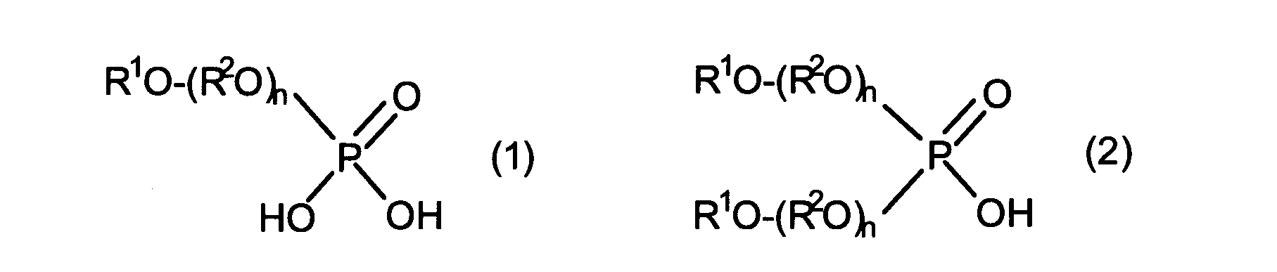
で表されるものである上記1に記載の処理液。
[3]さらに水を含む上記1又は2に記載の処理液。
[4]前記一般式(1)及び(2)におけるOR2が、オキシエチレン基及び/又はオキシプロピレン基である上記1~3のいずれかに記載の処理液。
[5]リン酸エステル及び/又はポリオキシアルキレンエーテルリン酸エステルの含有量が10ppm~50%である上記1~4のいずれかに記載の処理液。
[6]金属微細構造体のパターンが、窒化チタン、チタン、ルテニウム、酸化ルテニウム、タングステン、タングステンシリサイド、窒化タングステン、酸化アルミニウム、酸化ハフニウム、ハフニウムシリケート、窒化ハフニウムシリケート、白金、タンタル、酸化タンタル、窒化タンタル、ニッケルシリサイド、ニッケルシリコンゲルマニウム、ニッケルゲルマニウムから選ばれる少なくとも一種の材料を用いてなるものである上記1~5のいずれかに記載の処理液。
[7]ウェットエッチング又はドライエッチングの後の洗浄工程において、上記1~6のいずれかに記載の処理液を用いることを特徴とする金属微細構造体の製造方法。
[8]金属微細構造体のパターンが、窒化チタン、チタン、ルテニウム、酸化ルテニウム、タングステン、タングステンシリサイド、窒化タングステン、酸化アルミニウム、酸化ハフニウム、ハフニウムシリケート、窒化ハフニウムシリケート、白金、タンタル、酸化タンタル、窒化タンタル、ニッケルシリサイド、ニッケルシリコンゲルマニウム、ニッケルゲルマニウムから選ばれる少なくとも一種の材料を用いてなるものである上記7に記載の製造方法。
[9]金属微細構造体が、半導体装置又はマイクロマシンである上記7又は8に記載の製造方法。
本発明の処理液は、金属微細構造体のパターン倒壊抑制に用いられ、リン酸エステル及び/又はポリオキシアルキレンエーテルリン酸エステルを含むものである。
本発明の処理液に用いられるリン酸エステル及びポリオキシアルキレンエーテルリン酸エステルは、金属微細構造体のパターンに用いられる金属材料と吸着して、該パターンの表面を疎水化しているものと考えられる。本発明において疎水化とは、本発明の処理液にて処理された金属の表面と水との接触角が70°以上となることをいう。リン酸エステル及びポリオキシアルキレンエーテルリン酸エステルは、通常モノエステル及びジエステルを同時に含むものであるが、モノエステル又はジエステルを単独で用いることもできる。リン酸エステル及びポリオキシアルキレンエーテルリン酸エステルとしては、下記一般式(1)及び/又は(2)で表されるものであることが好ましく挙げられる。

炭素数2~6のアルカンジイル基は、直鎖状、枝分かれ状のいずれであってもよく、例えばエチレン基、1,2-プロパンジイル基、1,3-プロパンジイル基、各種ブタンジイル基、各種ペンタンジイル基、各種ヘキサンジイル基などを挙げることができるが、これらの中で直鎖状のもの、例えばエチレン基、1,3-プロパンジイル基、1,4-ブタンジイル基、1,5-ペンタンジイル基、1,6-ヘキサンジイル基などが好ましく挙げられ、特にエチレン、1,2-プロパンジイル基が好ましい、すなわち、OR2としては、オキシエチレン基、オキシプロピレン基が特に好ましい。
本発明の処理液は、さらに水を好ましく含み、水溶液であることが好ましい。水としては、蒸留、イオン交換処理、フィルター処理、各種吸着処理などによって、金属イオンや有機不純物、パーティクル粒子などが除去されたものが好ましく、特に純水、超純水が好ましい。
本発明の処理液は、上記したリン酸エステル及びポリオキシアルキレンエーテルリン酸エステルを含み、好ましくは水を含み、その他、処理液に通常用いられる各種添加剤を処理液の効果を害しない範囲で含むものである。
本発明の処理液中のリン酸エステル及びポリオキシアルキレンエーテルリン酸エステルの含有量は、10ppm~50%であることが好ましい。リン酸エステル及びポリオキシアルキレンエーテルリン酸エステルの含有量が上記範囲内であれば、これらの化合物の効果が十分得られる。さらに、取り扱いやすさや経済性や泡立ちを考慮すると、より低濃度の10%以下で用いることが好ましく、より好ましくは10~2000ppmであり、さらに好ましくは10~1000ppmである。
これらの化合物の水に対する溶解性が十分ではなく相分離するような場合、アルコールなどの有機溶剤を加えてもよいし、酸、アルカリを加えて溶解性を補ってもよい。相分離せず単に白濁した場合でも、その処理液の効果を害しない範囲で用いてもよいし、その処理液が均一となるように撹拌を伴って使用してもよい。また、処理液の白濁を避けるために、上記と同様にアルコールなどの有機溶剤や酸、アルカリを加えてから用いてもよい。
なお、金属微細構造体は、SiO2(シリコン酸化膜)やTEOS(テトラエトキシオルソシラン酸化膜)などの絶縁膜種の上にパターニングされる場合や、金属微細構造の一部に絶縁膜種が含まれる場合がある。
本発明の金属微細構造体の製造方法は、ウェットエッチング又はドライエッチングの後の洗浄工程において、上記した本発明の処理液を用いることを特徴とするものである。より具体的には、該洗浄工程において、好ましくは金属微細構造体のパターンと本発明の処理液とを浸漬、スプレー吐出、噴霧などにより接触させた後、水で該処理液を置換してから乾燥させる。ここで、金属微細構造体のパターンと本発明の処理液とを浸漬により接触させる場合、浸漬時間は10秒~30分が好ましく、より好ましくは15秒~20分、さらに好ましくは20秒~15分、特に好ましくは30秒~10分であり、温度条件は10~60℃が好ましく、より好ましくは15~50℃、さらに好ましくは20~40℃、特に好ましくは25~40℃である。また、金属微細構造体のパターンと本発明の処理液との接触の前に、あらかじめ水で洗浄を行ってもよい。このように、金属微細構造体のパターンと本発明の処理液とを接触させることにより、該パターンの表面上を疎水化することにより、該パターンの倒壊を抑制することが可能となる。
第1表に示される配合組成(質量%)に従い、実施例1及び2金属微細構造体のパターン倒壊抑制用処理液を調合した。
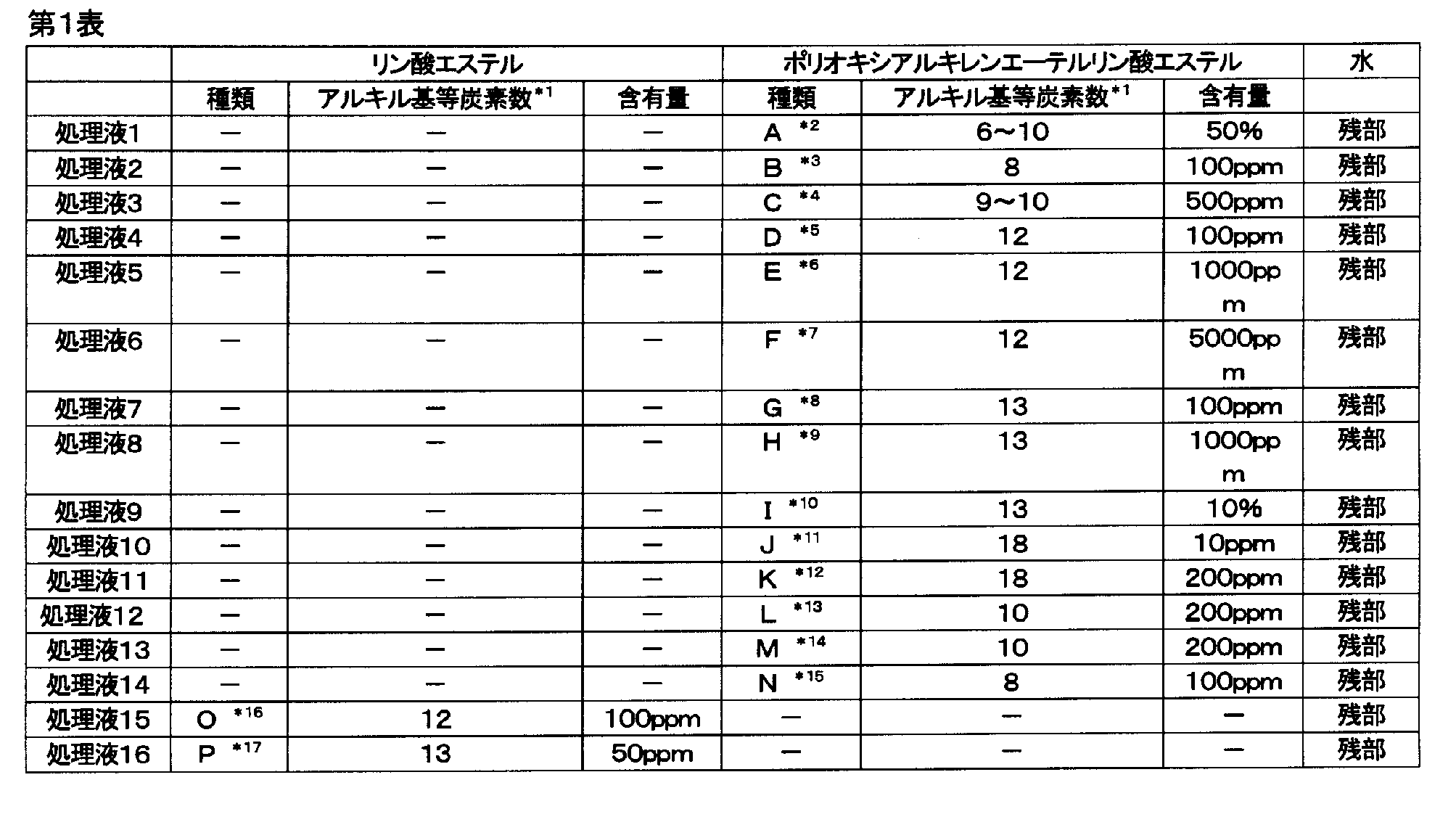
*2,「RA-600(商品名)」,東邦化学工業株式会社製:ポリオキシエチレンアルキルエーテルリン酸エステル(アルキル基が炭素数6~10)の混合物であり、一般式(1)及び(2)におけるn=4)。
*3,「ED-200(商品名)」,東邦化学工業株式会社製:ポリオキシエチレンオクチルエーテルリン酸エステル(一般式(1)及び(2)におけるn=1)である。
*4,ポリオキシエチレンポリオキシプロピレンアルキルエーテルリン酸エステル(アルキル基が炭素数9~11)の混合物であり、一般式(1)及び(2)におけるn=5及び6)。
*5,「ML-220(商品名)」,東邦化学工業株式会社製:ポリオキシエチレンラウリルエーテルリン酸エステルである(一般式(1)及び(2)におけるn=2)。
*6,「RD-510Y(商品名)」,東邦化学工業株式会社製:ポリオキシエチレンラウリルエーテルリン酸エステルである(一般式(1)及び(2)におけるn=4)。
*7,「ML-240(商品名)」,東邦化学工業株式会社製:ポリオキシエチレンラウリルエーテルリン酸エステルである(一般式(1)及び(2)におけるn=4)。
*8,「RS-410(商品名)」,東邦化学工業株式会社製:ポリオキシエチレントリデシルエーテルリン酸エステルである(一般式(1)及び(2)におけるn=3)。
*9,「RS-610(商品名)」,東邦化学工業株式会社製:ポリオキシエチレントリデシルエーテルリン酸エステルである(一般式(1)及び(2)におけるn=6)。
*10,「RS-710(商品名)」,東邦化学工業株式会社製:ポリオキシエチレントリデシルエーテルリン酸エステルである(一般式(1)及び(2)におけるn=10)。
*11,「RB-410(商品名)」,東邦化学工業株式会社製:ポリオキシエチレンステアリルエーテルリン酸エステルである(一般式(1)及び(2)におけるn=4)。
*12,ポリオキシエチレンオレイルエーテルリン酸エステルである(一般式(1)及び(2)におけるn=7)。
*13,ポリオキシエチレンポリオキシプロピレンアルキルエーテルリン酸エステル(アルキル基が炭素数10)である(一般式(1)及び(2)におけるn=10及び2)。
*14,ポリオキシエチレンアルキルエーテルリン酸エステル(アルキル基が炭素数10)である(一般式(1)及び(2)におけるn=10)。
*15,ポリオキシエチレンオクチルエーテルリン酸エステル(一般式(1)及び(2)におけるn=3)である。
*16,「ML-200(商品名)」,東邦化学工業株式会社製:ラウリルリン酸エステルである(一般式(1)及び(2)におけるn=0)。
*17,「GF-185(商品名)」,東邦化学工業株式会社製:トリデシルリン酸エステルである(一般式(1)及び(2)におけるn=0)。
図-1(a)に示すように、シリコン基板104上に窒化珪素103(厚さ:100nm)及び酸化珪素102(厚さ:1200nm)を成膜した後、フォトレジスト101を形成した後、該フォトレジスト101を露光、現像することにより、図-1(b)に示す円-リング状開口部105(φ125nm、円と円との距離:50nm)を形成し、該フォトレジスト101をマスクとしてドライエッチングにより酸化珪素102に図-1(c)に示す円筒状の孔106を、窒化珪素103の層までエッチングして形成した。次いで、フォトレジスト101をアッシングにより除去し、図-1(d)に示す酸化珪素102に窒化珪素103の層に達する円筒状孔106が開孔された構造体を得た。得られた構造体の円筒状孔106に、金属107として窒化チタンを充填・堆積し(図1-(e))、化学的機械研磨(ケミカルメカニカルポリッシング;CMP)により、酸化珪素102上の余分な金属(窒化チタン)107を除去し、図-1(f)に示す酸化珪素102中に金属(窒化チタン)の円筒108が埋め込まれた構造体を得た。得られた構造体の酸化珪素102をフッ酸により溶解除去した後、純水、処理液1~16、及び純水の順で接液処理し、乾燥を行い、図-1(g)に示す構造体を得た。
得られた構造体は、金属(窒化チタン)の円筒-煙突状のパターン(φ125nm,高さ:1200nm(アスペクト比:9.6),円筒と円筒との間の距離:50nm)を有する微細構造であり、70%以上の該パターンは倒壊することがなかった。
ここで、パターンの倒壊は、「FE-SEM S-5500(型番)」:日立ハイテクノロジーズ社製を用いて観察し、倒壊抑制率は、パターン全本数中の倒壊しなかったパターンの割合を算出して求めた数値であり、該倒壊抑制率が50%以上であれば合格と判断した。各例において使用した処理液1~16の組成を第1表に、また各例で用いた処理液、処理方法及び倒壊抑制率の結果を第3表に示す。
実施例1において、図-1(f)に示される構造体の酸化珪素102をフッ酸により溶解除去した後、純水のみで処理した以外は、実施例1と同様にして図-1(g)に示す構造体を得た。得られた構造体のパターンの50%以上は、図-1(h)に示されるような倒壊をおこしていた(倒壊抑制率は50%未満となる。)。比較例1において使用した処理液、処理方法及び倒壊抑制率の結果を第3表に示す。
実施例1において、図-1(f)に示される構造体の酸化珪素102をフッ酸により溶解除去し純水で処理した後、処理液1の代わりに第2表に示す比較液1~9で処理する以外は実施例1と同様にして、比較例2~10の図-1(g)に示す構造体を得た。得られた構造体のパターンの50%以上は、図-1(h)に示されるような倒壊をおこしていた。各比較例2~10において使用した比較液1~9の組成を第2表に、また各例で用いた比較液、処理方法及び倒壊抑制率の結果を第3表に示す。
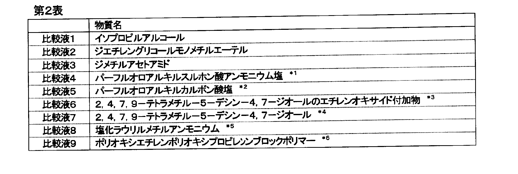
*2,「サーフロンS-111(商品名)」;AGCセイミケミカル(株)製,0.01%水
*3,「サーフィノール420(商品名)」;日信化学工業株式会社製,0.01%水
*4,「サーフィノール104(商品名)」;日信化学工業株式会社製,0.01%水
*5,「カチオーゲンTML(商品名)」;第一工業製薬株式会社製,0.01%水
*6,「エパン420(商品名)」;第一工業製薬株式会社製,0.01%水
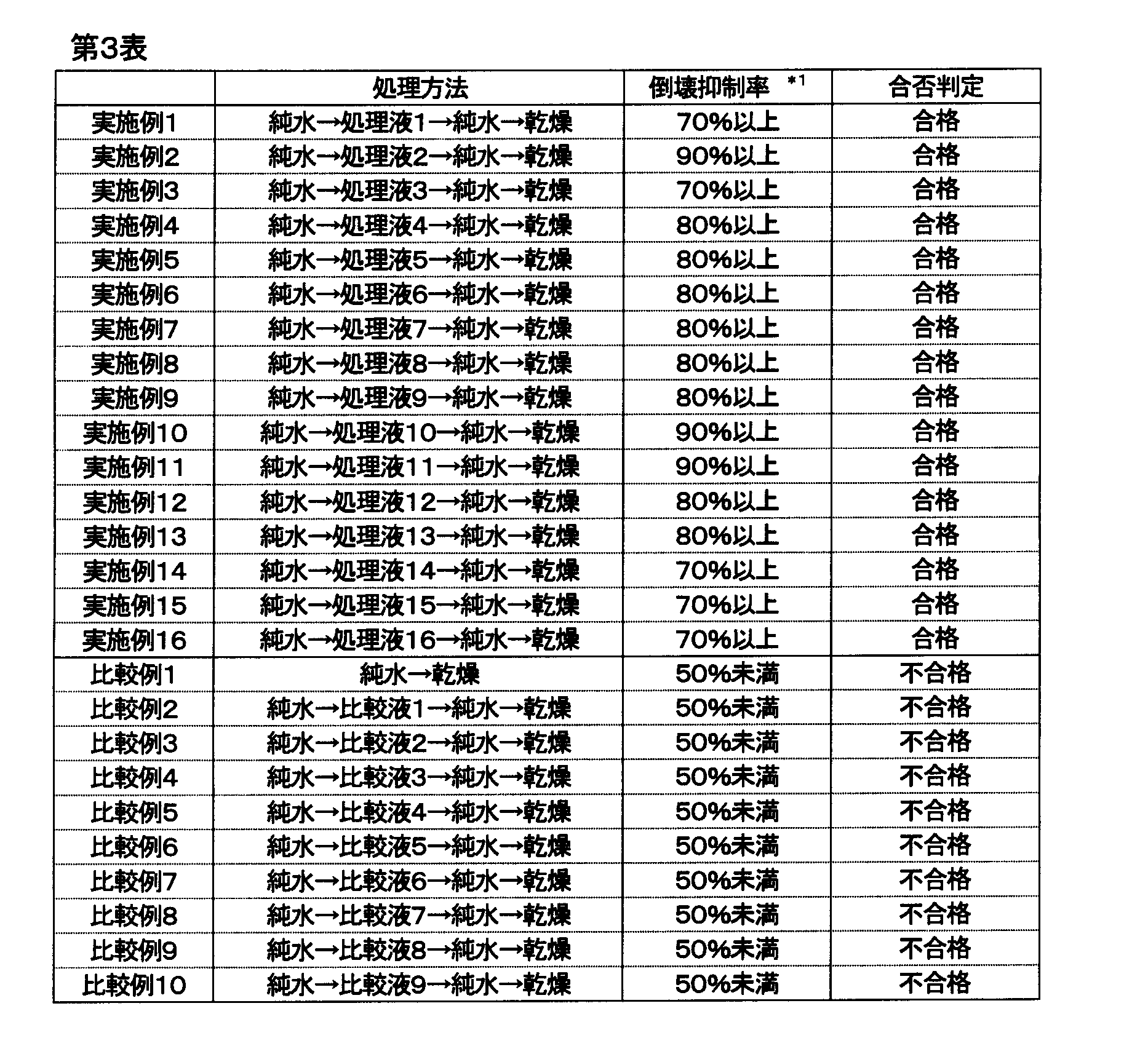
実施例1~16において、金属107として窒化チタンの代わりにタングステンを用いた以外は実施例1~16と同様にして、実施例17~32の図-1(g)に示す構造体を得た。得られた構造体は、金属(タングステン)の円筒108の円筒状のパターン(φ125nm,高さ:1200nm(アスペクト比:9.6),円筒と円筒との間の距離:50nm)を有する微細構造であり、70%以上の該パターンは倒壊することがなかった。各例において使用した処理液1~16の組成を第1表に、また各例で用いた処理液、処理方法及び倒壊抑制率の結果を第4表に示す。
比較例1~10において、金属107として窒化チタンの代わりにタングステンを用いた以外は比較例1~10と同様にして、各々比較例11~20の図-1(g)に示す構造体を得た。得られた構造体のパターンの50%以上は、図-1(h)に示されるような倒壊をおこしていた。各例において使用した比較液1~9の組成を第2表に、また各例で用いた比較液、処理方法及び倒壊抑制率の結果を第4表に示す。
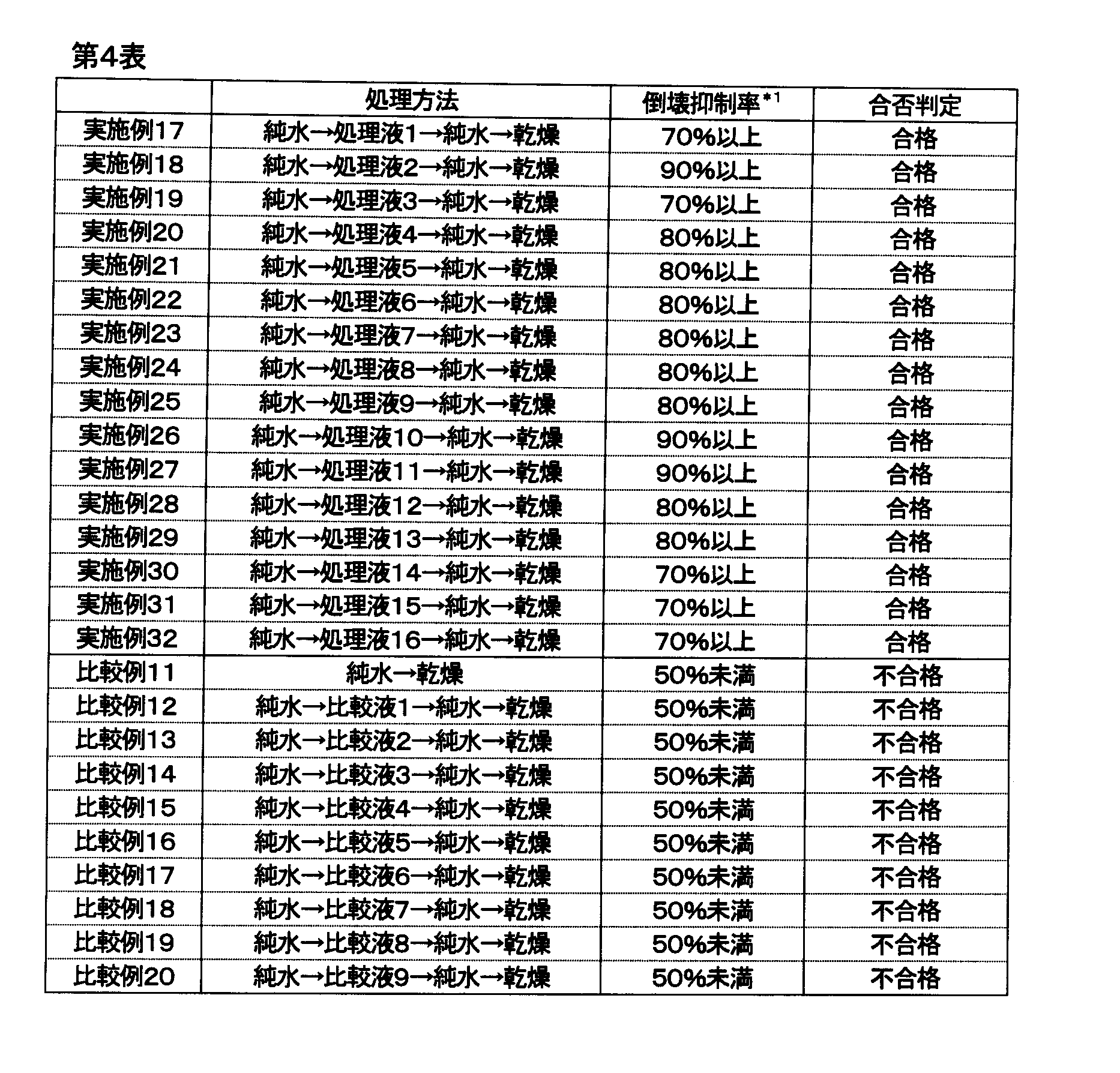
実施例1~16において、金属107として窒化チタンの代わりにタンタルを用いた以外は実施例1~16と同様にして、各々実施例33~48の図-1(g)に示す構造体を得た。得られた構造体は、金属(タンタル)の円筒108の円筒状のパターン(φ125nm,高さ:1200nm(アスペクト比:9.6),円筒と円筒との間の距離:50nm)を有する微細構造であり、70%以上の該パターンは倒壊することがなかった。各例において使用した処理液1~16の組成を第1表に、また各例で用いた処理液、処理方法及び倒壊抑制率の結果を第5表に示す。
比較例1~10において、金属107として窒化チタンの代わりにタンタルを用いた以外は比較例1~10と同様にして、各々比較例21~30の図-1(g)に示す構造体を得た。得られた構造体のパターンの50%以上は、図-1(h)に示されるような倒壊をおこしていた。各例において使用した比較液1~9の組成を第2表に、また各例で用いた比較液、処理方法及び倒壊抑制率の結果を第5表に示す。
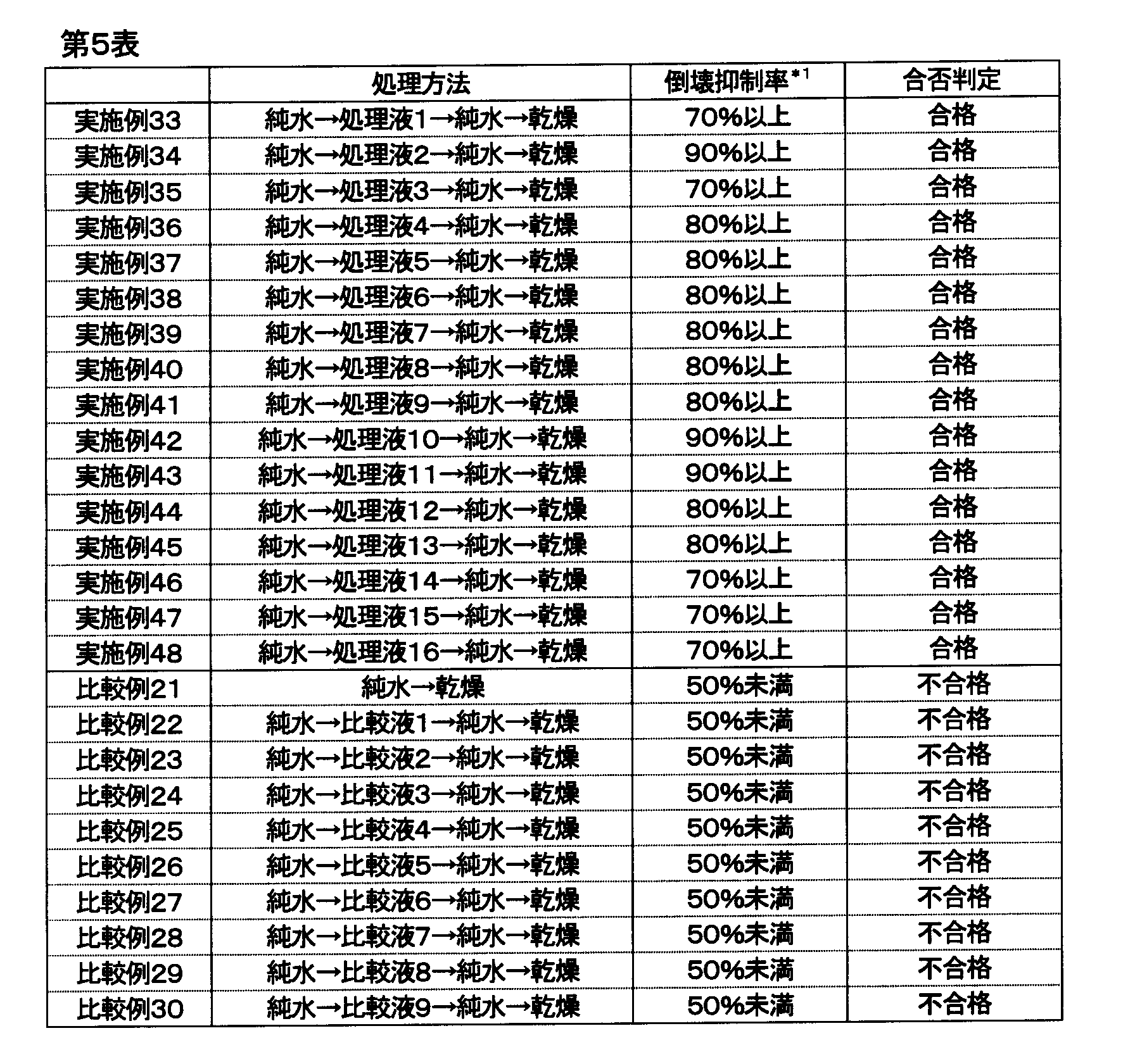
図-2(a)に示すように、シリコン基板上に形成された酸化珪素層201上にポリシリコン202(厚さ:100nm)を成膜し、その上にフォトレジスト203を形成した後、該フォトレジスト203を露光、現像することにより、図-2(b)に示す角柱状開口部204(1000nm×8000nm)を形成し、該フォトレジスト203をマスクとしてドライエッチングによりポリシリコン202に図-2(c)に示す角柱状の孔205を、酸化珪素層201までエッチングして形成した。次いで、フォトレジスト203をアッシングにより除去し、図-2(d)に示すポリシリコン202に酸化珪素層201に達する角柱状孔205が開孔された構造体を得た。得られた構造体の角柱状孔205に金属としてチタンを充填・堆積して、金属(チタン)角柱206及び金属(チタン)層207を形成し(図-2(e))、該金属(チタン)層207上にフォトレジスト208を形成した(図-2(f))。次いで、フォトレジスト208を露光、現像することにより、図-2(g)に示す2つの金属(チタン)角柱206を含む範囲を覆う長方形型フォトマスク209を形成し、該長方形型フォトマスク209をマスクとして、金属(チタン)層207をドライエッチングすることにより、図-2(h)に示す下部の両端に金属(チタン)角柱206を有する金属(チタン)板210を形成した。さらに、長方形フォトマスク209をアッシングにより除去し、図-2(i)に示すポリシリコン202と金属(チタン)角柱206とを有する金属(チタン)板210からなる構造体を得た。得られた構造体のポリシリコン202を水酸化テトラメチルアンミニウム水溶液により溶解除去した後、純水、処理液1~16、及び純水の順で接液処理し、乾燥を行い、実施例49~64の図-2(j)に示す橋梁構造体211を得た。
得られた橋梁構造体211は、金属(チタン)板210(縦×横:15000nm×10000nm,厚さ:300nm,アスペクト比:50)及びその両端に金属(チタン)角柱(縦×横:1000nm×8000nm,高さ:100nm)を有する微細構造であるが、70%以上の金属(チタン)板210が倒壊することがなく、酸化珪素層201に触れることはなかった。ここで、パターンの倒壊は、「FE-SEM S-5500(型番)」:日立ハイテクノロジーズ社製を用いて観察した。各例において使用した処理液1~16の組成を第1表に、また各例で用いた処理液、処理方法及び倒壊抑制率の結果を第6表に示す。
実施例49において、図-2(i)に示される構造体のポリシリコン202を水酸化テトラメチルアンミニウム水溶液により溶解除去した後、純水のみで処理した以外は、実施例49と同様にして図-2(j)に示す橋梁構造体211を得た。得られた橋梁構造体211の50%以上は、図-2(k)に示されるような倒壊をおこしていた。比較例31において使用した処理液、処理方法及び倒壊抑制率の結果を第6表に示す。
実施例49において、図-2(i)に示される構造体のポリシリコン202を水酸化テトラメチルアンミニウム水溶液により溶解除去し純水で処理した後、処理液1の代わりに第2表に示す比較液1~9で処理する以外は、実施例49と同様にして、比較例32~40の図-2(j)に示す橋梁構造体211を得た。得られた橋梁構造体211の50%以上は、図-2(k)に示されるような倒壊をおこしていた(倒壊抑制率は50%未満となった。)。比較例31において使用した比較液1~9の組成を第2表に、また各例で用いた比較液、処理方法及び倒壊抑制率を第6表に示す。

実施例49~64において、金属としてチタンの代わりに酸化アルミニウムを用いた以外は実施例49~64と同様にして、実施例65~80の図-2(j)に示す橋梁構造体211を得た。
得られた橋梁構造体211は、金属(酸化アルミニウム)板210(縦×横:15000nm×10000nm,厚さ:300nm,アスペクト比:50)及びその両端に金属(酸化アルミニウム)角柱(縦×横:1000nm×8000nm,高さ:100nm)を有する微細構造であるが、70%以上の金属(酸化アルミニウム)板210が倒壊することなく、酸化珪素層201に触れることはなかった。各例において使用した処理液1~16の組成を第1表に、また各例で用いた処理液、処理方法及び倒壊抑制率の結果を第7表に示す。
比較例31~40において、金属としてチタンの代わりに酸化アルミニウムを用いた以外は比較例31~40と同様にして、比較例41~50の図-2(j)に示す橋梁構造体211を得た。得られた橋梁構造体の50%以上は、図-2(k)に示されるような倒壊をおこしていた。各例において使用した比較液1~9の組成を第2表に、また各例で用いた比較液、処理方法及び倒壊抑制率の結果を第7表に示す。
実施例49~64において、金属としてチタンの代わりに酸化ハフニウムを用いた以外は実施例49~64と同様にして、実施例81~96の図-2(j)に示す橋梁構造体211を得た。
得られた橋梁構造体211は、金属(酸化ハフニウム)板210(縦×横:15000nm×10000nm,厚さ:300nm,アスペクト比:50)及びその両端に金属(酸化ハフニウム)角柱(縦×横:1000nm×8000nm,高さ:100nm)を有する微細構造であるが、70%以上の金属(酸化ハフニウム)板210が倒壊することがなく、酸化珪素層201に触れることはなかった。各例において使用した処理液1~16の組成を第1表に、また各例で用いた処理液、処理方法及び倒壊抑制率の結果を第8表に示す。
比較例31~40において、金属としてチタンの代わりに酸化ハフニウムを用いた以外は比較例31~40と同様にして、比較例51~60の図-2(j)に示す橋梁構造体211を得た。得られた橋梁構造体の50%以上は、図-2(k)に示されるような倒壊をおこしていた。各例において使用した比較液1~9の組成を第2表に、また各例で用いた比較液、処理方法及び倒壊抑制率の結果を第8表に示す。

実施例49~64において、金属としてチタンの代わりにルテニウムを用いた以外は実施例49~64と同様にして、実施例97~112の図-2(j)に示す橋梁構造体211を得た。
得られた橋梁構造体211は、金属(ルテニウム)板210(縦×横:15000nm×10000nm,厚さ:300nm,アスペクト比:50)及びその両端に金属(ルテニウム)角柱(縦×横:1000nm×8000nm,高さ:100nm)を有する微細構造であるが、70%以上の金属(ルテニウム)板210が倒壊することはなく、酸化珪素層201に触れることはなかった。ここで、パターンの倒壊は、「FE-SEM S-5500(型番)」:日立ハイテクノロジーズ社製を用いて観察した。各例において使用した処理液1~16の組成を第1表に、また各例で用いた処理液、処理方法及び倒壊抑制率の結果を第9表に示す。
比較例31~40において、金属としてチタンの代わりにルテニウムを用いた以外は比較例31~40と同様にして、比較例61~70の図-2(j)に示す橋梁構造体211を得た。得られた橋梁構造体の50%以上は、図-2(k)に示されるような倒壊をおこしていた。各例において使用した比較液1~9の組成を第2表に、また各例で用いた比較液、処理方法及び倒壊抑制率の結果を第9表に示す。

Claims (9)
- リン酸エステル及び/又はポリオキシアルキレンエーテルリン酸エステルを含む金属微細構造体のパターン倒壊抑制用処理液。
- リン酸エステル及び/又はポリオキシアルキレンエーテルリン酸エステルが、下記一般式(1)及び/又は一般式(2):

で表されるものである請求項1に記載の処理液。 - さらに水を含む請求項1又は2に記載の処理液。
- 前記一般式(1)及び(2)におけるOR2が、オキシエチレン基及び/又はオキシプロピレン基である請求項1~3のいずれかに記載の処理液。
- リン酸エステル及び/又はポリオキシアルキレンエーテルリン酸エステルの含有量が10ppm~50%である請求項1~4のいずれかに記載の処理液。
- 金属微細構造体のパターンが、窒化チタン、チタン、ルテニウム、酸化ルテニウム、タングステン、タングステンシリサイド、窒化タングステン、酸化アルミニウム、酸化ハフニウム、ハフニウムシリケート、窒化ハフニウムシリケート、白金、タンタル、酸化タンタル、窒化タンタル、ニッケルシリサイド、ニッケルシリコンゲルマニウム、ニッケルゲルマニウムから選ばれる少なくとも一種の材料を用いてなるものである請求項1~5のいずれかに記載の処理液。
- ウェットエッチング又はドライエッチングの後の洗浄工程において、請求項1~6のいずれかに記載の処理液を用いることを特徴とする金属微細構造体の製造方法。
- 金属微細構造体のパターンが、窒化チタン、チタン、ルテニウム、酸化ルテニウム、タングステン、タングステンシリサイド、窒化タングステン、酸化アルミニウム、酸化ハフニウム、ハフニウムシリケート、窒化ハフニウムシリケート、白金、タンタル、酸化タンタル、窒化タンタル、ニッケルシリサイド、ニッケルシリコンゲルマニウム、ニッケルゲルマニウムから選ばれる少なくとも一種の材料を用いてなるものである請求項7に記載の製造方法。
- 金属微細構造体が、半導体装置又はマイクロマシンである請求項7又は8に記載の製造方法。
Priority Applications (4)
| Application Number | Priority Date | Filing Date | Title |
|---|---|---|---|
| US13/388,462 US9196472B2 (en) | 2009-08-07 | 2010-07-21 | Processing liquid for suppressing pattern collapse of fine metal structure, and method for producing fine metal structure using same |
| KR1020127002090A KR101750573B1 (ko) | 2009-08-07 | 2010-07-21 | 금속 미세 구조체의 패턴 도괴 억제용 처리액 및 이것을 이용한 금속 미세 구조체의 제조 방법 |
| CN201080035064.5A CN102484056B (zh) | 2009-08-07 | 2010-07-21 | 用于抑制金属微细结构体的图案倒塌的处理液和使用其的金属微细结构体的制造方法 |
| DE112010003217.3T DE112010003217B4 (de) | 2009-08-07 | 2010-07-21 | Verarbeitungsflüssigkeit zur Unterdrückung eines Musterzusammenbruchs einer feinen Struktur, die aus einem Metall, einem Metallnitrid oder einem Metalloxid gebildet ist, und Verfahren zur Herstellung der feinen Struktur, bei dem diese eingesetzt wird |
Applications Claiming Priority (2)
| Application Number | Priority Date | Filing Date | Title |
|---|---|---|---|
| JP2009-185124 | 2009-08-07 | ||
| JP2009185124A JP5206622B2 (ja) | 2009-08-07 | 2009-08-07 | 金属微細構造体のパターン倒壊抑制用処理液及びこれを用いた金属微細構造体の製造方法 |
Publications (1)
| Publication Number | Publication Date |
|---|---|
| WO2011016337A1 true WO2011016337A1 (ja) | 2011-02-10 |
Family
ID=43544235
Family Applications (1)
| Application Number | Title | Priority Date | Filing Date |
|---|---|---|---|
| PCT/JP2010/062273 Ceased WO2011016337A1 (ja) | 2009-08-07 | 2010-07-21 | 金属微細構造体のパターン倒壊抑制用処理液及びこれを用いた金属微細構造体の製造方法 |
Country Status (7)
| Country | Link |
|---|---|
| US (1) | US9196472B2 (ja) |
| JP (1) | JP5206622B2 (ja) |
| KR (1) | KR101750573B1 (ja) |
| CN (1) | CN102484056B (ja) |
| DE (1) | DE112010003217B4 (ja) |
| TW (1) | TWI530588B (ja) |
| WO (1) | WO2011016337A1 (ja) |
Cited By (4)
| Publication number | Priority date | Publication date | Assignee | Title |
|---|---|---|---|---|
| CN103260841A (zh) * | 2011-05-26 | 2013-08-21 | 三菱丽阳株式会社 | 表面具有微细凹凸结构的物品的制造方法 |
| CN103430102A (zh) * | 2011-03-18 | 2013-12-04 | 巴斯夫欧洲公司 | 制造具有带50nm及更小行间距尺寸的图案化材料层的集成电路装置、光学装置、微型电机和机械精密装置的方法 |
| JP2015035458A (ja) * | 2013-08-08 | 2015-02-19 | 三菱瓦斯化学株式会社 | 微細構造体のパターン倒壊抑制用処理液及びこれを用いた微細構造体の製造方法 |
| JP2016507158A (ja) * | 2013-01-24 | 2016-03-07 | コーニング インコーポレイテッド | ポリマーナノマスクを使用した表面ナノ複製 |
Families Citing this family (9)
| Publication number | Priority date | Publication date | Assignee | Title |
|---|---|---|---|---|
| US8440573B2 (en) * | 2010-01-26 | 2013-05-14 | Lam Research Corporation | Method and apparatus for pattern collapse free wet processing of semiconductor devices |
| US8617993B2 (en) * | 2010-02-01 | 2013-12-31 | Lam Research Corporation | Method of reducing pattern collapse in high aspect ratio nanostructures |
| US8932933B2 (en) * | 2012-05-04 | 2015-01-13 | Micron Technology, Inc. | Methods of forming hydrophobic surfaces on semiconductor device structures, methods of forming semiconductor device structures, and semiconductor device structures |
| KR102167993B1 (ko) * | 2012-06-22 | 2020-10-21 | 아반토 퍼포먼스 머티리얼즈, 엘엘씨 | TiN 패턴 붕괴를 방지하기 위한 린싱 용액 |
| KR102899531B1 (ko) * | 2016-03-31 | 2025-12-12 | 후지필름 가부시키가이샤 | 반도체 제조용 처리액, 반도체 제조용 처리액이 수용된 수용 용기, 패턴 형성 방법 및 전자 디바이스의 제조 방법 |
| US11270909B2 (en) | 2020-01-27 | 2022-03-08 | Micron Technology, Inc. | Apparatus with species on or in conductive material on elongate lines |
| CN113889404B (zh) | 2020-07-02 | 2024-07-05 | 长鑫存储技术有限公司 | 半导体结构的处理方法及形成方法 |
| CN113889405B (zh) | 2020-07-02 | 2024-07-05 | 长鑫存储技术有限公司 | 半导体结构的处理方法及形成方法 |
| JP7801577B2 (ja) * | 2022-05-06 | 2026-01-19 | 日亜化学工業株式会社 | ステンレス板の製造方法及びステンレス板を用いた発光装置の製造方法 |
Citations (2)
| Publication number | Priority date | Publication date | Assignee | Title |
|---|---|---|---|---|
| JPH11249323A (ja) * | 1998-03-05 | 1999-09-17 | Kao Corp | レジスト現像方法 |
| JP2007213013A (ja) * | 2006-01-11 | 2007-08-23 | Tokyo Ohka Kogyo Co Ltd | リソグラフィー用洗浄剤及びそれを用いたレジストパターン形成方法 |
Family Cites Families (29)
| Publication number | Priority date | Publication date | Assignee | Title |
|---|---|---|---|---|
| US3723313A (en) * | 1971-03-24 | 1973-03-27 | Mobil Oil Corp | Lubricant useful in metal working |
| AU527434B2 (en) * | 1980-09-19 | 1983-03-03 | Soc Nat Elf Aquit (Prod) | Microemulsion of nutrients for microorganisms |
| US4451709A (en) * | 1981-12-21 | 1984-05-29 | Beltone Electronics Corporation | Eye glass hearing aids |
| US5232742A (en) * | 1992-05-15 | 1993-08-03 | Bridgestone/Firestone, Inc. | Spin finish composition |
| US5401590A (en) * | 1992-12-07 | 1995-03-28 | Duracell Inc. | Additives for electrochemical cells having zinc anodes |
| US5851108A (en) * | 1995-01-17 | 1998-12-22 | Beaudreau Electronics, Inc. | Electronic control sensor systems |
| JP4180716B2 (ja) | 1998-12-28 | 2008-11-12 | 富士通株式会社 | 半導体装置の製造方法 |
| JP2001342394A (ja) * | 2000-06-01 | 2001-12-14 | Mitsubishi Pencil Co Ltd | 筆記具用水性インキ組成物 |
| KR100398141B1 (ko) * | 2000-10-12 | 2003-09-13 | 아남반도체 주식회사 | 화학적 기계적 연마 슬러리 조성물 및 이를 이용한반도체소자의 제조방법 |
| US6451510B1 (en) * | 2001-02-21 | 2002-09-17 | International Business Machines Corporation | Developer/rinse formulation to prevent image collapse in resist |
| JP4724959B2 (ja) * | 2001-07-02 | 2011-07-13 | 三菱瓦斯化学株式会社 | フォトレジスト剥離剤組成物 |
| JP2003122027A (ja) | 2001-10-16 | 2003-04-25 | Sumitomo Chem Co Ltd | 剥離剤組成物 |
| JP2003177556A (ja) * | 2001-12-12 | 2003-06-27 | Sharp Corp | フォトレジスト剥離剤組成物および剥離方法 |
| JP2003195518A (ja) * | 2001-12-14 | 2003-07-09 | Shipley Co Llc | フォトレジスト用現像液 |
| TWI339680B (en) | 2002-02-19 | 2011-04-01 | Kanto Kagaku | Washing liquid composition for semiconductor substrate |
| JP4045180B2 (ja) | 2002-12-03 | 2008-02-13 | Azエレクトロニックマテリアルズ株式会社 | リソグラフィー用リンス液およびそれを用いたレジストパターン形成方法 |
| US7147700B2 (en) * | 2002-12-27 | 2006-12-12 | Brother Kogyo Kabushiki Kaisha | Water base ink for ink-jet recording |
| SG129274A1 (en) * | 2003-02-19 | 2007-02-26 | Mitsubishi Gas Chemical Co | Cleaaning solution and cleaning process using the solution |
| JP4470144B2 (ja) | 2003-03-19 | 2010-06-02 | エルピーダメモリ株式会社 | 半導体集積回路装置の製造方法 |
| JP4493393B2 (ja) | 2004-04-23 | 2010-06-30 | 東京応化工業株式会社 | リソグラフィー用リンス液 |
| JP4428642B2 (ja) | 2004-04-30 | 2010-03-10 | 東京応化工業株式会社 | パターン微細化用被覆形成剤およびそれを用いた微細パターンの形成方法 |
| EP1628336B1 (en) * | 2004-08-18 | 2012-01-04 | Mitsubishi Gas Chemical Company, Inc. | Cleaning liquid and cleaning method |
| JP4353090B2 (ja) | 2004-12-10 | 2009-10-28 | 三菱電機株式会社 | レジスト用現像液 |
| US7741257B2 (en) * | 2005-03-15 | 2010-06-22 | Ecolab Inc. | Dry lubricant for conveying containers |
| KR101330509B1 (ko) * | 2005-12-01 | 2013-11-15 | 미츠비시 가스 가가쿠 가부시키가이샤 | 반도체 소자 또는 표시 소자용 세정액 및 세정 방법 |
| TW200732863A (en) | 2006-01-11 | 2007-09-01 | Tokyo Ohka Kogyo Co Ltd | Detergent for lithography and method of forming resist pattern with the same |
| JP2007335892A (ja) | 2007-08-17 | 2007-12-27 | Toshiba Corp | 半導体装置 |
| JP5223273B2 (ja) * | 2007-09-05 | 2013-06-26 | 住友化学株式会社 | 水性懸濁状農薬組成物 |
| JP4655083B2 (ja) | 2007-11-16 | 2011-03-23 | セイコーエプソン株式会社 | 微小電気機械装置 |
-
2009
- 2009-08-07 JP JP2009185124A patent/JP5206622B2/ja active Active
-
2010
- 2010-07-21 WO PCT/JP2010/062273 patent/WO2011016337A1/ja not_active Ceased
- 2010-07-21 DE DE112010003217.3T patent/DE112010003217B4/de active Active
- 2010-07-21 KR KR1020127002090A patent/KR101750573B1/ko active Active
- 2010-07-21 CN CN201080035064.5A patent/CN102484056B/zh active Active
- 2010-07-21 US US13/388,462 patent/US9196472B2/en active Active
- 2010-08-04 TW TW099125930A patent/TWI530588B/zh active
Patent Citations (2)
| Publication number | Priority date | Publication date | Assignee | Title |
|---|---|---|---|---|
| JPH11249323A (ja) * | 1998-03-05 | 1999-09-17 | Kao Corp | レジスト現像方法 |
| JP2007213013A (ja) * | 2006-01-11 | 2007-08-23 | Tokyo Ohka Kogyo Co Ltd | リソグラフィー用洗浄剤及びそれを用いたレジストパターン形成方法 |
Cited By (7)
| Publication number | Priority date | Publication date | Assignee | Title |
|---|---|---|---|---|
| CN103430102A (zh) * | 2011-03-18 | 2013-12-04 | 巴斯夫欧洲公司 | 制造具有带50nm及更小行间距尺寸的图案化材料层的集成电路装置、光学装置、微型电机和机械精密装置的方法 |
| EP2686737A4 (en) * | 2011-03-18 | 2014-09-03 | Basf Se | METHOD FOR PRODUCING INTEGRATED SWITCHING DEVICES, OPTICAL DEVICES, MICROMATIC MACHINES AND MECHANICAL PRECISION DEVICES WITH STRUCTURED MATERIAL LAYERS WITH LINE DISTANCE DISTANCE OF 50 NM OR LESS |
| US9184057B2 (en) | 2011-03-18 | 2015-11-10 | Basf Se | Method for manufacturing integrated circuit devices, optical devices, micromachines and mechanical precision devices having patterned material layers with line-space dimensions of 50 nm and less |
| CN103260841A (zh) * | 2011-05-26 | 2013-08-21 | 三菱丽阳株式会社 | 表面具有微细凹凸结构的物品的制造方法 |
| US9138775B2 (en) | 2011-05-26 | 2015-09-22 | Mitsubishi Rayon Co., Ltd. | Method for preparing article having uneven microstructure on surface thereof |
| JP2016507158A (ja) * | 2013-01-24 | 2016-03-07 | コーニング インコーポレイテッド | ポリマーナノマスクを使用した表面ナノ複製 |
| JP2015035458A (ja) * | 2013-08-08 | 2015-02-19 | 三菱瓦斯化学株式会社 | 微細構造体のパターン倒壊抑制用処理液及びこれを用いた微細構造体の製造方法 |
Also Published As
| Publication number | Publication date |
|---|---|
| KR20120062683A (ko) | 2012-06-14 |
| TWI530588B (zh) | 2016-04-21 |
| JP5206622B2 (ja) | 2013-06-12 |
| US20120135604A1 (en) | 2012-05-31 |
| US9196472B2 (en) | 2015-11-24 |
| CN102484056A (zh) | 2012-05-30 |
| DE112010003217B4 (de) | 2021-02-04 |
| KR101750573B1 (ko) | 2017-06-23 |
| JP2011040502A (ja) | 2011-02-24 |
| CN102484056B (zh) | 2015-09-30 |
| TW201113394A (en) | 2011-04-16 |
| DE112010003217T5 (de) | 2012-07-12 |
Similar Documents
| Publication | Publication Date | Title |
|---|---|---|
| JP5206622B2 (ja) | 金属微細構造体のパターン倒壊抑制用処理液及びこれを用いた金属微細構造体の製造方法 | |
| JP5664653B2 (ja) | 微細構造体のパターン倒壊抑制用処理液及びこれを用いた微細構造体の製造方法 | |
| CN102598220B (zh) | 用于抑制金属微细结构体的图案倒塌的处理液和使用其的金属微细结构体的制造方法 | |
| JP5720575B2 (ja) | 金属微細構造体のパターン倒壊抑制用処理液及びこれを用いた金属微細構造体の製造方法 | |
| JP5720572B2 (ja) | 金属微細構造体のパターン倒壊抑制用処理液及びこれを用いた金属微細構造体の製造方法 | |
| JP5741589B2 (ja) | 微細構造体のパターン倒壊抑制用処理液及びこれを用いた微細構造体の製造方法 | |
| JP5741590B2 (ja) | 微細構造体のパターン倒壊抑制用処理液及びこれを用いた微細構造体の製造方法 | |
| JP6119285B2 (ja) | 微細構造体のパターン倒壊抑制用処理液及びこれを用いた微細構造体の製造方法 | |
| JP6405610B2 (ja) | 高アスペクト比を有する微細構造体のパターン倒壊抑制用処理液およびこれを用いた微細構造体の製造方法 | |
| JP2015035458A (ja) | 微細構造体のパターン倒壊抑制用処理液及びこれを用いた微細構造体の製造方法 |
Legal Events
| Date | Code | Title | Description |
|---|---|---|---|
| WWE | Wipo information: entry into national phase |
Ref document number: 201080035064.5 Country of ref document: CN |
|
| 121 | Ep: the epo has been informed by wipo that ep was designated in this application |
Ref document number: 10806337 Country of ref document: EP Kind code of ref document: A1 |
|
| ENP | Entry into the national phase |
Ref document number: 20127002090 Country of ref document: KR Kind code of ref document: A |
|
| WWE | Wipo information: entry into national phase |
Ref document number: 13388462 Country of ref document: US |
|
| WWE | Wipo information: entry into national phase |
Ref document number: 112010003217 Country of ref document: DE Ref document number: 1120100032173 Country of ref document: DE |
|
| 122 | Ep: pct application non-entry in european phase |
Ref document number: 10806337 Country of ref document: EP Kind code of ref document: A1 |