WO2011010423A1 - 両面研磨装置用キャリアの製造方法、両面研磨装置用キャリア及びウェーハの両面研磨方法 - Google Patents
両面研磨装置用キャリアの製造方法、両面研磨装置用キャリア及びウェーハの両面研磨方法 Download PDFInfo
- Publication number
- WO2011010423A1 WO2011010423A1 PCT/JP2010/004077 JP2010004077W WO2011010423A1 WO 2011010423 A1 WO2011010423 A1 WO 2011010423A1 JP 2010004077 W JP2010004077 W JP 2010004077W WO 2011010423 A1 WO2011010423 A1 WO 2011010423A1
- Authority
- WO
- WIPO (PCT)
- Prior art keywords
- wafer
- carrier
- double
- resin insert
- inner peripheral
- Prior art date
Links
Images


Classifications
-
- B—PERFORMING OPERATIONS; TRANSPORTING
- B24—GRINDING; POLISHING
- B24B—MACHINES, DEVICES, OR PROCESSES FOR GRINDING OR POLISHING; DRESSING OR CONDITIONING OF ABRADING SURFACES; FEEDING OF GRINDING, POLISHING, OR LAPPING AGENTS
- B24B37/00—Lapping machines or devices; Accessories
- B24B37/27—Work carriers
- B24B37/28—Work carriers for double side lapping of plane surfaces
-
- Y—GENERAL TAGGING OF NEW TECHNOLOGICAL DEVELOPMENTS; GENERAL TAGGING OF CROSS-SECTIONAL TECHNOLOGIES SPANNING OVER SEVERAL SECTIONS OF THE IPC; TECHNICAL SUBJECTS COVERED BY FORMER USPC CROSS-REFERENCE ART COLLECTIONS [XRACs] AND DIGESTS
- Y10—TECHNICAL SUBJECTS COVERED BY FORMER USPC
- Y10T—TECHNICAL SUBJECTS COVERED BY FORMER US CLASSIFICATION
- Y10T29/00—Metal working
- Y10T29/49—Method of mechanical manufacture
- Y10T29/49826—Assembling or joining
Definitions
- the present invention relates to a carrier for a double-side polishing apparatus used when simultaneously polishing both surfaces of a wafer, a manufacturing method thereof, and a double-side polishing method of a wafer using a double-side polishing apparatus.
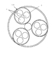
- FIG. 8 is a schematic explanatory view for explaining polishing of a wafer by a general double-side polishing apparatus conventionally used.
- the carrier 101 for a double-side polishing apparatus is formed to be thinner than the wafer W, and holds the wafer W at a predetermined position between the upper surface plate 108 and the lower surface plate 109 of the double-side polishing device 120.
- a holding hole 104 is provided.
- the wafer W is inserted and held in the holding hole 104, and the upper and lower surfaces of the wafer W are sandwiched between the polishing cloths 110 provided on the opposing surfaces of the upper surface plate 108 and the lower surface plate 109.
- the double-side polishing machine carrier 101 is engaged with the sun gear 111 and the internal gear 112 and is rotated and revolved by the driving rotation of the sun gear 111. Then, the upper surface plate 108 and the lower surface plate 109 are rotated in reverse while supplying the abrasive to the polishing surface, whereby both surfaces of the wafer W are simultaneously polished with the polishing cloth 110 attached to the upper and lower surface plates.
- the carrier 101 for the double-side polishing apparatus used in such a double-side polishing process for the wafer W is mainly made of metal.
- the resin insert 103 is attached along the inner peripheral portion of the holding hole 104 formed in the carrier main body 102.
- the outer periphery of the resin insert is wedge-shaped and fitted into the carrier body, and further fixed with an adhesive, in order to prevent the resin insert from being detached during processing or conveyance. (See Patent Document 1).
- the present inventor investigated the cause of the occurrence of such a wafer sagging and nanotopology failure.
- FIGS. 9A and 9B the resin insert 103 in contact with the peripheral portion of the wafer W to be polished is shown.
- the force by which the carrier 101 presses the wafer W includes not only a component parallel to the polishing cloth or the main surface 105 of the carrier but also a component pressing upward or downward.
- the wafer W is locally pressed against the polishing cloth, and the outer peripheral sagging or nanotopology failure occurs.
- the carrier body and the resin insert are first manufactured separately, and then the resin insert is mounted on the carrier body.
- the shape of the ring whose outer peripheral portion has a wedge shape is cut out from the resin base material, but since the width of the ring including the wedge is usually as small as 5 mm or less, the mechanical strength of this part is small, Easily distorted.
- the cut-out length of the wedge is larger than the length of the inner peripheral surface of the resin insert. Since this long processing length is accompanied by expansion of the resin base material due to generated processing heat, it is easily distorted before being inserted into the carrier body.
- the wedge-shaped fitting part of the carrier body and resin insert prevents the resin insert from falling off during use, so there is not much dimensional tolerance.
- the resin insert is deformed due to differences in processing accuracy and mechanical strength between the two. However, it is inserted into the carrier body. Thus, if the distorted resin insert is inserted into the carrier body having a small tolerance, the resin insert is further distorted as a result. For example, even if it is desired to make the inner peripheral surface of the resin insert perpendicular to the main surface of the carrier, the resin insert will not be perpendicular due to this distortion.
- the present invention has been made in view of the above-described problems, and is capable of accurately processing into a desired inner peripheral surface shape by suppressing distortion of the resin insert, and double-side polishing that can suppress outer peripheral sagging and nanotopology defects of a polished wafer. It aims at providing the manufacturing method of the carrier for apparatuses. Another object of the present invention is to provide a double-side polishing method for a wafer that can suppress peripheral sagging of the polished wafer and nanotopology failure due to distortion of the resin insert.
- a double-side polishing apparatus for polishing both surfaces of a wafer, it is disposed between upper and lower surface plates to which a polishing cloth is attached.
- a carrier main body formed with a holding hole for holding the wafer sandwiched therebetween, and an inner peripheral surface arranged along the inner periphery of the holding hole of the carrier main body and in contact with the peripheral edge of the held wafer.
- a carrier manufacturing method for a double-side polishing apparatus comprising: a ring-shaped resin insert having at least a base material of the resin insert in which an inner peripheral surface contacting the held wafer is not formed; After mounting in the hole, an inner peripheral surface forming process is performed on the base material of the resin insert to form an inner peripheral surface in contact with the peripheral portion of the held wafer. Method of manufacturing rear is provided.
- the inner peripheral surface is formed on the base material of the resin insert.
- the inner peripheral surface forming process can be performed such that an angle ⁇ between the inner peripheral surface of the resin insert and the main surface of the carrier body is 88 ° ⁇ ⁇ ⁇ 92 °.
- the inner peripheral surface forming process is performed such that the angle ⁇ between the inner peripheral surface of the resin insert and the main surface of the carrier body is 88 ° ⁇ ⁇ ⁇ 92 °, the outer periphery of the polishing wafer A carrier for a double-side polishing apparatus that can more reliably suppress sagging and nanotopology defects.
- a disk-shaped material or a ring-shaped material having an inner diameter smaller than the diameter of the wafer can be used as the base material of the resin insert.
- a disk-shaped thing is used as a base material of the said resin insert, it can suppress more reliably that a resin insert will be distorted.
- the ring-shaped thing which has an internal diameter smaller than the diameter of the said wafer is used as a base material of the said resin insert, distortion of the resin insert can fully be suppressed.
- the material of the base material of the resin insert can be an aramid resin.
- the mechanical strength of the wafer W can be increased while sufficiently exhibiting the effect of protecting the peripheral portion of the wafer W from damage by the carrier.
- the carrier for double-side polish apparatuses manufactured by the manufacturing method of the carrier for double-side polish apparatuses of this invention mentioned above is provided.
- the distortion of the resin insert is suppressed and the inner peripheral surface is accurately processed into a desired shape. Therefore, it becomes a carrier for a double-side polishing apparatus that can suppress peripheral sagging and nanotopology failure during wafer polishing.
- a ring-shaped resin insert having a holding hole for holding a wafer and an inner peripheral surface arranged along the inner periphery of the holding hole and in contact with the peripheral edge of the held wafer.
- a wafer double-side polishing method in which the wafer held by a carrier for a double-side polishing apparatus is sandwiched between upper and lower surface plates to which a polishing cloth is attached, and both surfaces of the wafer are simultaneously polished, and the wafer is polished Before, the angle ⁇ between the inner peripheral surface of the resin insert and the main surface of the carrier is inspected in advance, and the wafer is polished using only the inspected angle ⁇ satisfying 88 ° ⁇ ⁇ ⁇ 92 °.
- a double-side polishing method for a wafer is provided.
- the angle ⁇ between the inner peripheral surface of the resin insert and the main surface of the carrier is inspected in advance, and the inspected angle ⁇ satisfies 88 ° ⁇ ⁇ ⁇ 92 °. If the wafer is polished using only a wafer, it is possible to reliably suppress the peripheral sag and the nanotopology failure during the polishing of the wafer.
- a base material of a resin insert that is not formed with an inner peripheral surface in contact with a wafer to be held is mounted in a holding hole of a carrier body, Since the inner peripheral surface is formed on the base material to form the inner peripheral surface in contact with the peripheral edge of the held wafer, it is possible to accurately process the desired inner peripheral surface shape by suppressing distortion of the resin insert.
- a carrier for a double-side polishing apparatus that can suppress the sagging of the wafer to be polished and the nanotopology failure.
- the angle ⁇ between the inner peripheral surface of the resin insert and the main surface of the carrier is inspected in advance, and the inspected angle ⁇ is 88 ° ⁇ ⁇ ⁇ 92 °. Since the wafer is polished using only the one that satisfies the conditions, it is possible to reliably suppress the peripheral sag and the nanotopology failure during the polishing of the wafer.
- the present invention is not limited to this.
- the carrier body and the resin insert are separately produced, that is, after forming the inner peripheral surface of the resin insert into a ring shape, The resin insert was mounted on the carrier body.
- the resin insert is distorted.
- the inner peripheral surface of the resin insert is processed in advance so as to be perpendicular to the main surface of the carrier. Even in such a case, it has been found that the inner peripheral surface is inclined at a right angle due to distortion of the resin insert after mounting.
- the inner peripheral surface of the resin insert is formed after the base material of the resin insert is mounted on the carrier body, instead of forming the inner peripheral surface of the resin insert in advance. If the inner peripheral surface in contact with the peripheral edge of the wafer to be held is formed, distortion of the resin insert can be suppressed, and the inner peripheral surface of the resin insert is, for example, perpendicular to the main surface of the carrier. It was conceived that the desired shape can be formed with high accuracy.
- the angle ⁇ between the inner peripheral surface of the resin insert and the main surface of the carrier is inspected, and polishing is performed using only the angle ⁇ satisfying 88 ° ⁇ ⁇ ⁇ 92 °.
- FIG. 1 is a schematic view showing an example of a carrier for a double-side polishing apparatus of the present invention manufactured by the method for manufacturing a carrier for double-side polishing apparatus of the present invention
- FIG. 2 is a double-side polishing having this carrier for a double-side polishing apparatus. It is the schematic which showed an example of the apparatus.
- the double-side polishing apparatus carrier 1 has a carrier body 2 in which a holding hole 4 for holding a wafer W is formed.
- a resin insert 3 is arranged along the inner periphery of the holding hole 4 of the carrier body 2. The resin insert 3 can prevent damage to the peripheral edge of the wafer W due to the wafer W coming into contact with the carrier body 2 during polishing.
- the wafer W is inserted into the holding hole 4 of the carrier 1 for double-side polishing apparatus, and the inner peripheral surface 6 of the resin insert 3 and the peripheral edge of the wafer W are held in contact with each other.
- the carrier 1 for a double-side polishing apparatus is provided with a polishing liquid hole 13 for passing a polishing liquid separately from the holding hole 4, and an outer peripheral tooth 7 is provided on the outer peripheral portion.
- the double-side polishing apparatus 20 includes an upper surface plate 8 and a lower surface plate 9 provided opposite to each other in the vertical direction.
- a polishing cloth 10 is affixed.
- the wafer W is held in the holding hole 4 of the carrier 1 for double-side polishing apparatus and is sandwiched between the upper surface plate 8 and the lower surface plate 9.
- a sun gear 11 is provided at the center between the upper surface plate 8 and the lower surface plate 9, and an internal gear 12 is provided at the peripheral portion.
- the teeth of the sun gear 11 and the internal gear 12 are engaged with the outer peripheral teeth 7 of the carrier 1 for a double-side polishing apparatus, and the upper surface plate 8 and the lower surface plate 9 are rotated by a drive source (not shown). Accordingly, the carrier 1 for a double-side polishing apparatus revolves around the sun gear 11 while rotating.
- a carrier body of a carrier for a double-side polishing apparatus is produced.
- a holding hole 4 for holding the wafer W is formed in the carrier body 2.
- outer peripheral teeth 7 that mesh with the sun gear and the internal gear of the double-side polishing apparatus as described above are formed on the outer peripheral portion.
- a polishing liquid hole 13 for allowing the polishing liquid to pass through the carrier body 2 can be provided.
- the arrangement and the number of the polishing liquid holes 13 are not limited to those shown in FIG.
- the double-side polishing apparatus carrier 1 shown in FIG. 1 In the example of the double-side polishing apparatus carrier 1 shown in FIG. 1, one holding hole 4 is provided. However, as shown in FIG. 3, a plurality of holding holes 4 are provided in the double-side polishing apparatus carrier 31.
- the resin insert 3 may be disposed along the inner periphery of each holding hole 4.
- the material of the carrier body 2 is not particularly limited, but may be titanium, for example.
- the surface of the carrier body 2 can be coated with a DLC (Diamond Like Carbon) film having high hardness. By coating with the DLC film in this way, the durability of the carrier 1 for a double-side polishing apparatus can be improved, the carrier life can be extended, and the replacement frequency can be reduced.
- DLC Diamond Like Carbon
- a base material of the resin insert 3 in which the inner peripheral surface 6 that contacts the wafer W to be held is not formed is prepared.
- the outer periphery of the base material is formed and processed into a shape along the inner periphery of the holding hole 4 of the carrier body 2 produced as described above. And this base material is mounted
- the resin insert 3 can be made difficult to come off from the carrier body 2. . Furthermore, both can be fixed with an adhesive.
- the material of the base material of the resin insert 3 can be, for example, an aramid resin.
- the aramid resin is a material having a high strength and a high elastic modulus, and can improve the durability and protect the peripheral portion of the wafer W from damage caused by a carrier 1 for a double-side polishing apparatus made of metal such as titanium.
- an inner peripheral surface forming process is performed on the base material of the resin insert 3 in a state of being mounted in the holding hole 4 of the carrier main body 2 to form an inner peripheral surface in contact with the peripheral portion of the held wafer.
- the inner peripheral surface forming process of the base material of the resin insert 3 can be performed at low cost by mechanical grinding. Further, it is possible to perform processing at higher speed and with higher accuracy by using laser cutting.
- the base material of the resin insert 3 on which the inner peripheral surface is not formed is mounted on the carrier body 2 and the inner peripheral surface forming process of the resin insert 3 is performed, for example, the outer peripheral portion of the resin insert 3 is wedged.
- the wafer is polished using the carrier for a double-side polishing apparatus according to the present invention having a resin insert in which the inner peripheral surface shape is processed with high accuracy, the distortion of the wafer W and the nanotopology failure are reduced. Can be suppressed.
- the angle ⁇ between the inner peripheral surface 6 of the resin insert 3 and the main surface 5 of the carrier body 2 is 88 ° ⁇ ⁇ ⁇ 92.
- a disk-shaped material can be used as the base material of the resin insert 3.
- a base material 17 it is ensured that the base material 17 of the resin insert 3 is distorted when a wedge shape is formed on the outer peripheral portion of the base material 17 of the resin insert 3 and when it is attached to the carrier body 2. Therefore, the desired shape of the inner peripheral surface 6 can be accurately processed.
- a ring-shaped member having an inner diameter smaller than the diameter of the wafer W can be used as the base material 17 of the resin insert 3.
- the distortion of the resin insert 3 can be sufficiently suppressed to accurately process the shape of the desired inner peripheral surface 6, and the time required for the inner peripheral surface forming process can be reduced. In addition, it is possible to reduce the manufacturing process time of the carrier for the double-side polishing apparatus.
- the wafer double-side polishing method of the present invention will be described.
- a case where a double-side polishing apparatus as shown in FIG. 2 is used will be described.
- the angle ⁇ between the inner peripheral surface 6 of the resin insert 3 and the main surface 5 of the double-side polishing apparatus carrier 1 is inspected in advance. This inspection can be performed using, for example, a contour shape measuring machine.
- the carrier 1 for double-side polishing apparatus in which the angle ⁇ inspected in this way satisfies 88 ° ⁇ ⁇ ⁇ 92 ° is selected.
- the wafer W to be polished is held in the selected holding hole 4 of the carrier 1 for double-side polishing apparatus, the upper and lower polishing surfaces of the wafer W are sandwiched between the polishing cloths 10 affixed to the upper and lower surface plates 8 and 9, and the polishing agent is put on the polishing surface. Polishing while supplying. Further, other polishing conditions and the like can be performed in the same manner as in the conventional double-side polishing method. By polishing the wafer in this way, it is possible to reliably suppress the peripheral sagging and nanotopology failure of the wafer to be polished.
- the carrier in which the angle ⁇ between the inner peripheral surface 6 of the resin insert 3 and the main surface 5 of the carrier 1 for double-side polishing apparatus satisfies 88 ° ⁇ ⁇ ⁇ 92 ° depends on the method for manufacturing a carrier for double-side polishing apparatus of the present invention. It can be manufactured reliably.
- Example 1 A carrier for a double-side polishing apparatus as shown in FIG. 1 was manufactured using the method for manufacturing a carrier for a double-side polishing apparatus of the present invention.
- a titanium carrier body having one holding hole as shown in FIG. 1 is manufactured, and a base material of a disk-shaped resin insert as shown in FIG. 4 (A) is attached to the holding hole of the carrier body.
- the inner peripheral surface of the resin insert was formed by mechanical grinding. At this time, the inner peripheral surface was formed such that the angle ⁇ between the inner peripheral surface of the resin insert and the main surface of the carrier body was 90 °.
- an aramid resin was used as the material of the resin insert.
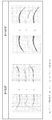
- double-side polishing of the silicon wafer is performed according to the double-side polishing method of the present invention, and the flatness and nanotopology of the wafer are evaluated. did. GBIR, SFQR, and Roll Off were measured as the flatness of the wafer.
- the method for manufacturing a carrier for a double-side polishing apparatus according to the present invention can be processed into a desired inner peripheral surface shape by suppressing distortion of the resin insert, and can suppress the outer peripheral sagging and nanotopology failure of the polished wafer. It was confirmed that a carrier for a double-side polishing apparatus could be manufactured. Moreover, it has confirmed that the double-sided polishing method of this invention can suppress the outer periphery sagging and nanotopology defect of a polishing wafer reliably.
- Example 2 A carrier for a double-side polishing apparatus was manufactured in the same manner as in Example 1 except that the angle ⁇ between the inner peripheral surface of the resin insert and the main surface of the carrier was 88 ° and 92 °. And evaluated in the same manner.
- the polished wafer flatness and nanotopology results are shown in FIG. As shown in FIG. 6, although the flatness and nanotopology are somewhat worse than the results of Example 1, the flatness and nanotopology are improved compared to the results of Comparative Examples described later, and good It turns out that it has become a result. Therefore, if the angle ⁇ is 88 ° ⁇ ⁇ ⁇ 92 °, it can be said that the peripheral sagging of the polished wafer and the nanotopology failure can be more reliably suppressed.
- a carrier body and a resin insert were separately manufactured, and then a carrier for a double-side polishing apparatus was manufactured by a conventional manufacturing method in which the resin insert was mounted on the carrier body.
- the resin insert was produced by processing its inner peripheral surface so as to have an angle of 90 ° with respect to the main surface of the carrier body. After mounting on the carrier, the resin insert was used using a contour shape measuring machine (Mitutoyo). When the angle ⁇ between the inner peripheral surface of the carrier and the main surface of the carrier was inspected, it was not 90 ° but was inclined. This may be due to distortion of the resin insert.
- the angle ⁇ between the inner peripheral surface of the resin insert of the carrier for the double-side polishing apparatus thus manufactured and the main surface of the carrier is inspected, and those having ⁇ of 72.5 ° and 107.5 ° are selected and silicon is selected.
- the wafer was subjected to double-side grinding, and the same evaluation as in Example 1 was performed. The result is shown in FIG. As shown in FIG. 6, it can be seen that the flatness and the nanotopology are deteriorated as compared with the results of Examples 1 and 2. Further, the brightness and darkness of the nanotopology is inverted according to the inclination inversion of the angle ⁇ . In other words, it can be seen that the surfaces of the wafer that sag are switched.
- FIG. 7 The result of measuring the shape of the front and back surfaces of the wafer at this time is shown in FIG. As shown in FIG. 7, it can be seen that the shape of the front and back surfaces of the wafer changes according to the angle ⁇ .
- the present invention is not limited to the above embodiment.
- the above-described embodiment is an exemplification, and the present invention has any configuration that has substantially the same configuration as the technical idea described in the claims of the present invention and that exhibits the same effects. Are included in the technical scope.
Landscapes
- Engineering & Computer Science (AREA)
- Mechanical Engineering (AREA)
- Finish Polishing, Edge Sharpening, And Grinding By Specific Grinding Devices (AREA)
- Mechanical Treatment Of Semiconductor (AREA)
Priority Applications (1)
| Application Number | Priority Date | Filing Date | Title |
|---|---|---|---|
| US13/379,482 US9050698B2 (en) | 2009-07-21 | 2010-06-18 | Manufacturing method of carrier for double-side polishing apparatus, carrier for double-side polishing apparatus, and double-side polishing method of wafer |
Applications Claiming Priority (2)
| Application Number | Priority Date | Filing Date | Title |
|---|---|---|---|
| JP2009170138A JP5233888B2 (ja) | 2009-07-21 | 2009-07-21 | 両面研磨装置用キャリアの製造方法、両面研磨装置用キャリア及びウェーハの両面研磨方法 |
| JP2009-170138 | 2009-07-21 |
Publications (1)
| Publication Number | Publication Date |
|---|---|
| WO2011010423A1 true WO2011010423A1 (ja) | 2011-01-27 |
Family
ID=43498904
Family Applications (1)
| Application Number | Title | Priority Date | Filing Date |
|---|---|---|---|
| PCT/JP2010/004077 WO2011010423A1 (ja) | 2009-07-21 | 2010-06-18 | 両面研磨装置用キャリアの製造方法、両面研磨装置用キャリア及びウェーハの両面研磨方法 |
Country Status (4)
| Country | Link |
|---|---|
| US (1) | US9050698B2 (zh) |
| JP (1) | JP5233888B2 (zh) |
| TW (1) | TWI461256B (zh) |
| WO (1) | WO2011010423A1 (zh) |
Families Citing this family (16)
| Publication number | Priority date | Publication date | Assignee | Title |
|---|---|---|---|---|
| JP5605260B2 (ja) * | 2011-02-18 | 2014-10-15 | 信越半導体株式会社 | インサート材及び両面研磨装置 |
| JP5648623B2 (ja) * | 2011-12-01 | 2015-01-07 | 信越半導体株式会社 | 両面研磨装置用キャリア及びこれを用いた両面研磨装置並びに両面研磨方法 |
| JP5741497B2 (ja) | 2012-02-15 | 2015-07-01 | 信越半導体株式会社 | ウェーハの両面研磨方法 |
| JP5748717B2 (ja) | 2012-09-06 | 2015-07-15 | 信越半導体株式会社 | 両面研磨方法 |
| DE102013200072A1 (de) * | 2013-01-04 | 2014-07-10 | Siltronic Ag | Läuferscheibe und Verfahren zur gleichzeitig beidseitigen Politur von Halbleiterscheiben |
| JP5807648B2 (ja) * | 2013-01-29 | 2015-11-10 | 信越半導体株式会社 | 両面研磨装置用キャリア及びウェーハの両面研磨方法 |
| JP5847789B2 (ja) * | 2013-02-13 | 2016-01-27 | 信越半導体株式会社 | 両面研磨装置用キャリアの製造方法およびウエーハの両面研磨方法 |
| JP6280355B2 (ja) * | 2013-11-29 | 2018-02-14 | Hoya株式会社 | 磁気ディスク用基板の製造方法及び研磨処理用キャリア |
| CN106030761B (zh) | 2014-01-27 | 2019-09-13 | 威科仪器有限公司 | 用于化学气相沉积系统的晶片载体及其制造方法 |
| JP6056793B2 (ja) * | 2014-03-14 | 2017-01-11 | 信越半導体株式会社 | 両面研磨装置用キャリアの製造方法及び両面研磨方法 |
| JP6424809B2 (ja) * | 2015-12-11 | 2018-11-21 | 信越半導体株式会社 | ウェーハの両面研磨方法 |
| JP6673772B2 (ja) * | 2016-07-27 | 2020-03-25 | スピードファム株式会社 | ワークキャリア及びワークキャリアの製造方法 |
| JP6743785B2 (ja) | 2017-08-30 | 2020-08-19 | 株式会社Sumco | キャリアの製造方法およびウェーハの研磨方法 |
| JP6870623B2 (ja) * | 2018-01-18 | 2021-05-12 | 信越半導体株式会社 | キャリアの製造方法及びウェーハの両面研磨方法 |
| JP7070010B2 (ja) * | 2018-04-16 | 2022-05-18 | 株式会社Sumco | キャリアの製造方法および半導体ウェーハの研磨方法 |
| CN115847281A (zh) * | 2022-12-07 | 2023-03-28 | 西安奕斯伟材料科技有限公司 | 一种硅片的双面抛光用的载具以及装置 |
Citations (4)
| Publication number | Priority date | Publication date | Assignee | Title |
|---|---|---|---|---|
| JP2000210863A (ja) * | 1999-01-22 | 2000-08-02 | Toshiba Ceramics Co Ltd | キャリア |
| JP2001198804A (ja) * | 2000-01-18 | 2001-07-24 | Hitachi Cable Ltd | 両面一次ポリッシュ用ウェハキャリア |
| JP2003305637A (ja) * | 2002-04-15 | 2003-10-28 | Shirasaki Seisakusho:Kk | 脆性薄板の研磨用ホルダ |
| JP2003340711A (ja) * | 2002-05-22 | 2003-12-02 | Sagami Pci Kk | 研磨機用キャリア |
Family Cites Families (7)
| Publication number | Priority date | Publication date | Assignee | Title |
|---|---|---|---|---|
| US5244555A (en) * | 1991-11-27 | 1993-09-14 | Komag, Inc. | Floating pocket memory disk carrier, memory disk and method |
| US6439984B1 (en) * | 1998-09-16 | 2002-08-27 | Entegris, Inc. | Molded non-abrasive substrate carrier for use in polishing operations |
| JP3439726B2 (ja) * | 2000-07-10 | 2003-08-25 | 住友ベークライト株式会社 | 被研磨物保持材及びその製造方法 |
| JPWO2006001340A1 (ja) | 2004-06-23 | 2008-04-17 | Sumco Techxiv株式会社 | 両面研磨用キャリアおよびその製造方法 |
| DE102005034119B3 (de) * | 2005-07-21 | 2006-12-07 | Siltronic Ag | Verfahren zum Bearbeiten einer Halbleiterscheibe, die in einer Aussparung einer Läuferscheibe geführt wird |
| JP5114113B2 (ja) * | 2007-07-02 | 2013-01-09 | スピードファム株式会社 | ワークキャリア |
| JP4605233B2 (ja) * | 2008-02-27 | 2011-01-05 | 信越半導体株式会社 | 両面研磨装置用キャリア及びこれを用いた両面研磨装置並びに両面研磨方法 |
-
2009
- 2009-07-21 JP JP2009170138A patent/JP5233888B2/ja active Active
-
2010
- 2010-06-18 WO PCT/JP2010/004077 patent/WO2011010423A1/ja active Application Filing
- 2010-06-18 US US13/379,482 patent/US9050698B2/en active Active
- 2010-06-23 TW TW099120481A patent/TWI461256B/zh active
Patent Citations (4)
| Publication number | Priority date | Publication date | Assignee | Title |
|---|---|---|---|---|
| JP2000210863A (ja) * | 1999-01-22 | 2000-08-02 | Toshiba Ceramics Co Ltd | キャリア |
| JP2001198804A (ja) * | 2000-01-18 | 2001-07-24 | Hitachi Cable Ltd | 両面一次ポリッシュ用ウェハキャリア |
| JP2003305637A (ja) * | 2002-04-15 | 2003-10-28 | Shirasaki Seisakusho:Kk | 脆性薄板の研磨用ホルダ |
| JP2003340711A (ja) * | 2002-05-22 | 2003-12-02 | Sagami Pci Kk | 研磨機用キャリア |
Also Published As
| Publication number | Publication date |
|---|---|
| US20120100788A1 (en) | 2012-04-26 |
| JP5233888B2 (ja) | 2013-07-10 |
| TW201114546A (en) | 2011-05-01 |
| US9050698B2 (en) | 2015-06-09 |
| JP2011025322A (ja) | 2011-02-10 |
| TWI461256B (zh) | 2014-11-21 |
Similar Documents
| Publication | Publication Date | Title |
|---|---|---|
| JP5233888B2 (ja) | 両面研磨装置用キャリアの製造方法、両面研磨装置用キャリア及びウェーハの両面研磨方法 | |
| KR101565026B1 (ko) | 양면 연마 장치용 캐리어 및 이를 이용한 양면 연마 장치, 및 양면 연마 방법 | |
| KR101549055B1 (ko) | 워크의 양두 연삭 장치 및 워크의 양두 연삭 방법 | |
| JP4904960B2 (ja) | 両面研磨装置用キャリア及びこれを用いた両面研磨装置並びに両面研磨方法 | |
| TWI511840B (zh) | 修整用於半導體晶圓之同時雙面拋光之拋光墊的方法 | |
| KR101846926B1 (ko) | 웨이퍼의 양면 연마방법 | |
| JP5648623B2 (ja) | 両面研磨装置用キャリア及びこれを用いた両面研磨装置並びに両面研磨方法 | |
| KR101605384B1 (ko) | 양두 연삭 장치 및 웨이퍼의 제조 방법 | |
| KR20110055555A (ko) | 양면 연마 장치용 캐리어, 및 이를 이용한 양면 연마 장치 및 양면 연마 방법 | |
| WO2014038129A1 (ja) | 両面研磨方法 | |
| JP2006303136A (ja) | 両面研磨装置用キャリア及びこれを用いた両面研磨装置並びに両面研磨方法 | |
| WO2014147969A1 (ja) | テンプレートアセンブリ及びテンプレートアセンブリの製造方法 | |
| TWI622461B (zh) | 承載環、研磨裝置以及研磨方法 | |
| JP6825733B1 (ja) | 半導体ウェーハの製造方法 | |
| WO2018168426A1 (ja) | ウェーハの製造方法 | |
| KR100746373B1 (ko) | 양면 연마장치의 캐리어 플레이트 구조 | |
| JP5605260B2 (ja) | インサート材及び両面研磨装置 | |
| CN110052955B (zh) | 载体的制造方法及晶圆的双面研磨方法 | |
| JP2011143477A (ja) | 両面研磨装置用キャリア及びこれを用いた両面研磨装置並びに両面研磨方法 | |
| JP2012183618A (ja) | 研磨装置 | |
| CN109414799B (zh) | 双面研磨装置 | |
| JP5411648B2 (ja) | マスクブランク用基板の製造方法、マスクブランク用基板の製造装置、マスクブランクの製造方法、及び転写用マスクの製造方法 | |
| TW202109653A (zh) | 研磨墊、研磨裝置、使用了該研磨裝置之研磨方法、及研磨墊的製造方法 | |
| JP2019077005A (ja) | キャリア用治具、ラッピング装置、及びラッピング加工方法 | |
| JP2013094925A (ja) | 修正キャリア及び研磨装置 |
Legal Events
| Date | Code | Title | Description |
|---|---|---|---|
| 121 | Ep: the epo has been informed by wipo that ep was designated in this application |
Ref document number: 10802045 Country of ref document: EP Kind code of ref document: A1 |
|
| WWE | Wipo information: entry into national phase |
Ref document number: 13379482 Country of ref document: US |
|
| NENP | Non-entry into the national phase |
Ref country code: DE |
|
| 122 | Ep: pct application non-entry in european phase |
Ref document number: 10802045 Country of ref document: EP Kind code of ref document: A1 |