WO2011004904A1 - Iii族金属窒化物単結晶の製造方法 - Google Patents
Iii族金属窒化物単結晶の製造方法 Download PDFInfo
- Publication number
- WO2011004904A1 WO2011004904A1 PCT/JP2010/061740 JP2010061740W WO2011004904A1 WO 2011004904 A1 WO2011004904 A1 WO 2011004904A1 JP 2010061740 W JP2010061740 W JP 2010061740W WO 2011004904 A1 WO2011004904 A1 WO 2011004904A1
- Authority
- WO
- WIPO (PCT)
- Prior art keywords
- seed crystal
- single crystal
- circle diameter
- nitride single
- film
- Prior art date
- Legal status (The legal status is an assumption and is not a legal conclusion. Google has not performed a legal analysis and makes no representation as to the accuracy of the status listed.)
- Ceased
Links
Images





Classifications
-
- H—ELECTRICITY
- H10—SEMICONDUCTOR DEVICES; ELECTRIC SOLID-STATE DEVICES NOT OTHERWISE PROVIDED FOR
- H10P—GENERIC PROCESSES OR APPARATUS FOR THE MANUFACTURE OR TREATMENT OF DEVICES COVERED BY CLASS H10
- H10P14/00—Formation of materials, e.g. in the shape of layers or pillars
- H10P14/20—Formation of materials, e.g. in the shape of layers or pillars of semiconductor materials
- H10P14/27—Formation of materials, e.g. in the shape of layers or pillars of semiconductor materials using selective deposition, e.g. simultaneous growth of monocrystalline and non-monocrystalline semiconductor materials
- H10P14/271—Formation of materials, e.g. in the shape of layers or pillars of semiconductor materials using selective deposition, e.g. simultaneous growth of monocrystalline and non-monocrystalline semiconductor materials characterised by the preparation of substrate for selective deposition
-
- C—CHEMISTRY; METALLURGY
- C30—CRYSTAL GROWTH
- C30B—SINGLE-CRYSTAL GROWTH; UNIDIRECTIONAL SOLIDIFICATION OF EUTECTIC MATERIAL OR UNIDIRECTIONAL DEMIXING OF EUTECTOID MATERIAL; REFINING BY ZONE-MELTING OF MATERIAL; PRODUCTION OF A HOMOGENEOUS POLYCRYSTALLINE MATERIAL WITH DEFINED STRUCTURE; SINGLE CRYSTALS OR HOMOGENEOUS POLYCRYSTALLINE MATERIAL WITH DEFINED STRUCTURE; AFTER-TREATMENT OF SINGLE CRYSTALS OR A HOMOGENEOUS POLYCRYSTALLINE MATERIAL WITH DEFINED STRUCTURE; APPARATUS THEREFOR
- C30B29/00—Single crystals or homogeneous polycrystalline material with defined structure characterised by the material or by their shape
- C30B29/10—Inorganic compounds or compositions
- C30B29/40—AIIIBV compounds wherein A is B, Al, Ga, In or Tl and B is N, P, As, Sb or Bi
- C30B29/403—AIII-nitrides
-
- C—CHEMISTRY; METALLURGY
- C30—CRYSTAL GROWTH
- C30B—SINGLE-CRYSTAL GROWTH; UNIDIRECTIONAL SOLIDIFICATION OF EUTECTIC MATERIAL OR UNIDIRECTIONAL DEMIXING OF EUTECTOID MATERIAL; REFINING BY ZONE-MELTING OF MATERIAL; PRODUCTION OF A HOMOGENEOUS POLYCRYSTALLINE MATERIAL WITH DEFINED STRUCTURE; SINGLE CRYSTALS OR HOMOGENEOUS POLYCRYSTALLINE MATERIAL WITH DEFINED STRUCTURE; AFTER-TREATMENT OF SINGLE CRYSTALS OR A HOMOGENEOUS POLYCRYSTALLINE MATERIAL WITH DEFINED STRUCTURE; APPARATUS THEREFOR
- C30B9/00—Single-crystal growth from melt solutions using molten solvents
- C30B9/04—Single-crystal growth from melt solutions using molten solvents by cooling of the solution
- C30B9/08—Single-crystal growth from melt solutions using molten solvents by cooling of the solution using other solvents
- C30B9/10—Metal solvents
-
- H—ELECTRICITY
- H10—SEMICONDUCTOR DEVICES; ELECTRIC SOLID-STATE DEVICES NOT OTHERWISE PROVIDED FOR
- H10P—GENERIC PROCESSES OR APPARATUS FOR THE MANUFACTURE OR TREATMENT OF DEVICES COVERED BY CLASS H10
- H10P14/00—Formation of materials, e.g. in the shape of layers or pillars
- H10P14/20—Formation of materials, e.g. in the shape of layers or pillars of semiconductor materials
- H10P14/27—Formation of materials, e.g. in the shape of layers or pillars of semiconductor materials using selective deposition, e.g. simultaneous growth of monocrystalline and non-monocrystalline semiconductor materials
- H10P14/276—Lateral overgrowth
- H10P14/278—Pendeoepitaxy
-
- H—ELECTRICITY
- H10—SEMICONDUCTOR DEVICES; ELECTRIC SOLID-STATE DEVICES NOT OTHERWISE PROVIDED FOR
- H10P—GENERIC PROCESSES OR APPARATUS FOR THE MANUFACTURE OR TREATMENT OF DEVICES COVERED BY CLASS H10
- H10P14/00—Formation of materials, e.g. in the shape of layers or pillars
- H10P14/20—Formation of materials, e.g. in the shape of layers or pillars of semiconductor materials
- H10P14/29—Formation of materials, e.g. in the shape of layers or pillars of semiconductor materials characterised by the substrates
- H10P14/2901—Materials
-
- H—ELECTRICITY
- H10—SEMICONDUCTOR DEVICES; ELECTRIC SOLID-STATE DEVICES NOT OTHERWISE PROVIDED FOR
- H10P—GENERIC PROCESSES OR APPARATUS FOR THE MANUFACTURE OR TREATMENT OF DEVICES COVERED BY CLASS H10
- H10P14/00—Formation of materials, e.g. in the shape of layers or pillars
- H10P14/20—Formation of materials, e.g. in the shape of layers or pillars of semiconductor materials
- H10P14/29—Formation of materials, e.g. in the shape of layers or pillars of semiconductor materials characterised by the substrates
- H10P14/2901—Materials
- H10P14/2921—Materials being crystalline insulating materials
-
- H—ELECTRICITY
- H10—SEMICONDUCTOR DEVICES; ELECTRIC SOLID-STATE DEVICES NOT OTHERWISE PROVIDED FOR
- H10P—GENERIC PROCESSES OR APPARATUS FOR THE MANUFACTURE OR TREATMENT OF DEVICES COVERED BY CLASS H10
- H10P14/00—Formation of materials, e.g. in the shape of layers or pillars
- H10P14/20—Formation of materials, e.g. in the shape of layers or pillars of semiconductor materials
- H10P14/32—Formation of materials, e.g. in the shape of layers or pillars of semiconductor materials characterised by intermediate layers between substrates and deposited layers
- H10P14/3202—Materials thereof
- H10P14/3214—Materials thereof being Group IIIA-VA semiconductors
- H10P14/3216—Nitrides
-
- H—ELECTRICITY
- H10—SEMICONDUCTOR DEVICES; ELECTRIC SOLID-STATE DEVICES NOT OTHERWISE PROVIDED FOR
- H10P—GENERIC PROCESSES OR APPARATUS FOR THE MANUFACTURE OR TREATMENT OF DEVICES COVERED BY CLASS H10
- H10P14/00—Formation of materials, e.g. in the shape of layers or pillars
- H10P14/20—Formation of materials, e.g. in the shape of layers or pillars of semiconductor materials
- H10P14/34—Deposited materials, e.g. layers
- H10P14/3402—Deposited materials, e.g. layers characterised by the chemical composition
- H10P14/3414—Deposited materials, e.g. layers characterised by the chemical composition being group IIIA-VIA materials
- H10P14/3416—Nitrides
Definitions
- the present invention relates to a method for growing a group III metal nitride single crystal.
- Gallium nitride thin film crystals are attracting attention as an excellent blue light-emitting device, put into practical use in light-emitting diodes, and expected as a blue-violet semiconductor laser device for optical pickups.
- a template substrate having a concavo-convex shape formed thereon is used as a seed substrate, and after GaN is crystal-grown by the Na flux method, it is grown by a flux method in the vicinity of the void formed in the recess. The part is separated (peeled) from the template.
- a gap is provided in the seed crystal film on the surface of the template substrate, and a group III metal nitride single crystal is grown on the seed crystal by a flux method.
- a group III metal nitride single crystal is grown on the seed crystal by a flux method.
- an island-shaped portion is formed by processing on the surface of a sapphire substrate, a seed crystal film is formed on the surface of the island-shaped portion, and a group III metal nitride single crystal is fluxed on the seed crystal film. It is described that it is formed by a method.
- a mask having a width (or diameter) of 10 to 100 ⁇ m is formed on a base substrate at intervals of 250 to 2000 ⁇ m, and then a GaN crystal is grown on the substrate by vapor phase growth.
- a large number of seed crystal portions are formed on the surface of a base substrate, and then a gallium nitride single crystal is grown by a vapor phase method.
- FIG. 11 and (0058) of Japanese Patent Laid-Open No. 2001-267243 a number of island-shaped steps are formed on a substrate, and a group III metal nitride single crystal is formed thereon by a vapor phase method.
- a band-shaped seed crystal film is formed on a substrate, a substrate non-growing surface is formed between adjacent seed crystal films, and then a group III metal nitride single crystal is formed by a flux method.
- JP2009-120465A and JP2004-182551A a group III metal nitride single crystal is formed on a seed crystal film by a vapor phase method.
- An object of the present invention is to form a plurality of seed crystal films on a substrate, and when the group III metal nitride single crystal is grown on the seed crystal film by a flux method, the grown single crystal is separated from the substrate. It is easy to suppress cracks in the single crystal.
- the present invention provides a seed crystal film production step of forming a plurality of seed crystal films of a group III metal nitride single crystal on a substrate, and forming a non-growth surface not covered with the seed crystal film on the substrate; and A growth step of growing a group III metal nitride single crystal on the seed crystal film by a flux method;
- a method comprising: A plurality of seed crystal films are separated from each other by non-growth surfaces and arranged in at least two directions, and the maximum inscribed circle diameter of the seed crystal film is 50 ⁇ m or more and 6 mm or less, and the seed crystal film
- the circumscribed circle diameter is 50 ⁇ m or more and 10 mm or less, and the maximum inscribed circle diameter of the non-growing surface is 100 ⁇ m or more and 1 mm or less.
- the width of the seed crystal film and the interval between adjacent seed crystal films must be 1 ⁇ m or in the vicinity thereof, and if the width or distance of the seed crystal film is larger than this, integral film formation is impossible. As such, it is fundamentally different from the present invention.
- FIG. 1 is a plan view schematically showing a planar pattern of the seed crystal film 3 ⁇ / b> A on the substrate 1.
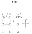
- FIG. 2 is a plan view schematically showing a planar pattern of the seed crystal film 3B on the substrate 1.
- FIG. 3 is a plan view schematically showing a planar pattern of the seed crystal film 3 ⁇ / b> C on the substrate 1.
- FIG. 4 is a plan view schematically showing a planar pattern of the seed crystal film 3A on the substrate 1.
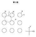
- FIG. 5 is a plan view schematically showing a planar pattern of the seed crystal film 3D on the substrate 1.
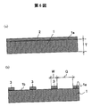
- FIG. 6A is a cross-sectional view schematically showing a state in which the seed crystal film 2 is formed on the surface 1a of the substrate 1, and FIG. 6B shows the seed crystal film 3 that is separated from each other. It is sectional drawing which shows a state typically.
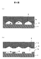
- FIG. 7A is a cross-sectional view schematically showing a state in which a group III metal nitride single crystal 4 is grown on the seed crystal film 3 of FIG. 6 by a flux method, and FIG. It is sectional drawing which shows typically the state which peeled the single crystal 4 from.
- FIG. 8A is a cross-sectional view schematically showing a state in which the seed crystal film 2 is formed on the surface 1a of the substrate 1, and FIG.
- FIG. 8B shows the recess 5 and the seed crystal film 3 separated from each other. It is sectional drawing which shows the formed state typically.
- FIG. 9A is a cross-sectional view schematically showing a state in which the group III metal nitride single crystal 4 is grown on the seed crystal film 3 of FIG. 8 by the flux method, and FIG. It is sectional drawing which shows typically the state which peeled the single crystal 4 from.
- a plurality of seed crystal films 3 ⁇ / b> A are formed on the surface of the substrate 1.
- the various crystal films 3A are separated from each other, and a non-film formation surface 1b is provided between adjacent seed crystal films 3A.
- the seed crystal films 3A are arranged at regular intervals in the horizontal direction X in FIG. 1, and are arranged at regular intervals in the oblique direction Y.
- a plurality of quadrilateral seed crystal films 3 ⁇ / b> B are formed on the surface of the substrate 1.
- the various crystal films 3B are separated from each other, and a non-film formation surface 1b is provided between adjacent seed crystal films 3B.
- the seed crystal films 3B are arranged at regular intervals in the horizontal direction X in FIG. 2 and are arranged at regular intervals in the vertical direction Y.
- a plurality of band-shaped or rectangular seed crystal films 3 ⁇ / b> C are formed on the surface of the substrate 1.
- the various crystal films 3C are separated from each other, and a non-film formation surface 1b is provided between adjacent seed crystal films 3C.
- the seed crystal films 3C are arranged at regular intervals in the horizontal direction X in FIG. 3, and are arranged at regular intervals in the vertical direction Y.
- a plurality of triangular seed crystal films 3 ⁇ / b> C are formed on the surface of the substrate 1.
- the various crystal films 3C are separated from each other, and a non-film formation surface 1b is provided between adjacent seed crystal films 3C.
- the seed crystal films 3C are arranged at regular intervals in the horizontal direction X in FIG. 4 and are arranged at regular intervals in the vertical direction Y.
- a plurality of circular seed crystal films 3 ⁇ / b> D are formed on the surface of the substrate 1.
- the various crystal films 3D are separated from each other, and a non-film formation surface 1b is provided between adjacent seed crystal films 3D.
- the seed crystal films 3D are arranged at regular intervals in the horizontal direction X in FIG.
- the seed crystal films are arranged in at least two directions X and Y.
- the X axis and the Y axis need only intersect (see FIG. 1), and do not need to be orthogonal as shown in FIGS.
- the angle of intersection between the X axis and the Y axis is preferably 40 to 140 °, and more preferably 45 to 135 °.
- the pitch of the seed crystal film is preferably constant, but it is not always necessary.
- the maximum inscribed circle diameter A of the seed crystal films 3A to 3D is 50 ⁇ m or more and 6 mm or less.
- the maximum inscribed circle diameter A of the seed crystal films 3A to 3D is less than 50 ⁇ m, when the group III metal nitride single crystal is grown by the flux method, the single crystal is formed thereon by meltback to the flux of the seed crystal film. Can no longer be grown, and a single self-supporting single crystal film cannot be obtained. From this viewpoint, it is more preferable that the maximum inscribed circle diameter A of the seed crystal films 3A to 3D is 100 ⁇ m or more. Such a problem does not occur when a group III metal nitride single crystal is formed by a vapor phase method. Rather, if A is large, an integral single crystal film cannot be formed.
- the maximum inscribed circle diameter A of the seed crystal films 3A to 3D exceeds 6 mm, a crack is generated in the grown single crystal.
- the maximum inscribed circle diameter A of the seed crystal films 3A to 3D is more preferably 1 mm or less, and even more preferably 500 ⁇ m or less.
- the circumscribed circle diameter B of the seed crystal films 3A to 3D is 50 ⁇ m or more and 10 mm or less.
- the circumscribed circle diameter B of the seed crystal films 3A to 3D is less than 50 ⁇ m, when the group III metal nitride single crystal is grown by the flux method, the single crystal is formed on the seed crystal film by meltback to the flux of the seed crystal film.
- the circumscribed circle diameter B of the seed crystal films 3A to 3D is 100 ⁇ m or more.
- the circumscribed circle diameter B of the seed crystal films 3A to 3D exceeds 10 mm, a crack is generated in the grown single crystal.
- the circumscribed circle diameter B of the seed crystal films 3A to 3D is more preferably 7 mm or less.
- the maximum inscribed circle diameter C of the non-growing surfaces of the seed crystal films 3A to 3D is 100 ⁇ m or more and 1 mm or less.
- the maximum inscribed circle diameter C of the non-growing surfaces of the seed crystal films 3A to 3D is less than 100 ⁇ m, cracks are likely to occur in the grown single crystal. From this viewpoint, it is more preferable that the maximum inscribed circle diameter C of the non-growth surfaces of the seed crystal films 3A to 3D is 200 ⁇ m or more. If the maximum inscribed circle diameter of the non-growing surfaces of the seed crystal films 3A to 3D exceeds 1 mm, the grown single crystal is likely to crack. From this viewpoint, it is more preferable that the maximum inscribed circle diameter of the non-growth surfaces of the seed crystal films 3A to 3D be 700 ⁇ m or less.
- the planar shape of the seed crystal film may be a curved shape such as a circle, an ellipse, or a racetrack, or a polygon such as a star, triangle, quadrilateral, or hexagon.
- a non-growth surface is a surface on which the single crystal 4 does not grow. Specifically, the non-growing surface is an exposed surface of the substrate or the surface of another film (for example, an oxide thin film layer) formed on the substrate. Next, the form of the seed crystal film and the non-growing surface will be illustrated. As shown in FIG. 6A, the surface 1a of the substrate 1 is processed smoothly, and a well-oriented seed crystal film 2 is formed on the surface 1a.
- the seed crystal film 2 is processed to form a plurality of seed crystal films 3 separated from each other as shown in FIG.
- a non-growing surface 1b is formed between adjacent seed crystal films 3.
- a group III metal nitride single crystal 4 is formed on the seed crystal film 3 by a flux method.
- the single crystals 4 formed on the adjacent seed crystal films 3 are connected to cover the substrate 1.
- the single crystal 4 is peeled from the template substrate naturally or with little effort, as shown in FIG. Extremely high. 8 and 9 show another embodiment. As shown in FIG.
- the surface 1a of the substrate 1 is processed smoothly, and the seed crystal film 2 is formed on the surface 1a.
- the surface 1a of the substrate 1 is processed to form a plurality of seed crystal films 3 spaced apart from each other as shown in FIG. 8B.
- the recess 5 is formed by further processing from the substrate surface 1a toward the inside. Therefore, the seed crystal film 3 remains on the protrusions 8 between the recesses 5.
- the film formation surface 1a remains and a side wall surface 8a is formed.
- the side wall surface 8a and the recess bottom surface 1b are processed surfaces formed by processing. Next, as shown in FIG.
- a group III metal nitride single crystal 4 is formed on the seed crystal film 3 by a flux method.
- the single crystals 4 formed on the adjacent seed crystal films 3 are connected to cover the substrate 1.
- the single crystal 4 is peeled off from the substrate 1 naturally or with little effort, so that productivity is improved.
- the thickness T (see FIGS. 6 and 8) of the substrate 1 is particularly preferably 0.8 mm or more and 1.2 mm or less, which can promote natural peeling from the single crystal substrate. From this viewpoint, the thickness T of the substrate is more preferably 0.9 mm or more, and further preferably 1.1 mm or less.
- the angle ⁇ formed by the longitudinal direction of the side wall surface 8a of the protrusion 8 and the a-axis of the substrate is 25 ° or less, more preferably 20 ° or less, and even more preferably 10 ° or less.
- the longitudinal direction of the side wall surface of the protrusion is parallel to the a-axis of the substrate body.
- the a-axis indicates ⁇ 1 1 -2 0> of a hexagonal single crystal.
- the material of the substrate is not particularly limited, but a perovskite type composite such as sapphire, silicon single crystal, SiC single crystal, MgO single crystal, spinel (MgAl 2 O 4 ), LiAlO 2 , LiGaO 2 , LaAlO 3 , LaGaO 3 , NdGaO 3, etc. An oxide can be illustrated.
- SCAM ScAlMgO 4
- the formation method of the non-growing surface 1b is not limited.
- a deep groove depth of 10 microns or more
- the processed surface is smooth, the processing strain remains, and is not epi-ready (that is, the surface state where the GaN thin film does not grow), for example, laser processing, plasma etching, dicing (diamond blade) may be used.
- the depth d of the recess 5 in FIGS. 8B and 9B is preferably 100 ⁇ m or less from the viewpoint of promoting the peeling of the grown single crystal and preventing the occurrence of cracks in the substrate 1 from the recess.
- the group III metal nitride single crystal constituting the seed crystal film is a nitride of one or more metals selected from Ga, Al, and In, such as GaN, AlN, GaAlN, and GaAlInN. Of these, GaN, AlN, and GaAlN are preferable.
- the formation method of the seed crystal film is preferably the MOCVD method from the viewpoint of controllability of impurity concentration and film thickness uniformity.
- the thickness of the seed crystal film is not particularly limited. From the viewpoint of suppressing the meltback of the seed crystal film, the thickness is preferably 1 ⁇ m or more, and more preferably 5 ⁇ m or more. In addition, when the base film is thick, it takes time to form the base film, so that the film thickness is preferably as thin as possible so as not to melt back. From this viewpoint, the thickness of the seed crystal film can be 30 ⁇ m or less.
- a group III metal nitride single crystal is grown on the seed crystal film by a flux method.
- the type of flux is not particularly limited as long as a group III metal nitride single crystal can be produced.
- a flux containing at least one of sodium metal and calcium metal is used, and a flux containing sodium metal is particularly preferred.
- the raw material of the target group III metal nitride single crystal is mixed and used.
- This group III metal nitride single crystal is a nitride of one or more metals selected from Ga, Al, In, and B, such as GaN, AlN, GaAlN, GaAlInN, and BN. GaN and GaAlN are preferable.
- the raw materials constituting the flux are selected according to the target group III metal nitride single crystal.
- gallium source material a gallium simple metal, a gallium alloy, and a gallium compound can be applied, but a gallium simple metal is also preferable in terms of handling.
- aluminum raw material an aluminum simple metal, an aluminum alloy, and an aluminum compound can be applied, but an aluminum simple metal is also preferable in terms of handling.
- indium raw material indium simple metal, indium alloy, and indium compound can be applied, but indium simple metal is preferable from the viewpoint of handling.
- the growth temperature of the group III metal nitride single crystal and the holding time during the growth are not particularly limited, and are appropriately changed according to the type of the desired group III metal nitride single crystal and the composition of the flux.
- the growth temperature can be set to 800 to 1000 ° C.
- the group III metal nitride single crystal is grown in an atmosphere composed of a mixed gas containing nitrogen gas.
- the total pressure of the atmosphere is not particularly limited, but is preferably 10 atm or more, and more preferably 30 atm or more from the viewpoint of preventing evaporation of the flux. However, since the apparatus becomes large when the pressure is high, the total pressure of the atmosphere is preferably 200 atm or less, and more preferably 100 atm or less.
- the nitrogen partial pressure in the atmosphere is not particularly limited, but when growing a gallium nitride single crystal, it is preferably 10 to 200 atm, more preferably 30 to 100 atm. When growing an aluminum nitride single crystal, the pressure is preferably 0.1 to 50 atm, and more preferably 1 to 10 atm.
- a gas other than nitrogen in the atmosphere is not limited, but an inert gas is preferable, and argon, helium, and neon are particularly preferable.
- the partial pressure of a gas other than nitrogen is a value obtained by subtracting the nitrogen gas partial pressure from the total pressure.
- the actual training method in the present invention is not particularly limited.
- the template substrate can be immersed in a flux in a crucible, the crucible can be accommodated in a pressure resistant container, and heated while supplying a nitrogen-containing atmosphere in the pressure resistant container.
- the flux can be brought into contact with the surface of the seed crystal film by fixing the template substrate at a predetermined position and raising the crucible containing the flux upward.
- Example 1 A gallium nitride single crystal was grown according to the method described with reference to FIGS. Specifically, a 70 nm GaN low-temperature buffer layer is first formed on the surface 1a of the c-plane sapphire substrate 1 having a diameter of 4 inches and a thickness of 0.8 mm at 550 ° C., and then a GaN thin film 2 having a thickness of 8 microns. Was formed at 1050 ° C. by a vapor phase method. The surface of this GaN template was processed by sandblasting. Processing was continued until the GaN thin film disappeared and the sapphire substrate surface was exposed, and the processing depth was 8 ⁇ m.
- the GaN thin film in the outer peripheral area of 1.5 mm was simultaneously removed by sandblasting.
- the planar shapes of the protrusions and seed crystal film 3D formed on the substrate were circular as shown in FIG. 5, and a large number of circular seed crystal films 3D were arranged in the X-axis and Y-axis directions.
- the maximum inscribed circle diameter A of the seed crystal film 3D was 50 ⁇ m
- the circumscribed circle diameter B was 50 ⁇ m
- the maximum inscribed circle diameter C of the non-growing surface was 500 ⁇ m.
- a gallium nitride single crystal was grown on the template substrate by a flux method.
- a ⁇ 4 inch GaN template grooved as a seed crystal substrate was placed at the center of the bottom in a growth vessel having an inner diameter of ⁇ 120 mm. Furthermore, 130 g of metallic sodium, 90 g of metallic gallium, and 350 mg of carbon were filled in the growth vessel.
- the growth vessel was placed in a refractory metal vessel and sealed, and then placed on a table where the crystal growth furnace can be swung and rotated. Crystals were grown by pressurizing to 4.5 MPa with nitrogen gas while raising the temperature to 870 ° C., and holding the flux solution for 100 hours while stirring by rocking and rotating. Thereafter, it was gradually cooled to room temperature over 30 hours.
- Example 2 In the same manner as in Example 1, a gallium nitride single crystal was grown. However, the seed crystal film 3C is configured as shown in FIG. 3, and a large number of rectangular seed crystal films 3C are arranged in the X-axis direction and the Y-axis direction.
- the inscribed circle diameter A of the seed crystal film 3C was 50 ⁇ m, the circumscribed circle diameter B was 10 mm, and the maximum inscribed circle diameter C of the non-growing surface 1b was 500 ⁇ m.
- the obtained gallium nitride crystal plate was detached from the entire surface of the sapphire substrate and became self-supporting, and there were no cracks. The diameter was 4 inches and the thickness was about 1.5 mm.
- Example 3 In the same manner as in Example 1, a gallium nitride single crystal was grown. However, the seed crystal film 3C is configured as shown in FIG. 3, and a large number of rectangular seed crystal films 3C are arranged in the X-axis direction and the Y-axis direction.
- the inscribed circle diameter A of the seed crystal film 3C was 6 mm, the circumscribed circle diameter B was 10 mm, and the maximum inscribed circle diameter C of the non-growing surface 1b was 500 ⁇ m.
- the obtained gallium nitride crystal plate was detached from the entire surface of the sapphire substrate and became self-supporting, and there were no cracks. The diameter was 4 inches and the thickness was about 1.5 mm.
- Example 4 In the same manner as in Example 1, a gallium nitride single crystal was grown. However, the seed crystal film 3C is configured as shown in FIG. 3, and a large number of rectangular seed crystal films 3C are arranged in the X-axis direction and the Y-axis direction.
- the inscribed circle diameter A of the seed crystal film 3C was 1 mm
- the circumscribed circle diameter B was 6 mm
- the maximum inscribed circle diameter C of the non-growing surface 1b was 500 ⁇ m.
- the obtained gallium nitride crystal plate was detached from the entire surface of the sapphire substrate and became self-supporting, and there were no cracks. The diameter was 4 inches and the thickness was about 1.5 mm.
- Example 5 In the same manner as in Example 1, a gallium nitride single crystal was grown. However, the seed crystal film 3C is configured as shown in FIG. 3, and a large number of rectangular seed crystal films 3C are arranged in the X-axis direction and the Y-axis direction.
- the inscribed circle diameter A of the seed crystal film 3C was 1 mm
- the circumscribed circle diameter B was 6 mm
- the maximum inscribed circle diameter C of the non-growing surface 1b was 100 ⁇ m.
- the obtained gallium nitride crystal plate was detached from the entire surface of the sapphire substrate and became self-supporting, and there were no cracks. The diameter was 4 inches and the thickness was about 1.5 mm.
- Example 6 In the same manner as in Example 1, a gallium nitride single crystal was grown. However, the seed crystal film 3C is configured as shown in FIG. 3, and a large number of rectangular seed crystal films 3C are arranged in the X-axis direction and the Y-axis direction.
- the inscribed circle diameter A of the seed crystal film 3C was 1 mm
- the circumscribed circle diameter B was 6 mm
- the maximum inscribed circle diameter C of the non-growing surface 1b was 1 mm.
- the obtained gallium nitride crystal plate was detached from the entire surface of the sapphire substrate and became self-supporting, and there were no cracks. The diameter was 4 inches and the thickness was about 1.5 mm.
- (Comparative Example 1) In the same manner as in Example 1, a gallium nitride single crystal was grown. However, the seed crystal film 3C is configured as shown in FIG. 3, and a large number of rectangular seed crystal films 3C are arranged in the X-axis direction and the Y-axis direction.
- the inscribed circle diameter A of the seed crystal film 3C was 10 ⁇ m, the circumscribed circle diameter B was 6 mm, and the maximum inscribed circle diameter C of the non-growing surface 1b was 500 ⁇ m.
- the GaN thin film part partially melted back, and the GaN crystal did not grow in the corresponding part.
- Comparative Example 2 In the same manner as in Example 1, a gallium nitride single crystal was grown. However, the seed crystal film 3C is configured as shown in FIG. 3, and a large number of rectangular seed crystal films 3C are arranged in the X-axis direction and the Y-axis direction.
- the inscribed circle diameter A of the seed crystal film 3C was 1 mm, the circumscribed circle diameter B was 15 mm, and the maximum inscribed circle diameter C of the non-growing surface 1b was 500 ⁇ m.
- the obtained gallium nitride crystal plate had a diameter of 4 inches and a thickness of about 1.5 mm, but cracks were found visually.
- Comparative Example 3 In the same manner as in Example 1, a gallium nitride single crystal was grown. However, the seed crystal film 3C is configured as shown in FIG. 3, and a large number of rectangular seed crystal films 3C are arranged in the X-axis direction and the Y-axis direction.
- the inscribed circle diameter A of the seed crystal film 3C was 1 mm
- the circumscribed circle diameter B was 6 mm
- the maximum inscribed circle diameter C of the non-growing surface 1b was 50 ⁇ m.
- the obtained gallium nitride crystal plate had a diameter of 4 inches and a thickness of about 1.5 mm, but cracks were found visually.
- Comparative Example 4 In the same manner as in Example 1, a gallium nitride single crystal was grown. However, the seed crystal film 3C is configured as shown in FIG. 3, and a large number of rectangular seed crystal films 3C are arranged in the X-axis direction and the Y-axis direction.
- the inscribed circle diameter A of the seed crystal film 3C was 1 mm
- the circumscribed circle diameter B was 6 mm
- the maximum inscribed circle diameter C of the non-growing surface 1b was 1.6 mm.
- the obtained gallium nitride crystal plate had a diameter of 4 inches and a thickness of about 1.5 mm, but cracks were found visually.
- Comparative Example 5 In the same manner as in Example 1, a gallium nitride single crystal was grown. However, the seed crystal film 3C is configured as shown in FIG. 3, and a large number of rectangular seed crystal films 3C are arranged in the X-axis direction and the Y-axis direction.
- the inscribed circle diameter A of the seed crystal film 3C was 8 mm, the circumscribed circle diameter B was 15 mm, and the maximum inscribed circle diameter C of the non-growing surface 1b was 500 ⁇ m.
- the obtained gallium nitride crystal plate had a diameter of 4 inches and a thickness of about 1.5 mm, but cracks were found visually.
- Tables 1, 2, and 3 below summarize the experimental results. However, the table shows the shape of the seed crystal film (circular, oval, rectangular) The results of each experiment shown in the table are as follows.
Landscapes
- Chemical & Material Sciences (AREA)
- Engineering & Computer Science (AREA)
- Crystallography & Structural Chemistry (AREA)
- Materials Engineering (AREA)
- Metallurgy (AREA)
- Organic Chemistry (AREA)
- Inorganic Chemistry (AREA)
- Crystals, And After-Treatments Of Crystals (AREA)
- Liquid Deposition Of Substances Of Which Semiconductor Devices Are Composed (AREA)
- Semiconductor Lasers (AREA)
Abstract
Description
特開2004−247711では、テンプレート基板の表面に凹凸形状を形成したものを種基板として用い、Naフラックス法にてGaNを結晶成長させた後、凹部に形成された空隙部の近傍でフラックス法成長部分をテンプレートから分離(剥離)している。
特開2005−12171では、テンプレート基板の表面に種結晶膜に間隙を設け、種結晶上にフラックス法によってIII族金属窒化物単結晶を成長させている。
また、特開2008−239365では、サファイア基板の表面に島状部を加工によって形成し、島状部の表面に種結晶膜を形成し、種結晶膜上にIII族金属窒化物単結晶をフラックス法によって形成することが記載されている。
特開2009−120465では、下地基板上に幅(あるいは直径)10~100μmのマスクを250~2000μmの間隔で形成し、ついで基板上に気相成長法でGaN結晶を成長させている。
特開2004−182551では、多数の種結晶部分を下地基板の表面に形成し、ついで気相法によって窒化ガリウム単結晶を育成している。
特開2001−267243の図11および(0058)では、基板上に島状の段差を多数形成し、その上にIII族金属窒化物単結晶を気相法で成膜している。
しかし、本発明者が更に検討した結果、III族金属窒化物単結晶をフラックス法で成長させて冷却したときに、単結晶が基板から剥離しないことが多く、特に単結晶の全面にわたって剥離させることは困難であった。また、育成したIII族金属窒化物単結晶にクラックが入りやすく、不良の原因となっていた。
本発明の課題は、基板上に複数の種結晶膜を成膜し、種結晶膜上にフラックス法によってIII族金属窒化物単結晶を育成するのに際して、育成した単結晶の基板からの剥離を容易にし、かつ単結晶中のクラックを抑制することである。
本発明は、基板上にIII族金属窒化物単結晶の複数の種結晶膜を成膜し、この際基板に種結晶膜によって被覆されていない非育成面を形成する種結晶膜作製工程;および
種結晶膜上にフラックス法によってIII族金属窒化物単結晶を育成する育成工程;
を有する方法であって、
複数の種結晶膜が互いに非育成面によって分けられており、かつ少なくとも二方向へと向かって配列されており、種結晶膜の最大内接円径が50μm以上、6mm以下であり、種結晶膜の外接円径が50μm以上、10mm以下であり、非育成面の最大内接円径が100μm以上、1mm以下であることを特徴とする。
本発明によれば、フラックス法で育成したIII族金属窒化物単結晶の基板からの剥離が促進され、自然剥離も容易に起こるようになった。これに加えて、育成した単結晶中のクラックが抑制されることがわかった。
特開2004−247711、特開2005−12171、特開2008−239365では、本発明のように少なくとも二方向へと向かって種結晶膜を配列する形態が記載されていない。
特開2009−120465、特開2004−182551、特開2001−267243では、III族金属窒化物単結晶を気相法によって形成する。このため、種結晶膜の幅、隣接する種結晶膜の間隔は、いずれも1μmあるいはその近傍である必要があり、これ以上種結晶膜の幅や間隔が大きいと、一体の成膜は無理であるので、本発明とは根本的に異なる。
図2は、基板1上の種結晶膜3Bの平面的パターンを模式的に示す平面図である。
図3は、基板1上の種結晶膜3Cの平面的パターンを模式的に示す平面図である。
図4は、基板1上の種結晶膜3Aの平面的パターンを模式的に示す平面図である。
図5は、基板1上の種結晶膜3Dの平面的パターンを模式的に示す平面図である。
図6(a)は、基板1の表面1a上に種結晶膜2を形成した状態を模式的に示す断面図であり、図6(b)は、互いに離間された種結晶膜3を形成した状態を模式的に示す断面図である。
図7(a)は、図6の種結晶膜3上にIII族金属窒化物単結晶4をフラックス法で育成した状態を模式的に示す断面図であり、図7(b)は、基板1から単結晶4を剥離させた状態を模式的に示す断面図である。
図8(a)は、基板1の表面1aに種結晶膜2を形成した状態を模式的に示す断面図であり、図8(b)は、凹部5および互いに離間された種結晶膜3を形成した状態を模式的に示す断面図である。
図9(a)は、図8の種結晶膜3上にIII族金属窒化物単結晶4をフラックス法で育成した状態を模式的に示す断面図であり、図9(b)は、基板1から単結晶4を剥離させた状態を模式的に示す断面図である。
本発明では、例えば図1に示すように、基板1の表面に複数の種結晶膜3Aを形成する。各種結晶膜3Aは互いに離間されており、隣接する種結晶膜3Aの間には非成膜面1bが設けられている。種結晶膜3Aは、図1において水平方向Xへと向かって一定間隔で配列されており、かつ、斜め方向Yへと向かって一定間隔で配列されている。
図2の例では、基板1の表面に複数の四辺形の種結晶膜3Bを形成する。各種結晶膜3Bは互いに離間されており、隣接する種結晶膜3Bの間には非成膜面1bが設けられている。種結晶膜3Bは、図2において水平方向Xへと向かって一定間隔で配列されており、かつ、上下方向Yへと向かって一定間隔で配列されている。
図3の例では、基板1の表面に複数の帯状ないし矩形の種結晶膜3Cを形成する。各種結晶膜3Cは互いに離間されており、隣接する種結晶膜3Cの間には非成膜面1bが設けられている。種結晶膜3Cは、図3において水平方向Xへと向かって一定間隔で配列されており、かつ、上下方向Yへと向かって一定間隔で配列されている。
図4の例では、基板1の表面に複数の三角形の種結晶膜3Cを形成する。各種結晶膜3Cは互いに離間されており、隣接する種結晶膜3Cの間には非成膜面1bが設けられている。種結晶膜3Cは、図4において水平方向Xへと向かって一定間隔で配列されており、かつ、上下方向Yへと向かって一定間隔で配列されている。
図5の例では、基板1の表面に複数の円形の種結晶膜3Dを形成する。各種結晶膜3Dは互いに離間されており、隣接する種結晶膜3Dの間には非成膜面1bが設けられている。種結晶膜3Dは、図5において水平方向Xへと向かって一定間隔で配列されており、かつ、上下方向Yへと向かって一定間隔で配列されている。
本発明においては、種結晶膜が、少なくとも2方向X、Yに向かって配列されている。ここで、X軸とY軸とは、交差していればよく(図1参照)、図2~図5のように直交している必要はない。ただし、X軸とY軸との交差角度は、40~140°が好ましく、45~135°が更に好ましい。
X軸方向、Y軸方向において、それぞれ、種結晶膜のピッチは、一定であることが好ましいが、必ずしも一定であることは必須ではない。
本発明においては、種結晶膜3A~3Dの最大内接円径Aが50μm以上、6mm以下である。
種結晶膜3A~3Dの最大内接円径Aが50μm未満になると、フラックス法によってIII族金属窒化物単結晶を育成するときに、種結晶膜のフラックスへのメルトバックによってその上に単結晶が育成されなくなり、一体の自立した単結晶膜を得ることができない。この観点からは、種結晶膜3A~3Dの最大内接円径Aを100μm以上とすることが更に好ましい。III族金属窒化物単結晶を気相法によって形成する場合には、このような問題点は生じず、むしろAが大きいと一体の単結晶膜を形成することはできない。
種結晶膜3A~3Dの最大内接円径Aが6mmを超えると、育成された単結晶にクラックが発生する。この観点からは、種結晶膜3A~3Dの最大内接円径Aが1mm以下であることが更に好ましく、500μm以下であることがよりいっそう好ましい。
また,本発明では、種結晶膜3A~3Dの外接円径Bが50μm以上、10mm以下である。
種結晶膜3A~3Dの外接円径Bが50μm未満であると、フラックス法によってIII族金属窒化物単結晶を育成するときに、種結晶膜のフラックスへのメルトバックによってその上に単結晶が育成されなくなり、一体の自立した単結晶膜を得ることができない。この観点からは、種結晶膜3A~3Dの外接円径Bを100μm以上とすることが更に好ましい。
種結晶膜3A~3Dの外接円径Bが10mmを超えると育成された単結晶にクラックが発生する。この観点からは、種結晶膜3A~3Dの外接円径Bが7mm以下であることが更に好ましい。
また、本発明では、種結晶膜3A~3Dの非育成面の最大内接円径Cが100μm以上、1mm以下である。種結晶膜3A~3Dの非育成面の最大内接円径Cが100μm未満であると、育成された単結晶にクラックが発生しやすい。この観点からは、種結晶膜3A~3Dの非育成面の最大内接円径Cを200μm以上とすることが更に好ましい。
種結晶膜3A~3Dの非育成面の最大内接円径が1mmを超えると、育成された単結晶にクラックが発生しやすい。この観点からは、種結晶膜3A~3Dの非育成面の最大内接円径を700μm以下とすることが更に好ましい。
種結晶膜の平面形状は、円形、楕円形、レーストラック形状などの湾曲形状、星形、三角形、四辺形、六角形などの多角形であってよい。
非育成面とは、単結晶4が成長しない面である。具体的には、非育成面は、基板の露出面であり、あるいは、基板上に成膜された他の膜(例えば酸化物薄膜層)の表面である。
次に、種結晶膜および非育成面の形態について例示する。
図6(a)に示すように、基板1の表面1aは平滑に加工されており、表面1a上に、よく配向された種結晶膜2が形成されている。
次いで、種結晶膜2を加工し、図6(b)に示すように、互いに離間された複数の種結晶膜3を形成する。隣接する種結晶膜3の間には非育成面1bが形成されている。
次に、図7(a)に示すように、種結晶膜3上にフラックス法によってIII族金属窒化物単結晶4を形成する。この工程では、隣接する種結晶膜3上に形成された各単結晶4がつながり、基板1を被覆していく。
次いで、単結晶4の成長後の降温過程において、図7(b)に示すように、単結晶4が基板1から、自然に、あるいは少ない労力をもって容易にテンプレート基板から剥離するので、生産性がきわめて高くなる。
図8、図9は他の実施形態を示すものである。図8(a)に示すように、基板1の表面1aは平滑に加工されており、表面1aに種結晶膜2が形成されている。次いで、基板1の表面1aを加工し、図8(b)に示すように、互いに離間された複数の種結晶膜3を形成する。ただし、本例では、基板表面1aから内側へと向かって更に加工し、凹部5を形成する。従って、種結晶膜3は、凹部5間の突起8上に残留することになる。突起8には、成膜面1aが残留するとともに、側壁面8aが形成される。側壁面8aおよび凹部底面1bは、加工によって形成された加工面である。
次に、図9(a)に示すように、種結晶膜3上にフラックス法によってIII族金属窒化物単結晶4を形成する。この工程では、隣接する種結晶膜3上に形成された各単結晶4がつながり、基板1を被覆していく。
次いで、単結晶4の成長後の降温過程において、図9(b)に示すように、単結晶4が基板1から、自然に、あるいは少ない労力をもって容易にテンプレート基板から剥離するので、生産性がきわめて高くなる。
基板1の厚さT(図6、図8参照)は0.8mm以上、1.2mm以下とすることが特に好ましく、これによって単結晶の基板からの自然剥離を促進できる。この観点からは、基板の厚さTは、0.9mm以上とすることが更に好ましく、また、1.1mm以下とすることが更に好ましい。
好ましくは、突起8の側壁面8aの長手方向と基板のa軸とがなす角度θが25°以下であり、更に好ましくは20°以下であり、一層好ましくは10°以下である。最も好ましくは、突起の側壁面の長手方向と基板本体のa軸とが平行である。
ここで、a軸とは、六方晶単結晶の<1 1 −2 0>を示す。サファイア、窒化ガリウムともに、六方晶系なので、a1、a2、a3は等価であり、[2 −1 −1 0]、[1 1 −2 0]、[−1 2 −1 0]、[−21 1 0]、[−1 −1 2 0]、[1 −2 1 0]の6つは等価である。この6つのうち、a軸は慣例で[1 1 −2 0]を用いることが多く、本願でいうa軸はこのすべての等価な軸のことを意味し、[1 1 −2 0]と表記する場合でも、前記等価な軸をすべて含む。
基板の材質は特に限定されないが、サファイア、シリコン単結晶、SiC単結晶、MgO単結晶、スピネル(MgAl2O4)、LiAlO2、LiGaO2、LaAlO3,LaGaO3,NdGaO3等のペロブスカイト型複合酸化物を例示できる。また組成式
〔A1−y(Sr1−xBax)y〕〔(Al1−zGaz)1−u・Du〕O3
(Aは、希土類元素である;Dは、ニオブおよびタンタルからなる群より選ばれた一種以上の元素である;y=0.3~0.98;x=0~1;z=0~1;u=0.15~0.49;x+z=0.1~2)の立方晶系のペロブスカイト構造複合酸化物も使用できる。また、SCAM(ScAlMgO4)も使用できる。
非育成面1bの形成方法は限定されない。特に、サンドブラストにより、溝入れ加工することで、低コストかつリソグラフィでは作製困難な深い溝(10ミクロン以上の深さ)を作製することができる。また、加工面が平滑かつ、加工歪みが残存し、エピレディで無ければ(すなわちGaN薄膜が成長しない表面状態であれば)良く、例えば、レーザー加工でもよく、プラズマエッチング、ダイシング(ダイヤモンドブレード)でもよい。
図8(b)及び図9(b)の凹部5の深さdは、育成単結晶の剥離を促進し、凹部からの基板1のクラック発生を防止するという観点からは、100μm以下が好ましく、1μm以下がさらに好ましく、0.1μm以下が最も好ましい。サンドブラスト加工において、600~800番のアルミナ砥粒を用いると、サファイア基板の加工速度がGaN薄膜に比べて数10倍遅く、凹部深さの調整に好適である。
種結晶膜を構成するIII族金属窒化物単結晶は、Ga、Al、Inから選ばれた一種以上の金属の窒化物であり、GaN、AlN、GaAlN,GaAlInN等である。好ましくはGaN、AlN、GaAlNである。
種結晶膜の形成方法は、不純物濃度の制御性や膜厚均一性の観点からMOCVD法が好ましい。
種結晶膜の厚さは特に限定されない。種結晶膜のメルトバックを抑制するという観点からは、1μm以上であることが好ましく、5μm以上であることがさらに好ましい。また、下地膜を厚くすると、下地膜の形成に時間がかかるので、メルトバックしない程度のなるべく薄い膜厚が好ましい。この観点からは、種結晶膜の厚さを30μm以下とすることができる。
次いで、種結晶膜上にフラックス法によってIII族金属窒化物単結晶を育成する。
フラックスの種類は、III族金属窒化物単結晶を生成可能である限り、特に限定されない。好適な実施形態においては、ナトリウム金属とカルシウム金属との少なくとも一方を含むフラックスを使用し、ナトリウム金属を含むフラックスが特に好ましい。
フラックスには、目的とするIII族金属窒化物単結晶の原料を混合し、使用する。このIII族金属窒化物単結晶は、Ga、Al、In、Bから選ばれた一種以上の金属の窒化物であり、GaN、AlN、GaAlN,GaAlInN、BN等である。好ましくはGaN、GaAlNである。
フラックスを構成する原料は、目的とするIII族金属窒化物単結晶に合わせて選択する。
ガリウム原料物質としては、ガリウム単体金属、ガリウム合金、ガリウム化合物を適用できるが、ガリウム単体金属が取扱いの上からも好適である。
アルミニウム原料物質としては、アルミニウム単体金属、アルミニウム合金、アルミニウム化合物を適用できるが、アルミニウム単体金属が取扱いの上からも好適である。
インジウム原料物質としては、インジウム単体金属、インジウム合金、インジウム化合物を適用できるが、インジウム単体金属が取扱いの上からも好適である。
III族金属窒化物単結晶の育成温度や育成時の保持時間は特に限定されず、目的とするIII族金属窒化物単結晶の種類やフラックスの組成に応じて適宜変更する。一例では、ナトリウムまたはリチウム含有フラックスを用いて窒化ガリウム単結晶を育成する場合には、育成温度を800~1000℃とすることができる。
好適な実施形態においては、窒素ガスを含む混合ガスからなる雰囲気下でIII族金属窒化物単結晶を育成する。雰囲気の全圧は特に限定されないが、フラックスの蒸発を防止する観点からは、10気圧以上が好ましく、30気圧以上が更に好ましい。ただし、圧力が高いと装置が大がかりとなるので、雰囲気の全圧は、200気圧以下が好ましく、100気圧以下が更に好ましい。
また、雰囲気中の窒素分圧も特に限定されないが、窒化ガリウム単結晶を育成する場合には10~200気圧が好ましく、30~100気圧が更に好ましい。窒化アルミニウム単結晶を育成する場合には、0.1~50気圧が好ましく、1~10気圧が更に好ましい。
雰囲気中の窒素以外のガスは限定されないが、不活性ガスが好ましく、アルゴン、ヘリウム、ネオンが特に好ましい。窒素以外のガスの分圧は、全圧から窒素ガス分圧を除いた値である。
本発明における実際の育成手法は特に限定されない。例えばるつぼ内でテンプレート基板をフラックス中に浸漬し、るつぼを耐圧容器に収容し、耐圧容器内に窒素含有雰囲気を供給しつつ加熱できる。また、テンプレート基板を所定位置に固定し、フラックスが収容されたルツボを上方向へと上昇させることにより、種結晶膜の表面にフラックスを接触させることができる。
図8および図9を参照しつつ説明した方法に従い、窒化ガリウム単結晶を育成した。
具体的には、直径4インチ、厚さ0.8mmのc面サファイア基板1の表面1aに、まず550℃にてGaN低温バッファ層を70nm成膜し、その後、厚さ8ミクロンのGaN薄膜2を1050℃にて気相法により成膜した。このGaNテンプレートの表面をサンドブラストにより加工した。加工はGaN薄膜がなくなりサファイア基板面が露出するまでおこない、加工深さは8μmとした。また、外周部1.5mmの領域のGaN薄膜も同時にサンドブラストにより除去加工した。
ただし、基板に形成される突起および種結晶膜3Dの平面形状は、図5に示すような円形とし、円形の種結晶膜3DがX軸およびY軸方向に多数配列されるようにした。種結晶膜3Dの最大内接円径Aは50μmとし、外接円径Bは50μmとし、非育成面の最大内接円径Cは500μmとした。
次いで、フラックス法によって、テンプレート基板上に窒化ガリウム単結晶を育成した。具体的には、まず、アルゴン雰囲気のグローブボックス内で、内径φ120mmの育成容器内の底の中央に種結晶基板として溝加工したφ4インチGaNテンプレートを配置した。さらに金属ナトリウム130g、金属ガリウム90g、炭素350mgを育成容器内に充填した。この育成容器を耐熱金属製の容器に入れて密閉した後、結晶育成炉の揺動および回転が可能な台上に設置した。870℃に昇温しながら窒素ガスで4.5MPaに加圧、フラックス溶液を揺動および回転で撹拌しながら100時間保持することにより結晶成長させた。その後30時間かけて室温まで徐冷した。その後、結晶育成炉から育成容器を取り出し、エタノールを用いて、フラックスを除去し、成長した窒化ガリウム結晶板を回収した。
得られた窒化ガリウム結晶板は、サファイア基板と全面剥離し、自立化しており、クラックはなかった。直径はφ4インチであり、厚さは約1.5mmであった。
(実施例2)
実施例1と同様にして、窒化ガリウム単結晶を育成した。ただし、種結晶膜3Cの形態は図3に示すようにし、矩形の種結晶膜3CをX軸方向およびY軸方向に多数配列した。種結晶膜3Cの内接円径Aを50μmとし、外接円径Bを10mmとし、非育成面1bの最大内接円径Cを500μmとした。
得られた窒化ガリウム結晶板は、サファイア基板と全面剥離し、自立化しており、クラックはなかった。直径はφ4インチであり、厚さは約1.5mmであった。
(実施例3)
実施例1と同様にして、窒化ガリウム単結晶を育成した。ただし、種結晶膜3Cの形態は図3に示すようにし、矩形の種結晶膜3CをX軸方向およびY軸方向に多数配列した。種結晶膜3Cの内接円径Aを6mmとし、外接円径Bを10mmとし、非育成面1bの最大内接円径Cを500μmとした。
得られた窒化ガリウム結晶板は、サファイア基板と全面剥離し、自立化しており、クラックはなかった。直径はφ4インチであり、厚さは約1.5mmであった。
(実施例4)
実施例1と同様にして、窒化ガリウム単結晶を育成した。ただし、種結晶膜3Cの形態は図3に示すようにし、矩形の種結晶膜3CをX軸方向およびY軸方向に多数配列した。種結晶膜3Cの内接円径Aを1mmとし、外接円径Bを6mmとし、非育成面1bの最大内接円径Cを500μmとした。
得られた窒化ガリウム結晶板は、サファイア基板と全面剥離し、自立化しており、クラックはなかった。直径はφ4インチであり、厚さは約1.5mmであった。
(実施例5)
実施例1と同様にして、窒化ガリウム単結晶を育成した。ただし、種結晶膜3Cの形態は図3に示すようにし、矩形の種結晶膜3CをX軸方向およびY軸方向に多数配列した。種結晶膜3Cの内接円径Aを1mmとし、外接円径Bを6mmとし、非育成面1bの最大内接円径Cを100μmとした。
得られた窒化ガリウム結晶板は、サファイア基板と全面剥離し、自立化しており、クラックはなかった。直径はφ4インチであり、厚さは約1.5mmであった。
(実施例6)
実施例1と同様にして、窒化ガリウム単結晶を育成した。ただし、種結晶膜3Cの形態は図3に示すようにし、矩形の種結晶膜3CをX軸方向およびY軸方向に多数配列した。種結晶膜3Cの内接円径Aを1mmとし、外接円径Bを6mmとし、非育成面1bの最大内接円径Cを1mmとした。
得られた窒化ガリウム結晶板は、サファイア基板と全面剥離し、自立化しており、クラックはなかった。直径はφ4インチであり、厚さは約1.5mmであった。
(比較例1)
実施例1と同様にして、窒化ガリウム単結晶を育成した。ただし、種結晶膜3Cの形態は図3に示すようにし、矩形の種結晶膜3CをX軸方向およびY軸方向に多数配列した。種結晶膜3Cの内接円径Aを10μmとし、外接円径Bを6mmとし、非育成面1bの最大内接円径Cを500μmとした。
この結果、GaN薄膜部が部分的にメルトバックしており、該当部でGaN結晶が成長していなかった。
(比較例2)
実施例1と同様にして、窒化ガリウム単結晶を育成した。ただし、種結晶膜3Cの形態は図3に示すようにし、矩形の種結晶膜3CをX軸方向およびY軸方向に多数配列した。種結晶膜3Cの内接円径Aを1mmとし、外接円径Bを15mmとし、非育成面1bの最大内接円径Cを500μmとした。
得られた窒化ガリウム結晶板は、直径はφ4インチであり、厚さは約1.5mmであったが、目視でクラックがみとめられた。
(比較例3)
実施例1と同様にして、窒化ガリウム単結晶を育成した。ただし、種結晶膜3Cの形態は図3に示すようにし、矩形の種結晶膜3CをX軸方向およびY軸方向に多数配列した。種結晶膜3Cの内接円径Aを1mmとし、外接円径Bを6mmとし、非育成面1bの最大内接円径Cを50μmとした。
得られた窒化ガリウム結晶板は、直径はφ4インチであり、厚さは約1.5mmであったが、目視でクラックがみとめられた。
(比較例4)
実施例1と同様にして、窒化ガリウム単結晶を育成した。ただし、種結晶膜3Cの形態は図3に示すようにし、矩形の種結晶膜3CをX軸方向およびY軸方向に多数配列した。種結晶膜3Cの内接円径Aを1mmとし、外接円径Bを6mmとし、非育成面1bの最大内接円径Cを1.6mmとした。
得られた窒化ガリウム結晶板は、直径はφ4インチであり、厚さは約1.5mmであったが、目視でクラックがみとめられた。
(比較例5)
実施例1と同様にして、窒化ガリウム単結晶を育成した。ただし、種結晶膜3Cの形態は図3に示すようにし、矩形の種結晶膜3CをX軸方向およびY軸方向に多数配列した。種結晶膜3Cの内接円径Aを8mmとし、外接円径Bを15mmとし、非育成面1bの最大内接円径Cを500μmとした。
得られた窒化ガリウム結晶板は、直径はφ4インチであり、厚さは約1.5mmであったが、目視でクラックがみとめられた。
以下の表1、2、3に実験結果をまとめて示す。
ただし、表には、種結晶膜の形状を示す(円形、楕円、矩形)
また、表に示した各実験結果は以下のとおりである。
「○」 :GaN結晶板が自立化し、クラックなし
「クラック」 :GaN結晶板にクラック発生
「メルトバック」 :結晶育成時にGaN薄膜がメルトバック
「実・比」 :実施例・比較例該当結果


Claims (12)
- 基板上にIII族金属窒化物単結晶の複数の種結晶膜を成膜し、この際基板に前記種結晶膜によって被覆されていない非育成面を形成する種結晶膜作製工程;および
前記種結晶膜上にフラックス法によってIII族金属窒化物単結晶を育成する育成工程;
を有する方法であって、
前記複数の種結晶膜が互いに前記非育成面によって分けられており、かつ少なくとも二方向に向かって配列されており、前記種結晶膜の最大内接円径が50μm以上、6mm以下であり、前記種結晶膜の外接円径が50μm以上、10mm以下であり、前記非育成面の最大内接円径が100μm以上、1mm以下であることを特徴とする、III族金属窒化物単結晶の製造方法。 - 前記種結晶膜の最大内接円径が50μm以上、1mm以下であり、前記種結晶膜の外接円径が50μm以上、10mm以下であり、前記非育成面の最大内接円径が200μm以上、1mm以下であることを特徴とする、請求項1記載の方法。
- 前記種結晶膜の最大内接円径が50μm以上、500μm以下であり、前記種結晶膜の外接円径が50μm以上、10mm以下であり、前記非育成面の最大内接円径が200μm以上、1mm以下であることを特徴とする、請求項1記載の方法。
- 前記基板に凹部が形成されており、この凹部に前記非育成面が形成されていることを特徴とする、請求項1~3のいずれか一つの請求項に記載の方法。
- 前記種結晶膜の一つ以上が三角形ないし略三角形であることを特徴とする、請求項1~4のいずれか一つの請求項に記載の方法。
- 前記種結晶膜の一つ以上が四辺形ないし略四辺形であることを特徴とする、請求項1~4のいずれか一つの請求項に記載の方法。
- 前記種結晶膜の一つ以上が円形ないし略円形であることを特徴とする、請求項1~4のいずれか一つの請求項に記載の方法。
- 前記種結晶膜の一つ以上が楕円形ないし略楕円形であることを特徴とする、請求項1~4のいずれか一つの請求項に記載の方法。
- 前記育成工程において、隣接する前記種結晶膜から成長するIII族金属窒化物単結晶のa面同士を互いに会合させることを特徴とする、請求項1~8のいずれか一つの請求項に記載の方法。
- 育成される前記III族金属窒化物単結晶が、窒化ガリウム単結晶または窒化アルミニウム単結晶であることを特徴とする、請求項1~9のいずれか一つの請求項に記載の方法。
- 前記種結晶膜を構成する前記III族金属窒化物単結晶が、窒化ガリウム単結晶、窒化アルミニウム単結晶または窒化アルミニウム−窒化ガリウム固溶体結晶であることを特徴とする、請求項1~10のいずれか一つの請求項に記載の方法。
- 前記育成されたIII族金属窒化物単結晶を前記種結晶膜から自然剥離させることを特徴とする、請求項1~11のいずれか一つの請求項に記載の方法。
Priority Applications (3)
| Application Number | Priority Date | Filing Date | Title |
|---|---|---|---|
| JP2011521982A JPWO2011004904A1 (ja) | 2009-07-07 | 2010-07-06 | Iii族金属窒化物単結晶の製造方法 |
| CN201080030599.3A CN102471920B (zh) | 2009-07-07 | 2010-07-06 | Iii族金属氮化物单晶的制造方法 |
| US13/344,809 US20120111264A1 (en) | 2009-07-07 | 2012-01-06 | Method for producing group iii metal nitride single crystal |
Applications Claiming Priority (2)
| Application Number | Priority Date | Filing Date | Title |
|---|---|---|---|
| JP2009-161000 | 2009-07-07 | ||
| JP2009161000 | 2009-07-07 |
Related Child Applications (1)
| Application Number | Title | Priority Date | Filing Date |
|---|---|---|---|
| US13/344,809 Continuation US20120111264A1 (en) | 2009-07-07 | 2012-01-06 | Method for producing group iii metal nitride single crystal |
Publications (1)
| Publication Number | Publication Date |
|---|---|
| WO2011004904A1 true WO2011004904A1 (ja) | 2011-01-13 |
Family
ID=43429325
Family Applications (1)
| Application Number | Title | Priority Date | Filing Date |
|---|---|---|---|
| PCT/JP2010/061740 Ceased WO2011004904A1 (ja) | 2009-07-07 | 2010-07-06 | Iii族金属窒化物単結晶の製造方法 |
Country Status (4)
| Country | Link |
|---|---|
| US (1) | US20120111264A1 (ja) |
| JP (1) | JPWO2011004904A1 (ja) |
| CN (1) | CN102471920B (ja) |
| WO (1) | WO2011004904A1 (ja) |
Cited By (6)
| Publication number | Priority date | Publication date | Assignee | Title |
|---|---|---|---|---|
| JP2012197194A (ja) * | 2011-03-18 | 2012-10-18 | Ricoh Co Ltd | 13族窒化物結晶の製造方法、13族窒化物結晶基板の製造方法、13族窒化物結晶および13族窒化物結晶基板 |
| JP2014055091A (ja) * | 2012-09-13 | 2014-03-27 | Osaka Univ | Iii−v族化合物結晶製造方法、種結晶形成基板製造方法、iii−v族化合物結晶、半導体装置、iii−v族化合物結晶製造装置、種結晶形成基板製造装置 |
| KR20140097423A (ko) * | 2012-01-11 | 2014-08-06 | 고꾸리쯔 다이가꾸 호우징 오사까 다이가꾸 | Iii족 질화물 결정의 제조 방법, iii족 질화물 결정 및 반도체 장치 |
| US9065012B2 (en) | 2012-08-06 | 2015-06-23 | Ngk Insulators, Ltd. | Composite substrates and functional devices |
| WO2015159342A1 (ja) * | 2014-04-14 | 2015-10-22 | 株式会社サイオクス | 窒化物半導体単結晶基板の製造方法 |
| US10032958B2 (en) | 2012-12-20 | 2018-07-24 | Ngk Insulators, Ltd. | Seed crystal substrates, composite substrates and functional devices |
Families Citing this family (3)
| Publication number | Priority date | Publication date | Assignee | Title |
|---|---|---|---|---|
| CN107292394A (zh) * | 2016-04-11 | 2017-10-24 | 富泰华工业(深圳)有限公司 | 车辆损伤定价系统及方法 |
| US10304740B2 (en) * | 2016-12-15 | 2019-05-28 | Panasonic Intellectual Property Management Co., Ltd. | RAMO4 monocrystalline substrate |
| CN107123589B (zh) * | 2017-06-26 | 2020-01-07 | 镓特半导体科技(上海)有限公司 | 半导体结构、自支撑氮化镓层及其制备方法 |
Citations (2)
| Publication number | Priority date | Publication date | Assignee | Title |
|---|---|---|---|---|
| JP2005012171A (ja) * | 2003-03-20 | 2005-01-13 | Matsushita Electric Ind Co Ltd | Iii族窒化物基板の製造方法および半導体装置 |
| JP2009029639A (ja) * | 2007-06-25 | 2009-02-12 | Sumitomo Electric Ind Ltd | Iii族窒化物結晶の製造方法、iii族窒化物結晶基板およびiii族窒化物半導体デバイス |
Family Cites Families (6)
| Publication number | Priority date | Publication date | Assignee | Title |
|---|---|---|---|---|
| JP2001267691A (ja) * | 2000-01-13 | 2001-09-28 | Sony Corp | 半導体素子およびその製造方法 |
| JP3988018B2 (ja) * | 2001-01-18 | 2007-10-10 | ソニー株式会社 | 結晶膜、結晶基板および半導体装置 |
| JP3870869B2 (ja) * | 2002-07-24 | 2007-01-24 | 日亜化学工業株式会社 | 窒化物半導体基板の製造方法 |
| US7524691B2 (en) * | 2003-01-20 | 2009-04-28 | Panasonic Corporation | Method of manufacturing group III nitride substrate |
| US7176115B2 (en) * | 2003-03-20 | 2007-02-13 | Matsushita Electric Industrial Co., Ltd. | Method of manufacturing Group III nitride substrate and semiconductor device |
| JP2005057220A (ja) * | 2003-08-07 | 2005-03-03 | Sony Corp | 半導体光素子及びその製造方法 |
-
2010
- 2010-07-06 WO PCT/JP2010/061740 patent/WO2011004904A1/ja not_active Ceased
- 2010-07-06 JP JP2011521982A patent/JPWO2011004904A1/ja active Pending
- 2010-07-06 CN CN201080030599.3A patent/CN102471920B/zh not_active Expired - Fee Related
-
2012
- 2012-01-06 US US13/344,809 patent/US20120111264A1/en not_active Abandoned
Patent Citations (2)
| Publication number | Priority date | Publication date | Assignee | Title |
|---|---|---|---|---|
| JP2005012171A (ja) * | 2003-03-20 | 2005-01-13 | Matsushita Electric Ind Co Ltd | Iii族窒化物基板の製造方法および半導体装置 |
| JP2009029639A (ja) * | 2007-06-25 | 2009-02-12 | Sumitomo Electric Ind Ltd | Iii族窒化物結晶の製造方法、iii族窒化物結晶基板およびiii族窒化物半導体デバイス |
Cited By (13)
| Publication number | Priority date | Publication date | Assignee | Title |
|---|---|---|---|---|
| JP2012197194A (ja) * | 2011-03-18 | 2012-10-18 | Ricoh Co Ltd | 13族窒化物結晶の製造方法、13族窒化物結晶基板の製造方法、13族窒化物結晶および13族窒化物結晶基板 |
| US9834859B2 (en) | 2012-01-11 | 2017-12-05 | Osaka University | Method for producing group III nitride crystal, group III nitride crystal, and semiconductor device |
| KR20140097423A (ko) * | 2012-01-11 | 2014-08-06 | 고꾸리쯔 다이가꾸 호우징 오사까 다이가꾸 | Iii족 질화물 결정의 제조 방법, iii족 질화물 결정 및 반도체 장치 |
| CN104040039A (zh) * | 2012-01-11 | 2014-09-10 | 国立大学法人大阪大学 | Iii族氮化物结晶的制造方法、iii族氮化物结晶及半导体装置 |
| EP2796594A4 (en) * | 2012-01-11 | 2015-09-02 | Univ Osaka | PROCESS FOR PREPARING GROUP III NITRIDE CRYSTALS, GROUP III NITRIDE CRYSTALS AND SEMICONDUCTOR DEVICE |
| CN104040039B (zh) * | 2012-01-11 | 2016-08-31 | 国立大学法人大阪大学 | Iii族氮化物结晶的制造方法、iii族氮化物结晶及半导体装置 |
| KR101668541B1 (ko) * | 2012-01-11 | 2016-10-21 | 고꾸리쯔 다이가꾸 호우징 오사까 다이가꾸 | Iii족 질화물 결정의 제조 방법, iii족 질화물 결정 및 반도체 장치 |
| EP3656895A1 (en) * | 2012-01-11 | 2020-05-27 | Osaka University | Method for producing group iii nitride crystals |
| US9065012B2 (en) | 2012-08-06 | 2015-06-23 | Ngk Insulators, Ltd. | Composite substrates and functional devices |
| JP2014055091A (ja) * | 2012-09-13 | 2014-03-27 | Osaka Univ | Iii−v族化合物結晶製造方法、種結晶形成基板製造方法、iii−v族化合物結晶、半導体装置、iii−v族化合物結晶製造装置、種結晶形成基板製造装置 |
| US10032958B2 (en) | 2012-12-20 | 2018-07-24 | Ngk Insulators, Ltd. | Seed crystal substrates, composite substrates and functional devices |
| WO2015159342A1 (ja) * | 2014-04-14 | 2015-10-22 | 株式会社サイオクス | 窒化物半導体単結晶基板の製造方法 |
| US10100434B2 (en) | 2014-04-14 | 2018-10-16 | Sumitomo Chemical Company, Limited | Nitride semiconductor single crystal substrate manufacturing method |
Also Published As
| Publication number | Publication date |
|---|---|
| CN102471920A (zh) | 2012-05-23 |
| JPWO2011004904A1 (ja) | 2012-12-20 |
| CN102471920B (zh) | 2014-10-29 |
| US20120111264A1 (en) | 2012-05-10 |
Similar Documents
| Publication | Publication Date | Title |
|---|---|---|
| WO2011004904A1 (ja) | Iii族金属窒化物単結晶の製造方法 | |
| JP5735420B2 (ja) | Iii族金属窒化物単結晶の製造方法 | |
| JP5904421B2 (ja) | Iii族窒化物結晶および半導体装置の製造方法 | |
| JP5256198B2 (ja) | Iii族窒化物単結晶の製造方法 | |
| CN103429800B (zh) | 氮化镓层的制造方法及该方法中使用的晶种基板 | |
| JP5518270B1 (ja) | 複合基板および機能素子 | |
| JP4825745B2 (ja) | 非極性面iii族窒化物の製造方法 | |
| JP4595030B2 (ja) | Iii族金属窒化物単結晶の製造方法 | |
| JP4825746B2 (ja) | 非極性面iii族窒化物の製造方法 | |
| US10693032B2 (en) | Method for producing Group III nitride semiconductor, seed substrate and Group III nitride semiconductor crystal | |
| JP5426178B2 (ja) | Iii族金属窒化物単結晶の製造方法 | |
| JP5542040B2 (ja) | Iii族窒化物単結晶の製造方法およびこれに用いる種結晶基板 | |
| JP5559669B2 (ja) | Iii族窒化物単結晶の製造方法およびこれに用いる種結晶基板 | |
| JP7264343B2 (ja) | Iii族窒化物結晶の製造方法および種基板 | |
| JP5899201B2 (ja) | 第13族金属窒化物の製造方法およびこれに用いる種結晶基板 | |
| JP2014058420A (ja) | 13族窒化物結晶、13族窒化物結晶基板、及び13族窒化物結晶の製造方法 | |
| JP4873725B2 (ja) | Iii族金属窒化物単結晶の製造方法およびテンプレート基板 | |
| JP2013063908A (ja) | Iii族金属窒化物単結晶の製造方法およびテンプレート基板 | |
| WO2025032873A1 (ja) | Iii族窒化物種結晶基板の構造とiii族窒化物結晶の製造方法 | |
| JP2008222512A (ja) | Iii族金属窒化物単結晶の育成方法およびテンプレート基板 |
Legal Events
| Date | Code | Title | Description |
|---|---|---|---|
| WWE | Wipo information: entry into national phase |
Ref document number: 201080030599.3 Country of ref document: CN |
|
| 121 | Ep: the epo has been informed by wipo that ep was designated in this application |
Ref document number: 10797212 Country of ref document: EP Kind code of ref document: A1 |
|
| ENP | Entry into the national phase |
Ref document number: 2011521982 Country of ref document: JP Kind code of ref document: A |
|
| NENP | Non-entry into the national phase |
Ref country code: DE |
|
| 122 | Ep: pct application non-entry in european phase |
Ref document number: 10797212 Country of ref document: EP Kind code of ref document: A1 |