WO2011004601A1 - 蛍光体結晶薄膜とその作製方法 - Google Patents
蛍光体結晶薄膜とその作製方法 Download PDFInfo
- Publication number
- WO2011004601A1 WO2011004601A1 PCT/JP2010/004445 JP2010004445W WO2011004601A1 WO 2011004601 A1 WO2011004601 A1 WO 2011004601A1 JP 2010004445 W JP2010004445 W JP 2010004445W WO 2011004601 A1 WO2011004601 A1 WO 2011004601A1
- Authority
- WO
- WIPO (PCT)
- Prior art keywords
- thin film
- rare earth
- crystal thin
- earth metal
- phosphor crystal
- Prior art date
- Legal status (The legal status is an assumption and is not a legal conclusion. Google has not performed a legal analysis and makes no representation as to the accuracy of the status listed.)
- Ceased
Links
Images






Classifications
-
- C—CHEMISTRY; METALLURGY
- C09—DYES; PAINTS; POLISHES; NATURAL RESINS; ADHESIVES; COMPOSITIONS NOT OTHERWISE PROVIDED FOR; APPLICATIONS OF MATERIALS NOT OTHERWISE PROVIDED FOR
- C09K—MATERIALS FOR MISCELLANEOUS APPLICATIONS, NOT PROVIDED FOR ELSEWHERE
- C09K11/00—Luminescent materials, e.g. electroluminescent or chemiluminescent
- C09K11/08—Luminescent materials, e.g. electroluminescent or chemiluminescent containing inorganic luminescent materials
- C09K11/77—Luminescent materials, e.g. electroluminescent or chemiluminescent containing inorganic luminescent materials containing rare earth metals
-
- C—CHEMISTRY; METALLURGY
- C09—DYES; PAINTS; POLISHES; NATURAL RESINS; ADHESIVES; COMPOSITIONS NOT OTHERWISE PROVIDED FOR; APPLICATIONS OF MATERIALS NOT OTHERWISE PROVIDED FOR
- C09K—MATERIALS FOR MISCELLANEOUS APPLICATIONS, NOT PROVIDED FOR ELSEWHERE
- C09K11/00—Luminescent materials, e.g. electroluminescent or chemiluminescent
- C09K11/08—Luminescent materials, e.g. electroluminescent or chemiluminescent containing inorganic luminescent materials
- C09K11/0883—Arsenides; Nitrides; Phosphides
-
- C—CHEMISTRY; METALLURGY
- C23—COATING METALLIC MATERIAL; COATING MATERIAL WITH METALLIC MATERIAL; CHEMICAL SURFACE TREATMENT; DIFFUSION TREATMENT OF METALLIC MATERIAL; COATING BY VACUUM EVAPORATION, BY SPUTTERING, BY ION IMPLANTATION OR BY CHEMICAL VAPOUR DEPOSITION, IN GENERAL; INHIBITING CORROSION OF METALLIC MATERIAL OR INCRUSTATION IN GENERAL
- C23C—COATING METALLIC MATERIAL; COATING MATERIAL WITH METALLIC MATERIAL; SURFACE TREATMENT OF METALLIC MATERIAL BY DIFFUSION INTO THE SURFACE, BY CHEMICAL CONVERSION OR SUBSTITUTION; COATING BY VACUUM EVAPORATION, BY SPUTTERING, BY ION IMPLANTATION OR BY CHEMICAL VAPOUR DEPOSITION, IN GENERAL
- C23C14/00—Coating by vacuum evaporation, by sputtering or by ion implantation of the coating forming material
- C23C14/06—Coating by vacuum evaporation, by sputtering or by ion implantation of the coating forming material characterised by the coating material
- C23C14/0617—AIII BV compounds, where A is Al, Ga, In or Tl and B is N, P, As, Sb or Bi
-
- C—CHEMISTRY; METALLURGY
- C23—COATING METALLIC MATERIAL; COATING MATERIAL WITH METALLIC MATERIAL; CHEMICAL SURFACE TREATMENT; DIFFUSION TREATMENT OF METALLIC MATERIAL; COATING BY VACUUM EVAPORATION, BY SPUTTERING, BY ION IMPLANTATION OR BY CHEMICAL VAPOUR DEPOSITION, IN GENERAL; INHIBITING CORROSION OF METALLIC MATERIAL OR INCRUSTATION IN GENERAL
- C23C—COATING METALLIC MATERIAL; COATING MATERIAL WITH METALLIC MATERIAL; SURFACE TREATMENT OF METALLIC MATERIAL BY DIFFUSION INTO THE SURFACE, BY CHEMICAL CONVERSION OR SUBSTITUTION; COATING BY VACUUM EVAPORATION, BY SPUTTERING, BY ION IMPLANTATION OR BY CHEMICAL VAPOUR DEPOSITION, IN GENERAL
- C23C14/00—Coating by vacuum evaporation, by sputtering or by ion implantation of the coating forming material
- C23C14/22—Coating by vacuum evaporation, by sputtering or by ion implantation of the coating forming material characterised by the process of coating
- C23C14/34—Sputtering
- C23C14/3407—Cathode assembly for sputtering apparatus, e.g. Target
- C23C14/3414—Metallurgical or chemical aspects of target preparation, e.g. casting, powder metallurgy
-
- C—CHEMISTRY; METALLURGY
- C30—CRYSTAL GROWTH
- C30B—SINGLE-CRYSTAL GROWTH; UNIDIRECTIONAL SOLIDIFICATION OF EUTECTIC MATERIAL OR UNIDIRECTIONAL DEMIXING OF EUTECTOID MATERIAL; REFINING BY ZONE-MELTING OF MATERIAL; PRODUCTION OF A HOMOGENEOUS POLYCRYSTALLINE MATERIAL WITH DEFINED STRUCTURE; SINGLE CRYSTALS OR HOMOGENEOUS POLYCRYSTALLINE MATERIAL WITH DEFINED STRUCTURE; AFTER-TREATMENT OF SINGLE CRYSTALS OR A HOMOGENEOUS POLYCRYSTALLINE MATERIAL WITH DEFINED STRUCTURE; APPARATUS THEREFOR
- C30B23/00—Single-crystal growth by condensing evaporated or sublimed materials
- C30B23/002—Controlling or regulating
-
- C—CHEMISTRY; METALLURGY
- C30—CRYSTAL GROWTH
- C30B—SINGLE-CRYSTAL GROWTH; UNIDIRECTIONAL SOLIDIFICATION OF EUTECTIC MATERIAL OR UNIDIRECTIONAL DEMIXING OF EUTECTOID MATERIAL; REFINING BY ZONE-MELTING OF MATERIAL; PRODUCTION OF A HOMOGENEOUS POLYCRYSTALLINE MATERIAL WITH DEFINED STRUCTURE; SINGLE CRYSTALS OR HOMOGENEOUS POLYCRYSTALLINE MATERIAL WITH DEFINED STRUCTURE; AFTER-TREATMENT OF SINGLE CRYSTALS OR A HOMOGENEOUS POLYCRYSTALLINE MATERIAL WITH DEFINED STRUCTURE; APPARATUS THEREFOR
- C30B29/00—Single crystals or homogeneous polycrystalline material with defined structure characterised by the material or by their shape
- C30B29/10—Inorganic compounds or compositions
- C30B29/40—AIIIBV compounds wherein A is B, Al, Ga, In or Tl and B is N, P, As, Sb or Bi
- C30B29/403—AIII-nitrides
Definitions
- the present invention relates to a phosphor crystal thin film in which rare earth metal ions are doped in aluminum nitride, and in particular, a high-brightness deep ultraviolet phosphor crystal thin film is obtained by doping a high content of gadolinium ions in aluminum nitride. It is a technology to provide.
- nitride semiconductor light emitting diodes have been actively researched as mercury-free light sources instead of mercury lamps.
- high-luminance emission cannot be realized at wavelengths shorter than 365 nm determined by the band gap of gallium nitride.
- light emitting diodes must have a sandwich structure with a larger band gap material than the light emitting active layer material, but in order to obtain light emission in the deep ultraviolet region, it can be sandwiched with aluminum nitride having the largest band gap. Carrier confinement is inadequate, and it is difficult to realize it due to a factor that the luminous efficiency is extremely lowered.
- Non-patent Document 1 a light-emitting diode using an aluminum nitride crystal as a semiconductor has been reported to emit ultraviolet light at a wavelength as short as 210 nm (Non-patent Document 1), but its light output and external quantum efficiency are small, making it difficult to put it to practical use. It is a situation.
- the present inventor has prepared an ultraviolet phosphor crystal thin film to which gadolinium (Gd), a rare earth metal ion, is added using aluminum nitride as a host material.
- the deep ultraviolet light source device provided with the anode substrate which has is proposed (refer patent document 1).
- it is necessary to further increase the crystallinity of a thin film obtained by doping a rare earth metal ion in an aluminum nitride thin film.
- a method of doping a high content of rare earth metal ions in the aluminum nitride thin film is also conceivable.
- the present invention further enhances the crystallinity of a thin film doped with a high content of rare earth metal ions in aluminum nitride, and avoids a decrease in emission intensity due to concentration quenching, thereby achieving a high-luminance phosphor.
- An object is to provide a crystalline thin film.
- the crystallinity of the thin film is further improved and concentration quenching
- a high-brightness deep ultraviolet phosphor crystal thin film is provided by avoiding a decrease in light emission intensity and doping aluminum nitride with a high content of gadolinium ions.
- the inventors of the present invention relate to the emission intensity of the phosphor crystal thin film, the concentration dependence of the doped rare earth metal during the deposition of the crystal thin film, the temperature dependence of the deposition substrate, and the buffer.
- the knowledge that there is a layer thickness dependence was obtained. Such knowledge is that the lower the sputtering temperature during the formation of the crystal thin film, the higher the emission intensity of the phosphor crystal thin film.
- the light emission intensity of the phosphor crystal thin film depends on the crystallinity of the crystal thin film, the content of rare earth metal ions in the doped emission center, and the thickness of the buffer layer.
- the present inventors controlled the substrate temperature to a predetermined temperature to perform sputtering, thereby suppressing crystallinity improvement and concentration quenching of the crystal thin film. They succeeded in growing a phosphor crystal with a high content of rare earth metal ions. Moreover, the brightness of the thin film crystal was increased by controlling the thickness of the buffer layer.
- the phosphor crystal thin film according to the first aspect of the present invention is a rare earth metal ion-doped aluminum nitride thin film produced by sputtering aluminum and a rare earth metal under a nitrogen atmosphere.
- a metal target so that the rare earth metal content in aluminum nitride is 0.1 to 6 mol%, and performing sputtering while controlling the substrate temperature at a low temperature within a range of 100 ° C. or more and less than 300 ° C.
- a high-brightness rare earth metal ion-doped phosphor crystal thin film is formed by improving the coordination symmetry of the rare earth metal.
- the phosphor crystal thin film of the first aspect by controlling the substrate temperature at a low temperature, it is possible to improve the coordination symmetry of the rare earth metal and to produce a phosphor crystal thin film with high brightness.
- the reason why the substrate temperature is controlled to a low temperature within a range of 100 ° C. or more and less than 300 ° C. is as follows. When sputtering is performed at 300 ° C. or higher, AlN crystals grow well, but Gd tends to aggregate, concentration quenching tends to occur, and high brightness is not achieved. When sputtering is performed at less than 100 degrees, the base material AlN crystal (AlN crystal has a wurtzite structure) itself is hardly formed due to insufficient thermal energy during crystal growth.
- the optimum temperature for forming a high-brightness rare earth metal ion-doped phosphor crystal thin film by improving the coordination symmetry of the rare earth metal is 100 ° C. or higher and lower than 300 ° C.
- the cathode luminescence intensity of the sample produced near room temperature with a substrate temperature of less than 100 ° C. is low, which suggests that the AlN crystal growth by sputtering is insufficient. It is.
- the radial structure function of the Gd-L 3 absorption edge obtained by X-ray absorption fine structure (XAFS) measurement in a sample manufactured at a substrate temperature of 300 ° C. or higher has a lower peak intensity of the second adjacent atom.
- XAFS X-ray absorption fine structure
- the phosphor crystal thin film according to the second aspect of the present invention is a rare earth metal ion-doped aluminum nitride thin film produced by sputtering aluminum and a rare earth metal under a nitrogen atmosphere, and the rare earth metal in the aluminum nitride A metal target is prepared so that the content is 0.1 to 1 mol%, and the substrate temperature is controlled to a low temperature within the range of 100 to 200 ° C. to perform sputtering, thereby improving the coordination symmetry of the rare earth metal.
- a high-brightness rare earth metal ion-doped phosphor crystal thin film is formed.
- the coordination symmetry of the rare earth metal is further improved, A phosphor crystal thin film with higher luminance can be produced.
- Coordination symmetry of rare earth metal is achieved by performing sputtering with the rare earth metal content in aluminum nitride being 0.1 to 1 mol% and controlling the substrate temperature to a low temperature within the range of 100 to 200 ° C.
- a phosphor crystal thin film with higher brightness can be produced.
- a phosphor crystal thin film according to a third aspect of the present invention is a rare earth metal ion-doped aluminum nitride thin film produced by sputtering aluminum and a rare earth metal in a nitrogen atmosphere, and the rare earth metal in the aluminum nitride A metal target is prepared so that the content rate is as high as 5 mol% or more, and the substrate temperature is controlled within a range of 100 to 200 ° C. to perform sputtering, thereby improving the coordination symmetry of the rare earth metal.
- concentration quenching is suppressed, and a high-brightness rare earth metal ion-doped phosphor crystal thin film is formed.
- the phosphor crystal thin film of the third aspect it is possible to improve the coordination symmetry of the rare earth metal, suppress concentration quenching, and produce a high-brightness crystal thin film.
- the phosphor crystal thin film according to the fourth aspect of the present invention is the phosphor crystal thin film according to the first aspect to the third aspect described above, which is made of aluminum nitride having a predetermined thickness or more formed on the substrate.
- the coordination symmetry of the rare earth metal is improved over the crystalline thin film formed by sputtering on the buffer layer having a thickness less than the predetermined thickness. It is preferable to form a high-intensity rare earth metal ion-doped phosphor crystal thin film.
- the coordination symmetry of the rare earth metal can be further improved, and a crystal thin film with higher brightness can be produced.
- the predetermined thickness of the buffer layer is specifically the radial structure function of the Gd-L 3 absorption edge obtained by X-ray absorption fine structure (XAFS) measurement using gadolinium as the rare earth metal.
- the thickness is such that the peak intensity of the second adjacent atom is larger than the peak intensity of the first adjacent atom.
- the predetermined thickness of the buffer layer is specifically preferably 200 to 1400 nm.
- the buffer layer has been used to stably grow a rare earth metal ion-doped aluminum nitride thin film on a glass substrate, and it has been known that the crystallinity of the crystalline thin film can be improved by providing the buffer layer.
- the buffer layer in this case should be present, and the thickness was about 0 to 200 nm.
- the substrate temperature is controlled at a low temperature to perform sputtering, and the water component in the residual gas inside the vacuum chamber used for sputtering is reduced. It is more preferable to remove the pressure below a predetermined pressure. By removing the water component in the residual gas inside the vacuum chamber used for sputtering below a predetermined pressure, the crystallinity of the phosphor crystal thin film can be improved, the peak intensity of light emission is larger, and the brightness is higher. A phosphor crystal thin film can be obtained. In addition, under such conditions, it is possible to produce a phosphor crystal thin film having a large area with low cost and high quality.
- the water component in the residual gas inside the vacuum chamber used for sputtering is preferably 10 ⁇ 5 Pa or less.
- a specific method for removing the water component in the residual gas inside the vacuum chamber is to dispose a liquid nitrogen trap or cryopump in the sputtering apparatus.
- the liquid nitrogen trap is provided, for example, in the exhaust circuit portion of the sputtering apparatus using a cold finger or in the vicinity of the target substrate.
- rare earth metal ions added to the phosphor crystal thin film gadolinium (Gd), europium (Eu), dipsilosium (Dy), lanthanum (La), cerium (Ce), samarium (Sm), yttrium ( Y), neodymium (Nd), terbium (Tb), praseodymium (Pr), erbium (Er), thulium (Tm), ytterbium (Yb), scandium (Sc), promethium (Pm), holmium (Ho), and lutetium Examples are ions such as (Lu). Rare earth element ions exhibit light emission due to 4f forbidden transition or light emission due to 4f-5d allowable transition.
- Examples of the luminescent center element by the 4f forbidden transition include Gd 3+ (deep ultraviolet color), Tm 3+ (blue), Tb 3+ (green), and Sm 3+ (red).
- Examples of the luminescent center element by the allowable transition include Ce 3+ and Eu 2+ .
- the rare earth metal ion is not particularly limited, but gadolinium (Gd) or a Gd compound serving as an emission center in the ultraviolet region is preferably selected.
- gadolinium (Gd) As the emission center, it is possible to obtain a near-ultraviolet light source device having excellent sterilization and sterilization ability. That is, the emission peak wavelength of Gd 3+ ions is about 315 nm, which is an extremely promising element for photolysis of highly toxic tetrachlorodioxins, sterilization applications utilizing DNA degradation, and photocatalytic applications.
- a method for producing a phosphor crystal thin film of the present invention is a method for producing a rare earth metal ion-doped aluminum nitride thin film by sputtering aluminum and a rare earth metal under a nitrogen atmosphere, 1-1) a step of removing water components in the residual gas inside the vacuum chamber used for sputtering to 10 ⁇ 5 Pa or less; 1-2) a buffer layer generation step of generating a buffer layer of aluminum nitride having a predetermined thickness on the substrate; 1-3) Sputtering in which a metal target is prepared so that the rare earth metal content in aluminum nitride is 0.1 to 6 mol%, and the substrate temperature is controlled to a low temperature within a range of 100 ° C.
- a high-brightness rare earth metal ion-doped phosphor crystal thin film is formed on the buffer layer by improving the coordination symmetry of the rare earth metal. According to such a method, it is possible to produce a rare-earth metal ion-doped crystal thin film having a higher content than in the conventional method, and it is possible to obtain a phosphor crystal thin film with high brightness.
- an electronic excitation light-emitting device of the present invention includes an anode electrode, a cathode electrode made of an electron emission material such as a hot filament or a cold cathode material, and an anode electrode and a cathode electrode arranged to face each other, between the substrates. It has at least a spacer for holding the gap in a high vacuum atmosphere and a voltage circuit for applying an electric field between the anode electrode and the cathode electrode.
- the gap between the anode electrode and the cathode electrode serves as a vacuum channel region and the electric field between the electrodes.
- the anode electrode is composed of the phosphor crystal thin film according to any one of the first to fourth aspects.
- the body crystal thin film is formed with a film thickness of 100 nm to 100 ⁇ m.
- an electron emission material such as a hot filament or a cold cathode material constituting the cathode electrode
- electrons are generated by field emission and released into a vacuum.
- the electrons are attracted to the anode electrode and travel to collide with the phosphor crystal thin film of the present invention constituting the anode electrode.
- the phosphor crystal thin film emits light by converting electron energy into light energy.
- the anode electrode is composed of the phosphor crystal thin film of the present invention, in which an aluminum nitride (AlN) buffer layer is deposited on a glass substrate and a rare earth metal ion-doped aluminum nitride thin film is grown thereon. . Further, a protective film for preventing oxidation may be formed on the grown film surface.
- a high-luminance phosphor crystal thin film is produced by further improving the crystallinity of a thin film doped with a high content of rare earth metal ions in aluminum nitride and avoiding a decrease in emission intensity due to concentration quenching. it can.
- FIG. 1 is a structural schematic diagram of a reactive RF magnetron sputtering apparatus used for producing a phosphor crystal thin film.
- the reactive RF magnetron sputtering apparatus 30 used for producing the phosphor crystal thin film has a heater 32 in the upper part of the vacuum chamber in the apparatus and a high-frequency power source 32 (not shown) in the lower part of the vacuum chamber.
- On the right side of the vacuum chamber is an inlet through which the reaction gas 33 can be introduced.
- a liquid nitrogen trap 20 is provided at the outlet on the left side of the vacuum chamber to positively remove water components in the residual gas inside the vacuum chamber in the sputtering apparatus. Then, the reaction gas is caused to flow out by a vacuum pump 39 (not shown).
- the reaction gas 33 is designed so as to go out in a diagonal direction of the entering direction by a vacuum pump 39 (not shown), and is supplied to the central portion of the chamber where sputtering occurs.
- a water-cooled tube 41 is provided in the vicinity of the magnet 40 to prevent the target from being heated and melted by sputtering.
- a water-cooled tube 42 is also provided in the chamber body to prevent a change in plasma state due to a rise in chamber temperature due to plasma.
- a shutter is disposed between the target 36 and the substrate 34, and the thickness of the obtained crystal thin film is controlled by opening and closing the shutter.
- Example 1 shows the light emission characteristics of a phosphor crystal thin film prepared in a temperature range of 100 ° C. to 500 ° C. by doping aluminum nitride with a high content of gadolinium ions.
- a quartz glass substrate 34 that is transparent in the deep ultraviolet region is accommodated in the upper part of the reactive RF magnetron sputtering apparatus 30 described above, and an Al / Gd target 35 is placed in the lower part facing the quartz glass substrate 34.
- the Al / Gd target 35 has a predetermined number of 1.5 mm square Gd metal chips 37 placed on the Al target 36.
- the target may be an alloy target in which the composition of Al and Gd is controlled.
- the Gd concentration is controlled by changing the number of chips and the chip area.
- the heater 31 was controlled to control the temperature of the quartz glass substrate 34 in a temperature range of 100 ° C. to 500 ° C.
- Sputtering was performed at a sputtering voltage of 1.8 kV and an RF power of 150 W by flowing a reaction gas 33 of N 2 and Ar gas into the chamber.
- the back pressure of the chamber is less than about 6 ⁇ 10 ⁇ 6 Pa.
- the total pressure of the reaction gas 22 is 5 Pa and the partial pressure ratio is 1: 1.
- an AlGdN crystal thin film to which gadolinium was added was grown on the quartz glass substrate 34 by performing sputtering.
- a metal target was prepared so that the gadolinium content in AlN was 6 mol%.
- the growth temperature was changed in the range of 100 ° C to 500 ° C.
- an AlN buffer layer was grown to 100 nm on the quartz glass substrate 34. Then, a crystal thin film of Al 0.94 Gd 0.06 N having a gadolinium content of 6 mol% in AlN was laminated at 270 nm.
- FIG. 2 shows an X-ray diffraction spectrum (XRD) of an AlGdN crystal thin film formed on a quartz glass substrate.
- XRD X-ray diffraction spectrum
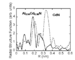
- FIG. 3 illustrates the radial structure function (RSF) of the gadolinium thin film and the Al 0.94 Gd 0.06 N crystal thin film in the X-ray absorption fine structure (XAFS) analysis.
- RSF radial structure function
- XAFS X-ray absorption fine structure
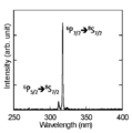
- the cathode ray emission spectrum of the produced Al 0.94 Gd 0.06 N at room temperature is shown in FIG.
- the acceleration voltage and the injection current are 3 kV and 0.5 mA, respectively.
- the line width of the cathode ray emission spectrum depends on the injection current. As shown in FIG. 4, the emission spectrum has a sharp peak at 317 nm.
- the emission spectrum also consists of two wavelengths of light (312 nm and 317 nm) emitted when returning from the lowest excited state 6 P 7/2 and the second excited state 6 P 5/2 to the ground state 8 S 7/2 . ing.
- the line width is about 1 nm, which is limited to the resolution of the monochromator.
- FIG. 5 shows the temperature dependence of the cathode ray emission intensity at room temperature of Al 0.94 Gd 0.06 N produced at a growth temperature of 100 ° C. to 500 ° C. From FIG. 5, it can be confirmed that the cathode ray emission intensity increases as the temperature decreases. As the growth temperature decreases, the thermal energy supplied from the substrate becomes insufficient during the growth process of the thin film crystal, and the diffusion of Gd atoms taken into the thin film is suppressed on the crystalline growth surface. As a result, Gd is uniformly distributed in the thin film. Is taken in. Thereby, it is considered that the average distance between Gd ions is increased and concentration quenching is suppressed. Further, AlN as a mother crystal is less likely to receive nitrogen having a high vapor pressure as the crystal growth temperature rises, and nitrogen defects are likely to occur. It is assumed that the growth at low temperature has succeeded in suppressing the generation of nitrogen defects.
- Example 2 describes an electronic excitation type light emitting device using the phosphor crystal thin film of the present invention.
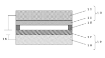
- FIG. 7 shows a configuration diagram of an electronic excitation light-emitting device of Example 2.
- the electron-excitation light-emitting device of Example 2 includes an anode electrode 13 obtained by growing the phosphor crystal thin film 11 produced in Example 1 described above on a quartz glass substrate 12, and a silicon substrate 18 with silicon.
- the gap between the anode electrode 13 and the cathode electrode 19 is used as a vacuum channel region, and by applying an electric field between the electrodes, electrons from the silicon-doped AlN thin film 17 that is an electron emission material are injected into the phosphor crystal thin film 11 to emit light.
- the phosphor crystal thin film 11 is formed with a thickness in the range of 100 nm to 100 ⁇ m.
- phosphor crystal thin films having a gadolinium content in AlN of 0.1 mol%, 1 mol%, 4 mol%, 6 mol%, and 11 mol% were prepared using a reactive RF magnetron sputtering apparatus.
- the substrate temperature during film formation was controlled at a low temperature of 200 ° C. to perform sputtering.
- an AlN buffer layer which is a pretreatment for growing an AlGdN crystal thin film, was not grown.
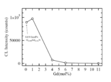
- FIG. 8 is a graph showing the Gd concentration dependency of cathode ray emission intensity (cathode luminescence intensity). From the graph of FIG. 8, it is understood that the cathode ray emission intensity is excellent when the Gd content is in the range of 0.1 to 6 mol%. In particular, when the Gd content is 0.1 to 1 mol%, the cathode ray emission intensity is remarkably excellent. Even when the Gd content is less than 0.1 mol%, for example, 0.01 mol%, high intensity cathode ray emission is expected as long as Gd exists as the emission center.
- FIG. 9 shows the Gd concentration dependence (1 mol%, 4 mol%, 6 mol%, 11 mol) of the radial structure function (RSF) of the Gd-L 3 absorption edge obtained by measurement for the Al 1-x Gd x N crystal thin film. %). From the graph of FIG. 9, it can be seen that the radial intensity of the radial structure function (RSF) increases as the Gd content decreases.
- XAFS X-ray absorption fine structure
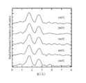
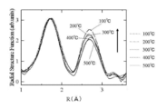
- FIG. 10 shows the film formation temperature dependence (100 ° C., 200 ° C.) of the radial structure function (RSF) of the Gd-L 3 absorption edge obtained by measurement of the Al 0.99 Gd 0.01 N crystal thin film. , 300 ° C., 400 ° C., 500 ° C.).
- FIG. 11 is a graph showing the film formation temperature dependence (100 ° C., 200 ° C., 300 ° C., 400 ° C., 500 ° C.) of the radial structure function (RSF) of a crystal thin film of Al 0.99 Gd 0.01 N. is there. From the graphs of FIGS. 10 and 11, it can be seen that the peak intensity of the second adjacent atom increases in the radial structure function (RSF) as the film formation temperature decreases.
- the radial structure function of the Gd-L 3 absorption edge obtained from the X-ray absorption fine structure (XAFS) measurement is based on the peak intensity of the first adjacent atom.
- the peak intensity of the second adjacent atom is high. This suggests that the coordination symmetry of the local structure of Gd is improved.
- FIG. 6 shows the temperature dependence of cathode ray emission intensity in a crystal thin film of Al 0.99 Gd 0.01 N.
- the horizontal axis in FIG. 6 indicates the substrate film forming temperature, and the vertical axis indicates the cathodoluminescence intensity.
- As the substrate film forming temperature six types of data of room temperature (25 ° C.), 100 ° C., 200 ° C., 300 ° C., 400 ° C., and 500 ° C. are measured. It can be confirmed from FIG. 6 that the cathode luminescence intensity of the crystalline thin film is remarkably lowered when the substrate film forming temperature is lowered to around room temperature (25 ° C.).
- FIG. 12 shows the second neighboring atoms of the radial structure function (RSF) of the crystalline thin film of the Gd 1 mol% sample (Al 0.99 Gd 0.01 N) and the Gd 6 mol% sample (Al 0.94 Gd 0.06 N). It is a graph which shows the correlation of the thickness of the buffer layer in the peak intensity of.
- RSF radial structure function
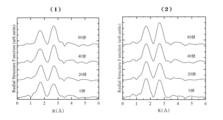
- FIG. 12 (1) shows a Gd 1 mol% sample, that is, a Gd concentration of 1 mol obtained by sputtering growth of a light emitting layer on a glass substrate at a substrate temperature of 200 ° C. for 60 minutes and a buffer layer for 0 minutes, 20 minutes, 40 minutes, and 80 minutes.
- % Gd-added AlN crystal thin film shows a Gd 6 mol% sample, that is, a Gd concentration obtained by sputtering growth on a glass substrate at a substrate temperature of 200 ° C. for 60 minutes, a buffer layer for 0 minutes, 20 minutes, 40 minutes, and 80 minutes. It is a 6 mol% Gd-added AlN crystal thin film.
- the film thicknesses of the buffer layers were 0, 20, 40, and 80 minutes, and the thicknesses of the respective buffer layers were 0 nm, 450 nm, 770 nm, and 1170 nm.
- 0 minutes, 20 minutes, 40 minutes, and 80 minutes indicate the film formation time of the buffer layer. From FIG. 12 (1), in the case of the radial structure function of the Gd-L 3 absorption edge of the Gd 1 mol% sample, it is observed that the peak intensity of the second adjacent atom increases as the thickness of the buffer layer increases. Is done. Also, from FIG.
- the radial structure function of the Gd-L 3 absorption edge of the Gd6 mol% sample is similar to that of the Gd 1 mol% sample, as the buffer layer thickness increases, A trend of increasing peak intensity is observed.
- An increase in the peak intensity of the second neighboring atom suggests that the coordination symmetry of Gd—Al or Gd—Gd is improved. This shows that the formation of the AlN buffer layer improves the coordination symmetry of the Gd local structure and increases the emission intensity of the light emitting layer.
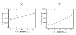
- FIG. 13 (1) shows a Gd 1 mol% sample, that is, a Gd concentration of 1 mol obtained by sputtering growth of a light-emitting layer on a glass substrate at a substrate temperature of 200 ° C. for 60 minutes, a buffer layer for 0 minutes, 20 minutes, 40 minutes, and 80 minutes. % Gd-added AlN crystal thin film.
- Gd 6 mol% sample that is, a Gd concentration obtained by sputtering growth on a glass substrate at a substrate temperature of 200 ° C. for 60 minutes and a buffer layer for 0 minutes, 20 minutes, 40 minutes, and 80 minutes. It is a 6 mol% Gd-added AlN crystal thin film.
- the film thicknesses of the buffer layers were 0 nm, 450 nm, 770 nm, and 1170 nm under the conditions of 0 minutes, 20 minutes, 40 minutes, and 80 minutes, respectively.
- FIG. 14 is a graph showing the Gd concentration dependence of the radial structure function (RSF) of a crystal thin film of Al 1-x Gd x N.
- RSF radial structure function
- FIG. 15 is a graph showing the correlation between the buffer layer deposition time (film thickness) of the crystal thin film of the Gd6 mol% sample (Al 0.94 Gd 0.06 N) and the X-ray diffraction measurement result.
- the buffer layer deposition time (film thickness) is 0 minutes, 5 minutes, 20 minutes, 40 minutes, and 80 minutes (0 nm, 140 nm, 450 nm, 770 nm, 1170 nm) for each of the X-ray diffraction patterns. The measurement results are shown. From FIG. 15, it can be confirmed that as the buffer layer deposition time (film thickness) increases, the X-ray diffraction peak appears sharply and the crystallinity is improved.
- the phosphor crystal thin film according to the present invention may be used for current industrial devices and analytical devices that are urgently being mercury-free.
- it can be expected to be used in a very wide range of application fields such as sterilization / sterilization equipment in the environment / medical field, cell sorting by dye, surface analysis, fluorescence analysis, environmental pollutant decomposition / removal equipment, water quality management system, etc.
Landscapes
- Chemical & Material Sciences (AREA)
- Engineering & Computer Science (AREA)
- Materials Engineering (AREA)
- Organic Chemistry (AREA)
- Metallurgy (AREA)
- Inorganic Chemistry (AREA)
- Crystallography & Structural Chemistry (AREA)
- Chemical Kinetics & Catalysis (AREA)
- Mechanical Engineering (AREA)
- Luminescent Compositions (AREA)
- Physical Vapour Deposition (AREA)
- Crystals, And After-Treatments Of Crystals (AREA)
Abstract
窒化アルミニウム中に高含有量の希土類金属イオンをドープさせた薄膜の結晶性をより高め、また濃度消光による発光強度の低下を回避して、高輝度な蛍光体結晶薄膜を提供する。具体的には、窒素雰囲気下でアルミニウムと希土類金属をスパッタリングする際に、窒化アルミニウム中の希土類金属の含有量が0.1~6mol%となるように金属ターゲットを用意し、基板温度を所定温度に低温制御してスパッタリングを行い、またスパッタリングに用いる真空槽内部の残留ガス中の水成分を除去して、希土類金属イオンドープの蛍光体結晶を成長させる。100℃以上300℃未満の温度範囲で蛍光体結晶薄膜を作製した結果、結晶薄膜の成長基板が低温なほど発光強度が高くなる。
Description
本発明は、窒化アルミニウム中に希土類金属イオンをドープさせた蛍光体結晶薄膜に関するもので、特に、窒化アルミニウム中に高含有量のガドリニウムイオンをドープさせて、高輝度な深紫外蛍光体結晶薄膜を提供する技術である。
最近、水銀ランプに変わる水銀フリー光源として窒化物半導体の発光ダイオードが積極的に研究されている。しかし、窒化ガリウムのバンドギャップで決まる365nmより短波長では高輝度発光は実現できていないのが実情である。これは、発光ダイオードは発光の活性層材料よりも大きなバンドギャップ材料でサンドイッチした構造を作らねばならないが、深紫外域で発光を得るためには最大のバンドギャップをもつ窒化アルミニウムでサンドイッチしてもキャリアの閉じ込めは不十分であり、発光効率は極端に落ちてしまうという要因から実現が困難となっている。
また、窒化アルミニウム結晶を半導体として用いた発光ダイオードで、波長210nmと短波長での紫外光の発光が報告されているが(非特許文献1)、発光出力や外部量子効率が小さく実用化が困難な状況である。
また、窒化アルミニウム結晶を半導体として用いた発光ダイオードで、波長210nmと短波長での紫外光の発光が報告されているが(非特許文献1)、発光出力や外部量子効率が小さく実用化が困難な状況である。
かかる状況下、本発明者は、実用化を目指した高輝度な深紫外光源デバイスを提供すべく、窒化アルミニウムをホスト材料として希土類金属イオンであるガドリニウム(Gd)を添加した紫外蛍光体結晶薄膜を有するアノード基板を備えた深紫外光源デバイスを提案している(特許文献1を参照)。高輝度な深紫外光源とするためには、窒化アルミニウム薄膜中に希土類金属イオンをドープさせた薄膜の結晶性をより高める必要がある。
また、窒化アルミニウム薄膜中に高含有量の希土類金属イオンをドープさせる方法も考えられる。しかしながら、発光中心となる希土類金属イオンが高含有率になると濃度消光によって発光強度が低下することが知られている。
かかる状況下、窒化アルミニウム中に高含有量のガドリニウムイオンをドープさせた薄膜の結晶性をより高め、また濃度消光による発光強度の低下を回避して、高輝度な深紫外光源の要素となる蛍光体結晶薄膜を得るべく、本発明者らは継続的に研究を行ってきた。
また、窒化アルミニウム薄膜中に高含有量の希土類金属イオンをドープさせる方法も考えられる。しかしながら、発光中心となる希土類金属イオンが高含有率になると濃度消光によって発光強度が低下することが知られている。
かかる状況下、窒化アルミニウム中に高含有量のガドリニウムイオンをドープさせた薄膜の結晶性をより高め、また濃度消光による発光強度の低下を回避して、高輝度な深紫外光源の要素となる蛍光体結晶薄膜を得るべく、本発明者らは継続的に研究を行ってきた。
波長210nmの紫外LED「絶縁体」のAlNで実現(日経エレクトロニクス(2006年6月19日号)P.30,31)、Nature 441, 325(2006).
上述したように、本発明は、窒化アルミニウム中に高含有量の希土類金属イオンをドープさせた薄膜の結晶性をより高め、また濃度消光による発光強度の低下を回避して、高輝度な蛍光体結晶薄膜を提供することを目的とする。
特に、3価の希土類金属イオンのGd3+イオンの内核電子遷移(4f軌道電子遷移)が効率よく約310nmのナローバンド紫外発光をすることの知見から、薄膜の結晶性をより高めて、濃度消光による発光強度の低下を回避し、窒化アルミニウム中に高含有量のガドリニウムイオンをドープさせて、高輝度な深紫外蛍光体結晶薄膜を提供する。
特に、3価の希土類金属イオンのGd3+イオンの内核電子遷移(4f軌道電子遷移)が効率よく約310nmのナローバンド紫外発光をすることの知見から、薄膜の結晶性をより高めて、濃度消光による発光強度の低下を回避し、窒化アルミニウム中に高含有量のガドリニウムイオンをドープさせて、高輝度な深紫外蛍光体結晶薄膜を提供する。
本発明者らは、継続的に研究を重ねる中で、蛍光体結晶薄膜の発光強度に関して、結晶薄膜の成膜時のドープされる希土類金属の濃度依存性,成膜基板の温度依存性,バッファー層の膜厚依存性があるという知見を得た。かかる知見は、結晶薄膜の成膜時のスパッタ温度が低温であればあるほど、蛍光体結晶薄膜の発光強度が増加するというものである。蛍光体結晶薄膜の発光強度は、結晶薄膜の結晶性,ドープされる発光中心の希土類金属イオンの含有量,バッファー層の厚さに左右されるのである。
本発明者らは、窒素雰囲気下でアルミニウムと希土類金属をスパッタリングする際に、基板温度を所定温度に低温制御してスパッタリングを行うことにより、結晶薄膜の結晶性の向上、濃度消光を抑制して高含有率の希土類金属イオンドープの蛍光体結晶を成長させることに成功したのである。また、バッファー層の膜厚を制御して薄膜結晶の高輝度化を図ったのである。
すなわち、前述の目的を達成するため、本発明の第1の観点の蛍光体結晶薄膜は、窒素雰囲気下でアルミニウムと希土類金属をスパッタリングすることにより作製された希土類金属イオンドープ窒化アルミニウム薄膜であって、窒化アルミニウム中の希土類金属の含有率が0.1~6mol%になるように金属ターゲットを用意し、基板温度を100℃以上300℃未満の範囲内に低温制御してスパッタリングを行うことにより、希土類金属の配位対称性を向上させて、高輝度の希土類金属イオンドープの蛍光体結晶薄膜を成膜するものである。
第1の観点の蛍光体結晶薄膜によれば、基板温度を低温制御することで、希土類金属の配位対称性を向上させて、高輝度の蛍光体結晶薄膜を作製することが可能となる。
ここで、基板温度を100℃以上300℃未満の範囲内に低温制御してスパッタリングを行う理由は以下の通りである。
300℃以上でスパッタリングを行うと、AlN結晶は良く成長するもののGdが凝集しやすく、濃度消光を起こしやすくなり、高輝度化とならないからである。また、100度未満でスパッタリングを行うと、結晶成長中の熱エネルギー不足で母体材料のAlN結晶(AlN結晶はウルツ鉱型構造を成す)そのものが形成されにくくなる。これらのトレードオフによって、希土類金属の配位対称性を向上させて高輝度の希土類金属イオンドープの蛍光体結晶薄膜を成膜する最適温度は、100℃以上300℃未満になる。
ここで、基板温度を100℃以上300℃未満の範囲内に低温制御してスパッタリングを行う理由は以下の通りである。
300℃以上でスパッタリングを行うと、AlN結晶は良く成長するもののGdが凝集しやすく、濃度消光を起こしやすくなり、高輝度化とならないからである。また、100度未満でスパッタリングを行うと、結晶成長中の熱エネルギー不足で母体材料のAlN結晶(AlN結晶はウルツ鉱型構造を成す)そのものが形成されにくくなる。これらのトレードオフによって、希土類金属の配位対称性を向上させて高輝度の希土類金属イオンドープの蛍光体結晶薄膜を成膜する最適温度は、100℃以上300℃未満になる。
後述する実施例で示すように、基板温度が100℃未満の室温付近で作製した試料のカソードルミネッセンス強度は低くなっているが、これはスパッタリングによるAlN結晶成長が不十分であることを示唆したものである。また、基板温度が300℃以上で作製した試料で、X線吸収微細構造(XAFS)測定より得られるGd-L3吸収端の動径構造関数は、第2近接原子のピーク強度が低くなっているが、これはGdの局所構造の配位対称性が低下したことを示唆したものである。
また、本発明の第2の観点の蛍光体結晶薄膜は、窒素雰囲気下でアルミニウムと希土類金属をスパッタリングすることにより作製された希土類金属イオンドープ窒化アルミニウム薄膜であって、窒化アルミニウム中の希土類金属の含有率が0.1~1mol%になるように金属ターゲットを用意し、基板温度を100~200℃の範囲内に低温制御してスパッタリングを行うことにより、希土類金属の配位対称性を向上させて、高輝度の希土類金属イオンドープの蛍光体結晶薄膜を成膜するものである。
第2の観点の蛍光体結晶薄膜によれば、より狭い範囲で、窒化アルミニウム中の希土類金属の含有率や基板温度を低温制御することで、希土類金属の配位対称性をより向上させて、より高輝度の蛍光体結晶薄膜を作製することが可能となる。
窒化アルミニウム中の希土類金属の含有率が0.1~1mol%になるようにし、かつ、基板温度を100~200℃の範囲内に低温制御してスパッタリングを行うことで、希土類金属の配位対称性をより向上させて、より高輝度の蛍光体結晶薄膜を作製できる。
窒化アルミニウム中の希土類金属の含有率が0.1~1mol%になるようにし、かつ、基板温度を100~200℃の範囲内に低温制御してスパッタリングを行うことで、希土類金属の配位対称性をより向上させて、より高輝度の蛍光体結晶薄膜を作製できる。
また、本発明の第3の観点の蛍光体結晶薄膜は、窒素雰囲気下でアルミニウムと希土類金属をスパッタリングすることにより作製された希土類金属イオンドープ窒化アルミニウム薄膜であって、窒化アルミニウム中の希土類金属の含有率が5mol%以上の高含有率となるように金属ターゲットを用意し、基板温度を100~200℃の範囲内に低温制御してスパッタリングを行うことにより、希土類金属の配位対称性を向上させて、濃度消光を抑制し、高輝度の希土類金属イオンドープの蛍光体結晶薄膜を成膜するものである。
第3の観点の蛍光体結晶薄膜によれば、希土類金属の配位対称性を向上させて、濃度消光を抑制し、高輝度の結晶薄膜を作製することが可能となる。
第3の観点の蛍光体結晶薄膜によれば、希土類金属の配位対称性を向上させて、濃度消光を抑制し、高輝度の結晶薄膜を作製することが可能となる。
次に、本発明の第4の観点の蛍光体結晶薄膜は、上記の第1の観点~第3の観点の蛍光体結晶薄膜において、基板上に生成させた所定の厚さ以上の窒化アルミニウムのバッファー層の上に、上述の低温制御のスパッタリングを行うことにより、所定の厚さ未満のバッファー層の上にスパッタリングを行い成膜した結晶薄膜よりも、希土類金属の配位対称性を向上させて、高輝度の希土類金属イオンドープの蛍光体結晶薄膜を成膜することが好ましい。
所定の厚さ以上のバッファー層上に、低温制御のスパッタリングを行うことにより、希土類金属の配位対称性をより向上することができ、より高輝度の結晶薄膜を作製することが可能となる。
所定の厚さ以上のバッファー層上に、低温制御のスパッタリングを行うことにより、希土類金属の配位対称性をより向上することができ、より高輝度の結晶薄膜を作製することが可能となる。
ここで、上記のバッファー層の所定の厚さは、具体的には、希土類金属としてガドリニウムを用いたX線吸収微細構造(XAFS)測定より得られるGd-L3吸収端の動径構造関数の第1近接原子のピーク強度より第2近接原子のピーク強度が大きくなる厚さである。バッファー層の所定の厚さを変化させたところ、吸収端の動径構造関数の第1近接原子のピーク強度の変化はみられないものの、吸収端の動径構造関数の第2近接原子のピーク強度がバッファー層の厚さに応じて増大するといった知見を得た。吸収端の動径構造関数の第1近接原子のピーク強度より第2近接原子のピーク強度が大きくなる厚さで、希土類金属の配位対称性が優れた、より高輝度の結晶薄膜が生成できるのである。
また、上記のバッファー層の所定の厚さは、具体的には、200~1400nmであることが好ましい態様である。従来、バッファー層は、希土類金属イオンドープ窒化アルミニウム薄膜をガラス基板上に安定的に成長させるために用いられており、バッファー層を設けた方が結晶薄膜の結晶性を向上できることは知られていたが、この場合のバッファー層は存在すればよいとの認識で、0~200nm程度の厚さであった。
今回、実験を重ねた結果、バッファー層の厚さを、200~1400nmにすることにより、希土類金属の配位対称性が優れた、より高輝度の結晶薄膜が生成できることの知見を得たものである。ここで、バッファー層の厚さは厚い方がより高輝度の結晶薄膜が生成できている。但し、バッファー層自体、あまりに厚くすると結晶薄膜の発光中心からの発光を阻害する要因となるため、厚さの上限(ここでは1400nm)を設けたものである。
次に、上記の第1の観点~第4の観点の蛍光体結晶薄膜において、基板温度を所定温度で低温制御してスパッタリングを行うと共に、スパッタリングに用いる真空槽内部の残留ガス中の水成分を所定圧力以下に除去することがより好ましい。
スパッタリングに用いる真空槽内部の残留ガス中の水成分を所定圧力以下に除去しながら行うことにより、蛍光体結晶薄膜の結晶性を向上することができ、発光のピーク強度がより大きく、高輝度な蛍光体結晶薄膜を得ることが可能となる。また、かかる条件で、安価で高品質な大面積の蛍光体結晶薄膜の作製が可能となる。
スパッタリングに用いる真空槽内部の残留ガス中の水成分を所定圧力以下に除去しながら行うことにより、蛍光体結晶薄膜の結晶性を向上することができ、発光のピーク強度がより大きく、高輝度な蛍光体結晶薄膜を得ることが可能となる。また、かかる条件で、安価で高品質な大面積の蛍光体結晶薄膜の作製が可能となる。
ここで、スパッタリングに用いる真空槽内部の残留ガス中の水成分は、好ましくは、10-5Pa以下となる条件とする。かかる真空槽内部の残留ガス中の水成分除去のための具体的な方法としては、スパッタリング装置に液体窒素トラップ若しくはクライオポンプを配設することである。ここで、液体窒素トラップは、例えば、コールドフィンガーを用いて、スパッタリング装置の排気回路部に設けるか、ターゲット基板の近傍に設けるものである。
また、上記の蛍光体結晶薄膜に添加される希土類金属イオンとしては、ガドリニウム(Gd)、ユウロピウム(Eu)、ジプシロシウム(Dy)、ランタン(La)、セリウム(Ce)、サマリウム(Sm)、イットリウム(Y)、ネオジウム(Nd)、テルビウム(Tb)、プラセオジム(Pr)、エルビウム(Er)、ツリウム(Tm)、イッテルビウム(Yb)、スカンジウム(Sc)、プロメチウム(Pm)、ホルミウム(Ho)、およびルテチウム(Lu)等のイオンが例示される。希土類元素のイオンは、4f禁制遷移による発光、又は4f-5d許容遷移による発光を示す。4f禁制遷移による発光中心元素としては、Gd3+(深紫外色),Tm3+(青色),Tb3+(緑色),Sm3+(赤色)等がある。許容遷移による発光中心元素としては、Ce3+,Eu2+等がある。
希土類金属イオンは、特に限定されるものではないが、紫外領域の発光中心となるガドリニウム(Gd)又はGd化合物が選ばれることが好ましい。ガドリニウム(Gd)を発光中心とすることで、滅菌・殺菌能力に優れた近紫外光源デバイスを得ることが可能となる。すなわち、Gd3+イオンの発光ピーク波長は約315nm付近であり、毒性の強いテトラクロロダイオキシン類の光分解、DNA分解を利用した殺菌応用や,光触媒応用などに極めて有望な元素である。
次に、本発明の蛍光体結晶薄膜の作製方法は、窒素雰囲気下でアルミニウムと希土類金属をスパッタリングする希土類金属イオンドープ窒化アルミニウム薄膜の作製方法であって、
1-1)スパッタリングに用いる真空槽内部の残留ガス中の水成分を10-5Pa以下に除去する工程と、
1-2)基板上に所定の厚さの窒化アルミニウムのバッファー層を生成するバッファー層生成工程と、
1-3)窒化アルミニウム中の希土類金属の含有率が0.1~6mol%の含有率となるように金属ターゲットを用意し、基板温度を100℃以上300℃未満の範囲内に低温制御するスパッタリング工程と、
を備え、希土類金属の配位対称性を向上させて、高輝度の希土類金属イオンドープの蛍光体結晶薄膜を前記バッファー層上に成膜することを特徴とする方法である。
かかる方法によれば、従来方法に比べて、高含有率の希土類金属イオンドープの結晶薄膜を作製することが可能で、高輝度の蛍光体結晶薄膜を得ることができる。
1-1)スパッタリングに用いる真空槽内部の残留ガス中の水成分を10-5Pa以下に除去する工程と、
1-2)基板上に所定の厚さの窒化アルミニウムのバッファー層を生成するバッファー層生成工程と、
1-3)窒化アルミニウム中の希土類金属の含有率が0.1~6mol%の含有率となるように金属ターゲットを用意し、基板温度を100℃以上300℃未満の範囲内に低温制御するスパッタリング工程と、
を備え、希土類金属の配位対称性を向上させて、高輝度の希土類金属イオンドープの蛍光体結晶薄膜を前記バッファー層上に成膜することを特徴とする方法である。
かかる方法によれば、従来方法に比べて、高含有率の希土類金属イオンドープの結晶薄膜を作製することが可能で、高輝度の蛍光体結晶薄膜を得ることができる。
次に、本発明の電子励起型発光デバイスは、アノード電極と、熱フィラメントや冷陰極材料など電子放出材料からなるカソード電極と、アノード電極とカソード電極とを対向して配設させ、基板間の空隙を高真空雰囲気に保持させるスペーサと、アノード電極とカソード電極の間に電界を印加させる電圧回路とを少なくとも有し、アノード電極とカソード電極の間の空隙を真空チャネル領域として、電極間に電界を印加することにより電子放出材料からの電子を蛍光体結晶薄膜に注入させて発光させる構成とされ、アノード電極が第1の観点~第4の観点のいずれかの蛍光体結晶薄膜から成り、蛍光体結晶薄膜が100nm~100μmの膜厚で形成されることを特徴とするものである。
カソード電極を構成する熱フィラメントや冷陰極材料などの電子放出材料に電圧が印加されると、電界放出により電子が発生し真空中に放たれる。この電子がアノード電極に引き寄せられて進み、アノード電極を構成する本発明の蛍光体結晶薄膜に衝突する。電子が衝突することにより蛍光体結晶薄膜は電子エネルギーを光エネルギーに変換して発光することとなる。かかる蛍光体結晶薄膜の膜厚を100nm~100μmに形成させることで、高輝度な電子励起型発光デバイスを得ることができる。
ここで、アノード電極は本発明の蛍光体結晶薄膜から成るもので、ガラス基板上に窒化アルミニウム(AlN)バッファー層を堆積させ、その上に希土類金属イオンドープ窒化アルミニウム薄膜を成長させたものである。さらに成長させた膜表面上に酸化防止用の保護膜を形成してもよい。かかる構成のアノード電極を用いることにより、高輝度の電子励起型発光デバイスを得ることができる。
本発明よれば、窒化アルミニウム中に高含有量の希土類金属イオンをドープさせた薄膜の結晶性をより高め、また濃度消光による発光強度の低下を回避して、高輝度な蛍光体結晶薄膜を作製できる。
以下、本発明の実施形態の一例を、図面を参照しながら詳細に説明していく。
(蛍光体結晶薄膜の作製装置について)
先ず、蛍光体結晶薄膜の作製装置について説明する。図1は、蛍光体結晶薄膜の作製に用いる反応性RFマグネトロンスパッタリング装置の構造模式図である。
以下、図1のスパッタリング装置を参照して、蛍光体結晶薄膜の作製方法について説明する。蛍光体結晶薄膜の作製に用いた反応性RFマグネトロンスパッタリング装置30は、装置内の真空チャンバー上部にヒータ32を有し、真空チャンバー下部に高周波電源32(図示しない)を有する。真空チャンバー右部には、反応ガス33を導入できる流入口がある。真空チャンバー左部の流出口には、液体窒素トラップ20が備えられ、スパッタリング装置内の真空チャンバー内部の残留ガス中の水成分を積極的に除去している。そして、真空ポンプ39(図示しない)によって反応ガスを流出させる。
先ず、蛍光体結晶薄膜の作製装置について説明する。図1は、蛍光体結晶薄膜の作製に用いる反応性RFマグネトロンスパッタリング装置の構造模式図である。
以下、図1のスパッタリング装置を参照して、蛍光体結晶薄膜の作製方法について説明する。蛍光体結晶薄膜の作製に用いた反応性RFマグネトロンスパッタリング装置30は、装置内の真空チャンバー上部にヒータ32を有し、真空チャンバー下部に高周波電源32(図示しない)を有する。真空チャンバー右部には、反応ガス33を導入できる流入口がある。真空チャンバー左部の流出口には、液体窒素トラップ20が備えられ、スパッタリング装置内の真空チャンバー内部の残留ガス中の水成分を積極的に除去している。そして、真空ポンプ39(図示しない)によって反応ガスを流出させる。
反応ガス33は真空ポンプ39(図示しない)によって、入った方向の対角の方向に出て行くように設計されており、スパッタが起こるチャンバー中央部に供給されるようになっている。また、マグネット40近傍には水冷管41が設けられており、スパッタによりターゲットが加熱され、溶解することを防止している。チャンバー本体にも水冷管42を設けており、プラズマによるチャンバーの温度上昇によるプラズマ状態の変化を防いでいる。
また、ターゲット36と基板34の間にシャッターを配設して、シャッターの開閉により、得られる結晶薄膜の膜厚を制御している。
また、ターゲット36と基板34の間にシャッターを配設して、シャッターの開閉により、得られる結晶薄膜の膜厚を制御している。
実施例1では、窒化アルミニウム中に高含有量のガドリニウムイオンをドープさせ、100℃~500℃の温度範囲で蛍光体結晶薄膜を作製したものの発光特性を示す。
先ず、蛍光体結晶薄膜の作製方法について説明する。上述の反応性RFマグネトロンスパッタリング装置30の上部に、基板として深紫外域で透明な石英ガラス基板34を収め、石英ガラス基板34と対向して下部にAl/Gdターゲット35を載置する。Al/Gdターゲット35は、図1の右下に示すように、Alターゲット36の上に1.5mm角のGd金属チップ37を所定個数載置する。ターゲットはAlとGdの組成を制御した合金ターゲットでも良い。Gd濃度はチップの数やチップ面積を変えることで制御する。
先ず、蛍光体結晶薄膜の作製方法について説明する。上述の反応性RFマグネトロンスパッタリング装置30の上部に、基板として深紫外域で透明な石英ガラス基板34を収め、石英ガラス基板34と対向して下部にAl/Gdターゲット35を載置する。Al/Gdターゲット35は、図1の右下に示すように、Alターゲット36の上に1.5mm角のGd金属チップ37を所定個数載置する。ターゲットはAlとGdの組成を制御した合金ターゲットでも良い。Gd濃度はチップの数やチップ面積を変えることで制御する。
次に、ヒータ31を制御して、石英ガラス基板34の温度を100℃~500℃の温度範囲で制御した。チャンバー内にN2とArガスの反応ガス33を流して、スパッタ電圧1.8kV,RFパワー150Wでスパッタリングを行った。チャンバーの背圧は約6×10⁻⁶Pa未満である。また、反応ガス22の全圧は、5Paで分圧比は1対1である。
そして、スパッタリングを行うことで、石英ガラス基板34上にガドリニウムが添加されたAlGdNの結晶薄膜を成長させた。AlN中のガドリニウムの含有率が6mol%となるように金属ターゲットを用意した。成長温度は100℃~500℃の範囲で変更した。
そして、スパッタリングを行うことで、石英ガラス基板34上にガドリニウムが添加されたAlGdNの結晶薄膜を成長させた。AlN中のガドリニウムの含有率が6mol%となるように金属ターゲットを用意した。成長温度は100℃~500℃の範囲で変更した。
また、AlGdNの結晶薄膜を成長させる前処理として、石英ガラス基板34上にAlNバッファー層を100nm成長させた。そして、AlN中のガドリニウムの含有率が6mol%となるAl0.94Gd0.06Nの結晶薄膜を270nm積層させた。
図2は、石英ガラス基板上に形成させたAlGdNの結晶薄膜のX線回折スペクトル(XRD)を示している。図2に示されるように、X線回折スペクトルは、成長温度100℃~500℃のすべてにおいて、(002)配向した結晶特性を有しており、高品質の結晶膜を作製できたことになる。
次に、図3は、X線吸収微細構造(XAFS)解析でのガドリニウム薄膜とAl0.94Gd0.06N 結晶薄膜の動径構造関数(RSF)を図示したものである。図3に示されるように、Al0.94Gd0.06Nの構造関数は、GdNの構造関数と異なっており、GdNの0.3nm付近での特性ピークは、Al0.94Gd0.06Nで見られない。従って、GdNクラスターはAl0.94Gd0.06Nで形成されていないことが判る。このことは、ガドリニウム(Gd)原子は、アルミニウム(Al)原子の位置を正確に占有しているといえる。
次に、作製したAl0.94Gd0.06Nの室温での陰極線発光スペクトルを図4に示す。
加速電圧と注入電流はそれぞれ3kVと0.5mAである。陰極線発光スペクトルの線幅は注入電流に依存する。図4に示すように、発光スペクトルは317nmに鋭いピークを持つ。また発光スペクトルは、最低励起状態6P7/2と第二励起状態6P5/2から基底状態8S7/2へ戻るときに放出された2つの波長の光(312nmと317nm)から成り立っている。線幅は約1nmであり、単色光分光器の分解能に制限されている。
加速電圧と注入電流はそれぞれ3kVと0.5mAである。陰極線発光スペクトルの線幅は注入電流に依存する。図4に示すように、発光スペクトルは317nmに鋭いピークを持つ。また発光スペクトルは、最低励起状態6P7/2と第二励起状態6P5/2から基底状態8S7/2へ戻るときに放出された2つの波長の光(312nmと317nm)から成り立っている。線幅は約1nmであり、単色光分光器の分解能に制限されている。
成長温度100℃~500℃で作製したAl0.94Gd0.06Nの室温での陰極線発光強度の温度依存性を図5に示す。図5から、陰極線発光強度は温度低下とともに増加することが確認できる。成長温度が下がるに従って、薄膜結晶の成長過程で基板から供給される熱エネルギーが十分でなくなり、結晶性成長面では薄膜に取り込まれるGd原子の拡散が抑制され、その結果、Gdが均質に薄膜中に取り込まれる。これにより、Gdイオン間の平均距離が増加し、濃度消光が抑制されていると考えられる。さらに母結晶のAlNは結晶成長温度上昇とともに蒸気圧の高い窒素が取り込まれにくくなり、窒素欠陥を生じやすくなる。低温における成長ではこの窒素欠陥の生成を抑えることにも成功していると推察する。
実施例2は、本発明の蛍光体結晶薄膜を用いた電子励起型発光デバイスについて説明する。図7は、実施例2の電子励起型発光デバイスの構成図を示している。図7に示すように、実施例2の電子励起型発光デバイスは、上述した実施例1で作製した蛍光体結晶薄膜11を石英ガラス基板12に成長させたアノード電極13と、シリコン基板18にシリコンドープAlN薄膜17を成長させたカソード電極19と、アノード電極13とカソード電極19とを対向して配設させ、基板間の空隙を高真空雰囲気に保持させるスペーサ15と、アノード電極13とカソード電極19の間に電界を印加させる電圧回路16とから構成されるものである。
アノード電極13とカソード電極19の間の空隙を真空チャネル領域として、電極間に電界を印加することにより電子放出材料であるシリコンドープAlN薄膜17からの電子を蛍光体結晶薄膜11に注入させて発光させる。この蛍光体結晶薄膜11の膜厚は、100nm~100μmの範囲で形成される。
(陰極線発光強度のGd濃度依存性について)
実施例1と同様に、反応性RFマグネトロンスパッタリング装置を用いて、AlN中のガドリニウムの含有率が、0.1mol%,1mol%,4mol%,6mol%,11mol%の蛍光体結晶薄膜を作製した。ここで、成膜時の基板温度は200℃に低温制御してスパッタリングを実施した。なお、実施例1と異なり、AlGdNの結晶薄膜を成長させる前処理となるAlNバッファー層は成長させなかった。
実施例1と同様に、反応性RFマグネトロンスパッタリング装置を用いて、AlN中のガドリニウムの含有率が、0.1mol%,1mol%,4mol%,6mol%,11mol%の蛍光体結晶薄膜を作製した。ここで、成膜時の基板温度は200℃に低温制御してスパッタリングを実施した。なお、実施例1と異なり、AlGdNの結晶薄膜を成長させる前処理となるAlNバッファー層は成長させなかった。
図8は、陰極線発光強度(カソードルミネッセンス強度)のGd濃度依存性を示すグラフである。図8のグラフから、0.1~6mol%の範囲のGd含有率の場合、陰極線発光強度が優れたものとなっていることがわかる。特に、0.1~1mol%のGd含有率の場合、陰極線発光強度が顕著に優れたものとなっている。なお、0.1mol%未満、例えば、0.01mol%のGd含有率の場合であっても、発光中心としてGdが存在する限りにおいては高い強度の陰極線発光が観測されることが予想される。
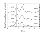
図9は、Al1-xGdxNの結晶薄膜について測定より得られたGd-L3吸収端の動径構造関数(RSF)のGd濃度依存性(1mol%,4mol%,6mol%,11mol%)を示すグラフである。図9のグラフから、動径構造関数(RSF)は、Gdの含有量が少なくなるにつれて、第2近接原子(図中の矢印の部分)のピーク強度が増大していることがわかる。ここで、X線吸収微細構造(XAFS)解析の結果から、動径構造関数(RSF)の第2近接原子のピーク強度と発光強度が大きく関係していることが知られている。
また、図10は、Al0.99Gd0.01Nの結晶薄膜について測定より得られたGd-L3吸収端の動径構造関数(RSF)の成膜温度依存性(100℃,200℃,300℃,400℃,500℃)を示すグラフである。図11は、Al0.99Gd0.01Nの結晶薄膜の動径構造関数(RSF)の成膜温度依存性(100℃,200℃,300℃,400℃,500℃)を示すグラフである。図10と図11のグラフから、動径構造関数(RSF)は、成膜温度が低くなるにつれて、第2近接原子のピーク強度が増大していることがわかる。
また、成膜温度が100℃,200℃で作製した試料は、X線吸収微細構造(XAFS)測定より得られるGd-L3吸収端の動径構造関数は、第1近接原子のピーク強度より第2近接原子のピーク強度が高くなっている。これはGdの局所構造の配位対称性が向上したことを示唆している。
図6は、Al0.99Gd0.01Nの結晶薄膜における陰極線発光強度の温度依存性を示している。図6の横軸は基板成膜温度を示しており、縦軸はカソードルミネッセンス強度を示している。基板成膜温度は、室温(25℃)、100℃,200℃,300℃,400℃,500℃の6種類のデータを測定している。図6から室温(25℃)付近まで基板成膜温度が低下すると結晶薄膜のカソードルミネッセンス強度が著しく低下していることが確認できる。これは、基板温度が室温(25℃)付近まで低下することで、スパッタリングにより膜成長するために必要な熱エネルギーが不足し、AlN結晶成長が不十分となることに起因するものである。このことから、低温制御してスパッタリングを行う場合でも、室温(25℃)以上の温度が必要となるのである。
(バッファー層の厚さと結晶薄膜の発光強度との相関性について)
実施例4では、バッファー層の厚さと結晶薄膜の発光強度との相関性について説明する。
先ず図12は、Gd1mol%試料(Al0.99Gd0.01N)とGd6mol%試料(Al0.94Gd0.06N)の結晶薄膜の動径構造関数(RSF)の第2近接原子のピーク強度におけるバッファー層の厚さの相関を示すグラフである。図12(1)は、Gd1mol%試料、すなわち、ガラス基板上に200℃の基板温度で発光層を60分、バッファー層を0分,20分,40分,80分スパッタ成長したGd濃度1モル%のGd添加AlN結晶薄膜である。また、図12(2)は、Gd6mol%試料、すなわち、ガラス基板上に200℃の基板温度で発光層を60分、バッファー層を0分,20分,40分,80分スパッタ成長したGd濃度6モル%のGd添加AlN結晶薄膜である。
実施例4では、バッファー層の厚さと結晶薄膜の発光強度との相関性について説明する。
先ず図12は、Gd1mol%試料(Al0.99Gd0.01N)とGd6mol%試料(Al0.94Gd0.06N)の結晶薄膜の動径構造関数(RSF)の第2近接原子のピーク強度におけるバッファー層の厚さの相関を示すグラフである。図12(1)は、Gd1mol%試料、すなわち、ガラス基板上に200℃の基板温度で発光層を60分、バッファー層を0分,20分,40分,80分スパッタ成長したGd濃度1モル%のGd添加AlN結晶薄膜である。また、図12(2)は、Gd6mol%試料、すなわち、ガラス基板上に200℃の基板温度で発光層を60分、バッファー層を0分,20分,40分,80分スパッタ成長したGd濃度6モル%のGd添加AlN結晶薄膜である。
ここで、バッファー層は、その成膜時間が0分,20分,40分,80分の条件で、各々のバッファー層の膜厚は0nm,450nm,770nm,1170nmであった。図12のグラフ中、0分,20分,40分,80分は、バッファー層の成膜時間を示している。
図12(1)から、Gd1mol%試料のGd-L3吸収端の動径構造関数の場合、バッファー層の膜厚が増加するに従い、第2近接原子のピーク強度が増加していく傾向が観察される。また、図12(2)から、Gd6mol%試料のGd-L3吸収端の動径構造関数も、Gd1mol%試料の場合と同様に、バッファー層の膜厚が増加するに従い、第2近接原子のピーク強度が増加していく傾向が観察される。
第2近接原子のピーク強度が増加することは、Gd-Al又はGd-Gdの配位対称性が向上していることを示唆している。このことから、AlNのバッファー層の形成により、Gd局所構造の配位対称性が向上し、発光層の発光強度の増大化が図れることがわかる。
図12(1)から、Gd1mol%試料のGd-L3吸収端の動径構造関数の場合、バッファー層の膜厚が増加するに従い、第2近接原子のピーク強度が増加していく傾向が観察される。また、図12(2)から、Gd6mol%試料のGd-L3吸収端の動径構造関数も、Gd1mol%試料の場合と同様に、バッファー層の膜厚が増加するに従い、第2近接原子のピーク強度が増加していく傾向が観察される。
第2近接原子のピーク強度が増加することは、Gd-Al又はGd-Gdの配位対称性が向上していることを示唆している。このことから、AlNのバッファー層の形成により、Gd局所構造の配位対称性が向上し、発光層の発光強度の増大化が図れることがわかる。
図12(1)と図12(2)のGd-L3吸収端の動径構造関数を比較すると、低濃度である1mol%の方が第2近接原子のピーク強度が大きいことが確認できる。これらの試料のカソードルミネッセンス強度を比較すると、Gd濃度1mol%の方がGd濃度6mol%に比べて発光強度が大きい結果となっていた。
次に、図13のグラフでは、Gd1mol%試料(Al0.99Gd0.01N)とGd6mol%試料(Al0.94Gd0.06N)の結晶薄膜のバッファー層成膜時間と陰極線発光強度との相関を示している。
図13(1)は、Gd1mol%試料、すなわち、ガラス基板上に200℃の基板温度で発光層を60分、バッファー層を0分,20分,40分,80分スパッタ成長したGd濃度1モル%のGd添加AlN結晶薄膜である。また、図13(2)は、Gd6mol%試料、すなわち、ガラス基板上に200℃の基板温度で発光層を60分、バッファー層を0分,20分,40分,80分スパッタ成長したGd濃度6モル%のGd添加AlN結晶薄膜である。上述したように、バッファー層は、その成膜時間が0分,20分,40分,80分の条件で、各々のバッファー層の膜厚は0nm,450nm,770nm,1170nmであった。
図13(1)は、Gd1mol%試料、すなわち、ガラス基板上に200℃の基板温度で発光層を60分、バッファー層を0分,20分,40分,80分スパッタ成長したGd濃度1モル%のGd添加AlN結晶薄膜である。また、図13(2)は、Gd6mol%試料、すなわち、ガラス基板上に200℃の基板温度で発光層を60分、バッファー層を0分,20分,40分,80分スパッタ成長したGd濃度6モル%のGd添加AlN結晶薄膜である。上述したように、バッファー層は、その成膜時間が0分,20分,40分,80分の条件で、各々のバッファー層の膜厚は0nm,450nm,770nm,1170nmであった。
図13のグラフから、Gd1mol%試料とGd6mol%試料のいずれの場合も、バッファー層の成膜時間が長くなるほど、すなわち、バッファー層の膜厚が厚くなるほど、カソードルミネッセンス強度が大きくなる傾向が確認できる。図13(1)(2)のグラフ中の右上がりの線は、傾向を見やすくするための参考線である。
図14は、Al1-xGdxNの結晶薄膜の動径構造関数(RSF)のGd濃度依存性を示すグラフである。Gd含有率が1mol%,4mol%,6mol%の場合の動径構造関数(RSF)を観察すると、Gd含有率が大きくなるほど、動径構造関数(RSF)の 第1近接原子の1.7オングストローム付近のピークが長距離側にシフトしていくことが確認できる。これは、Gd-N結合距離が伸びていることを示している。
図15は、Gd6mol%試料(Al0.94Gd0.06N)の結晶薄膜のバッファー層成膜時間(膜厚)とX線回折測定結果の相関を示すグラフである。バッファー層成膜時間(膜厚)は、0分,5分、20分,40分,80分(0nm,140nm,450nm,770nm,1170nm)の5種類の試料に対して、それぞれのX線回折測定結果を示している。
図15から、バッファー層成膜時間(膜厚)が大きくなるほど、X線回折ピークが鋭く現れており、結晶性が向上していることが確認できる。
図15から、バッファー層成膜時間(膜厚)が大きくなるほど、X線回折ピークが鋭く現れており、結晶性が向上していることが確認できる。
本発明に係る蛍光体結晶薄膜は、水銀レス化が急がれる現在の工業用装置や分析装置類への利用可能性がある。また、環境・医療現場における殺菌・滅菌装置,色素による細胞選別、表面分析、蛍光分析や、環境汚染物質の分解・除去装置、水質管理システム等の極めて広範囲の応用分野広範囲な利用が期待できる。
20 液体窒素トラップ
30 反応性RFマグネトロンスパッタリング装置
31 ヒータ
32 高周波電源
33 反応ガス(N2とArガス)
34 石英ガラス基板
35 Al/Gdターゲット
36 Alターゲット
37 Gdチップ
38 マッチングボックス
39 真空ポンプ
40 マグネット
41 水冷管(マグネット近傍)
42 水冷管(チャンバー本体)
30 反応性RFマグネトロンスパッタリング装置
31 ヒータ
32 高周波電源
33 反応ガス(N2とArガス)
34 石英ガラス基板
35 Al/Gdターゲット
36 Alターゲット
37 Gdチップ
38 マッチングボックス
39 真空ポンプ
40 マグネット
41 水冷管(マグネット近傍)
42 水冷管(チャンバー本体)
Claims (12)
- 窒素雰囲気下でアルミニウムと希土類金属をスパッタリングすることにより作製された希土類金属イオンドープ窒化アルミニウム薄膜であって、
窒化アルミニウム中の希土類金属の含有率が0.1~6mol%となるように金属ターゲットを用意し、基板温度を100℃以上300℃未満の範囲内に低温制御してスパッタリングを行うことにより、希土類金属の配位対称性を向上させて、高輝度の希土類金属イオンドープの蛍光体結晶薄膜を成膜することを特徴とする蛍光体結晶薄膜。 - 窒素雰囲気下でアルミニウムと希土類金属をスパッタリングすることにより作製された希土類金属イオンドープ窒化アルミニウム薄膜であって、
窒化アルミニウム中の希土類金属の含有率が0.1~1mol%となるように金属ターゲットを用意し、基板温度を100~200℃の範囲内に低温制御してスパッタリングを行うことにより、希土類金属の配位対称性を向上させて、高輝度の希土類金属イオンドープの蛍光体結晶薄膜を成膜することを特徴とする蛍光体結晶薄膜。 - 窒素雰囲気下でアルミニウムと希土類金属をスパッタリングすることにより作製された希土類金属イオンドープ窒化アルミニウム薄膜であって、
窒化アルミニウム中の希土類金属の含有率が5mol%以上の高含有率となるように金属ターゲットを用意し、基板温度を100~200℃の範囲内に低温制御してスパッタリングを行うことにより、希土類金属の配位対称性を向上させて、濃度消光を抑制し、高輝度の希土類金属イオンドープの蛍光体結晶薄膜を成膜することを特徴とする蛍光体結晶薄膜。 - 請求項1~3のいずれかの蛍光体結晶薄膜において、基板上に生成させた所定の厚さ以上の窒化アルミニウムのバッファー層の上に前記スパッタリングを行うことにより、所定の厚さ未満の前記バッファー層の上に前記スパッタリングを行い成膜した結晶薄膜よりも、希土類金属の配位対称性を向上させて、高輝度の希土類金属イオンドープの蛍光体結晶薄膜を成膜することを特徴とする蛍光体結晶薄膜。
- 前記バッファー層の所定の厚さは、希土類金属としてガドリニウムを用いたX線吸収微細構造(XAFS)測定より得られるGd-L3吸収端の動径構造関数の第1近接原子のピーク強度より第2近接原子のピーク強度が大きくなる厚さであることを特徴とする請求項4に記載の蛍光体結晶薄膜。
- 前記バッファー層の所定の厚さは、200~1400nmであることを特徴とする請求項4に記載の蛍光体結晶薄膜。
- 請求項1~4のいずれかの蛍光体結晶薄膜において、基板温度を所定温度で低温制御してスパッタリングを行うと共に、スパッタリングに用いる真空槽内部の残留ガス中の水成分を所定圧力以下に除去することを特徴とする蛍光体結晶薄膜。
- 請求項1~4のいずれかの蛍光体結晶薄膜において、基板温度を所定温度で低温制御してスパッタリングを行うと共に、スパッタリングに用いる真空槽内部の残留ガス中の水成分を10-5Pa以下に除去することを特徴とする蛍光体結晶薄膜。
- 前記希土類金属が、Gd、Eu、Dy、La、Ce、Sm、Y、Nd、Tb、Pr、Er、Tm、Yb、Sc、Pm、Ho、およびLuからなる群より選択される、少なくとも1種の金属であることを特徴とする請求項1~4のいずれかの蛍光体結晶薄膜。
- 前記蛍光体結晶薄膜の発光中心としてGd又はGd化合物が選ばれることを特徴とする請求項1~4のいずれかの蛍光体結晶薄膜。
- 窒素雰囲気下でアルミニウムと希土類金属をスパッタリングする希土類金属イオンドープ窒化アルミニウム薄膜の作製方法であって、
スパッタリングに用いる真空槽内部の残留ガス中の水成分を10-5Pa以下に除去する工程と、
基板上に所定の厚さの窒化アルミニウムのバッファー層を生成するバッファー層生成工程と、
窒化アルミニウム中の希土類金属の含有率が0.1~6mol%の含有率となるように金属ターゲットを用意し、基板温度を100℃以上300℃未満の範囲内に低温制御するスパッタリング工程と、
を備え、希土類金属の配位対称性を向上させて、高輝度の希土類金属イオンドープの蛍光体結晶薄膜を前記バッファー層上に成膜することを特徴とする蛍光体結晶薄膜の作製方法。 - アノード電極と、熱フィラメントや冷陰極材料など電子放出材料からなるカソード電極と、前記アノード電極と前記カソード電極とを対向して配設させ、基板間の空隙を高真空雰囲気に保持させるスペーサと、前記アノード電極と前記カソード電極の間に電界を印加させる電圧回路とを少なくとも有し、前記アノード電極と前記カソード電極の間の空隙を真空チャネル領域として、電極間に電界を印加することにより前記電子放出材料からの電子を前記蛍光体結晶薄膜に注入させて発光させる構成の電子励起型発光デバイスにおいて、
前記アノード電極が請求項1~4のいずれかの蛍光体結晶薄膜から成り、
前記蛍光体結晶薄膜が、100nm~100μmの膜厚で形成されていることを特徴とする電子励起型発光デバイス。
Priority Applications (1)
| Application Number | Priority Date | Filing Date | Title |
|---|---|---|---|
| JP2011521822A JP5476531B2 (ja) | 2009-07-07 | 2010-07-07 | 蛍光体結晶薄膜とその作製方法 |
Applications Claiming Priority (2)
| Application Number | Priority Date | Filing Date | Title |
|---|---|---|---|
| JP2009-161277 | 2009-07-07 | ||
| JP2009161277 | 2009-07-07 |
Publications (1)
| Publication Number | Publication Date |
|---|---|
| WO2011004601A1 true WO2011004601A1 (ja) | 2011-01-13 |
Family
ID=43429029
Family Applications (1)
| Application Number | Title | Priority Date | Filing Date |
|---|---|---|---|
| PCT/JP2010/004445 Ceased WO2011004601A1 (ja) | 2009-07-07 | 2010-07-07 | 蛍光体結晶薄膜とその作製方法 |
Country Status (2)
| Country | Link |
|---|---|
| JP (1) | JP5476531B2 (ja) |
| WO (1) | WO2011004601A1 (ja) |
Cited By (9)
| Publication number | Priority date | Publication date | Assignee | Title |
|---|---|---|---|---|
| CN102719243A (zh) * | 2012-06-01 | 2012-10-10 | 华南农业大学 | 一种锰离子激活红色长余辉发光材料及其制备方法 |
| US9136819B2 (en) | 2012-10-27 | 2015-09-15 | Avago Technologies General Ip (Singapore) Pte. Ltd. | Bulk acoustic wave resonator having piezoelectric layer with multiple dopants |
| US9219464B2 (en) | 2009-11-25 | 2015-12-22 | Avago Technologies General Ip (Singapore) Pte. Ltd. | Bulk acoustic wave (BAW) resonator structure having an electrode with a cantilevered portion and a piezoelectric layer with multiple dopants |
| US9225313B2 (en) | 2012-10-27 | 2015-12-29 | Avago Technologies General Ip (Singapore) Pte. Ltd. | Bulk acoustic wave resonator having doped piezoelectric layer with improved piezoelectric characteristics |
| WO2016024514A1 (ja) * | 2014-08-12 | 2016-02-18 | Tdk株式会社 | アルミナ基板 |
| WO2016152422A1 (ja) * | 2015-03-23 | 2016-09-29 | Tdk株式会社 | アルミナ基板 |
| JP2017145412A (ja) * | 2016-02-15 | 2017-08-24 | 国立大学法人神戸大学 | 紫外発光蛍光体と紫外発光デバイス及び紫外発光蛍光体の作製方法 |
| US10340885B2 (en) | 2014-05-08 | 2019-07-02 | Avago Technologies International Sales Pte. Limited | Bulk acoustic wave devices with temperature-compensating niobium alloy electrodes |
| US12426506B2 (en) | 2019-07-19 | 2025-09-23 | Evatec Ag | Piezoelectric coating and deposition process |
-
2010
- 2010-07-07 JP JP2011521822A patent/JP5476531B2/ja not_active Expired - Fee Related
- 2010-07-07 WO PCT/JP2010/004445 patent/WO2011004601A1/ja not_active Ceased
Non-Patent Citations (4)
| Title |
|---|
| A. R. ZANATTA: "Optoelectronic and structural characteristics of Er-doped amorphous AlN films", JOURNAL OF APPLIED PHYSICS, vol. 98, 1 November 2005 (2005-11-01), pages 093514-1 - 093514-8 * |
| F. LU: "Luminescence of erbium-implanted dielectric films", THIN SOLID FILMS, vol. 425, 2003, pages 171 - 174, XP004410619, DOI: doi:10.1016/S0040-6090(02)01111-2 * |
| U. VETTER: "Intense ultraviolet cathodoluminescence at 318 nm from Gd3+-doped AIN", APPLIED PHYSICS LETTERS, vol. 83, no. 11, 15 September 2003 (2003-09-15), pages 2145 - 2147, XP012035083, DOI: doi:10.1063/1.1605237 * |
| V. I. DIMITROVA: "Photo-, cathodo-, and electroluminescence studies of sputter deposited AlN:Er thin films", APPLIED SURFACE SCIENCE, vol. 175, no. 176, 2001, pages 480 - 483, XP027323089 * |
Cited By (13)
| Publication number | Priority date | Publication date | Assignee | Title |
|---|---|---|---|---|
| US9219464B2 (en) | 2009-11-25 | 2015-12-22 | Avago Technologies General Ip (Singapore) Pte. Ltd. | Bulk acoustic wave (BAW) resonator structure having an electrode with a cantilevered portion and a piezoelectric layer with multiple dopants |
| CN102719243A (zh) * | 2012-06-01 | 2012-10-10 | 华南农业大学 | 一种锰离子激活红色长余辉发光材料及其制备方法 |
| US9136819B2 (en) | 2012-10-27 | 2015-09-15 | Avago Technologies General Ip (Singapore) Pte. Ltd. | Bulk acoustic wave resonator having piezoelectric layer with multiple dopants |
| US9225313B2 (en) | 2012-10-27 | 2015-12-29 | Avago Technologies General Ip (Singapore) Pte. Ltd. | Bulk acoustic wave resonator having doped piezoelectric layer with improved piezoelectric characteristics |
| US10340885B2 (en) | 2014-05-08 | 2019-07-02 | Avago Technologies International Sales Pte. Limited | Bulk acoustic wave devices with temperature-compensating niobium alloy electrodes |
| JPWO2016024514A1 (ja) * | 2014-08-12 | 2017-04-27 | Tdk株式会社 | アルミナ基板 |
| WO2016024514A1 (ja) * | 2014-08-12 | 2016-02-18 | Tdk株式会社 | アルミナ基板 |
| JP2016175816A (ja) * | 2015-03-23 | 2016-10-06 | Tdk株式会社 | アルミナ基板 |
| CN107532330A (zh) * | 2015-03-23 | 2018-01-02 | Tdk株式会社 | 氧化铝基板 |
| WO2016152422A1 (ja) * | 2015-03-23 | 2016-09-29 | Tdk株式会社 | アルミナ基板 |
| CN107532330B (zh) * | 2015-03-23 | 2020-08-07 | Tdk株式会社 | 氧化铝基板 |
| JP2017145412A (ja) * | 2016-02-15 | 2017-08-24 | 国立大学法人神戸大学 | 紫外発光蛍光体と紫外発光デバイス及び紫外発光蛍光体の作製方法 |
| US12426506B2 (en) | 2019-07-19 | 2025-09-23 | Evatec Ag | Piezoelectric coating and deposition process |
Also Published As
| Publication number | Publication date |
|---|---|
| JP5476531B2 (ja) | 2014-04-23 |
| JPWO2011004601A1 (ja) | 2012-12-20 |
Similar Documents
| Publication | Publication Date | Title |
|---|---|---|
| JP5476531B2 (ja) | 蛍光体結晶薄膜とその作製方法 | |
| JP4555899B2 (ja) | 深紫外半導体光デバイス | |
| JP4153455B2 (ja) | 蛍光体および発光ダイオード | |
| US7679102B2 (en) | Carbon passivation in solid-state light emitters | |
| CN109023251B (zh) | 一种层数可控的稀土铒掺杂二硫化钨薄膜材料制备方法 | |
| WO2005090515A1 (ja) | 蛍光体および発光ダイオード | |
| JP2004296781A (ja) | ナノシリコン発光素子及びその製造法 | |
| JP2009522713A (ja) | 固体発光体用の加工構造 | |
| JP5462124B2 (ja) | EuドープZnO膜形成方法 | |
| JP5694837B2 (ja) | 蛍光体薄膜の形成方法 | |
| JP2003078165A (ja) | 発光素子 | |
| JP5339683B2 (ja) | 蛍光体膜の多元真空蒸着法を用いた製造方法 | |
| JPH03281594A (ja) | 発光材料及び表示装置 | |
| JP4303776B2 (ja) | SiC半導体、半導体用基板、粉末及び発光ダイオード | |
| JP2011236305A (ja) | ZnO蛍光体薄膜およびその製造方法 | |
| Yi et al. | The ultraviolet and blue luminescence properties of ZnO: Zn thin film | |
| JP2001040348A (ja) | シリコンナノ結晶発光素子及びその製造方法 | |
| JP6718413B2 (ja) | EuドープZnGa2O4蛍光体膜の形成方法 | |
| Yu et al. | Bright white electroluminescence from polycrystalline dysprosium-doped yttrium gallium garnet nanofilms fabricated by atomic layer deposition on silicon | |
| JP5508889B2 (ja) | 薄膜蛍光体、ディスプレイ、ブラウン管および薄膜蛍光体の製造方法 | |
| JP3582010B2 (ja) | 超格子蛍光体薄膜及びその製造方法 | |
| JP4303765B2 (ja) | SiC半導体、半導体用基板、粉末及び窒化物半導体発光ダイオード | |
| JP2004083712A (ja) | Siナノ結晶発光材料及びその製造方法 | |
| CN121174736A (zh) | 一种稀土掺杂铝镓酸盐材料硅基电致发光器件的制备方法 | |
| JP5197827B2 (ja) | 緑色蛍光体及びその製造方法 |
Legal Events
| Date | Code | Title | Description |
|---|---|---|---|
| 121 | Ep: the epo has been informed by wipo that ep was designated in this application |
Ref document number: 10796912 Country of ref document: EP Kind code of ref document: A1 |
|
| DPE1 | Request for preliminary examination filed after expiration of 19th month from priority date (pct application filed from 20040101) | ||
| WWE | Wipo information: entry into national phase |
Ref document number: 2011521822 Country of ref document: JP |
|
| NENP | Non-entry into the national phase |
Ref country code: DE |
|
| 122 | Ep: pct application non-entry in european phase |
Ref document number: 10796912 Country of ref document: EP Kind code of ref document: A1 |