WO2010150883A1 - 光源装置、画像表示装置及びテレビ受像装置 - Google Patents
光源装置、画像表示装置及びテレビ受像装置 Download PDFInfo
- Publication number
- WO2010150883A1 WO2010150883A1 PCT/JP2010/060885 JP2010060885W WO2010150883A1 WO 2010150883 A1 WO2010150883 A1 WO 2010150883A1 JP 2010060885 W JP2010060885 W JP 2010060885W WO 2010150883 A1 WO2010150883 A1 WO 2010150883A1
- Authority
- WO
- WIPO (PCT)
- Prior art keywords
- light source
- substrate
- emitting diode
- source device
- light emitting
- Prior art date
- Legal status (The legal status is an assumption and is not a legal conclusion. Google has not performed a legal analysis and makes no representation as to the accuracy of the status listed.)
- Ceased
Links
Images























Classifications
-
- F—MECHANICAL ENGINEERING; LIGHTING; HEATING; WEAPONS; BLASTING
- F16—ENGINEERING ELEMENTS AND UNITS; GENERAL MEASURES FOR PRODUCING AND MAINTAINING EFFECTIVE FUNCTIONING OF MACHINES OR INSTALLATIONS; THERMAL INSULATION IN GENERAL
- F16B—DEVICES FOR FASTENING OR SECURING CONSTRUCTIONAL ELEMENTS OR MACHINE PARTS TOGETHER, e.g. NAILS, BOLTS, CIRCLIPS, CLAMPS, CLIPS OR WEDGES; JOINTS OR JOINTING
- F16B5/00—Joining sheets or plates, e.g. panels, to one another or to strips or bars parallel to them
- F16B5/12—Fastening strips or bars to sheets or plates, e.g. rubber strips, decorative strips for motor vehicles, by means of clips
- F16B5/126—Fastening strips or bars to sheets or plates, e.g. rubber strips, decorative strips for motor vehicles, by means of clips at least one of the sheets, plates, bars or strips having integrally formed or integrally connected snap-in-features
-
- G—PHYSICS
- G02—OPTICS
- G02B—OPTICAL ELEMENTS, SYSTEMS OR APPARATUS
- G02B7/00—Mountings, adjusting means, or light-tight connections, for optical elements
- G02B7/008—Mountings, adjusting means, or light-tight connections, for optical elements with means for compensating for changes in temperature or for controlling the temperature; thermal stabilisation
-
- G—PHYSICS
- G02—OPTICS
- G02F—OPTICAL DEVICES OR ARRANGEMENTS FOR THE CONTROL OF LIGHT BY MODIFICATION OF THE OPTICAL PROPERTIES OF THE MEDIA OF THE ELEMENTS INVOLVED THEREIN; NON-LINEAR OPTICS; FREQUENCY-CHANGING OF LIGHT; OPTICAL LOGIC ELEMENTS; OPTICAL ANALOGUE/DIGITAL CONVERTERS
- G02F1/00—Devices or arrangements for the control of the intensity, colour, phase, polarisation or direction of light arriving from an independent light source, e.g. switching, gating or modulating; Non-linear optics
- G02F1/01—Devices or arrangements for the control of the intensity, colour, phase, polarisation or direction of light arriving from an independent light source, e.g. switching, gating or modulating; Non-linear optics for the control of the intensity, phase, polarisation or colour
- G02F1/13—Devices or arrangements for the control of the intensity, colour, phase, polarisation or direction of light arriving from an independent light source, e.g. switching, gating or modulating; Non-linear optics for the control of the intensity, phase, polarisation or colour based on liquid crystals, e.g. single liquid crystal display cells
- G02F1/133—Constructional arrangements; Operation of liquid crystal cells; Circuit arrangements
- G02F1/1333—Constructional arrangements; Manufacturing methods
- G02F1/1335—Structural association of cells with optical devices, e.g. polarisers or reflectors
- G02F1/1336—Illuminating devices
- G02F1/133602—Direct backlight
- G02F1/133603—Direct backlight with LEDs
-
- G—PHYSICS
- G02—OPTICS
- G02F—OPTICAL DEVICES OR ARRANGEMENTS FOR THE CONTROL OF LIGHT BY MODIFICATION OF THE OPTICAL PROPERTIES OF THE MEDIA OF THE ELEMENTS INVOLVED THEREIN; NON-LINEAR OPTICS; FREQUENCY-CHANGING OF LIGHT; OPTICAL LOGIC ELEMENTS; OPTICAL ANALOGUE/DIGITAL CONVERTERS
- G02F1/00—Devices or arrangements for the control of the intensity, colour, phase, polarisation or direction of light arriving from an independent light source, e.g. switching, gating or modulating; Non-linear optics
- G02F1/01—Devices or arrangements for the control of the intensity, colour, phase, polarisation or direction of light arriving from an independent light source, e.g. switching, gating or modulating; Non-linear optics for the control of the intensity, phase, polarisation or colour
- G02F1/13—Devices or arrangements for the control of the intensity, colour, phase, polarisation or direction of light arriving from an independent light source, e.g. switching, gating or modulating; Non-linear optics for the control of the intensity, phase, polarisation or colour based on liquid crystals, e.g. single liquid crystal display cells
- G02F1/133—Constructional arrangements; Operation of liquid crystal cells; Circuit arrangements
- G02F1/1333—Constructional arrangements; Manufacturing methods
- G02F1/1335—Structural association of cells with optical devices, e.g. polarisers or reflectors
- G02F1/1336—Illuminating devices
- G02F1/133602—Direct backlight
- G02F1/133608—Direct backlight including particular frames or supporting means
Definitions
- the present invention relates to a light source device, an image display device including the light source device, and a television receiver.
- a so-called direct type in which a fluorescent tube of a backlight is arranged on a plane directly under a liquid crystal panel on which an image is displayed, and only two sides or one side of a light guide plate.
- an edge light type in which a fluorescent tube is installed and the liquid crystal panel is irradiated with light incident on the light guide plate.
- the direct type and the edge light type using the fluorescent tube as described above have a problem that the temperature rise due to the fluorescent tube is not uniform and a problem that the light use efficiency is low.
- a light emitting diode (LED) is used as a backlight instead of a fluorescent tube.
- LED light emitting diode
- the amount of light emission with respect to the amount of current to be supplied is low, the amount of heat generation is high with respect to the amount of light emission, and there has been a problem that the life of the light emitting diode is shortened by the high amount of heat generation.
- Patent Document 1 a mounting substrate including a plurality of fixed light-emitting elements, a circuit for supplying a drive current thereto, and a heat conductive film for transmitting heat generated from the plurality of fixed light-emitting elements is disposed.
- a display device capable of transferring heat transferred from the heat conductive film to the frame by fixing the screw to a frame to be fixed.
- Liquid crystal display devices that occupy a small indoor area compared to the size of the display screen are widely used because they can effectively use a limited indoor space.
- the liquid crystal display device is configured to display an image by irradiating light from a light source housed in the rear cabinet to a liquid crystal display panel that displays an image arranged inside the front cabinet.
- a cold cathode fluorescent tube has been used as a light source.
- LED Is since it is possible to easily perform partial control of the brightness of the screen and high-speed blinking control to suppress so-called moving image blurring, in recent years, LED Is often used.
- Patent Document 2 discloses a display device in which a heat sink is disposed in a rear cabinet and an LED substrate on which LEDs are mounted on one surface is screwed to the heat sink, and the display device generates heat generated by the LED substrate. Is conducted to the heat sink to cool the LED substrate.
- the display device includes a display panel (for example, a liquid crystal display panel) having a display surface for displaying an image on the front side, a light source device (so-called backlight) disposed on the back side of the display panel to illuminate the display panel, and a display And a cabinet that houses the panel and the light source device.
- a heat exhaust port is formed in the cabinet.
- the light source device includes a plurality of circuit boards that are juxtaposed in a matrix and supported by a support member. On each circuit board, a light emitting unit (for example, a light emitting diode) is mounted.
- Each circuit board is fixed to the support member by a plurality of rivets.
- a push rivet is used (see Patent Document 3).
- the circuit board and the support member are formed with insertion holes through which push rivets are inserted, respectively.
- push rivets have a white color. This is because it is necessary to reflect the light generated by the light emitting portion toward the display panel.
- image display devices having display units of various sizes are manufactured and sold.
- a so-called connector that can be easily attached and detached is used to improve the workability in the assembling work of the light source unit.
- a so-called connector that can be easily attached and detached is used to improve the workability in the assembling work of the light source unit.
- the distance between the boards that can use the connector is determined. For example, when the boards are separated from each other by a dimensional error, a processing error, or the like, or when the boards are approaching the predetermined distance or more. Had a problem that could not be connected. In addition, the display device disclosed in Patent Document 1 cannot solve such a problem.
- an image display device including a light source unit
- the expansion of the substrate occurs due to the heat generated by the light source mounted on the substrate.
- the substrate is distorted or the substrate is easily warped. If the substrate is distorted or warped, the contact between the substrate and the holding plate may deteriorate, and the heat of the light source may not be sufficiently dissipated.
- Patent Document 3 penetrates the circuit board and the support member. For this reason, when the light generated by the light emitting unit is incident on the gap between the push rivet and the circuit board and the support member, the light that has passed through the insertion hole and is unnecessarily incident on the back side of the support member. , It may leak out from the heat exhaust port of the cabinet. Such light leakage leads to deterioration of the quality of the light source device, and hence the display device including the light source device.
- Patent Document 4 In a conventional light source device such as Patent Document 4 in which a light emitting diode is mounted on a circuit board, when the temperature of the circuit board rises due to heat generated by the light emitting diode, and the circuit board warps against the support, There is a problem that the contact area between the circuit board and the support is reduced, and heat dissipation is reduced. Further, in the case where the circuit board is fixed with an adhesive material as in Patent Document 4, it is considered that the adhesive material peels off when the circuit board warps due to thermal expansion. At this time, it is unclear whether peeling occurs on the circuit board side or on the support side. In this patent document 4, the situation when the circuit board is warped is not assumed, and it is considered that the heat dissipation effect is halved.
- the present invention has been made in view of such circumstances, and its main object is to provide a light source unit in which a plurality of light sources are arranged in parallel on one surface of a substrate along one surface of a holding plate that holds the light source unit. By slidably holding the holding plate, the substrates can be electrically connected even when the substrates are separated from each other by a predetermined distance or more than a predetermined distance.
- An object is to provide a light source device, an image display device, and a television receiver.
- Another object of the present invention is to provide a light source device, an image display device, and a television receiver that can reduce distortion and warpage of the substrate by fixing a heat conductor between the substrate and the holding plate.
- the rivet head has a color that easily reflects light, and at least a part of the portion excluding the head has a color that easily absorbs light, so that light leakage can be suppressed,
- the object is to provide a light source device and a display device.
- the light source device includes a light source unit including a light source unit in which a plurality of light sources are arranged in parallel on one surface of the substrate, and includes a holding plate that holds the light source unit, and the light source unit along the one surface of the holding plate It has the holding means which hold
- the light source unit since the light source unit is slidably held along one surface of the holding plate by the holding means, for example, when assembling the light source unit, the light source unit is slid as necessary to change the position. Can be changed. Therefore, even when the substrates of the plurality of light source units juxtaposed on the holding plate are separated from each other by a predetermined distance or closer to a predetermined distance, these can be electrically connected easily. I can do it.
- the holding plate has an opening
- the light source unit includes a latching portion that latches on the opening, and is held so as to be slidable in the direction in which the light sources are juxtaposed. It is characterized by.
- the hooking portion is hooked on the opening such that the parallel arrangement direction of the light sources is the longitudinal direction of the opening. In such a case, the light source unit slides in the direction in which the light sources are juxtaposed as the latching portion moves in the longitudinal direction of the opening.
- the holding means is inserted into the opening so as to be capable of relative movement in the direction along one surface of the holding plate and the opening formed in one of the substrate and the holding plate and retaining. And a retaining projection provided on the other side.
- the retaining convex portion provided on the substrate or the holding plate is inserted into the opening, so that the retaining convex portion can be retained and the light source unit can be retained. Since the light source unit can be slid in the state, it is possible to easily hold and change the position of the light source unit.
- the holding means is configured to allow the relative opening in the direction along one surface of the holding plate and the opening to be opened in each of the substrate and the holding plate, and each of the openings.
- a retaining shaft inserted into the housing.
- the retaining shaft formed separately from the light source unit and the holding plate is inserted into the openings of the substrate and the retaining plate, so that the retaining shaft is retained and the light source unit is held.
- the light source unit can be slid in the retaining state, it is possible to easily hold and change the position of the light source unit.
- the light source device is characterized in that the retaining protrusion has flexibility, and an engaging portion that engages with an edge of the opening is provided.
- the retaining convex portion provided on the substrate or the holding plate is inserted into the opening, the retaining convex portion bends, and after the insertion, the retaining convex portion is elastically restored, whereby the engaging portion is Since the light source unit is engaged with the edge of the opening and is prevented from being removed, the light source unit can be held by pressing the light source unit in the axial direction of the opening, and the light source unit can be held more easily.
- the light source device is characterized in that the retaining protrusion or retaining shaft body has a low reflection color at a position facing the inner surface of the opening or a portion disposed outside the opening of the holding plate.
- the portion of the retaining convex portion or retaining shaft body that is disposed at a position facing the inner surface of the opening or on the outer side of the opening of the holding plate has a color that easily absorbs light and is difficult to reflect and transmit. Since it is a low reflection color, even if the light generated by the light source enters the opening, the light can be reduced from being reflected by the low reflection color portion, and light can be prevented from leaking from the opening. .
- the retaining shaft body includes a flexible cylinder having a small-diameter head at one end and a flexible portion capable of bending in the radial direction at the other end, and the small-diameter head; It has a large-diameter head opposite to the axial length direction at one end, and has a pin that bends the flexible part by fitting into the flexible cylinder.
- the flexible section is bent in the radial direction by inserting a pin into the flexible cylinder, and the flexible section Can be held by the edge of the opening to hold the light source unit.
- the small-diameter head of the flexible cylinder and the large-diameter head of the pin come into contact with one surface of the substrate, and the force acting on the substrate is dispersed by the small-diameter head and the large-diameter head.
- the contact area between the substrate and the holding plate can be increased as compared with the case of screwing.
- the light source device is characterized in that a heat conductor is fixed between the substrate and the holding plate.
- the heat generated by the light source can be efficiently conducted from the substrate and the heat conductor to the holding plate, and the temperature rise of the light source can be suppressed.
- the heat conductor is fixed to the other surface of the substrate, and the light source unit is held at a position where the heat conductor is in contact with the holding plate. To do.
- the heat conductor is also warped together with the substrate, the heat conduction area from the substrate to the heat conductor, and from the heat conductor to the support plate. Therefore, the heat generated by the light source can be dissipated well to the holding plate, and the temperature rise of the light source can be suppressed.
- the hooking portion projects from the other surface of the substrate of the light source unit, has a hook shape, and applies pressure contact force in the direction of the other surface of the substrate to the opening of the holding plate. It is characterized by having a pressure contact piece to be applied to the peripheral edge of the.
- the pressure contact piece of the latching portion applies a pressure contact force in the direction of the other surface of the substrate to the peripheral edge portion of the opening of the holding plate, and the light source unit is moved before and after sliding of the light source unit.
- the holding plate is held stationary.
- the light source device is characterized in that a slip stopper that restricts the sliding of the pressure contact piece is formed at a peripheral portion of the opening.
- the slip prevention prevents the latch portion from slipping at the peripheral edge of the opening in a state where the latch portion is latched on the opening.
- the hooking portion protrudes from the other surface of the substrate of the light source unit, and is arranged so as to face the peripheral edge portion of the opening of the holding plate. It has two pressure contact pieces to be added to In the present invention, a pressure contact force in a direction in which the two pressure contact pieces of the latching portion are separated from each other is applied to the peripheral edge of the opening of the holding plate, and the light source unit is moved before and after sliding of the light source unit.
- the holding plate is held stationary.
- the light source device is characterized in that one or both ends of the two pressure contact pieces are provided with a stopper that prevents the two pressure contact pieces from coming out of the opening of the holding plate.
- a stopper that prevents the two pressure contact pieces from coming out of the opening of the holding plate.
- the light source device is characterized in that the hooking portion is elastically deformable and configured to transmit heat generated by the light source unit to the holding plate.
- the latching portion can be elastically deformed, an elastic restoring force due to the deformation acts as a pressing force, the light source unit is held by the holding plate, and the heat generated by the light source unit is The heat is transmitted to the holding plate, and the heat generated by the light source unit is dissipated through the holding plate.
- the light source device includes a spring interposed between the pressure contact piece and the substrate and biasing the pressure contact piece toward the substrate.
- the pressure contact piece is urged toward the substrate by the spring, and a pressure contact force is applied to the peripheral portion of the opening. Is rested on the holding plate.
- the light source device is characterized in that a concave portion having the opening is provided on one surface of the holding plate.
- the opening is provided in the concave portion, thereby elastic restoring.
- the latching portion is further deformed in the direction opposite to the direction of the force (pressure contact force), and the elastic restoring force (pressure contact force) is increased.
- the light source device is characterized in that the light source unit is attached so as to cover an opening of the holding plate.
- the light source unit is attached so as to cover the opening (or the concave portion) of the holding plate, and prevents dust from entering through the opening.
- An image display device includes the light source device of the above invention and a display panel that displays an image using light from the light source device.
- the light source device is disposed on the back side of the display panel, and an image is displayed on the display panel using light from the light source device.
- a television receiver includes the image display device according to the invention described above that receives a television broadcast signal and projects an image on the display panel.
- the present invention it is possible to receive a television broadcast signal and project an image on a display panel.
- the light source unit is held on the holding plate so as to be slidable along one surface of the holding plate that holds the light source unit.
- the light source units can be electrically connected to each other even when they are separated from each other by a predetermined distance or closer to each other.
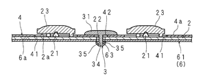
- a rivet (a retaining shaft body) is inserted into a substrate hole (opening) provided in the LED substrate and a through hole (opening) provided in the heat dissipation plate (holding plate), and the LED substrate is used as the heat dissipation plate. Fix it. In the case of screwing, a local tightening force acts on the LED substrate. However, when a rivet is used, the force acting on the LED substrate is dispersed at the large-diameter head of the rivet. Therefore, the LED substrate does not warp, and the contact area between the LED substrate and the heat radiating plate becomes larger than that in the case of screwing, and the cooling effect of the LED substrate can be enhanced.
- the rivet can suppress light leakage caused by the insertion hole (opening).
- the quality of the light source device, and thus the display device including the light source device can be improved.
- a light source device that can dissipate the heat of the circuit board satisfactorily even when the circuit board on which the light emitting element is mounted is warped due to temperature rise.
- a light source device in which a plurality of light emitting elements are mounted in the longitudinal direction and the heat of the rectangular circuit board that tends to warp in the longitudinal direction can be radiated well.
- the light source device which can form easily the heat conductor excellent in heat conductivity with the carbon containing sheet affixed on the other surface of the circuit board is provided.
- a light source device that can easily form a heat conductor excellent in heat conductivity by a layer of carbon-containing paint applied to the other surface of the circuit board.
- a display device including a direct type light source device in which a light emitting element is disposed on the other side of the display unit and excellent in heat dissipation.
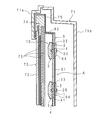
- FIG. 1 is a cross-sectional view showing a configuration of an image display device including a light source device according to Embodiment 1-1 of the present invention.
- 1 is a schematic perspective view in which a part of a light source device of an image display device according to Embodiment 1-1 of the present invention is disassembled.
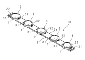
- FIG. It is a perspective view which shows the structure of the light source unit of the light source device of the image display apparatus concerning Embodiment 1-1 of this invention.
- FIG. 3 is a partially enlarged cross-sectional view showing a state where the light source unit of the image display apparatus according to Embodiment 1-1 of the present invention is held by a holder.
- FIG. 3 is a cross-sectional perspective view illustrating a state where the light source unit of the image display device according to Embodiment 1-1 of the present invention is held by a holding body. It is a cross-sectional perspective view which shows the case where a holding body is abbreviate
- FIG. 8 is a cross-sectional view taken along the line I-I-I in FIG. FIG.
- FIG. 6 is a cross-sectional view of a main part showing a state where a light source unit is held by a holder in the image display device according to Embodiment 1-2 of the present invention.
- FIG. 6 is a cross-sectional view of a main part showing a state where a light source unit is held by a holding body in the image display device according to Embodiment 1-3 of the present invention.
- FIG. 6 is a cross-sectional view of a main part showing a state where a light source unit is held by a holding body in the image display device according to Embodiment 1-4 of the present invention.
- FIG. 6 is a cross-sectional perspective view illustrating a state where the light source unit of the image display device according to Embodiment 1-5 of the present invention is held by a holding body. It is sectional drawing by the II-II line of FIG.
- FIG. 7 is a cross-sectional view of a principal part showing a state where a light source unit is held by a holding body in an image display device according to Embodiment 1-6.
- FIG. 10 is a main-portion cross-sectional view showing a state in which the light source unit is held by the holding body in the image display device according to Embodiment 1-7.
- FIG. 9 is a main part sectional view showing a state in which a light source unit is held by a holding body in an image display device according to Embodiment 1-8.
- FIG. 10 is a main part sectional view showing a state in which a light source unit is held by a holding body in an image display device according to Embodiment 1-9. It is a rear view which shows the other structure of a light source unit. It is sectional drawing which shows the other structure of a light source unit part. It is sectional drawing which shows the other structure of the light source unit part which has a heat conductor. It is a typical front view which shows the structure by which the several light source unit is juxtaposed.
- FIG. 5 is a longitudinal sectional view schematically showing a display device according to a second embodiment.
- FIG. 6 is a front view schematically showing an LED substrate fixed to a heat dissipation plate of a display device according to Embodiment 2.
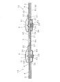
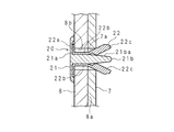
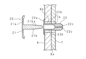
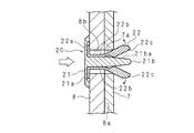
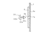
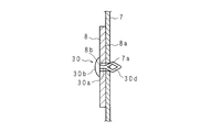
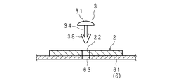
- FIG. 5 is an enlarged vertical cross-sectional view schematically showing an LED substrate fixed to a heat sink by rivets of a display device according to Embodiment 2. It is explanatory drawing explaining fixation to the heat sink of the LED board by a rivet. It is explanatory drawing explaining fixation to the heat sink of the LED board by a rivet. It is an expanded sectional view which shows the example fixed with another rivet. It is an expanded sectional view which shows the state fixed with the other rivet. It is an expanded sectional view which shows the example fixed with another rivet. It is an expanded sectional view which shows the state fixed with the other rivet.
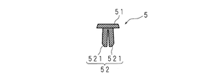
- FIG. 5 is a horizontal cross-sectional view showing a configuration of a portion fixing a circuit board and a support member included in the light source device according to Embodiment 3-1 of the present invention. It is a top view which shows the external appearance of the rivet with which the light source device which concerns on Embodiment 3-1 of this invention is provided. It is a top view which shows the external appearance of the rivet with which the light source device which concerns on Embodiment 3-1 of this invention is provided.
- FIG. 3 It is a horizontal sectional view showing the configuration of the cylindrical member of the rivet provided in the light source device according to Embodiment 3-1 of the present invention. It is a horizontal sectional view explaining a fixing procedure of a circuit board and a support member provided in the light source device according to Embodiment 3-1 of the present invention. It is a top view which shows the external appearance of the rivet with which the light source device which concerns on Embodiment 3-2 of this invention is provided. It is a top view which shows the external appearance of the rivet with which the light source device which concerns on Embodiment 3-2 of this invention is provided. FIG.
- FIG. 5 is a horizontal sectional view showing a configuration of a portion fixing a circuit board and a support member included in a light source device according to Embodiment 3-3 of the present invention. It is a top view which shows the external appearance of the rivet with which the light source device which concerns on Embodiment 3-3 of this invention is provided. It is a top view which shows the external appearance of the rivet with which the light source device which concerns on Embodiment 3-3 of this invention is provided. It is an expanded sectional view which shows the example which fixes a circuit board with another rivet. It is an expanded sectional view which shows the state fixed with the other rivet. It is an expanded sectional view which shows the example which fixes a circuit board with another rivet. It is an expanded sectional view which shows the state fixed with the other rivet.
- FIG. 6 is a perspective view illustrating a configuration of a light emitting diode substrate according to a fourth embodiment.
- FIG. 10 is a cross-sectional view illustrating an example of a fixture according to a fourth embodiment. It is sectional drawing which shows the structure of a display apparatus provided with the light source device which concerns on Embodiment 4 of this invention. It is sectional drawing which shows the operation state of the light source device which concerns on Embodiment 4 of this invention.
- FIG. 1 is an exploded perspective view showing a schematic configuration of a television receiver
- FIG. 2 is an exploded perspective view showing a schematic configuration of a liquid crystal display device.
- the television receiver includes a liquid crystal display device B, front and back cabinets C and D that are accommodated so as to sandwich the liquid crystal display device B, a power source E, a tuner F, and a stand G.
- the liquid crystal display device B has a horizontally long rectangular shape (rectangular shape) as a whole and is accommodated in a vertically placed state.
- the liquid crystal display device B includes a liquid crystal panel H that is a display panel and a backlight device A (light source device) that is an external light source.
- the liquid crystal panel H and the backlight device A are framed. Are integrally held by a bezel J or the like.
- FIG. 3 is a cross-sectional view showing a configuration of an image display device including the light source device according to Embodiment 1-1 of the present invention
- FIG. 4 is a schematic perspective view in which a part of the light source device is disassembled
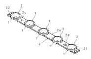
- FIG. 1 is a perspective view showing a configuration of a light source unit of a light source device of an image display device according to Embodiment 1-1.
- the image display apparatus 1 according to the present invention includes a display unit 70 (liquid crystal panel H) having a display surface for displaying an image on the front side, and a light source device A including a light source unit 10 arranged on the rear side of the display unit 70. (Backlight device) and a cabinet 71 (C, D) for concealing the peripheral portion of the display unit 70 and the rear side of the light source device A.
- the display unit 70 includes a display panel 72 having a display surface and an optical sheet 73 disposed on the rear side of the display panel 72.
- the peripheral portion of the display panel 72 is held in the front and back by a front holding frame body 74 and a rear holding frame body 75 to constitute a panel module, and the rear holding frame body 75 is a peripheral edge of the holding body 6 described later. Attached to the part.
- the optical sheet 73 is a laminate in which a relatively thick diffuser plate that diffuses light emitted from a light source and a relatively thin synthetic resin sheet such as a reflective polarizing plate, a prism sheet, and a diffuser sheet are laminated.
- the holding body 6 has a plate portion 61 and a frame portion 62 connected to the periphery of the plate portion 61, and supports the periphery of the diffusion plate on the frame portion 62.
- the cabinet 71 includes a cabinet front part 71 a that conceals the front side of the peripheral part of the display unit 70, and a deep dish-shaped cabinet rear part 71 b that conceals the peripheral part and the rear side of the light source unit 10.
- the frame portion 62 is attached by a male screw.
- the light source device A includes a light source unit 10.
- the light source unit 10 is mounted on the rear side of the display unit 70, and is mounted with a plurality of light emitting diodes 1 juxtaposed like a grid and the light emitting diodes 1 arranged side by side on one surface 2a.
- connection portions 21 and 22 for electrical connection between the other light source units 10.
- the light source device A has a through-hole 41 in which the lens 3 is disposed, and a reflection sheet 4 that reflects light emitted from the light emitting diode 1 and a connector 5 that electrically connects the light source units 10 to each other. And a holding body 6 that holds the light source unit 10.
- the reflection sheet 4 is placed on the one surface 2 a of the light emitting diode substrate 2 of the light source unit 10.
- the light source unit 10 is of two types in which five light emitting diodes 1 are mounted in a row and six light emitting diodes 1 are mounted. These are arranged in a straight line in each longitudinal direction, and are connected by a connector 5.
- the plurality of light source units 10, 10,... 10 are attached to and held by the plate portion 61 of the holding body 6.
- the light-emitting diode substrate 2 has a strip shape as shown in FIGS. 4 and 5 and is juxtaposed in the longitudinal direction and the width direction on one surface 6a of the holding body 6 having a substantially rectangular shape.
- a plurality of light emitting diodes 1 are mounted on the one surface 2a of the light emitting diode substrate 2 at appropriate intervals in the longitudinal direction, and connecting portions 21 and 22 are provided at both ends of the one surface 2a in the longitudinal direction.
- the two types of light source units 10, 10 arranged side by side are arranged so that the respective connection portions 21 are adjacent to each other, and the two adjacent connection portions 21, 21 are connected by the connector 5.
- one light source unit 10 is connected to a power circuit board through a connection portion 22 of the light emitting diode substrate 2 by a second connector described later, and the other light source unit 10 is connected to the light emitting diode substrate 2.
- 22 is connected to the control circuit board by a third connector described later.
- FIG. 6 is a partially enlarged cross-sectional view showing a state in which the light source unit 10 of the image display device according to Embodiment 1-1 of the present invention is held by the holding body 6.
- the holding body 6 As described above, for example, five or six light emitting diodes 1 are mounted apart from each other in the longitudinal direction of the light emitting diode substrate 2, and five or six lenses 3 corresponding to each light emitting diode 1. Is attached to one surface 2a with an adhesive.
- the lens 3 is spaced apart from the top of the light-emitting diode 1 and has a hemispherical light-transmitting portion 31 for diffusing light emitted by the light-emitting diode 1 in all directions, and a peripheral surface of the light-transmitting portion 31.
- a translucent portion 31 has three positioning projections 33 that project toward the light-emitting diode substrate 2 from the surface facing the one surface 2a, and determine the position of the convex portion 32 with respect to the light-emitting diode substrate 2.
- the tip of the positioning projection 33 is on the one surface 2a. It is attached with an adhesive.
- the translucent part 31 is formed to have a slightly smaller diameter than the through hole 41, the convex part 32 is formed to have a length exceeding the edge of the through hole 41, and the reflective sheet 4 penetrates between the convex part 32 and the one surface 2a.
- the peripheral edge of the hole 41 is interposed to prevent the reflection sheet 4 from being lifted with respect to the light emitting diode substrate 2.
- the positioning protrusion 33 is configured such that the distance between the convex portion 32 and the light emitting diode substrate 2 is slightly longer than the thickness of the reflection sheet 4 so that the thermal expansion of the reflection sheet 4 can be absorbed.
- the reflection sheet 4 is made of a single synthetic resin sheet having a high reflectivity and a substantially rectangular shape corresponding to the holding body 6, and through-holes 41 are opened at locations corresponding to the respective lenses 3.
- the 2nd through-hole 42 is opened in the corresponding location.
- a slit 43 cut in the radial direction is provided at the edge of the through hole 41.
- the through-hole 41 has a round shape with a slightly larger diameter than the translucent part 31, is arranged in a grid pattern, and the translucent part 31 is arranged inside.
- the slit 43 is disposed at a location corresponding to the center of the convex portion 32 and is formed longer than the length of the convex portion 32.
- the second through hole 42 has a substantially rectangular shape, and the connector 5 is inserted therethrough.
- the holding body 6 is formed by forming a metal plate, has a substantially rectangular flat plate portion 61 and a frame portion continuous to the periphery of the plate portion 61, and the light emitting diode substrate 2 is elongated on one surface 6 a of the plate portion 61. It is accommodated and held side by side in the direction and the width direction.
- the holding body 6 also serves as a heat radiating plate that radiates heat conducted from the light source unit 10 to the atmosphere.
- the plate part 61 constitutes a holding plate.
- the plate portion 61 is provided with a plurality of latching slits 63 for latching the latching portions 20 of the light-emitting diode substrate 2 described later at locations where the plate portion 61 contacts the light-emitting diode substrate 2.
- the latching slit 63 has a long hole shape in which the longitudinal direction of the plate portion 61 is the major axis direction.
- the shape of the latching slit 63 is not limited to a long hole, but may be a slit shape extending in the longitudinal direction of the plate portion 61.
- the latching slit 63 constitutes an opening.
- a concave portion 64 having a latching slit 63 is provided on one surface 6 a of the plate portion 61.
- the recessed portion 64 is recessed from the one surface 6a of the plate portion 61 toward the opposite side, has an opening on the one surface 6a side, and has a latching slit 63 on the bottom side.
- the opening of the recess 64 and the latching slit 63 are smaller than the area of the other surface 2b of the light emitting diode substrate 2, and when the light emitting diode substrate 2 is held by the plate portion 61, the light emitting diode substrate 2 causes the recess 64 to
- the opening and the latching slit 63 are configured to be covered. Therefore, external dust can be prevented from entering through the latching slit 63.
- the size of the opening of the recess 64 is such that, even after the operation of sliding the light emitting diode substrate 2 (light source unit 10) and changing the position, the light emitting diode substrate 2 always opens the opening of the recess 64. It is a size that can keep the covering state.
- the concave portion 64 having the latching slit 63 has been described as an example.
- the present invention is not limited to this, and the concave portion 64 is omitted and only the latching slit 63 is provided. Also good.
- the size of the latching slit 63 is smaller than that of the light emitting diode substrate 2 and always emits light even after the operation of sliding the light emitting diode substrate 2 (light source unit 10) and changing the position.
- the diode substrate 2 needs to have a size that can maintain the state of covering the latching slit 63.
- a power circuit board that is connected to a driver of the light emitting diode substrate 2 by a second connector and supplies a voltage to the driver is attached to one end portion in the longitudinal direction of the other surface of the plate portion 61. Is connected to a driver of the light-emitting diode substrate 2 by a third connector, and a control circuit board for controlling the driver is attached.
- a power supply circuit board that supplies a voltage to the display unit, a terminal circuit board that processes an image displayed on the display surface of the display unit, and the display unit are controlled at the longitudinal center of the other surface of the plate unit 61.
- a plurality of circuit boards such as a control circuit board are attached.
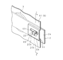
- FIG. 7 is a cross-sectional perspective view illustrating a state where the light source unit 10 of the image display apparatus according to Embodiment 1-1 of the present invention is held by the holding body 6, and FIG. 8 is a case where the holding body 6 is omitted from FIG.
- FIG. 9 is a cross-sectional perspective view taken along the line I-I--I in FIG.
- the latching portion 20 is made of metal and can be elastically deformed.
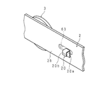
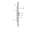
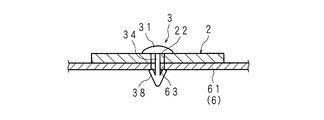
- the latching portion 20 is a rectangular plate-shaped base 20a fixed to the other surface 2b of the light-emitting diode substrate 2, and protrudes in the thickness direction of the light-emitting diode substrate 2 from one side edge of the base 20a. And a press-contacting piece 20b bent in a hook shape. A pair of the base 20a and the pressure contact piece 20b is formed. That is, an elastic restoring force in the direction of the base 20a (the other surface 2b of the light emitting diode substrate 2) is always applied to the end of the pressure contact piece 20b of the latching portion 20.
- the latching portion 20 of the light source unit 10 is hooked on the latching slit 63 and latched.
- the other surface 2b of the light emitting diode substrate 2 is in contact with the peripheral edge 6c of the recess 64, and the end of the press contact piece 20b of the hook 20 is in contact with the peripheral 65 of the hook slit 63. It is held at.
- the elastic restoring force in the direction of the other surface 2b of the light emitting diode substrate 2 is always applied to the end portion of the pressure contact piece 20b of the latch portion 20, and the pressure contact piece 20b is in contact therewith.
- a pressure contact force in the direction of the arrow in FIG. 9 is applied to the peripheral edge portion 65 of the stop slit 63 so that the light source unit 10 is brought into a stationary state in contact with the holder 6.
- the latching slit 63 not on the one surface 6a of the plate portion 61 but on the bottom of the concave portion 64 at a position moved from the one surface 6a by the depth of the concave portion 64 in the direction opposite to the direction of the elastic restoring force, As a result, the latching portion 20 is further deformed in a direction opposite to the direction of the elastic restoring force (pressure contact force), and a stronger pressure contact force can be applied to the peripheral edge portion 65 of the latch slit 63.
- the light source unit 10 of the image display device according to the first embodiment is in the major axis direction of the latching slit 63 while being held by the holding body 6, that is, the plurality of light emitting diodes 1. It is possible to slide along the one surface 6a of the plate portion 61 in the juxtaposed direction, and the light source unit 10 can be stationary on the holder 6 before and after sliding.
- the electrically adjacent light emitting diode substrates 2 (light source units 10) can be connected by the connector 5.
- the heat generated from the light emitting diode 1 of the light source unit 10 is directly conducted to the holding body 6 through the light emitting diode substrate 2 and is conducted to the holding body 6 through the plurality of latching portions 20, 20. .
- the heat conducted to the holding body 6 is dissipated into the atmosphere through the holding body 6.
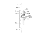
- FIG. 10 is a cross-sectional view of a main part showing a state where the light source unit 10 is held by the holding body 6 in the image display device according to Embodiment 1-2.
- a plurality of latching portions 20, 20,... 20 for holding the light source unit 10 on the holding body 6 are provided at a plurality of locations.
- the latching portion 20 is made of metal and can be elastically deformed.
- the latching portion 20 is obtained by bending a plate material.
- the strip-shaped plate material is bent to be symmetrical with respect to the center in the longitudinal direction, and is fixed to the other surface 2 b so that the lateral direction is along the longitudinal direction of the light emitting diode substrate 2.
- the latching portion 20 is connected to the base 20c that is the central portion in the longitudinal direction, and a pair of press contact pieces 20d that are connected to both opposing edges of the base 20c and extend away from the light emitting diode substrate 2. 20d.
- the pair of press contact pieces 20d and 20d face each other, and the end of one press contact piece 20d is folded back in the opposite direction to the extending direction to form a retaining member 20e.
- the latching portion 20 is formed by bending a strip-shaped plate material. Therefore, the elastic restoring force in the anti-bending direction, in other words, the direction in which the pair of press contact pieces 20d and 20d are separated from each other is obtained. work.
- the gap between the pair of press contact pieces 20 d and 20 d of the latching portion 20 of the light source unit 10 is narrowly sandwiched and inserted into the latching slit 63.
- the elastic restoring force works, the pair of pressure contact pieces 20d, 20d move in directions away from each other, and come into contact with the edge of the latching slit 63 so as to be connected to the edge of the latching slit 63.
- a pressure contact force in the direction of the arrow 10 is applied, and the light source unit 10 is brought into a stationary state in contact with the holder 6.
- the retaining member 20e of the one pressure contact piece 20d abuts on the peripheral edge portion 65 of the retaining slit 63, thereby preventing the retaining portion 20 from coming out of the retaining slit 63.
- the light source unit 10 of the image display device according to Embodiment 1-2 is in the major axis direction of the latching slit 63 while being held by the holding body 6, that is, a plurality of light emitting diodes. 1 can be slid along the one surface 6a of the plate portion 61 in the juxtaposed direction. Further, before and after sliding, the light source unit 10 can be stopped by the holding body 6, and the latching portion 20 can be prevented from coming off from the latching slit 63.
- the adjacent light emitting diode substrates 2 are separated by a predetermined distance or more that can be electrically connected by the connector 5 due to a dimensional error, a processing error, or the like. Even when the distance is closer than the interval, one or both of the light-emitting diode substrates 2 (light source unit 10) can be slid and connected by the connector 5.
- heat generated from the light emitting diode 1 of the light source unit 10 is conducted to the holding body 6 through the light emitting diode substrate 2 and the plurality of latching portions 20, 20.
- the heat conducted to the holding body 6 is dissipated into the atmosphere through the holding body 6.
- the hooking portion 20 is formed by bending a strip-like plate material that can be elastically deformed has been described as an example, but the present invention is not limited thereto.
- the pair of press contact pieces 20d and 20d may not have the same shape and size.
- the base 20c may be omitted, and only the two pressure contact pieces 20d, 20d may be separated from each other and disposed opposite to the other surface 2b of the light emitting diode substrate 2.
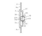
- FIG. 11 is a cross-sectional view of the main part showing a state where the light source unit 10 is held by the holding body 6 in the image display apparatus according to Embodiment 1-3 of the present invention.
- a plurality of latching portions 20, 20,... 20 for holding the light source unit 10 on the holding body 6 are provided at a plurality of locations.
- the latching portion 20 is made of metal and can be elastically deformed.
- the latching portion 20 is obtained by bending a plate material.
- the strip-shaped plate material is bent to be symmetrical with respect to the center in the longitudinal direction, and is fixed to the other surface 2 b so that the lateral direction is along the longitudinal direction of the light emitting diode substrate 2.
- the latching portion 20 includes a flat base 20f formed at the center in the longitudinal direction, and a pair of bases 20f that are connected to both opposing edges of the base 20f and extend away from the light emitting diode substrate 2.
- the pressure contact pieces 20g and 20g, and the stoppers 20h and 20h provided at the ends of the pressure contact pieces 20g and 20g, respectively.
- the pair of pressure contact pieces 20g, 20g face each other and are bent inwardly facing each other.
- the stoppers 20h and 20h are formed by folding the end portions of the pressure contact pieces 20g and 20g in the opposite direction to the extending direction and then bending the end portions in the extending direction.
- the latching portion 20 is formed by bending a strip-shaped plate material, the elastic restoring force in the anti-bending direction, in other words, the direction in which the pair of press contact pieces 20g and 20g are separated from each other is obtained. work.
- Embodiment 1-3 a state where the light source unit 10 is held by the holding body 6 will be described in detail.
- the gap between the pair of press contact pieces 20g, 20g of the latching portion 20 of the light source unit 10 is narrowly inserted and inserted into the latching slit 63.
- the elastic restoring force works, the pair of pressure contact pieces 20g, 20g move in directions away from each other, and come into contact with the edge of the latching slit 63 so that the edge of the latching slit 63 can be seen.
- a pressure contact force in the direction of the arrow 11 is applied to bring the light source unit 10 into a stationary state in contact with the holder 6.
- the stoppers 20 h and 20 h prevent the hooking part 20 from coming out of the hooking slit 63 because the opposite surfaces of the hooking faces 20 a and 20 h are in contact with the peripheral edge 65 of the hooking slit 63.
- the light source unit 10 of the image display device according to Embodiment 1-3 is in the major axis direction of the latching slit 63 while being held by the holding body 6, that is, a plurality of light emitting diodes. 1 can be slid along the one surface 6a of the plate portion 61 in the juxtaposed direction. Further, before and after sliding, the light source unit 10 can be stopped by the holding body 6, and the latching portion 20 can be prevented from coming off from the latching slit 63.
- the adjacent light emitting diode substrates 2 are separated by a predetermined distance or more that can be electrically connected by the connector 5 due to a dimensional error, a processing error, or the like. Even when the distance is closer than the interval, one or both of the light-emitting diode substrates 2 (light source unit 10) can be slid and connected by the connector 5.
- fever emitted from the light emitting diode 1 is conducted to the holding body 6 through the light emitting diode board
- the heat conducted to the holding body 6 is dissipated into the atmosphere through the holding body 6.
- FIG. 12 is a cross-sectional view of a main part showing a state where the light source unit 10 is held by the holding body 6 in the image display device according to Embodiment 1-4 of the present invention.
- the other surface 2b of the light emitting diode substrate 2 is provided with a plurality of latching portions 20, 20,... 20 for holding the light source unit 10 on the holder 6.
- the latching portion 20 includes a base 20i made of a rectangular plate whose one surface is fixed to the other surface 2b, and a spring portion 20j protruding from the other surface of the base 20i in the thickness direction of the base 20i. And a pressure contact piece 20k connected to the end of the spring portion 20j.
- the pressure contact piece 20k is made of an elastically deformable metal and has a rod shape. One end of the pressure contact piece 20k is bent in a hook shape, and the other end is connected to the end of the spring portion 20j.
- the spring portion 20j is a coil spring and is configured such that the length of the spring portion 20j in the projecting direction is shorter than the depth D of the concave portion 64 of the holding body 6.
- the pressure contact piece 20k may be formed by bending the end of the spring portion 20j of the coil spring.
- Embodiment 1-4 the state where the light source unit 10 is held by the holding body 6 will be described in detail.
- the latching portion 20 of the light source unit 10 is inserted into the latching slit 63, the pressure contact piece 20 k is hooked on the peripheral edge 65 of the latching slit 63, and the latching portion 20 is latched on the latching slit 63.
- the pressure contact piece 20k is in the direction of the light emitting diode substrate 2 with one end portion thereof in contact with the peripheral edge portion 65 of the latching slit 63.
- the pressure contact piece 20k applies a pressure contact force in the direction of the arrow in FIG. 12 to the peripheral edge portion 65 of the abutting latching slit 63, and the light source unit 10 is in contact with the holding body 6. Keep it stationary. In the state where the pressure contact piece 20k is hooked on the peripheral edge portion 65 of the latching slit 63, the elastic restoring force always acts on the pressure contact piece 20k, so that the latching portion 20 can be prevented from coming off from the latching slit 63.
- the light source unit 10 of the image display device according to Embodiment 1-4 is in the major axis direction of the latching slit 63 while being held by the holding body 6, that is, a plurality of light emitting diodes. 1 can be slid along the one surface 6a of the plate portion 61 in the juxtaposed direction. Further, before and after sliding, the light source unit 10 can be stopped by the holding body 6, and the latching portion 20 can be prevented from coming off from the latching slit 63.
- the adjacent light emitting diode substrates 2 are separated by a predetermined distance or more that can be electrically connected by the connector 5 due to a dimensional error, a processing error, or the like. Even when the distance is closer than the interval, one or both of the light-emitting diode substrates 2 (light source unit 10) can be slid and connected by the connector 5.
- fever emitted from the light emitting diode 1 is conducted to the holding body 6 through the light emitting diode board
- the heat conducted to the holding body 6 is dissipated into the atmosphere through the holding body 6.
- FIG. 13 is a cross-sectional perspective view illustrating a state in which the light source unit 10 of the image display apparatus according to Embodiment 1-5 of the present invention is held by the holding body 6, and FIG. 14 is taken along the line II-II in FIG. It is sectional drawing.
- the latching portion 20 is made of metal and can be elastically deformed.
- the latching portion 20 is a rectangular plate-shaped base 20a fixed to the other surface 2b of the light-emitting diode substrate 2, and protrudes in the thickness direction of the light-emitting diode substrate 2 from one side edge of the base 20a.
- the portion is bent in a hook shape, and the end portion has a pressure contact piece 20b arranged to face the base 20a.
- An anti-slip convex portion 20m that restricts the sliding of the latching portion 20 (the press contact piece 20b) is provided on one surface of the end portion of the press contact piece 20b facing the base 20a.
- the non-slip convex portion 20m has a hemispherical shape, and when the latching portion 20 is latched by the latch slit 63, the non-slip convex portion 20m abuts on a non-slip concave portion 66 described later.
- a pair of base 20a, anti-slip convex part 20m and pressure contact piece 20b is formed, and the base 20a (light emitting diode substrate 2) is always provided at the end of the pressure contact piece 20b of the latching part 20 including the anti-slip convex part 20m.
- the elastic restoring force in the direction of the other surface 2b) is configured to work. That is, when the latching portion 20 is latched by the latching slit 63, the pressure contact piece 20 b applies a pressure contact force in the arrow direction of FIG. 14 to the peripheral edge portion 65 of the latching slit 63 in contact with the light source unit 10. Is held still in contact with the holding body 6.
- the peripheral edge 65 of the latching slit 63 is provided with a plurality of anti-slip recesses 66, 66, 66, 66 for restricting the sliding of the latching part 20 (pressure contact piece 20b). Specifically, when the latching portion 20 is latched by the latching slit 63, a plurality of anti-slip recesses 66 having a shape following the anti-slip projection 20m are provided at positions where the latch 20 contacts the anti-slip projection 20m. It is formed in the place.
- the anti-slip convex portion 20 m of the latching portion 20 engages with the anti-slip concave portion 66 of the peripheral edge 65 of the latching slit 63 and latches.
- the sliding of the part 20 in the vertical and horizontal directions is restricted.
- the non-slip convex portion 20m is detached from the non-slip concave portion 66 and the engagement is released. Therefore, the light emitting diode substrate 2 can be slid in the direction of the force.
- the anti-slip recess 66 is a depression
- the present invention is not limited to this.
- the peripheral edge 65 of the latch slit 63 is arranged in the thickness direction. It may be a through-hole or a non-slip projection.
- FIG. 15 is a cross-sectional view of a main part showing a state where the light source unit 10 is held by the holding body 6 in the image display apparatus according to Embodiment 1-6.
- a latching slit 63 is opened in the plate portion 61, and instead of the latching portion 20 being fixed to the light emitting diode substrate 2, a latching slit 23 is opened in the light emitting diode substrate 2, and the plate portion 61 is arranged. In this configuration, the latching portion 60 is fixed.
- a long hole-like latching slit 23 is provided on both sides in the longitudinal direction of the light emitting diode substrate 2 having a strip shape.
- the latching slit 23 constitutes an opening.
- a latching portion 60 to be inserted into the latching slit 23 is fixed to a portion of the plate portion 61 facing the light emitting diode substrate 2.
- the latching portion 60 is substantially L-shaped and made of a metal plate that can be elastically deformed. One end of the latching portion 60 is fixed to the plate portion 61, and the other end side press-contact portion 60b faces the one surface 2a of the light-emitting diode substrate 2.
- the light emitting diode substrate 2 is configured to be in pressure contact with the plate portion 61. Further, a highly reflective material is applied to the surface that does not oppose the one surface 2 a of the latching portion 60 and the edge of the latching slit 23, thereby avoiding uneven brightness due to the latching portion 60.
- the pressure contact portion (pressure contact piece) constitutes an engagement portion.
- the latching portion 60 is inserted into the latching slit 23 of the light emitting diode substrate 2, and the light emitting diode substrate 2 is moved in the width direction.
- the pressure contact portion By slightly moving the pressure contact portion, the pressure contact portion is bent and pressed against the one surface 2a of the light emitting diode substrate 2, and a sliding resistance is applied to the light emitting diode substrate 2 by the elastic restoring force of the pressure contact portion.
- the light emitting diode substrate 2 can be slid in the longitudinal direction of the latching slit 23 with respect to the latching portion 60.
- the latching part 60 fixed to the plate part 61 may be any latching part in any of Embodiments 1-1 to 1-5.
- Other configurations are the same as those in Embodiment 1-1 to Embodiment 1-5, and the same reference numerals are given to the same portions as those in Embodiment 1-1 to Embodiment 1-5. Detailed description is omitted.
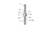
- FIG. 16 is a cross-sectional view of a main part showing a state where the light source unit 10 is held by the holding body 6 in the image display apparatus according to Embodiment 1-7.
- a non-flexible retaining projection 8 is provided instead of the latching portion 20 capable of elastic deformation.
- a long hole-like latching slit 23 is provided on both sides in the longitudinal direction of the light emitting diode substrate 2 having a strip shape.
- the latching slit 23 constitutes an opening.
- a plurality of mounting holes 67 for mounting the retaining projections 8 to be inserted into the latching slits 23 are formed at positions of the plate portion 61 facing the light emitting diode substrate 2.
- the retaining projection 8 is a small-diameter shaft portion 8 a that is screwed into the mounting hole 67, and is connected to the small-diameter shaft portion 8 a via a step portion 8 b and is inserted into the latching slit 23 so as to be relatively movable. And a stepped male screw having a retaining portion 8d that is connected to the large-diameter shaft portion 8c and engages with an edge portion of the latching slit 23 to apply sliding resistance to the light emitting diode substrate 2.
- the retaining convex portion 8 in the state where the light emitting diode substrate 2 is placed on the plate portion 61, the retaining convex portion 8 is inserted from the one surface 2a side of the light emitting diode substrate 2 into the latching slit 23, and the small diameter shaft portion.
- the retaining convex portion 8 By screwing 8a into the mounting hole 67, the retaining convex portion 8 is fixed to the plate portion 61, the retaining portion 8d engages with the edge of the latching slit 23, and the plate portion 61 of the light emitting diode substrate 2 Movement in the direction of separation, in other words, withdrawal is prevented.
- the large-diameter shaft portion 8c is disposed in the retaining slit 23, and the light-emitting diode substrate 2 can slide with respect to the large-diameter shaft portion 8c.
- the sliding resistance by the retaining portion 8d allows the light-emitting diode substrate 2 to slide when the light-emitting diode substrate 2 is slid, and keeps the light-emitting diode substrate 2 stationary when the sliding operation is stopped. It is the extent that can be.
- the retaining protrusion 8 is fixed to the plate portion 61, the heat of the light-emitting diode substrate 2 is more efficiently radiated by forming the retaining protrusion 8 with a material having high thermal conductivity. And the expansion of the light emitting diode substrate 2 can be further suppressed. Further, by providing a sheet-like heat conductor between the light emitting diode substrate 2 and the holding body 6, the heat of the light emitting diode substrate 2 can be radiated more efficiently.
- the stepped male screw as the retaining protrusion 8 may be fixed to the light emitting diode substrate 2 in addition to being fixed to the plate portion 61.
- the light emitting diode substrate 2 is provided with a mounting hole into which the small-diameter shaft portion 8a is screwed, and the plate portion 61 is provided with a latching slit.
- the large diameter shaft portion 8c disposed in the latch slit 23 is composed of a low reflective material, or the large diameter shaft portion.
- the retaining protrusion 8 may be a stepped pin having the same shape as the stepped male screw instead of the stepped male screw.
- Other configurations are the same as those of the embodiment 1-1, and the same parts as those of the embodiment 1-1 are denoted by the same reference numerals and detailed description thereof is omitted.
- FIG. 17 is a cross-sectional view of a main part showing a state where the light source unit 10 is held by the holding body 6 in the image display apparatus according to Embodiment 1-8.
- the light emitting diode substrate 2 and the holding body 6 are used instead of slidably holding the light source unit 10 by the latching portion 20 and the retaining projection 8 fixed to the light emitting diode substrate 2 or the holding body 6, the light emitting diode substrate 2 and the holding body 6 are used.
- the light source unit 10 is configured to be slidably held by a retaining shaft body 9 formed separately.
- a long hole-like latching slit 23 is provided on both sides in the longitudinal direction of the light emitting diode substrate 2 having a strip shape.
- the latching slit 23 constitutes an opening.
- a plurality of insertion holes 68 into which the retaining shaft body 9 to be inserted into the latching slit 23 is inserted are formed at locations facing the light emitting diode substrate 2 of the plate portion 61.
- the retaining shaft body 9 has a small-diameter head 91a at one end and a flexible cylinder 91b having a flexible portion 91b that can be bent in the radial direction at the other end, and is opposed to the small-diameter head 91a in the axial length direction.
- the flexible cylinder 91 has a cylindrical portion 91c having a slightly larger diameter than the insertion hole 68 and a small-diameter head portion 91a having a diameter larger than the width of the latching slit 23, and the cylindrical portion 91c.
- a plurality of circumferential positions are provided with slits 91d, and a portion between the slits 91d is a flexible portion 91b.
- the inside of the flexible portion 91b is formed to have a slightly small diameter, and the outer peripheral portion of the pin 92 fitted in the flexible tube 91 abuts on the inside of the flexible portion 91b, and the flexible portion 91b bends radially outward. It is supposed to be.
- the pin 92 is provided with a large-diameter head 92a having a larger diameter than the small-diameter head 91a at one end of the columnar portion 92b.
- the flexible cylinder 91 is inserted into the latching slit 23 and the fitting hole 68 from the one surface 2a side of the light emitting diode substrate 2 with the light emitting diode substrate 2 placed on the plate portion 61. After the small-diameter head portion 91 a of the flexible tube 91 contacts the one surface 2 a of the light emitting diode substrate 2, the pin 92 is inserted into the flexible tube 91 from the one surface 2 a side of the light emitting diode substrate 2.
- the tip end portion of the pin 92 contacts the inside of the flexible portion 91b, the flexible portion 91b bends radially outward, and is hooked on the edge of the insertion hole 68, thereby preventing the flexible tube 91 from being pulled out.
- the pin 92 is prevented from being pulled out by the contact resistance of the pin 92 with the inner surface of the flexible portion 91, and the large-diameter head portion 92 a of the pin 92 contacts the one surface 2 a of the light emitting diode substrate 2.
- the small-diameter head 91a of the flexible tube 91 and the large-diameter head 92a of the pin 92 are in contact with the one surface 2a of the light-emitting diode substrate 2, the stress acting on the light-emitting diode substrate 2 from the retaining shaft body 9 is small. Dispersed by the portion 91a and the large-diameter head 92a, the entire head in the width direction of the light-emitting diode substrate 2 is pushed as compared with the case where the head is small-diameter, while avoiding distortion and warping of the light-emitting diode substrate 2, The light emitting diode substrate 2 can be slid.
- the flexible cylinder 91 of the retaining shaft body 9 is made of a low reflection material, or the flexible cylinder 91 has a low reflection color. It is possible to avoid the light emitted from the diode from reaching the other surface side of the support 6 from the latching slit 23 and the fitting hole 68.
- the retaining shaft body 9 has the small-diameter head portion 91a and the large-diameter head portion 92a in contact with the one surface 2a of the light-emitting diode substrate 2, so that the retaining shaft body 9 is formed of a material having high thermal conductivity.
- the heat of the light emitting diode substrate 2 can be radiated more efficiently, and the expansion of the light emitting diode substrate 2 can be further suppressed. Further, by providing a sheet-like heat conductor between the light emitting diode substrate 2 and the holding body 6, the heat of the light emitting diode substrate 2 can be radiated more efficiently.
- FIG. 18 is a cross-sectional view of a principal part showing a state where the light source unit 10 is held by the holding body 6 in the image display apparatus according to Embodiment 1-9.
- a heat conductor 30 is fixed between the light emitting diode substrate 2 and the holding body 6.
- the heat conductor 30 is made of a carbon-containing sheet, and is attached to the entire other surface 2b of the light emitting diode substrate 2 having a strip shape.
- the carbon-containing sheet 9 is more excellent in thermal conductivity than the light-emitting diode substrate 2, and the thermal conductivity of the carbon-containing sheet 9 is larger than the thermal conductivity of the light-emitting diode substrate 2.
- the heat generated in the light emitting diode 1 can be radiated from the light emitting diode substrate 2 to the thermal conductor 30 more efficiently, and radiated from the thermal conductor 30 to the holding body 6. Therefore, the expansion of the light emitting diode substrate 2 can be further suppressed, and the sliding of the light emitting diode substrate 2 due to the expansion can be further suppressed.
- the heat conductor 30 is fixed to the other surface 2b of the light emitting diode substrate 2 or one surface 6a of the support 6 by an appropriate fixing means.
- the heat conductor 30 is formed to have a size that comes into full contact with the other surface 2b of the light emitting diode substrate 2 having a strip shape.
- the longitudinal direction both ends of the light emitting diode substrate 2 are held by the plate portion 61 by any one of the portion 20, the retaining protrusion 8, and the retaining shaft body 9, and a part of the light emitting diode substrate 2 is fixed with a male screw or the like. Is done.
- the light-emitting diode substrate 2 is slidable, it is considered that the light-emitting diode substrate 2 is not warped, but actually, the light-emitting diode substrate 2 is partially distorted during sliding, and the light-emitting diode substrate 2 Since the same problem as the warpage of 2 occurs, a part of the light emitting diode substrate 2 is fixed, so that the distortion of the light emitting diode substrate 2 can be suppressed.
- Embodiment 1-10 19 is a rear view showing another configuration of the light source unit
- FIG. 20 is a sectional view showing another configuration of the light source unit portion
- FIG. 21 is a sectional view showing another configuration of the light source unit portion having a heat conductor.
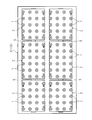
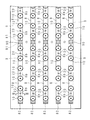
- 22 is a schematic front view showing a configuration in which a plurality of light source units 10 are juxtaposed.
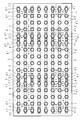
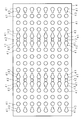
- the light emitting diode substrate 2 has a strip shape and a plurality of light emitting diodes 1 are arranged in a line.
- the configuration may include a light emitting diode substrate 2 in which a plurality of light emitting diodes 1 are arranged in a plurality of rows, and the form of the light emitting diode substrate 2 is not particularly limited.
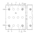
- a hooking portion 20 is provided on the other side of the square portion of the light emitting diode substrate 2 in which a plurality of light emitting diodes 1 are arranged in a plurality of rows on one surface, and the portion corresponding to the square portion of the light emitting diode substrate 2 Is provided with a latching slit 63.
- the pressure contact piece 20b of each of the latching portions 20 faces the same direction, and the latching portion 20 is latched by the latching slit 63 when the light emitting diode substrate 2 is slid in one direction. Yes.
- the light emitting diode substrates 2 are arranged in a plurality of rows separated in two directions, and the adjacent light emitting diode substrates 2 on the rows are connected by a connector 5.
- a sheet-like heat conductor 30 may be provided between the light emitting diode substrate 2 and the holding body 6.
- the heat conductor 30 having the same shape as that of the light-emitting diode substrate 2 shown in FIG. 19 is fixed to the other surface 2b of the light-emitting diode substrate 2, and a latching portion is provided at a position corresponding to the latch slit 63 of the heat conductor 30. 20 is provided.
- the latching portion 20 may pass through the thermal conductor 30 and be fixed to the light emitting diode substrate 2. Further, in place of the latching portion 20, the retaining projection 8 and the retaining shaft body 9 may be used.
- Embodiments 1-6 to 1-9 may be combined with any of Embodiments 1-1 to 1-10.
- the light emitting diode substrate 2 is described as an example in which the light emitting diode substrate 2 is held on the holding body 6 by any of the plurality of latching portions 20, 20,...
- the present invention is not limited to this, and the latching portion 20, the retaining convex portion 8, and the retaining shaft body 9 may be shared.
- FIG. 23 is a longitudinal sectional view schematically showing the configuration of the display device.
- reference numeral 1 denotes a rectangular display panel having a liquid crystal
- the display panel 1 is configured to display an image by adjusting a light transmittance by controlling a voltage applied to the liquid crystal.
- the display panel 1 is sandwiched between a front holding frame body 2 and a rear holding frame body 3, and is accommodated in a rectangular frame-shaped front cabinet 4.
- the front cabinet 4 is disposed around the front holding frame 2 and the rear holding frame 3.
- the front cabinet 4 has a rectangular opening, and the dimension of the opening corresponds to the display panel 1.
- On the rear side of the display panel 1, a plurality of optical sheets 5 for condensing the light of the LED 9 described later toward the display panel 1 are provided.
- a diffusion plate 6 for uniformly diffusing the light of the LED 9 is provided on the rear side of the optical sheet 5.
- the diffusing plate 6 is supported by an edge portion of a deep dish type heat radiating plate 7.
- a plurality of LED substrates 8 are arranged in parallel on the front surface of the heat radiating plate 7, and a film-shaped heat radiation pattern 8 a made of a heat conductive material, for example, a metal is formed on the rear surface of the LED substrate 8.
- a plurality of LEDs 9, 9,... 9 are mounted on the front surface of the LED substrate 8, and lenses 10, 10,. ⁇ 10 are arranged.
- Three projections 10 a, 10 a, 10 a projecting toward the LED substrate 8 side are juxtaposed in the circumferential direction on the periphery of the lens 10, and the tip of the projection 10 a is attached to the front surface of the LED substrate 8 with an adhesive. ing.
- Supporters for supporting the deep dish type reflection sheet 11 are provided on the left and right sides of the heat radiating plate 7, respectively.
- a plurality of holes 11 a into which the lens 10 is inserted are opened on the bottom surface of the reflection sheet 11. Each lens 10 projects forward through the hole 11a.
- FIG. 24 is a front view schematically showing the LED substrate 8 fixed to the heat radiating plate 7
- FIG. 25 is an enlarged vertical sectional view schematically showing the LED substrate 8 fixed to the heat radiating plate 7 by rivets (holding means).
- the heat sink 7 has a rectangular shape, and as shown in FIG. 24, strip-shaped LED substrates 8 are juxtaposed in the longitudinal direction and the width direction of the heat sink 7 on the front surface of the heat sink 7. Yes.
- Connection portions 81 and 82 are provided at both ends of the front surface of the LED substrate 8 in the longitudinal direction.
- the connecting portions 81 and 81 are opposed to each other in the longitudinal direction and are connected by a connector 90.
- the connection part 82 located in the longitudinal direction edge part of the heat sink 7 is connected to the drive board
- the LED substrate 8 has a plurality of substrate holes 8b, 8b,..., 8b arranged at equal intervals along the longitudinal direction of the LED substrate 8.
- the substrate hole 8b has an elliptical shape extending in the longitudinal direction.
- the heat radiating plate 7 has a plurality of through holes 7a at positions corresponding to the substrate holes 8b.
- the diameter of the through hole 7a is substantially equal to the short diameter of the elliptical substrate hole 8b.
- a rivet 20 made of, for example, metal or carbon is inserted into the substrate hole 8 b and the through hole 7 a, and the LED substrate 8 is fixed to the heat sink 7 by the rivet 20.
- the rivet 20 includes a receiving rivet (flexible cylinder) 22 and an insertion rivet (pin) 21.
- the receiving rivet 22 includes a hooking portion 22a (small-diameter head) having an annular shape with a diameter larger than the short diameter of the substrate hole 8b, and the outer peripheral portion of the hooking portion 22a is at the edge of the substrate hole 8b. It is hanging.
- a plurality of elastic portions 22b are juxtaposed in the circumferential direction on the inner peripheral portion of the latching portion 22a. The elastic portion 22b protrudes along the axial direction of the latching portion 22a and is inserted through the substrate hole 8b and the through hole 7a.
- the axial dimension of the elastic part 22b is larger than the axial dimension of the substrate hole 8b and the through hole 7a, and the protruding end of the elastic part 22b extends from the through hole 7a in the axial direction.
- a contact portion 22c extending radially inward of the latching portion 22a is provided integrally with the elastic portion 22b, and there is a gap between the corresponding contact portions 22c and 22c. Yes.
- An insertion shaft 21b which will be described later, is in contact with the inside of the contact portion 22c, and the elastic portion 22b is curved outward by the contact of the insertion shaft 21b, and the elastic portion 22b contacts the edge portion of the through hole 7a. ing. For this reason, the LED substrate 8 and the heat sink 7 are sandwiched between the hooking portion 22a and the elastic portion 22b.
- the insertion rivet 21 includes a head (a large diameter head) 21a having a diameter larger than that of the hooking portion 22a.
- An insertion shaft 21b perpendicular to the head 21a is provided at the center of the head 21a. It is.
- a taper 21ba is formed at the distal end portion of the insertion shaft 21b so that the diameter of the insertion shaft 21b decreases toward the distal end.
- the diameter of the insertion shaft 21b in the vicinity of the head 21a is substantially the same as the inner diameter of the latching portion 22a, and is larger than the dimension between the contact portions 22c when the insertion shaft 21b is not inserted. .
- FIG. 26A and FIG. 26B are explanatory views for explaining fixing of the LED substrate 8 to the heat radiating plate 7 by the rivet 20.
- the LED board 8 When fixing the LED board 8 to the heat sink 7, first, the LED board 8 is placed on the heat sink 7 so that the board hole 8 b is positioned on the through hole 7 a and the connection portions 81 and 81 can be connected to each other. Deploy. As described above, the substrate hole 8b is formed in an elliptical shape extending in the longitudinal direction (lateral direction), and adjustment in the lateral direction for connecting the connection portions 81 and 81 can be easily performed. Next, the receiving rivet 22 is inserted into the board hole 8b and the through hole 7a from the LED board 8 side, and the latching part 22a is latched to the edge part of the board hole 8b as shown in FIG. 26A. At this time, since the insertion rivet 21 is not inserted into the receiving rivet 22, the elastic portion 22b extends along the axial direction and is disposed in the substrate hole 8b and the through hole 7a.
- the insertion shaft 21b of the insertion rivet 21 is inserted into the hooking portion 22a, and the tip end portion of the insertion shaft 21b is inserted into the gap between the contact portions 22c. Since the taper 21ba is formed at the distal end portion of the insertion shaft 21b, the gap is gradually expanded, and the elastic portion 22b is curved outward as shown by the arrow in FIG. Contact the edge.
- the insertion rivet 21 is received and inserted into the rivet 22 until the head 21a comes into contact with the latching portion 22a, and an appropriate pressure is applied between the elastic portion 22b and the latching portion 22a to dissipate heat from the LED board 8.
- the plate 7 is brought into close contact.
- the rivet 20 is inserted into the substrate hole 8 b provided in the LED substrate 8 and the through hole 7 a provided in the heat sink 7 to fix the LED substrate 8 to the heat sink 7.
- a local tightening force acts on the LED board 8
- the force acting on the LED board 8 is dispersed by the large-diameter head 21 a of the rivet 20.
- the Therefore, the LED substrate 8 does not warp, and the contact area between the LED substrate 8 and the heat radiating plate 7 becomes larger than that when screwed, and the LED substrate 8 can be reliably cooled. Further, the heat generated in the LED substrate 8 is efficiently conducted to the heat radiating plate 7 through the pattern for heat dissipation.
- the LED substrate 8 can be fixed to the heat sink 7 while positioning the LED substrate 8 in consideration of the connection between the LED substrates 8 and the dimensional error of the LED substrate 8.
- the elastic portion 22b is inserted into the substrate hole 8b and the through hole 7a with the hook portion 22a being hooked on the edge portion of the substrate hole 8b, and the insertion shaft 21b is inserted into the hook portion 22a to contact the contact portion 22c. Abut. At this time, the elastic portion 22b is curved outward in the radial direction by elastic deformation, and the curved elastic portion 22b contacts the edge portion of the through hole 7a. Therefore, the LED substrate 8 and the heat radiating plate are formed by the latching portion 22a and the elastic portion 22b. 7 is clamped at an appropriate pressure.
- the heat generated in the LED substrate 8 can be efficiently conducted to the heat sink 7 via the rivet 20.
- the LED substrate 8 is fixed by the rivet 20 having the insertion rivet 21 and the receiving rivet 22, but the LED substrate 8 is fixed by the insertion rivet type rivet 30. It is good.
- 27A and 28A are enlarged sectional views showing an example of fixing with another rivet 30, and FIGS. 27B and 28B are enlarged sectional views showing a state fixed with another rivet 30.
- FIG. The rivet 30 in FIG. 27A has a head 30b continuous with one end of the shaft portion 30a and a retaining portion (engagement portion) 30c extending from the other end of the shaft portion 30a toward the head 30b and having flexibility. It is integrally molded with a synthetic resin material.
- the retaining portion 30c bends toward the peripheral surface side of the shaft portion 30a, and when the retaining portion 30c pulls out the substrate hole 8b and the through hole 7a, elastic recovery is performed. The retaining portion 30c is restored by force, and the retaining portion 30c is hooked to the edge of the through hole 7a.
- the rivet 30 in FIG. 28A extends from the other end of the head portion 30b and the shaft portion 30a continuous to one end of the shaft portion 30a, and further has a flexible retaining portion (engagement) that forms a substantially rhombic shape that is further tapered.
- Part) 30d and is integrally formed of a synthetic resin material.
- the retaining portion 30d bends, and when the retaining portion 30d pulls out the substrate hole 8b and the through hole 7a, the retaining portion 30d is restored by an elastic restoring force.
- the retaining portion 30d is hooked on the edge of the through hole 7a.
- the assembly workability can be improved in the same manner as the case where the rivet 20 is provided, and moreover, it can be made cheaper than the rivet 20.
- the LED substrate 8 is fixed by the rivet 20 and the rivet 30. Alternatively, the LED substrate 8 may be fixed by screws.
- a stepped screw having a head that engages the edge and applies resistance to the LED substrate 8 is used.
- the screw head is formed as large as the head 21a of the insertion rivet 21, and the screw is formed of a material having high thermal conductivity, so that the heat of the LED substrate 8 can be radiated more efficiently.
- the insertion shaft 21b is inserted from the LED substrate 8 side, but may be configured to be inserted from the heat sink 7 side.
- the rivet 20 may be made of a synthetic resin.
- FIG. 29 is a longitudinal sectional view showing a partial configuration of display device 7 including light source device 1 according to Embodiment 3-1 of the present invention.
- the left-right direction in FIG. 29 is equal to the front-rear direction of the display device 7 and thus the light source device 1.
- FIG. 30 is a horizontal cross-sectional view illustrating a configuration of a portion where the circuit board 2 and the support member 6 included in the light source device 1 are fixed.
- the vertical direction in FIG. 30 is equal to the front-rear direction of the display device 7 and thus the light source device 1.
- the front surface 2a of the circuit board 2 is provided with a plurality of lenses 23, 23,.
- Each lens 23 has a circular shape and is disposed to face the top of the light emitting unit 21.
- the lens 23 diffuses the light generated by the light emitting unit 21.
- First and second connection portions (not shown) are mounted on the right end portion and the left end portion of each circuit board 2.
- the support member 6 has a rectangular plate shape formed by molding a metal plate, and includes a rectangular flat plate-like flat plate portion 61 and a frame portion 62 that is continuous with the periphery of the flat plate portion 61.
- the support member 6 supports the circuit boards 2, 2,. Therefore, circuit boards 2, 2,... Are fixed to the front surface 6a of the flat plate portion 61 in a state of being juxtaposed in a matrix. As a result, the light emitting units 21, 21,... Are arranged in a matrix.
- a power circuit board (not shown) for supplying power to each of the circuit boards 2, 2,... Is attached to the right end portion of the support member 6.
- a control circuit board for controlling the operation of each of the circuit boards 2, 2,... Is attached to the left end portion of the support member 6.
- the first connection part of the circuit board 2 arranged on the left side and the second connection part of the circuit board 2 arranged on the right side are the first.
- the 2nd connection part is electrically connected through the 1st connector which bridges.
- each of the first connection portions mounted on the rightmost circuit boards 2, 2,... In the flat plate portion 61 is electrically connected to the power supply circuit board via a second connector (not shown).
- each of the second connection portions mounted on the leftmost circuit boards 2, 2,... In the flat plate portion 61 is electrically connected to the control circuit board via a third connector (not shown).
- Each connector has a cream color which is a highly reflective color.
- the reflection sheet 4 is made of a synthetic resin sheet, and at least the front surface 4a of the reflection sheet 4 has white which is a highly reflective color.
- the reflection sheet 4 has a rectangular shape corresponding to the shape of the support member 6, and circular through holes 41, 41,... Are provided at positions corresponding to the positions where the lenses 23, 23,. Is formed.
- the reflection sheet 4 is in contact with the front surfaces 2a, 2a,... Of the circuit boards 2, 2,..., And the lenses 23, 23,. 6 is fixed.
- the light source device 1 is disposed on the back side of the display unit 70 so as to illuminate the display unit 70.
- the display unit 70 has a rectangular shape and includes a display panel 701 and an optical sheet 702.
- the display panel 701 is, for example, a liquid crystal display panel, and the front surface of the display panel 701 constitutes a display surface 7a for displaying an image.
- the optical sheet 702 is disposed between the display panel 701 and the lenses 23, 23,... Facing the back surface of the display panel 701, and diffuses the light generated by the light emitting units 21, 21,.
- the optical sheet 702 is a laminate in which a relatively thick diffuser plate and a relatively thin synthetic resin sheet using a reflective polarizing plate, a prism sheet, or a diffuser sheet are laminated.
- the display panel 701 forms a panel module by sandwiching the peripheral portion of the display panel 701 between the front frame body 72 and the rear frame body 73 in the front-rear direction.
- the rear frame 73 is attached to the frame 62 of the support member 6, and the optical sheet 702 is sandwiched between the rear frame 73 and the frame 62 in the front-rear direction.
- the cabinet 71 accommodates the panel module, the optical sheet 702, and the light source device 1 in a state where the display surface 7a is exposed from the front opening and the portions other than the display surface 7a are concealed.
- the cabinet 71 is formed with heat exhaust ports 711, 711,... So that heat generated inside the cabinet 71 is easily discharged to the outside.
- a plurality of circuit boards are attached to the center in the left-right direction on the back surface of the flat plate portion 61 of the support member 6. These circuit boards are a power supply circuit board that supplies power to the display panel 701, an image processing circuit board that processes an image to be displayed on the display surface 7a, a control circuit board that controls the operation of the display panel 701, and the like.
- FIGS. 31A and 31B are plan views showing the external appearance of the rivet 3.
- FIG. The direction of the rivet 3 in FIGS. 31A and 31B corresponds to the direction of the rivet 3 in FIG.
- the rivet 3 has a push rivet shape and includes a pin body 30 as shown in FIG. 31A and a cylindrical member 5 as shown in FIG. 31B.
- the pin body 30 has white which is a highly reflective color.
- the cylindrical member 5 has black which is a highly absorbing color.
- FIG. 32 is a horizontal sectional view showing the configuration of the tubular member 5 and corresponds to FIG. 31B.
- the pin main body 30 includes a disk-shaped head portion 31 and a cylindrical shaft portion 32.
- the shaft portion 32 protrudes from the center of the back surface of the head portion 31 with the head portion 31 and the shaft portion 32 being arranged coaxially. Further, a hole (not shown) into which a flange 51 described later is fitted is formed on the back surface of the head portion 31.
- Such a pin main body 30 is integrally molded using a white synthetic resin.
- the cylindrical member 5 includes an annular flange 51 and an opening / closing part 52 having four opening / closing leg parts 521, 521,.
- the flange 51 (or the opening / closing part 52) is disposed on one end side (or the other end side) of the cylindrical member 5.
- the outer diameter of the flange 51 is sufficiently shorter than the outer diameter of the head 31.
- the length of the opening / closing portion 52 in the axial length direction (that is, the amount of protrusion from the flange 51) is sufficiently longer than the total thickness of the circuit board 2 and the flat plate portion 61.
- Such a cylindrical member 5 is integrally molded using a black synthetic resin.
- the opening / closing part 52 opens and closes in the radial direction as the shaft part 32 inserted from one end side of the cylindrical member 5 moves in the axial direction.
- the opening / closing leg portions 521, 521,... are symmetrical about the central axis of the cylindrical member 5, and the respective base end portions have flexibility. That is, the open / close leg portions 521, 521,...
- a shaft fitting hole 50 is formed in the radial center portion of the flange 51, and the base end portion of each opening / closing leg 521 is disposed on the periphery of the shaft fitting hole 50 on the back surface of the flange 51.
- the inner diameter of the shaft fitting hole 50 is substantially equal to the outer diameter of the shaft portion 32.
- the radial separation distance between the inner surfaces of the base end portions of the open / close leg portions 521, 521,... is substantially equal to the outer diameter of the shaft portion 32.
- the radial distance between the inner surfaces of the tip end portions of the opening / closing leg portions 521, 521,... is significantly shorter than the outer diameter of the shaft portion 32. For this reason, the inconvenience that the shaft portion 32 is erroneously inserted into the tubular member 5 from the opening / closing portion 52 side can be prevented.
- the shaft portion 32 is inserted into the tubular member 5 from the flange 51 side.
- the shaft portion 32 spreads the open / close leg portions 521, 521, ... radially outward.
- the opening / closing part 52 is opened.
- the opening / closing portion 52 is closed by the elastic restoring force of the opening / closing legs 521, 521,.
- the boundary portion between the proximal end portion and the distal end portion of the inner surfaces of the opening / closing leg portions 521, 521,... Is tapered.
- At least the maximum dimension in the radial direction of the closed opening / closing part 52 is equal to or less than the outer diameter of the head 31. Moreover, the maximum radial dimension of the openable opening / closing part 52 is sufficiently longer than the inner diameter of an insertion hole 63 described later. Note that there is no particular problem even if the maximum radial dimension of the openable opening / closing part 52 exceeds the outer diameter of the head 31.
- the support member 6 is formed with a plurality of insertion holes 63, 63,.
- the inner diameter of each insertion hole 63 is appropriately longer than the maximum radial dimension of the closed opening / closing part 52 and sufficiently shorter than the maximum radial dimension of the open opening / closing part 52.
- insertion holes 22, 22,... Penetrating the front surface 2a and the back surface are formed at positions corresponding to the insertion holes 63, 63,. Yes.
- the inner diameter of each insertion hole 22 is equal to or larger than the inner diameter of the insertion hole 63 and is shorter than the outer diameter of the flange 51.
- the reflection sheet 4 is formed with insertion holes 42, 42,... Penetrating the front surface 4a and the back surface at positions corresponding to the insertion holes 22, 22,.
- the inner diameter of the insertion hole 42 is not less than the outer diameter of the flange 51.
- the insertion hole 42 has an inner diameter that is smaller than the outer diameter of the head 31 and a hole having an inner diameter that is greater than or equal to the outer diameter of the head 31 although not shown.
- the rivet 3 When the rivet 3 is attached to the insertion hole 42 whose inner diameter is less than the outer diameter of the head 31, the rivet 3 fixes the reflection sheet 4, the circuit board 2, and the support member 6 (see FIG. 30). On the other hand, when the rivet 3 is attached to the insertion hole 42 whose inner diameter is equal to or larger than the outer diameter of the head 31, the rivet 3 fixes the circuit board 2 and the support member 6.
- FIG. 33 is a horizontal sectional view for explaining a fixing procedure between the circuit board 2 and the support member 6 and corresponds to FIG.
- the manufacturer arranges each circuit board 2 at a fixed position and forms it in the insertion holes 22, 22,... Formed in the circuit board 2 and the support member 6.
- the rivet 3 is prepared in a state where the shaft portion 32 is inserted into the tubular member 5 and the opening / closing portion 52 of the tubular member 5 is closed.
- the manufacturer holds the head portion 31 of the rivet 3 and inserts the shaft portion 32 through the insertion holes 22 and 63 in this order (see FIG. 33).
- the insertion holes 22 and 63 through which the shaft portion 32 should be inserted at this point correspond to the insertion holes 42 having an inner diameter equal to or larger than the outer diameter of the head portion 31. Since the shaft portion 32 is inserted into the cylindrical member 5, the opening / closing portion 52 is also inserted into the insertion holes 22 and 63. At this time, the flange 51 comes into contact with the front surface 2 a of the circuit board 2 to be locked to the circuit board 2. The cylindrical member 5 is easily positioned by the contact between the flange 51 and the circuit board 2.
- the manufacturer pushes the head 31 toward the circuit board 2 until the head 31 abuts against the front surface 2a of the circuit board 2 (see white arrows shown in FIG. 33).
- the opening / closing part 52 is opened.
- the cylindrical member 5 functions as a locking portion in the embodiment of the present invention. Since the flange 51 is fitted into a hole formed on the back surface of the head portion 31, the cylindrical member 5 is concealed on the front surface 2 a side of the circuit board 2.
- the circuit board 2 and the flat plate part 61 are sandwiched between the head part 31 and the opened opening / closing part 52. As a result, the circuit board 2 is fixed to the support member 6. Moreover, the opening / closing part 52 clamps the shaft part 32 in the radial direction by the elastic restoring force of the opening / closing leg parts 521, 521,. Therefore, useless detachment of the pin body 30 from the cylindrical member 5 is suppressed.
- the manufacturer places the reflection sheet 4 on the support member 6. At this time, the manufacturer brings the back surface of the reflection sheet 4 and the front surface 2a of the circuit boards 2, 2,... Into contact, and has already been inserted into the insertion hole 42 having an inner diameter equal to or larger than the outer diameter of the head 31.
- the head 31 of the rivet 3 attached to the holes 22 and 63 is arranged, and the insertion hole 42 having an inner diameter less than the outer diameter of the head 31 and the insertion hole to which the rivet 3 is not yet attached 22 and 63 are aligned.
- the manufacturer holds the head portion 31 of the rivet 3 and inserts the shaft portion 32 into the insertion holes 42, 22, and 63 in this order as shown in FIG.
- the opening / closing part 52 is also inserted into the insertion holes 42, 22, 63.
- the cylindrical member 5 is easily positioned by the contact between the flange 51 and the circuit board 2.
- the manufacturer pushes the head portion 31 toward the circuit board 2 until the head portion 31 abuts against the front surface 4a of the reflection sheet 4 as indicated by white arrows shown in FIG.
- the opening / closing part 52 is opened, and the reflection sheet 4, the circuit board 2, and the flat plate part 61 are sandwiched between the head 31 and the opening / closing part 52.
- the reflection sheet 4 is fixed to the circuit board 2 and the flat plate portion 61.
- the flange 51 is disposed inside the insertion hole 42 and is covered with the head portion 31. For this reason, the cylindrical member 5 is concealed on the front surface 2 a side of the circuit board 2.
- a columnar portion that suppresses the bending of the optical sheet 702 by protruding the front end portion of the optical sheet 702 at the top of the head portion 31 of the rivet 3 may be provided. It is desirable that the columnar part has white which is a highly reflective color.
- the light generated by the light emitting units 21, 21,... Is reflected directly or on the head 31 of the rivet 3, the circuit board 2, the reflection sheet 4, or the like.
- the light enters the display unit 70.
- the light generated by the light emitting units 21, 21,... Enters the gaps between the rivet 3 and the reflection sheet 4, the circuit board 2, and the support member 6, the light is inserted into the insertion hole 42. , 22, 63 is prevented from entering the back side of the support member 6. This is because the cylindrical member 5 absorbs the light incident on the gap without reflecting it.
- white (or black) is optimal as the high reflection color (or high absorption color).
- the color is not limited to white (or black) as long as it is a color that easily reflects light and hardly absorbs and transmits light (or a color that easily absorbs light and hardly reflects and transmits light, that is, a low reflection color). .
- black paint may be applied to the back surface of the head portion 31 (that is, the surface facing the circuit board 2).
- a black paint may be applied to a portion concealed by the head 31 of the circuit board 2 and / or the flat plate portion 61.
- black paint may be applied to the inner surfaces of the insertion holes 22 and 63. In such a case, the effect of suppressing light leakage can be improved without inhibiting the reflection of light to the display unit 70 side.
- the conventional push rivet has a configuration in which the outer diameter of the flange is larger than the outer diameter of the head, and when fixing members, the head is fitted into a hole formed in the flange.
- the pin body is white
- the flange of the cylindrical member is white
- the opening / closing part is black. It is possible to do.
- the tubular member is white
- the head of the pin body is white
- the shaft is black.
- Such a cylindrical member or pin body may be manufactured by two-color molding, for example.
- FIGS. 31A and 31B of the embodiment 3-1 are plan views showing the appearance of the rivet 3 provided in the light source device 1 according to Embodiment 3-2 of the present invention.
- 34A and 34B correspond to FIGS. 31A and 31B of the embodiment 3-1.
- the light source device 1 and the display device 7 including the light source device 1 in the present embodiment have substantially the same configuration as the light source device 1 and the display device 7 in the embodiment 3-1.
- differences between the present embodiment and the embodiment 3-1 will be described, and other parts corresponding to the embodiment 3-1 are denoted by the same reference numerals and description thereof will be omitted.
- the rivet 3 in the present embodiment has a push rivet shape, and includes a pin body 30 as shown in FIG. 34A and a tubular member 5 as shown in FIG. 34B.
- the cylindrical member 5 has the same configuration as that of the cylindrical member 5 in the embodiment 3-1.
- the pin body 30 is integrally provided with a head portion 31 having a white color which is a highly reflective color, and a shaft portion 33.
- the shaft portion 32 corresponds to the shaft portion 32 in the embodiment 3-1, but unlike the shaft portion 32, the shaft portion 32 has a black color which is a high absorption color.
- Such a pin body 30 is manufactured by two-color molding of the head portion 31 and the shaft portion 33 using a white synthetic resin and a black synthetic resin.
- the manufacturer prepares the pin body 30 of the embodiment 3-1, and applies the black paint to the shaft portion 32 or attaches a black sheet to the shaft portion 32, thereby implementing the present embodiment. You may manufacture the pin main body 30 of a form.
- the same effect as in the embodiment 3-1 can be obtained.
- the effect of suppressing light leakage is improved over that in the embodiment 3-1. This is because both the shaft portion 33 and the cylindrical member 5 absorb the light incident on the gap between the rivet 3 and the reflection sheet 4, the circuit board 2, and the support member 6 without reflecting them. .
- the head of the pin body and the tubular shape It is conceivable that the flanges of the members are white, and the shaft portion of the pin main body and the open / close portions of the tubular member are black.
- Such a pin main body and a cylindrical member may be manufactured, for example, by two-color molding.
- FIG. 35 is a horizontal cross-sectional view showing a configuration of a portion fixing circuit board 2 and support member 6 included in light source device 1 according to Embodiment 3-3 of the present invention.
- FIG. 35 corresponds to FIG. 30 of the embodiment 3-1.
- 36A and 36B are plan views showing the appearance of the rivet 3 provided in the light source device 1. In FIG. 36A and FIG. 36B, the part which has black is shown by hatching. The direction of the rivet 3 in FIGS. 36A and 36B corresponds to the direction of the rivet 3 in FIG.
- the light source device 1 and the display device 7 including the light source device 1 in the present embodiment have substantially the same configuration as the light source device 1 and the display device 7 in the embodiment 3-1.
- differences between the present embodiment and the embodiment 3-1 will be described, and other parts corresponding to the embodiment 3-1 are denoted by the same reference numerals and description thereof will be omitted.
- the rivet 3 in the present embodiment includes a head portion 31 having a white color which is a highly reflective color, and a shaft portion 34 and projecting portions 35 and 35 each having a black color which is a highly absorbing color. It is prepared as one.
- the shaft portion 34 corresponds to the shaft portion 32 of the first embodiment.
- the projecting portions 35 and 35 are each formed in a bowl shape, and project from the distal end portion of the shaft portion 34 in the radial direction and in opposite directions.
- the separation distance between the tip portions of the protrusions 35 and 35 is longer than the inner diameter of the insertion holes 22 and 63 and sufficiently shorter than the inner diameter of the insertion hole 42.
- each protrusion part 35 has flexibility, and can bend to the axial part 34 side.
- the separation distance between the tip of each protrusion 35 and the back surface of the head 31 is equal to the sum of the thicknesses of the reflection sheet 4, the circuit board 2, and the support member 6.
- the rivet 3 as described above is manufactured by two-color molding of the head portion 31, the shaft portion 34, and the protruding portions 35 and 35 using a white synthetic resin and a black synthetic resin.
- the manufacturer holds the head portion 31 of the rivet 3, and the shaft portion 34 and the protruding portion 35, until the head portion 31 abuts against the front surface 4 a of the reflection sheet 4.
- 35 is inserted through the insertion holes 42, 22, 63 in this order.
- the protrusions 35 and 35 passing through the insertion holes 22 and 63 are bent and reduced in size, and after passing through the insertion hole 63, the shape of the protrusions 35 and 35 is restored to the original shape by the elastic restoring force.
- the protruding portions 35 and 35 are locked to the back surface of the flat plate portion 61. That is, the protrusions 35 and 35 function as locking portions in the embodiment of the present invention.
- the reflection sheet 4, the circuit board 2, and the flat plate portion 61 are sandwiched between the head portion 31 and the protruding portions 35 and 35. As a result, the reflection sheet 4, the circuit board 2, and the support member 6 are fixed.
- the shaft portion 36 includes two flexible shafts 361 and 361 that are spaced apart from each other in the radial direction, and the flexible shafts 361 and 361 can be bent in directions approaching each other.
- the protrusions 37 and 37 are each formed in a claw shape, and protrude in the radial direction from the distal end portions of the flexible shafts 361 and 361 in opposite directions.
- Each protruding portion 37 is formed with a taper such that the protruding amount gradually increases from the distal end side to the proximal end side of the flexible shaft 361.
- the separation distance between the projecting portions 37 and 37 is longer than the inner diameter of the insertion holes 22 and 63 and sufficiently shorter than the inner diameter of the insertion hole 42.
- the separation distance between the tip of each protrusion 37 and the back surface of the head 31 is equal to the sum of the thicknesses of the reflection sheet 4, the circuit board 2, and the support member 6.
- the flexible shafts 361 and 361 are bent so that the protrusions 37 and 37 come close to each other by being pressed against the inner surfaces of the insertion holes 22 and 63. At this time, the protrusions 37 and 37 can pass through the insertion holes 22 and 63.
- the shapes of the flexible shafts 361 and 361 return to their original shapes due to elastic restoring force. As a result, the protruding portions 37 and 37 are locked to the back surface of the flat plate portion 61. That is, the protrusions 37 and 37 function as locking portions in the embodiment of the present invention.
- the protrusion parts 35 and 37 do not necessarily need to have black. However, the effect of suppressing light leakage is improved when the protrusions 35 and 37 are black than when the protrusions 35 and 37 are white. In addition, there is no positive reason why the protrusions 35 and 37 should have a different color from the shafts 34 and 36. Rather, the manufacturing process of the rivet 3 is simplified when the protruding portions 35 and 37 are the same color as the shaft portions 34 and 36. Moreover, as a modified example of the rivet 3, the one shown in FIGS. 37A and 38A can be considered. 37A and 38A are enlarged sectional views showing an example in which the circuit board 2 is fixed by another rivet 30, and FIGS.
- FIG. 37B and 38B are enlarged sectional views showing a state in which the circuit board 2 is fixed by another rivet 30.
- the rivet 3 in FIG. 37A has a head portion 31 that is continuous with one end of the shaft portion 34 and a retaining portion (engagement portion) 38 that extends from the other end of the shaft portion 34 toward the head portion 31 and has flexibility. It is integrally molded with a synthetic resin material. Further, the head portion 31 is formed in a highly reflective color, and the shaft portion 34 and the retaining portion 38 are formed in a low reflective color.
- the retaining portion 38 bends toward the peripheral surface side of the shaft portion 34, and when the retaining portion 38 is pulled out of the insertion holes 22, 63, it is retained by elastic restoring force The portion 38 is restored, and the retaining portion 38 is hooked on the edge of the insertion hole 63.
- the rivet 3 in FIG. 38A extends from the other end of the head portion 31 and the shaft portion 34 that are continuous with one end of the shaft portion 34 and further expands toward the end, and further, a flexible retaining portion (engagement) that forms a substantially rhombic shape.
- Part) 39 and is integrally formed of a synthetic resin material.
- the head portion 31 is formed in a highly reflective color
- the shaft portion 34 and the retaining portion 39 are formed in a low reflective color.
- the third embodiment disclosed herein is illustrative in all respects and should not be considered as restrictive.
- the scope of the present invention is not intended to include the above-described meanings, but is intended to include meanings equivalent to the claims and all modifications within the scope of the claims.
- the rivet 3, the light source device 1, or the display device 7 may include components that are not disclosed in the embodiment.
- FIG. 40 is a plan view of a part of the light source device
- FIG. 41 is a plan view of a part of the light source device
- FIG. 43 is a perspective view showing a configuration of a light emitting diode substrate
- FIG. 44 is a cross-sectional view showing an example of a fixture.
- a plurality of light emitting diodes 1 are mounted on one surface 2 a, a plurality of light emitting diode substrates 2 that are spaced apart from each other, and a light emitting diode substrate 2 that is attached to one surface 2 a and faces the top of each light emitting diode 1.
- the light emitting diode 1 has a plurality of lenses 3 for diffusing the light emitted from the light emitting diode 1 and a through hole 41 in which the lens 3 is disposed.
- the light emitting diode 1 is mounted on the one surface 2 a of the light emitting diode substrate 2.
- a reflection sheet 4 that reflects the light emitted from the light-emitting diode
- a support 6 that is positioned on the other surface 2 b side of the light-emitting diode substrate 2 and supports the plurality of light-emitting diode substrates 2.
- the light emitting diode substrate 2 is made of synthetic resin, has a circuit portion on one surface 2a, and has a rectangular shape (strip shape) with a large ratio of length to width.
- a plurality of light emitting diodes 1 are mounted in a line on the surface 2a of each of the light emitting diode substrates 2 at substantially the same interval in the longitudinal direction.
- the light emitting diode substrate 2 is a single-sided substrate having a conductive portion only on the one surface 2a side.
- a plurality of rectangular light emitting diode substrates 2 are arranged in parallel on one surface 6a of a support 6 having a substantially rectangular shape, with the longitudinal direction aligned in the same direction, spaced apart in the longitudinal direction and the width direction.
- the thermal conductivity in the sheet surface direction is 150 to 400 W / mK
- the thermal conductivity in the thickness direction is 3.5 to 10 W / mK
- the thickness is 0.05 to 0.51 mm.
- Acrylic adhesive is applied on one side, and a polyester protective film is applied on the other side.
- a light-emitting diode substrate 2 on which six light-emitting diodes 1 are mounted is arranged in the center, and light-emitting diode substrates 2 on which five light-emitting diodes 1 are mounted are arranged on both sides thereof and connected in a line.
- An example is shown in which three light emitting diode substrates 2 are arranged in parallel in the width direction at substantially the same interval as the mounting interval of the light emitting diodes 1 on the light emitting diode substrate 2.
- Each light emitting diode substrate 2 arranged in a direction orthogonal to the row of light emitting diode substrates 2 arranged in a row has substantially the same longitudinal dimension.
- the light emitting diodes 1 on all the light emitting diode substrates 2 are two-dimensionally arranged at substantially equal intervals.
- Connection portions 21 and 22 are provided at both ends in the longitudinal direction of one surface 2a of the light emitting diode substrate 2.
- the three light emitting diode substrates 2 juxtaposed in a row are connected to each other at the connecting portions 21 and 21 of the adjacent light emitting diode substrates 2 by a connector 5.
- the connection portion 22 of the light emitting diode substrate 2 located at one end of the row is connected to the power circuit board by a connector, and the connection portion 22 of the light emitting diode substrate 2 located at the other end of the row is connected. Connected to the control circuit board with a connector.
- the lens 3 faces the top of the light-emitting diode 1 at a distance, and has a translucent part 31 having a hemispherical recess for diffusing the light emitted by the light-emitting diode 1 in all directions, and one surface 2a of the translucent part 31. And three positioning projections 32 for determining the position of the lens 3 with respect to the light emitting diode substrate 2, and the tip of the positioning projection 32 is attached to the one surface 2a with an adhesive. It has been.
- the translucent part 31 is formed slightly smaller than the through hole 41 of the reflection sheet 4.
- the reflection sheet 4 is made of a single synthetic resin sheet having a high reflectivity and a substantially rectangular shape corresponding to the support 6.
- the reflection sheet 4 is slightly larger than the translucent portion 31 at a position where each lens 3 is disposed.
- a through hole 41 having a round shape and a grid pattern is formed, and a second through hole 42 through which the connector 5 can be inserted is formed at a position corresponding to the connector 5.
- Two insertion holes 2 c and 2 d for inserting a rivet 8 (holding means) for supporting the light emitting diode substrate 2 on the support 6 are provided at one end and the other end in the longitudinal direction of the rectangular light emitting diode substrate 2. It has been established. Each insertion hole 2 c, 2 d is located between two adjacent rows of lenses 3 among a plurality of rows of lenses 3 along the width direction of the light emitting diode substrate 2. The dimension of one insertion hole 2c of the two insertion holes 2c and 2d in the substrate longitudinal direction is smaller than the dimension of the other insertion hole 2d. Specifically, one insertion hole 2c is a round hole, and the other insertion hole 2d has an oval shape that is long in the longitudinal direction of the substrate.
- Each light emitting diode substrate 2 is arranged so that the insertion hole 2c having a small size and the insertion hole 2d having a large size are adjacent to each other at an end to which the light emitting diode substrates 2 arranged in a line are connected.
- the support 6 is formed by molding a metal plate, and includes a flat plate portion 61 that is substantially rectangular and a frame portion 62 that is continuous with the periphery of the plate portion 61.
- the plurality of light emitting diode substrates 2 are arranged and accommodated in the longitudinal direction and the width direction.
- a through hole 61 a is provided in the plate portion 61 of the support 6 so as to correspond to the positions of the insertion holes 2 c and 2 d of the light emitting diode substrate 2.
- the rivet 8 has an outer diameter g1 that can be inserted into the insertion holes 2c and 2d and the through hole 61a, and is provided with a flange portion 81a that cannot be inserted into the insertion holes 2c and 2d and the through hole 61a at one end.
- a cylindrical member 81 having an inner diameter g3 smaller than an inner diameter g2 at one end, a shaft portion 82a that can be inserted into one end of the cylindrical member 81, and a diameter larger than the inner diameter g3 at the other end, insertion holes 2c, 2d, and through And a shaft member 82 having a head portion 82b that cannot penetrate the hole 61a.
- the cylindrical member 81 and the shaft member 82 are made of a synthetic resin material. Further, a slit (not shown) along the radial direction is provided at the other end of the cylindrical member 81.
- the reflective sheet 4 has a third long through hole that is larger than the diameter of the head portion 82b of the shaft member 82 and is combined with the through hole 41 so that the rivet 8 can be inserted into the place where the rivet 8 is disposed.
- a hole 43 is opened.
- each light emitting diode substrate 2 is aligned with the respective through holes 61a of the support 6 and the carbon-containing sheet 9 is brought into contact with the support 6, and then the cylindrical member 81 is attached to each light emitting diode substrate 2.
- the flange portion 81a is brought into contact with the one surface 2a of the light emitting diode substrate 2 through the insertion hole 2c and the through hole 61a having a small size from the one surface 2a side.
- each light emitting diode substrate 2 is fixed to the support 6 by the rivets 8.
- each light emitting diode substrate 2 is fixed to the support 6 by the rivet 8. .
- the carbon-containing sheet 9 on the other surface side of each light emitting diode substrate 2 contacts the plate portion 61 of the support 6 over the entire surface.
- the lens 3 After attaching the rivets 8 to the insertion holes 2 c and 2 d of all the light emitting diode substrates 2, the lens 3 is inserted into the through hole 41, the connector 5 is inserted into the second through hole 42, and each rivet is inserted into the third through hole 43. In a state where 8 is inserted, the reflecting sheet 4 is placed facing the light emitting diode substrate 2.
- FIG. 45 is a cross-sectional view showing a configuration of a display device including the light source device according to the present invention.
- the display device has a display surface 72a on the front side, a display unit 70 having a substantially rectangular parallelepiped shape, a light source device A disposed on the rear side of the display unit 70, a peripheral portion of the display unit 70, and a light source device A. And a cabinet 71 for concealing the rear side.
- the display unit 70 includes a display panel 72 having a display surface 72 a and an optical sheet 73 disposed on the rear side of the display panel 72.
- the peripheral edge of the display panel 72 is held back and forth by the front holding frame body 74 and the rear holding frame body 75 to form a panel module, and the rear holding frame body 75 is formed on the peripheral edge portion of the support 6. Installed.
- the optical sheet 73 is a laminate in which a relatively thick diffuser plate that diffuses light emitted from the light emitting diode 1 as a light source and a relatively thin synthetic resin sheet such as a reflective polarizing plate, a prism sheet, and a diffuser sheet are laminated. Is the body. The peripheral edge portion of the optical sheet 73 is held by the frame portion 62 of the support 6 and the rear holding frame 75.
- the cabinet 71 includes a cabinet front part 71a that conceals the front side of the peripheral part of the display unit 70, and a deep dish-shaped cabinet rear part 71b that conceals the peripheral part and the rear side of the light source device A.
- the frame portion 62 is attached by a male screw.
- a power supply circuit board that is connected to the connection electrode part 22 of the light-emitting diode substrate 2 by a connector on one side in the longitudinal direction of the other surface 6b of the plate part 61 and supplies a voltage to the driver is provided.
- a control circuit board that controls the driver and is connected to the connection electrode portion 22 of the light emitting diode substrate 2 by a connector is attached to the other side in the longitudinal direction of the other surface 6b of the plate portion 61.
- a power supply circuit board that supplies a voltage to the display unit, a terminal circuit board that processes an image displayed on the display surface of the display unit, and the display unit are provided in the longitudinal center of the other surface 6b of the plate unit 61.
- a plurality of circuit boards such as a control circuit board to be controlled are attached.
- FIG. 46 is a sectional view showing an operating state of the light source device according to the present invention. While the thermal expansion of the light-emitting diode substrate 2 is small, heat generated in the light-emitting diode 1 and transmitted to the carbon-containing sheet 9 through the light-emitting diode substrate 2 is transmitted to the carbon-containing sheet 9 in the direction of the sheet surface, Heat is transmitted from the front surface of the sheet 9 to the metal plate portion 61 of the support 6 in contact with the carbon-containing sheet 9 (state shown in FIG. 39).
- the light emitting diode substrate 2 and the carbon-containing sheet 9 are bonded together, and the support 6 is only partially fixed with the rivet 8, so that time elapses and the thermal expansion of the light emitting diode substrate 2 occurs.
- the light emitting diode substrate 2 has a carbon-containing sheet 9 in contact with the plate portion 61 of the support 6 in the vicinity of the mounting position of each rivet 8. In this portion, the carbon-containing sheet 9 floats from the plate portion 61 and stops contacting, and in the floating portion, heat conduction from the carbon-containing sheet 9 to the plate portion 61 of the support 6 is blocked.
- the carbon-containing sheet 9 maintains the state of being bonded to the light-emitting diode substrate 2, the heat generated in the light-emitting diode 1 is reliably transmitted from the light-emitting diode substrate 2 to the carbon-containing sheet 9 and floats from the plate portion 61.
- the heat of the carbon-containing sheet 9 is transmitted in the direction of the sheet surface of the carbon-containing sheet 9 and is reliably transmitted to the plate portion 61 of the support 6 in contact with the carbon-containing sheet 9 at the place where the rivet 8 is attached. Because of the carbon-containing sheet 9, the heat transfer in the direction along the sheet surface is performed very smoothly, and the heat dissipation effect is high.
- the light-emitting diode substrate 2 and the heat conductor may be fixed by, for example, bonding using a double-sided tape or an adhesive, vapor deposition, or the like. That is, it is sufficient that the light emitting diode substrate 2 and the heat conductor are held so as not to separate from each other.
- the carbon-containing sheet 9 is attached to the other surface 2b of the light-emitting diode substrate 2.
- the carbon-containing paint layer 9 having excellent thermal conductivity is applied. Also good.
- a thermal conductive paint manufactured by Unitika Ltd. is an aqueous paint mainly composed of a carbon filler and a thermosetting binder resin. By screen printing, a thickness of about 70 to 170 ⁇ m is applied to the back surface of a single-sided copper-clad printed circuit board used for a light-emitting diode substrate, and cured by a lamination press to form a layer.
- the two insertion holes 2c and 2d through which the rivets 8 are inserted are provided at both ends in the longitudinal direction of the rectangular light emitting diode substrate 2, but both ends in the longitudinal direction of the light emitting diode substrate 2 and Insertion holes may be provided at a plurality of locations including the inner side from both ends.
- the fixture is constituted by the rivet 8 composed of the two members of the cylindrical member 81 and the shaft member 82.
- the fixture may be a rivet composed of a single member, and other than the rivet. , Screws, bolts and nuts, etc.
- the light source device according to the present invention is applied for illumination of a display panel of a liquid crystal display device.
- the light source device may be applied for illumination of a display panel of a light emitting display device other than the liquid crystal display device. it can.
- a light emitting diode substrate having a strip shape and a plurality of light emitting diodes arranged in a row is provided, but in addition, a rectangular shape and a plurality of light emitting diodes are provided. May be provided with light emitting diode substrates arranged in a plurality of rows, and the form of the light emitting diode substrate is not particularly limited. Further, Embodiments 2 to 4 may be combined with any of Embodiments 1-1 to 1-10.
- the embodiment of the present invention is characterized by the following configuration.
- a display device comprising an LED substrate on which an LED for irradiating light to the display panel is mounted on one surface, and a heat dissipation plate in contact with the other surface of the LED substrate, a substrate hole provided in the LED substrate,
- the heat radiation plate includes a through hole provided at a position corresponding to the substrate hole, and a rivet that is inserted through the through hole and the substrate hole and fixes the LED substrate to the heat radiation plate.
- a rivet is inserted into a board hole provided in the LED board and a through hole provided in the heat sink, and the LED board is fixed to the heat sink.
- a local tightening force acts on the LED substrate.
- the force acting on the LED substrate is dispersed at the large-diameter head of the rivet. For this reason, the LED substrate does not warp, and the contact area between the LED substrate and the heat radiating plate is larger than that in the case of screwing.
- a heat conductive member for heat dissipation is provided on the other surface of the LED substrate.
- heat generated in the LED substrate is efficiently conducted to the heat dissipation plate through a heat conductive member for heat dissipation, for example, a pattern made of a metal film.
- the present invention is characterized in that a plurality of the through holes and the substrate holes are provided at equal intervals in the heat radiating plate and the LED substrate, respectively.
- rivets are inserted into the plurality of through holes and substrate holes arranged at equal intervals, and the LED substrate is brought into contact with the heat radiating plate without unevenness.
- the LED substrate is formed in a strip shape, and a plurality of the LED substrates are arranged side by side so that the longitudinal ends thereof are opposed to each other, and the both ends of the LED substrate are electrically connected.
- a connection portion for connecting is provided, and the substrate hole is a long hole extending in a longitudinal direction of the LED substrate.
- the LED substrate is fixed to the heat dissipation plate while positioning the LED substrate in the longitudinal direction in consideration of the connection between the connection portions provided on the LED substrate and the dimensional error of the LED substrate.
- the rivet has an annular shape, and is disposed along a circumferential direction of the latching portion, a latching portion with which an outer peripheral portion latches on an edge portion of the through hole or the substrate hole.
- a plurality of elastic portions projecting in an axial direction from an inner peripheral portion of the latching portion, a contact portion extending radially inward of the latching portion from an end portion of the projecting elastic portion, and the latching And an insertion shaft that is inserted from the opposite side of the elastic portion into contact with the contact portion.
- the elastic portion is inserted into the substrate hole and the through hole in a state in which the hook portion is hooked to the edge portion of the substrate hole, and the insertion shaft is inserted into the hook portion to contact the contact portion. Abut. At this time, the elastic portion is bent outward in the radial direction due to elastic deformation, and the curved elastic portion is in contact with the edge portion of the through hole, so that the LED substrate and the heat sink are sandwiched between the latching portion and the elastic portion.
- the rivet is made of carbon or metal.
- the heat generated in the LED substrate can be efficiently conducted to the heat sink via the rivet.
- the rivet includes a head having a highly reflective color and a shaft portion protruding from the head, and each of the rivets fixes members formed with insertion holes through which the shaft portion is inserted. It is provided on the side of the shaft portion with respect to the head, and includes a locking portion that locks to the member, and at least a part of the locking portion and the shaft portion has a low reflection color.
- the rivet has a dimension in a direction intersecting with the axial length direction of the locking portion that is equal to or less than a dimension in a direction intersecting with the axial length direction of the shaft portion of the head, and the shaft portion from one end side thereof
- the low-reflective color cylindrical member having an open / close portion on the other end side that opens and closes in a direction intersecting the axial length direction in association with relative movement of the inserted shaft portion in the axial length direction.
- the members are fixed by being sandwiched between the head and the openable opening / closing part.
- the rivet is characterized in that the shaft portion has a low reflection color.
- the locking portion is a protruding portion that protrudes in a direction intersecting the axial length direction of the shaft portion from the tip portion of the shaft portion, and is sandwiched between the protruding portion and the head portion.
- the members are fixed to each other, and at least the shaft portion has a low reflection color.
- the rivet is characterized in that the head portion and the shaft portion are formed of two colors using a synthetic resin, the head portion has a high reflection color, and the shaft portion has a low reflection color. .
- the light source device has an insertion hole through which the shaft portion of the rivet is inserted, a circuit board on which the light emitting portion is mounted, an insertion hole through which the shaft portion is inserted, and the circuit board
- the circuit board is fixed to the supporting member using the rivet so that the head of the rivet of the present invention is disposed on the circuit board side. It is characterized by.
- the display device includes a display unit having a display surface on one side and the light source device of the present invention disposed on the other side of the display unit.
- the rivet including the head, the shaft protruding from the head, and the locking portion has a high reflection color and a low reflection color.
- the highly reflective color is a color that easily reflects light and hardly absorbs and transmits light, for example, white.
- the low reflection color is a color that easily absorbs light and hardly reflects and transmits light (that is, a high absorption color), for example, black.
- a portion having a low reflection color is referred to as a high absorption portion.
- the rivet head has a highly reflective color. And at least one part is a high absorption part among an axial part and a latching
- the light source device includes a circuit board on which a light emitting unit is mounted and a support member for the circuit board, and the circuit board is fixed to the support member using rivets.
- the circuit board and the support member are each formed with an insertion hole through which the shaft portion of the rivet is inserted.
- the rivet fixes the circuit board and the support member in a state where the head is disposed on the circuit board side. The locking portion of the rivet is locked to the circuit board and / or the support member.
- the light source device as described above is provided in a display device together with a display unit having a display surface on one side, and irradiates light from the other side of the display unit.
- the head of the rivet is disposed on the circuit board side.
- the head since the head has a highly reflective color, it is easy to reflect the light generated by the light emitting unit toward the display unit.
- the high absorption portion is disposed between the head and the circuit board, is disposed in the insertion hole, or is disposed on the support member side. For this reason, a high absorption part does not inhibit reflection to the display part side of the light which the light emission part generated. That is, the rivet has at least the same function as the conventional rivet.
- the rivet further includes a cylindrical member.
- a cylindrical member is, for example, a push rivet.
- the cylindrical member has a dimension in a direction intersecting with its own axial length direction that is equal to or smaller than a dimension of the head in a direction intersecting with the axial length direction of the shaft portion.
- the radial dimension of the cylindrical member is the radial direction of the shaft portion of the head. Or less.
- the direction intersecting the axial length direction is referred to as the radial direction regardless of the shapes of the cylindrical member and the shaft portion.
- a shaft portion is inserted from one end side of the cylindrical member.
- the cylindrical member is arranged closer to the shaft portion than the head portion.
- the cylindrical member has an opening / closing part on its other end side.
- the opening / closing part opens and closes in the radial direction with relative movement in the axial direction of the shaft part inserted from one end side of the cylindrical member.
- the members (specifically, the circuit board and the support member) are fixed by being sandwiched between the head and the opened opening / closing part.
- the cylindrical member has a low reflection color.
- the cylindrical member Even if the light generated by the light emitting part enters the gap between the rivet, the circuit board, and the support member, the light is prevented from entering the back side of the support member through the insertion hole. Is done. This is because light incident on the air gap is absorbed by the cylindrical member. By the way, even if the cylindrical member has only one color of low reflection color, there is no particular problem. For this reason, the cylindrical member can be manufactured more easily and at a lower cost than the cylindrical member having two or more colors.
- the head of the rivet has a high reflection color
- each of the shaft portion and the cylindrical member has a low reflection color. Even if the light generated by the light emitting part enters the gap between the rivet and the circuit board and the support member, the light passes through the insertion hole and enters the back side of the support member.
- Each of the head portion and the shaft portion has a high reflection color, and the tubular member is further suppressed as compared with a rivet having a low reflection color. This is because light incident on the air gap is absorbed by both the cylindrical member and the shaft portion.
- the head of the rivet has a high reflection color
- at least the shaft portion has a low reflection color
- the locking portion is a protruding portion protruding in the radial direction from the tip portion of the shaft portion.
- the members (specifically, the circuit board and the support member) are fixed by being sandwiched between the head and the protruding portion. Even if the light generated by the light emitting part enters the gap between the rivet and the circuit board and the support member, the light is prevented from entering the back side of the support member through the insertion hole. Is done. This is because light incident on the air gap is absorbed at least by the shaft portion.
- the head of the rivet has a high reflection color
- the shaft portion has a low reflection color.
- Such a head part and a shaft part are made of synthetic resin and are formed in two colors.
- the head and shaft are color-coded by high reflection color and low reflection color
- the head and shaft are separated into two colors using a high reflection color synthetic resin and a low reflection color synthetic resin. It is simplest and most reliable to manufacture by molding.
- the head and the shaft are integrally formed using a synthetic resin having a high reflection color, and a low-reflective color paint is applied to the surface of the shaft.
- a low-reflective color sheet it may be possible to apply a low-reflective color sheet.
- the head may be formed using a highly reflective synthetic resin
- the shaft may be formed using a low reflective synthetic resin
- the head and the shaft may be joined using, for example, an adhesive. Conceivable.
- such a manufacturing process is complicated.
- the joint portion between the head and the shaft portion is easily broken due to concentration of stress.
- heat generated by light emission of the light emitting element mounted on one surface of the circuit board is transferred to the heat conductor fixed to the other surface of the circuit board, and further, the heat conductor and the other surface of the circuit board. It is transmitted to the support from the contact point with the support that contacts the side and supports the circuit board.
- the heat conductor is superior in thermal conductivity to the circuit board, the heat transferred to the heat conductor is quickly transferred to the entire heat conductor, and the circuit board is transferred to the support by the temperature rise. Even when the circuit board is warped, the circuit board is fixed to the support at the position where the heat conductor contacts the support, so that a heat conduction path from the heat conductor to the support is secured. The heat generated by the light emission can be radiated well.
- the circuit board has a rectangular shape, a plurality of the light emitting elements are juxtaposed in the longitudinal direction, and a plurality of insertion holes through which a fixing tool for fixing the circuit board to the support is inserted.
- the fixing tool is inserted into the insertion hole from the one surface side of the circuit board and is held by the support.
- a plurality of fixtures are inserted into a plurality of insertion holes in a longitudinal direction of the circuit board from one side of a rectangular circuit board in which a plurality of light emitting elements are juxtaposed in the longitudinal direction of the circuit board, It is held by a support located on the other side of the circuit board.
- the heat conductor is in contact with the support at a plurality of positions fixed to the support, and thus generated due to light emission of the light emitting element. Heat can be dissipated well.
- the heat conductor is a carbon-containing sheet.
- the heat conductor is formed by attaching the carbon-containing sheet to the other surface of the circuit board.
- the heat conductor is a layer of carbon-containing paint.
- the heat conductor is formed by applying a layer of carbon-containing paint to the other surface of the circuit board.
- the display device includes a display unit having a display surface on one side and the light source device disposed on the other side of the display unit. According to the present invention, light emitted from a light emitting element mounted on the light source device disposed on the other side of the display unit having a display surface on one side enters the display unit, and illuminates the display unit.
Landscapes
- Physics & Mathematics (AREA)
- Nonlinear Science (AREA)
- Optics & Photonics (AREA)
- General Physics & Mathematics (AREA)
- General Engineering & Computer Science (AREA)
- Crystallography & Structural Chemistry (AREA)
- Chemical & Material Sciences (AREA)
- Engineering & Computer Science (AREA)
- Mathematical Physics (AREA)
- Mechanical Engineering (AREA)
- Planar Illumination Modules (AREA)
- Liquid Crystal (AREA)
- Arrangement Of Elements, Cooling, Sealing, Or The Like Of Lighting Devices (AREA)
- Illuminated Signs And Luminous Advertising (AREA)
- Fastening Of Light Sources Or Lamp Holders (AREA)
- Devices For Indicating Variable Information By Combining Individual Elements (AREA)
Abstract
Description
光源装置は、マトリクス状に並置されて支持部材に支持されている複数枚の回路基板を備えている。各回路基板には、発光部(例えば発光ダイオード)が実装されている。
一般に、プッシュリベットは白色を有する。何故ならば、発光部が発生させた光を、表示パネル側へ反射する必要があるからである。
このような光漏れは、光源装置、延いては光源装置を備える表示装置の品質を低下させることにつながる。
また、プッシュリベットを取り付けた後に、プッシュリベットと回路基板及び支持部材夫々との間の空隙を密閉することも考えられる。しかしながら、これは製造工程の増加につながる上に、空隙の確実な密閉が困難であるため、現実的ではない。
また、特許文献4のように粘着材にて回路基板が固定されたものにあっては、熱膨張によって回路基板が反った場合、粘着材が剥離することが考えられる。この際、剥離が回路基板側で発生するか、支持体側で発生するのか不明である。この特許文献4では回路基板が反ったときの状況を想定しておらず、放熱効果が半減することが考えられる。
また、他の目的は、基板及び保持板の間に熱伝導体を固定することにより、基板のゆがみ及び反りを低減することが出来る光源装置、画像表示装置及びテレビ受像装置を提供することにある。
本発明にあっては、光源ユニットは保持手段にて保持板の一面に沿って摺動可能に保持されているので、例えば、光源ユニットを組み込む際に、必要に応じて摺動させ、位置を変更することが出来る。よって、保持板に並置される複数の光源ユニットの基板同士が所定の間隔以上に離れている場合、又は所定の間隔以上に近づいている場合においても、これらを電気的に簡易に接続させることが出来る。
本発明にあっては、例えば、前記開口が矩形である場合、前記光源の並設方向が前記開口の長手方向となるようにして、前記掛止部を前記開口に掛止させる。斯かる場合、前記掛止部が前記開口の長手方向に移動することによって、前記光源ユニットも前記光源の並設方向へ摺動する。
本発明にあっては、基板又は保持板に設けられている抜止凸部が開口へ挿入されることにより、該抜止凸部が抜止めされ、光源ユニットを保持することができ、また、抜止め状態で光源ユニットを摺動させることが可能であるため、光源ユニットの保持及び位置変更を簡易に出来る。
本発明にあっては、光源ユニット及び保持板と別個に形成された抜止軸体が、基板及び保持板の開口へ挿入されることにより、該抜止軸体が抜止めされ、光源ユニットを保持することができ、また、抜止め状態で光源ユニットを摺動させることが可能であるため、光源ユニットの保持及び位置変更を簡易に出来る。
本発明にあっては、基板又は保持板に設けられている抜止凸部が開口へ挿入される際に、該抜止凸部が撓み、挿入後に抜止凸部が弾性復元することにより係合部が開口の縁部に係合して抜止めされるため、光源ユニットを開口のアキシャル方向へ押付ける操作にて該光源ユニットを保持することができ、光源ユニットの保持をより一層簡易に出来る。
本発明にあっては、抜止凸部又は抜止軸体の、開口内面と対向する位置又は保持板の開口よりも外側に配される部分が、光を吸収し易く、反射及び透過し難い色の低反射色であるため、光源が発生した光が前記開口に入射したとしても、この光は前記低反射色部分にて反射するのが低減することができ、開口から光が漏れるのを防ぎ得る。
本発明にあっては、基板及び保持板の開口に可撓筒が嵌入された後、該可撓筒内にピンが嵌入されることにより、可撓部がラジアル方向へ撓み、該可撓部の一部が開口の縁部に係止され、光源ユニットを保持することができる。この際、可撓筒の小径頭部及びピンの大径頭部が基板の一面に接触し、基板に作用する力が小径頭部及び大径頭部にて分散されるため、基板の反りを低減でき、ビス止めする場合に比べて基板と保持板との接触面積を大きくすることが出来る。
本発明にあっては、光源が発生した熱を基板及び熱伝導体から保持板へ効率的に伝導することができ、光源の昇温を抑制することができる。
本発明にあっては、昇温により保持板に対して基板が反った場合でも、該基板とともに熱伝導体も反り、基板から熱伝導体への熱伝導面積、及び熱伝導体から支持板への熱伝導の経路を確保することができるため、光源が発生した熱を保持板へ良好に放熱することができ、光源の昇温を抑制することができる。
本発明にあっては、前記掛止部の圧接片が前記基板の他面方向への圧接力を前記保持板の開口の周縁部に加え、前記光源ユニットの摺動前後において、該光源ユニットを前記保持板に静止させて保持する。
本発明にあっては、前記滑り止めにより、前記掛止部が前記開口に掛止された状態において、前記掛止部が該開口の周縁部にてすべることを未然に防止する。
本発明にあっては、前記掛止部の2つの圧接片が相互離反する方向への圧接力を前記保持板の開口の周縁部に加え、前記光源ユニットの摺動前後において、該光源ユニットを前記保持板に静止させて保持する。
本発明にあっては、例えば、前記光源ユニットの摺動の際においても、前記抜け止めによって、前記光源ユニットが前記保持板の開口から抜けることが防止される。
本発明にあっては、前記掛止部は弾性変形可能であるので、変形による弾性復元力が圧接力として働き、前記光源ユニットを前記保持板に保持させ、前記光源ユニットが発生する熱を前記保持板に伝達し、該保持板を介して該光源ユニットが発生する熱を放散する。
本発明にあっては、前記掛止部を前記開口に掛止した場合、前記バネによって前記圧接片が前記基板方向へ付勢され、前記開口の周縁部に圧接力を加えるので、前記光源ユニットが前記保持板に静止される。
本発明にあっては、例えば、前記掛止部が変形による弾性復元力を有しており、該弾性復元力を前記圧接力として用いる場合、前記開口を前記凹部内に設けることにより、弾性復元力(圧接力)の方向と反対方向に更に前記掛止部を変形させる結果になり、弾性復元力(圧接力)が高くなる。
本発明にあっては、前記光源ユニットは前記保持板の開口(又は前記凹部)を覆うように取り付けられ、開口を通った埃の侵入を未然に防止する。
本発明にあっては、例えば、前記表示パネルの裏側には前記光源装置が配設され、該光源装置からの光を用いて前記表示パネルに画像を表示させる。
本発明にあっては、テレビ放送信号を受信して表示パネルに画像を映すことができる。
図3は本発明の実施の形態1-1に係る光源装置を備える画像表示装置の構成を示す断面図、図4は光源装置の一部を分解した模式的斜視図、図5は本発明の実施の形態1-1に係る画像表示装置の光源装置の光源ユニットの構成を示す斜視図である。
本発明に係る画像表示装置1は、画像を表示する表示面を前側に有する表示部70(液晶パネルH)と、該表示部70の後側に配されている光源ユニット10を含む光源装置A(バックライト装置)と、表示部70の周縁部及び光源装置Aの後側を隠蔽するキャビネット71(C,D)とを備えている。
組み込み作業において、光源ユニット10の掛止部20を掛止スリット63に引っ掛け、掛止する。斯かる場合、発光ダイオード基板2の他面2bは、凹部64の周縁部6cと当接し、掛止部20の圧接片20bの端部は、掛止スリット63の周縁部65と当接した状態にて保持されている。つまり、上述したように、掛止部20の圧接片20bの端部には、常に発光ダイオード基板2の他面2b方向への弾性復元力が働いており、圧接片20bが当接している掛止スリット63の周縁部65に、図9の矢印方向の圧接力を加え、光源ユニット10を保持体6と接した状態にて静止させる。
図10は実施の形態1-2に係る画像表示装置おいて、光源ユニット10が保持体6に保持された状態を示す要部断面図である。
組み込み作業において、光源ユニット10の掛止部20の一対の圧接片20d,20dの間の間隔を狭く挟持して、掛止スリット63に挿入する。その後、挟持を解除した場合、前記弾性復元力が働き、一対の圧接片20d,20dが相互離反する方向に夫々移動し、掛止スリット63の縁と当接して掛止スリット63の縁に図10の矢印方向の圧接力を加え、光源ユニット10を保持体6と接した状態にて静止させる。斯かる際、前記一方の圧接片20dの抜け止め20eは掛止スリット63の周縁部65と当接し、掛止部20が掛止スリット63から抜けることを防止する。
図11は本発明の実施の形態1-3に係る画像表示装置おいて、光源ユニット10が保持体6に保持された状態を示す要部断面図である。
組み込み作業において、光源ユニット10の掛止部20の一対の圧接片20g,20gの間の間隔を狭く挟持して、掛止スリット63に挿入する。その後、挟持を解除した場合、前記弾性復元力が働き、一対の圧接片20g,20gが相互離反する方向に夫々移動し、掛止スリット63の縁と当接して掛止スリット63の縁に図11の矢印方向の圧接力を加え、光源ユニット10を保持体6と接した状態にて静止させる。斯かる際、抜け止め20h,20hは、夫々の対向面に対する反対面が掛止スリット63の周縁部65と当接し、掛止部20が掛止スリット63から抜けることを防止する。
図12は本発明の実施の形態1-4に係る画像表示装置おいて、光源ユニット10が保持体6に保持された状態を示す要部断面図である。
組み込み作業において、光源ユニット10の掛止部20を掛止スリット63に挿入し、圧接片20kを掛止スリット63の周縁部65に引っ掛け、掛止部20を掛止スリット63に掛止する。この際、バネ部20jがその突設方向に引っ張られた状態になるので、圧接片20kは、その一端部が掛止スリット63の周縁部65に当接した状態で、発光ダイオード基板2の方向に付勢する弾性復元力を受ける。すなわち、該弾性復元力によって、圧接片20kは、当接している掛止スリット63の周縁部65に図12の矢印方向の圧接力を加え、光源ユニット10を保持体6と接した状態にて静止させる。なお、圧接片20kが掛止スリット63の周縁部65に引っ掛かっている状態では、常に弾性復元力が圧接片20kに働くので、掛止部20が掛止スリット63から抜けることが防止できる。
図13は本発明の実施の形態1-5に係る画像表示装置の光源ユニット10が保持体6に保持された状態を説明する断面斜視図であり、図14は図13のII-II線による断面図である。
(実施の形態1-6)
図15は実施の形態1-6に係る画像表示装置おいて、光源ユニット10が保持体6に保持された状態を示す要部断面図である。この実施の形態は、板部61に掛止スリット63が開設され、発光ダイオード基板2に掛止部20が固定される代わりに、発光ダイオード基板2に掛止スリット23が開設され、板部61に掛止部60が固定される構成としたものである。
他の構成においては、実施の形態1-1乃至実施の形態1-5と同様であり、実施の形態1-1乃至実施の形態1-5と同様の部分については、同一の符号を付して詳細な説明を省略する。
図16は実施の形態1-7に係る画像表示装置おいて、光源ユニット10が保持体6に保持された状態を示す要部断面図である。この実施の形態は、弾性変形が可能な掛止部20を有する代わりに、非可撓の抜止凸部8を有する構成としたものである。
他の構成においては、実施の形態1-1と同様であり、実施の形態1-1と同様の部分については、同一の符号を付して詳細な説明を省略する。
図17は実施の形態1-8に係る画像表示装置おいて、光源ユニット10が保持体6に保持された状態を示す要部断面図である。この実施の形態は、発光ダイオード基板2又は保持体6に固定される掛止部20、抜止凸部8にて光源ユニット10を摺動可能に保持する代わりに、発光ダイオード基板2及び保持体6とは別個に形成された抜止軸体9にて光源ユニット10を摺動可能に保持するように構成したものである。
他の構成においては、実施の形態1-1と同様であり、実施の形態1-1と同様の部分については、同一の符号を付して詳細な説明を省略する。
図18は実施の形態1-9に係る画像表示装置おいて、光源ユニット10が保持体6に保持された状態を示す要部断面図である。この実施の形態は、発光ダイオード基板2及び保持体6の間に熱伝導体30が固定されている構成としたものである。
図19は光源ユニットの他の構成を示す背面図、図20は光源ユニット部分の他の構成を示す断面図、図21は熱伝導体を有する光源ユニット部分の他の構成を示す断面図、図22は複数の光源ユニット10が並置されている構成を示す模式的正面図である。
図23は表示装置の構成を略示する縦断面図である。図において1は液晶を備える矩形の表示パネルであり、該表示パネル1は、液晶への印加電圧を制御して光の透過率を調整し、映像を表示するように構成されている。表示パネル1は、前保持枠体2と後保持枠体3とによって、その周縁部が挟持されており、矩形枠状の前キャビネット4に収容されている。該前キャビネット4は前保持枠体2及び後保持枠体3の周囲に配置されている。前キャビネット4は矩形の開口を備えており、該開口の寸法は表示パネル1に対応した寸法となっている。表示パネル1の後側には、後述するLED9の光を表示パネル1へ向けて集光する複数の光学シート5が設けてある。
前記放熱板7は矩形状をなし、図24に示すように、短冊形をなすLED基板8が、放熱板7の前面にて、放熱板7の長手方向及び幅方向に離隔して並置されている。LED基板8の前面の長手方向両端部には接続部81、82がそれぞれ設けられている。接続部81、81同士は、長手方向において互いに対向しており、コネクタ90によって接続されている。また放熱板7の長手方向端部に位置する接続部82は電線(図示せず)を介して駆動基板(図示せず)に接続されている。
弾性部22bの突出端部には、掛止部22aの径方向内側に延出した当接部22cが弾性部22bと一体に設けてあり、該当接部22c、22c間には隙間が空いている。
次に受けリベット22をLED基板8側から基板孔8b及び貫通孔7aに挿入し、図26Aに示すように、掛止部22aを基板孔8bの縁部分に掛止させる。このとき受けリベット22には挿入リベット21が挿入されていないので弾性部22bは軸方向に沿って延び、基板孔8b及び貫通孔7a内に配置される。
リベット30が基板孔8b及び貫通孔7aに挿入される際、抜止部30cが軸部30aの周面側へ撓み、該抜止部30cが基板孔8b及び貫通孔7aを抜出たとき、弾性復元力にて抜止部30cが復元し、該抜止部30cが貫通孔7aの縁部に掛止される。
図28Aのリベット30は、軸部30aの一端に連なる頭部30b及び軸部30aの他端から末広がりに延出され、さらに先細に延出された略菱形をなす可撓の抜止部(係合部)30dを有し、合成樹脂材にて一体に成形されている。
リベット30が基板孔8b及び貫通孔7aに挿入される際、抜止部30dが撓み、該抜止部30dが基板孔8b及び貫通孔7aを抜出るとき、弾性復元力にて抜止部30dが復元し、該抜止部30dが貫通孔7aの縁部に掛止される。
リベット30を備えるものにあっては、リベット20を備えるものと同様に組立て作業性を向上させることができ、しかも、リベット20に比べて安価にできる。
また、以上説明した実施の形態2では、リベット20、リベット30にてLED基板8を固定する構成としたが、その他、ビスにてLED基板8を固定する構成としてもよい。この場合、貫通孔7aに螺入される小径軸部、該小径軸部に段部を経て連なり、基板孔8bに挿入される大径軸部及び該大径軸部に連なり、LED基板8の縁部に係合してLED基板8に抵抗を加える頭部を有する段付ビスとする。この形態にあっては、ビスからLED基板8に作用する応力を制限することができるため、LED基板8のゆがみ、反りを回避することができる。また、ビスの頭部が挿入リベット21の頭部21aのように大きく形成され、熱伝導性の高い材料でビスが形成されることにより、LED基板8の熱をさらに効率的に放熱することができ、LED基板8の膨張をより一層抑制することができる。
なお実施の形態2に係る表示装置は、挿入軸21bをLED基板8側から挿入しているが、放熱板7側から挿入する構成であっても良い。またリベット20は合成樹脂で構成されていても良い。
図29は、本発明の実施の形態3-1に係る光源装置1を備える表示装置7の部分的な構成を示す縦断面図である。図29の左右方向は、表示装置7、延いては光源装置1の前後方向に等しい。
図30は、光源装置1が備える回路基板2と支持部材6とを固定している部分の構成を示す水平断面図である。図30の上下方向は、表示装置7、延いては光源装置1の前後方向に等しい。
以下では、まず、光源装置1の構成について説明する。
図29及び図30に示されているように、光源装置1は、複数枚の回路基板2,2,…、リベット3,3,…(保持手段)、反射シート4、及び支持部材6を備えている。
回路基板2の正面2aには、長手方向に適長離隔して、複数個の発光部21,21,…が実装されている。各発光部21は、発光ダイオードを用いてなる。回路基板2には、発光部21,21,…を駆動する図示しないドライバが実装されている。
各回路基板2の右端部及び左端部には、図示しない第1及び第2の接続部が実装されている。
支持部材6は、回路基板2,2,…を支持する。このために、平板部61の正面6aには、回路基板2,2,…が、マトリクス状に並置された状態で、固定されている。この結果、発光部21,21,…はマトリクス状に配置されている。
更に、平板部61における最左端の回路基板2,2,…に実装されている第2の接続部夫々は、図示しない第3のコネクタを介して、制御回路基板に電気的に接続されている。
各コネクタは、高反射色であるクリーム色を有する。
そして、反射シート4は、回路基板2,2,…の正面2a,2a,…に接触し、貫通孔41,41,…の内部にレンズ23,23,…が配された状態で、支持部材6に固定されている。
光源装置1は、表示部70を照明すべく、表示部70の背面側に配されている。
表示部70は、矩形状になしてあり、表示パネル701と光学シート702とを備える。
表示パネル701は、例えば液晶表示パネルであり、表示パネル701の正面は、画像を表示する表示面7aを構成している。
表示パネル701は、表示パネル701の周縁部が前側枠体72と後側枠体73とに前後に挟持されることによって、パネルモジュールを構成している。
キャビネット71は、正面開口から表示面7aを露出させ、表示面7a以外を隠蔽した状態で、パネルモジュール、光学シート702、及び光源装置1を収容している。キャビネット71には、排熱口711,711,…が形成されており、キャビネット71の内部で発生した熱が、外部へ排出され易いようにしてある。
まず、リベット3について説明する。
図31A,図31Bは、リベット3の外観を示す平面図である。図31A,図31Bにおけるリベット3の向きは、図30におけるリベット3の向きと対応する。
リベット3は、プッシュリベット状のものであり、図31Aに示すようなピン本体30と、図31Bに示すような筒状部材5とを備える。ピン本体30は、高反射色である白色を有する。筒状部材5は、高吸収色である黒色を有する。図31A,図31Bにおいては、黒色を有する部分をハッチングで示している。
図32は、筒状部材5の構成を示す水平断面図であり、図31Bに対応する。
このために、開閉脚部521,521,…は、筒状部材5の中心軸を中心に対称形状になしてあり、夫々の基端部分が可撓制を有する。つまり、開閉脚部521,521,…は、正面視放射状に開閉可能に構成してある。
フランジ51の径方向中央部分には、軸嵌合孔50が形成されており、各開閉脚部521の基端部分は、フランジ51の背面の軸嵌合孔50周縁部に配されている。
軸部32が筒状部材5に挿入されていない場合、開閉脚部521,521,…の基端部分内面同士の径方向の離隔距離は、軸部32の外径と略等しい。また、軸部32が筒状部材5に挿入されていない場合、開閉脚部521,521,…の先端部分内面同士の径方向の離隔距離は、軸部32の外径よりも大幅に短い。このため、軸部32が誤って開閉部52側から筒状部材5に挿入されてしまう不都合を防止することができる。
逆に、軸部32が、開閉脚部521,521,…の先端部分から引き抜かれると、開閉脚部521,521,…の弾性復元力によって、開閉部52が閉じる。
開閉部52が滑らかに開閉するように、開閉脚部521,521,…の内面の基端部と先端部との境界部分は、テーパ状になしてある。
また、回路基板2には、回路基板2の固定位置に形成されている挿通孔63,63,…に対応する位置に、正面2a及び背面を貫通する挿通孔22,22,…が形成されている。各挿通孔22の内径は、挿通孔63の内径以上であり、フランジ51の外径よりも短い。
表示装置7の光源装置1を製造する場合、製造者は、各回路基板2を固定位置に配置して、回路基板2に形成されている挿通孔22,22,…と、支持部材6に形成されている挿通孔63,63,…とを位置合わせする。
リベット3は、軸部32が筒状部材5に挿入されており、且つ、筒状部材5の開閉部52が閉じた状態で準備されている。
軸部32は筒状部材5に挿入されているため、挿通孔22,63には、開閉部52も挿通される。このとき、フランジ51が回路基板2の正面2aに当接することによって、回路基板2に係止する。筒状部材5は、フランジ51と回路基板2との当接によって、容易に位置決めされる。
つまり、筒状部材5は本発明の実施の形態における係止部として機能する。
フランジ51は、頭部31の背面に形成されている穴に嵌合するため、回路基板2の正面2a側では筒状部材5は隠蔽される。
フランジ51は、挿通孔42の内部に配され、しかも頭部31によって被覆される。このため、回路基板2の正面2a側では筒状部材5は隠蔽される。
たとえ、発光部21,21,…が発生させた光が、リベット3と反射シート4、回路基板2、及び支持部材6夫々との間の空隙に入射したとしても、この光が、挿通孔42,22,63を通過して支持部材6の背面側へ入射することが抑制される。何故ならば、筒状部材5が、空隙に入射した光を反射せず吸収するからである。
つまり、光源装置1、延いては表示装置7の品質を向上させることができる。
しかも、リベット3の取り扱いは、従来のプッシュリベット状のリベットと同様であるため、リベット3を使用することによる製造工程の増加及び煩雑化を防止することができる。
また、筒状部材5は、回路基板2の正面2a側には露出していないため、表示部70に入射させるべき光を無用に吸収してしまう不都合は生じ難い。
このようなプッシュリベットに、本実施の形態のリベット3のような光漏れ抑制効果を付与するためには、ピン本体を白色とし、更に、筒状部材のフランジを白色とし、開閉部を黒色とすることが考えられる。又は、筒状部材を白色とし、更に、ピン本体の頭部を白色とし、軸部を黒色とすることが考えられる。このような筒状部材又はピン本体は、例えば二色成形によって製造すればよい。
図34A,図34Bは、本発明の実施の形態3-2に係る光源装置1が備えるリベット3の外観を示す平面図である。図34A,図34Bは、実施の形態3-1の図31A,図31Bに対応する。
本実施の形態における光源装置1、及び光源装置1を備える表示装置7は、実施の形態3-1の光源装置1及び表示装置7と略同様の構成を有する。以下では、本実施の形態と実施の形態3-1との差異を説明し、その他、実施の形態3-1に対応する部分には同一符号を付してそれらの説明を省略する。
筒状部材5は、実施の形態3-1における筒状部材5と同様の構成である。
図34Aに示すように、ピン本体30は、高反射色である白色を有する頭部31と、軸部33とを一体に備えている。軸部32は、実施の形態3-1における軸部32に対応するが、軸部32とは異なり、高吸収色である黒色を有する。
このようなピン本体30は、白色の合成樹脂及び黒色の合成樹脂を用いて頭部31及び軸部33を二色成形することによって製造される。
図35は、本発明の実施の形態3-3に係る光源装置1が備える回路基板2と支持部材6とを固定している部分の構成を示す水平断面図である。図35は、実施の形態3-1の図30に対応する。
図36A,図36Bは、光源装置1が備えるリベット3の外観を示す平面図である。図36A,図36Bにおいては、黒色を有する部分をハッチングで示している。図36A,図36Bにおけるリベット3の向きは、図35におけるリベット3の向きと対応する。
突出部35,35は夫々鉤状になしてあり、軸部34の先端部分から径方向に、互いに逆方向に突出している。突出部35,35の先端部分同士の離隔距離は、挿通孔22,63の内径よりも長く、挿通孔42の内径よりも十分に短い。ただし、各突出部35は可撓性を有し、軸部34側へ撓むことが可能である。各突出部35の先端と頭部31の背面との離隔距離は、反射シート4、回路基板2、及び支持部材6夫々の厚みの和に等しい。
以上のようなリベット3は、白色の合成樹脂と黒色の合成樹脂とを用いて頭部31と軸部34及び突出部35,35とを二色成形することによって製造される。
リベット3は、高反射色である白色を有する頭部31と、夫々が高吸収色である黒色を有する軸部36及び突出部37,37とを一体に備えている。このようなリベット3は、白色の合成樹脂と黒色の合成樹脂とを用いて頭部31と軸部36及び突出部37,37とを二色成形することによって製造される。
突出部37,37は夫々爪状になしてあり、可撓軸361,361の先端部分から径方向に、互いに逆方向に突出している。各突出部37には、突出量が可撓軸361の先端側から基端側へ徐々に増加するようなテーパが形成されている。突出部37,37の離隔距離は、挿通孔22,63の内径よりも長く、挿通孔42の内径よりも十分に短い。各突出部37の先端と頭部31の背面との離隔距離は、反射シート4、回路基板2、及び支持部材6夫々の厚みの和に等しい。
また、リベット3の変形例としては、図37A、図38Aに示すようなものが考えられる。図37A及び図38Aは他のリベット30にて回路基板2を固定する例を示す拡大断面図、図37B及び図38Bは他のリベット30にて固定された状態を示す拡大断面図である。図37Aのリベット3は、軸部34の一端に連なる頭部31及び軸部34の他端から頭部31側へ延出され、可撓性を有する抜止部(係合部)38を有し、合成樹脂材にて一体に成形されている。また、頭部31は高反射色に形成され、軸部34及び抜止部38は低反射色に形成されている。
リベット3が挿通孔22,63に挿入される際、抜止部38が軸部34の周面側へ撓み、該抜止部38が挿通孔22,63を抜出たとき、弾性復元力にて抜止部38が復元し、該抜止部38が挿通孔63の縁部に掛止される。
図38Aのリベット3は、軸部34の一端に連なる頭部31及び軸部34の他端から末広がりに延出され、さらに先細に延出された略菱形をなす可撓の抜止部(係合部)39を有し、合成樹脂材にて一体に成形されている。また、頭部31は高反射色に形成され、軸部34及び抜止部39は低反射色に形成されている。
リベット3が挿通孔22,63に挿入される際、抜止部39が撓み、該抜止部39が挿通孔22,63を抜出るとき、弾性復元力にて抜止部39が復元し、該抜止部39が挿通孔63の縁部に掛止される。
また、本発明の効果がある限りにおいて、リベット3、光源装置1又は表示装置7に、実施の形態に開示されていない構成要素が含まれていてもよい。
図39は本発明に係る光源装置の構造の主要部を示す断面図、図40は同光源装置の一部の平面図、図41は同光源装置の一部を分解した平面図、図42は同光源装置の一部部材の平面図、図43は発光ダイオード基板の構成を示す斜視図、図44は固定具の一例を示す断面図である。
また、実施の形態2乃至4は、実施の形態1-1乃至実施の形態1-10のいずれかと組み合わせる構成としてもよい。
本発明においては、表示パネルに光を照射するLEDを一面に実装したLED基板と、該LED基板の他面に接触する放熱板とを備える表示装置において、前記LED基板に設けた基板孔と、前記放熱板における前記基板孔に対応する位置に設けた貫通孔と、該貫通孔及び基板孔に挿通され、前記LED基板を前記放熱板に固定するリベットとを備えることを特徴とする。
この構成にあっては、放熱のための熱伝導性部材、例えば金属膜からなるパターンを介してLED基板にて発生した熱が放熱板へ効率的に伝導する。
この構成にあっては、等間隔に配置された複数の前記貫通孔及び基板孔にリベットを挿入し、LED基板を放熱板にムラなく接触させる。
本発明にあっては、LED基板に設けた接続部同士の接続及びLED基板の寸法誤差などを考慮して、LED基板の長手方向への位置決めを行いつつ、LED基板を放熱板に固定する。
本発明にあっては、例えば基板孔の縁部分に前記掛止部を掛止させた状態で弾性部を基板孔及び貫通孔に挿入し、挿入軸を掛止部に挿入して当接部に当接させる。このとき弾性部は弾性変形によって径方向外向きに湾曲し、湾曲した弾性部は貫通孔の縁部分に接触するので、掛止部と弾性部とによってLED基板及び放熱板が挟持される。
本発明にあっては、前記リベットを炭素又は金属にて構成することで、LED基板にて発生した熱をリベットを介して放熱板に効率よく伝導させることができる。
更に詳細には、リベットの頭部は、高反射色を有する。そして、軸部及び係止部の内、少なくとも一部は、高吸収部分である。
このために、回路基板及び支持部材夫々には、リベットの軸部が挿通される挿通孔が形成されている。また、リベットは、頭部が回路基板側に配された状態で、回路基板と支持部材とを固定している。リベットの係止部は、回路基板及び/又は支持部材に係止される。
以上のような光源装置は、一側に表示面を有する表示部と共に表示装置に備えられ、表示部の他側から光を照射する。
一方、高吸収部分は、頭部と回路基板との間に配されているか、挿通孔の内部に配されているか、又は、支持部材側に配されている。このため、高吸収部分が、発光部が発生させた光の表示部側への反射を阻害することはない。
つまり、リベットは、少なくとも従来のリベットと同等の機能を有する。
筒状部材は、自身の軸長方向に交差する方向の寸法が、頭部の、軸部の軸長方向に交差する方向の寸法以下である。具体的には、例えば、筒状部材が円筒形状をなしており、軸部が円柱状をなしているのであれば、筒状部材の径方向の寸法が、頭部の、軸部の径方向の寸法以下である。
以下では、筒状部材及び軸部夫々の形状に依らず、軸長方向に交差する方向を、径方向という。
更に、筒状部材は、自身の他端側に開閉部を有する。開閉部は、筒状部材の一端側から挿入された軸部の軸長方向の相対移動に伴って径方向に開閉する。
部材同士(具体的には回路基板と支持部材と)は、頭部と、開いた開閉部との間で挟持されることによって、固定される。
筒状部材は、低反射色を有する。
ところで、筒状部材は低反射色一色だけを有していても格別の問題はない。このため、筒状部材は、二色以上の色を有する筒状部材よりも簡易に、且つ低コストで製造することができる。
たとえ、発光部が発生させた光が、リベットと回路基板及び支持部材夫々との間の空隙に入射したとしても、この光が挿通孔を通過して支持部材の背面側へ入射することは、頭部及び軸部夫々が高反射色を有し、筒状部材が低反射色を有するリベットに比べて、更に抑制される。何故ならば、空隙に入射した光は、筒状部材及び軸部の両方で吸収されるからである。
部材同士(具体的には回路基板と支持部材と)は、頭部と、突出部との間で挟持されることによって、固定される。
たとえ、発光部が発生させた光が、リベットと回路基板及び支持部材夫々との間の空隙に入射したとしても、この光が挿通孔を通過して支持部材の背面側へ入射することは抑制される。何故ならば、空隙に入射した光は、少なくとも軸部で吸収されるからである。
頭部と軸部とを高反射色と低反射色とで色分けする場合には、頭部と軸部とを、高反射色の合成樹脂と低反射色の合成樹脂とを用いて、二色成形によって製造することが最も簡易且つ確実である。
或いは、高反射色の合成樹脂を用いて頭部を成形し、低反射色の合成樹脂を用いて軸部を成形し、頭部と軸部とを、例えば接着剤を用いて接合することが考えられる。しかしながら、このような製造工程は煩雑である。しかも、頭部と軸部との接合部分は、応力が集中することによって破壊され易い。
本発明によれば、発光素子が回路基板の長手方向に複数個並置された矩形状の回路基板の一面の側から複数の固定具が回路基板の長手方向の複数箇所の挿通孔に挿通し、回路基板の他面側に位置する支持体に保持される。この場合に、矩形状の回路基板が温度上昇によって長手方向に反った場合でも、支持体に固定された複数箇所で熱伝導体が支持体に接触しているので、発光素子の発光により発生した熱を良好に放熱することができる。
本発明によれば、カーボン含有シートを回路基板の他面に貼り付けることによって熱伝導体が形成される。
本発明によれば、回路基板の他面にカーボン含有塗料の層を塗布することによって熱伝導体が形成される。
本発明によれば、一側に表示面を有する表示部の他側に配された前記光源装置に実装された発光素子が発光した光が表示部に入射し、表示部を照明する。
1 発光ダイオード
2 発光ダイオード基板
6 保持体
61 板部(保持板)
10 光源ユニット
20 掛止部(保持手段)
20h、20e 抜け止め
20g、20d、20b、20k 圧接片(係合部)
20j バネ部
23 掛止スリット(開口)
30 熱伝導体
63 掛止スリット(開口)
64 凹部
66 滑り止め凹部(滑り止め)
72 表示パネル
8 抜止凸部(保持手段)
9 抜止軸体(保持手段)
91 可撓筒
91a 小径頭部
91b 可撓部
92 ピン
92 大径頭部
A 光源装置
(実施の形態2)
1 表示パネル
7 放熱板
7a 貫通孔
8 LED基板
8a パターン
8b 基板孔
9 LED
20 リベット(保持手段)
21 挿入リベット(ピン)
21a 頭部(大径頭部)
21b 挿入軸
22 受けリベット(可撓筒)
22a 掛止部(小径頭部)
22b 弾性部
22c 当接部
(実施の形態3-1乃至3)
1 光源装置
2 回路基板(部材)
21 発光部
22 挿通孔
3 リベット
31 頭部
32,33,34,36 軸部
35,37 突出部(係止部)
5 筒状部材(係止部)
52 開閉部
6 支持部材(部材)
63 挿通孔
7 表示装置
7a 表示面
70 表示部
(実施の形態4)
1 発光ダイオード(発光素子)
2 発光ダイオード基板(回路基板)
2a 一面
2b 他面
2c 挿通孔
2d 挿通孔
6 支持体
8 リベット(固定具)
9 カーボン含有シート(熱伝導体)
9 カーボン含有層(熱伝導体)
70 表示部
72a 表示面
A 光源装置
Claims (19)
- 複数の光源が基板の一面に並設された光源ユニットを備える光源装置において、前記光源ユニットを保持する保持板を備え、該保持板の一面に沿って前記光源ユニットを摺動可能に保持する保持手段を有することを特徴とする光源装置。
- 前記保持板は開口を有し、前記光源ユニットは、前記開口に掛止する掛止部を備え、前記光源の並設方向へ摺動可能に保持されていることを特徴とする請求項1に記載の光源装置。
- 前記保持手段は、前記基板及び保持板の一方に開設されている開口と、前記保持板の一面に沿う方向への相対移動及び抜止めを可能に前記開口に挿入され、他方に設けられている抜止凸部とを有することを特徴とする請求項1に記載の光源装置。
- 前記保持手段は、前記基板及び保持板の夫々に開設されている開口と、前記保持板の一面に沿う方向への相対移動及び抜止めを可能に前記開口の夫々に挿入されている抜止軸体とを有することを特徴とする請求項1に記載の光源装置。
- 前記抜止凸部は可撓性を有し、前記開口の縁部に係合する係合部が設けられていることを特徴とする請求項3に記載の光源装置。
- 前記抜止凸部又は抜止軸体は、前記開口の内面と対向する位置又は前記保持板の前記開口よりも外側に配される部分に低反射色を有することを特徴とする請求項3から5のいずれか一つに記載の光源装置。
- 前記抜止軸体は、一端に小径頭部を有し、他端側にラジアル方向への撓みが可能な可撓部を有する可撓筒、及び前記小径頭部と軸長方向に対向する大径頭部を一端に有し、前記可撓筒内への嵌入により前記可撓部を撓ませるピンを有することを特徴とする請求項4に記載の光源装置。
- 前記基板及び保持板の間に熱伝導体が固定されていることを特徴とする請求項1から7のいずれか一つに記載の光源装置。
- 前記熱伝導体は、前記基板の他面に固定され、該熱伝導体が前記保持板に接触している箇所で前記光源ユニットが保持されていることを特徴とする請求項8に記載の光源装置。
- 前記掛止部は、前記光源ユニットの基板の他面に突設されており、フック状をなし、前記基板の他面方向への圧接力を前記保持板の開口の周縁部に加える圧接片を備えていることを特徴とする請求項2に記載の光源装置。
- 前記開口の周縁部には、前記圧接片の滑りを規制する滑り止めが形成されていることを特徴とする請求項10に記載の光源装置。
- 前記掛止部は、
前記光源ユニットの基板の他面に突設されており、対向配置され、相互離反する方向への圧接力を前記保持板の開口の周縁部に加える2つの圧接片を有することを特徴とする請求項2に記載の光源装置。 - 前記2つの圧接片の一方又は両方の端部には、前記保持板の開口から抜けることを防止する抜け止めが設けられていることを特徴とする請求項12に記載の光源装置。
- 前記掛止部は弾性変形可能であり、前記光源ユニットが発生する熱を前記保持板に伝達するように構成されていることを特徴とする請求項2に記載の光源装置。
- 前記圧接片及び基板の間に介在し、前記圧接片を前記基板方向へ付勢するバネを備えていることを特徴とする請求項10に記載の光源装置。
- 前記保持板の一面には、前記開口を有する凹部を設けてあることを特徴とする請求項2から15の何れか一つに記載の光源装置。
- 前記光源ユニットは前記保持板の開口を覆うように取り付けられていることを特徴とする請求項2から16の何れか一つに記載の光源装置。
- 請求項1から17の何れか一つに記載の光源装置と、該光源装置からの光を用いて画像を表示する表示パネルとを備えていることを特徴とする画像表示装置。
- テレビ放送信号を受信して前記表示パネルに画像を映す請求項18に記載の画像表示装置を含むことを特徴とするテレビ受像装置。
Priority Applications (4)
| Application Number | Priority Date | Filing Date | Title |
|---|---|---|---|
| US13/380,365 US8636382B2 (en) | 2009-06-25 | 2010-06-25 | Light source apparatus, image display apparatus and television receiving apparatus |
| CN201080029041.3A CN102459997B (zh) | 2009-06-25 | 2010-06-25 | 光源装置、图像显示装置及电视接收装置 |
| BRPI1011821-7A BRPI1011821A2 (ja) | 2009-06-25 | 2010-06-25 | Light equipment, an image display device, and a television television system |
| MX2011013798A MX2011013798A (es) | 2009-06-25 | 2010-06-25 | Aparato de fuente de luz, aparato de visualizacion de imagen y aparato receptor de television. |
Applications Claiming Priority (10)
| Application Number | Priority Date | Filing Date | Title |
|---|---|---|---|
| JP2009151443 | 2009-06-25 | ||
| JP2009-151443 | 2009-06-25 | ||
| JP2009-158165 | 2009-07-02 | ||
| JP2009158165 | 2009-07-02 | ||
| JP2009-158167 | 2009-07-02 | ||
| JP2009158167 | 2009-07-02 | ||
| JP2009179777 | 2009-07-31 | ||
| JP2009-179777 | 2009-07-31 | ||
| JP2010-144958 | 2010-06-25 | ||
| JP2010144958A JP4722217B2 (ja) | 2009-06-25 | 2010-06-25 | 光源装置、画像表示装置及びテレビ受像装置 |
Publications (1)
| Publication Number | Publication Date |
|---|---|
| WO2010150883A1 true WO2010150883A1 (ja) | 2010-12-29 |
Family
ID=43386650
Family Applications (1)
| Application Number | Title | Priority Date | Filing Date |
|---|---|---|---|
| PCT/JP2010/060885 Ceased WO2010150883A1 (ja) | 2009-06-25 | 2010-06-25 | 光源装置、画像表示装置及びテレビ受像装置 |
Country Status (5)
| Country | Link |
|---|---|
| JP (1) | JP4722217B2 (ja) |
| CN (1) | CN102459997B (ja) |
| BR (1) | BRPI1011821A2 (ja) |
| MX (1) | MX2011013798A (ja) |
| WO (1) | WO2010150883A1 (ja) |
Cited By (7)
| Publication number | Priority date | Publication date | Assignee | Title |
|---|---|---|---|---|
| WO2012095758A3 (en) * | 2011-01-11 | 2012-11-08 | Koninklijke Philips Electronics N.V. | Lighting device |
| EP2474857A3 (en) * | 2011-01-05 | 2013-04-03 | LG Electronics Inc. | Display device |
| JP2014145948A (ja) * | 2013-01-30 | 2014-08-14 | Funai Electric Co Ltd | 表示装置 |
| KR200478948Y1 (ko) * | 2014-01-29 | 2015-12-03 | 데코미공업 주식회사 | 엘이디 모듈 고정 기구 |
| EP3190456A1 (en) * | 2016-01-08 | 2017-07-12 | LG Electronics Inc. | Display device |
| JP2020053157A (ja) * | 2018-09-25 | 2020-04-02 | 不二サッシ株式会社 | Ledモジュールユニットを備えた照明装置 |
| CN114779532A (zh) * | 2018-12-05 | 2022-07-22 | 友达光电股份有限公司 | 背光模块 |
Families Citing this family (9)
| Publication number | Priority date | Publication date | Assignee | Title |
|---|---|---|---|---|
| WO2012165282A1 (ja) * | 2011-05-31 | 2012-12-06 | シャープ株式会社 | 照明装置、表示装置、及びテレビ受信装置 |
| US9383506B2 (en) | 2012-08-21 | 2016-07-05 | Sharp Kabushiki Kaisha | Lighting device, display device, and television device |
| JP5733808B2 (ja) * | 2014-02-20 | 2015-06-10 | Necライティング株式会社 | 照明装置および電気スタンド |
| KR102274380B1 (ko) * | 2015-01-30 | 2021-07-08 | 삼성전자주식회사 | 디스플레이장치 |
| WO2017037855A1 (ja) * | 2015-08-31 | 2017-03-09 | 堺ディスプレイプロダクト株式会社 | 表示装置 |
| KR101730810B1 (ko) * | 2015-12-09 | 2017-04-27 | 동인이엔티(주) | 각도조절형 편향 반사판 횡단 보도 조명장치 |
| CN106382579A (zh) * | 2016-08-30 | 2017-02-08 | 东莞泛美光电有限公司 | Led照明装置 |
| CN106371238A (zh) * | 2016-11-10 | 2017-02-01 | 奥捷科技(厦门)有限公司 | 一种直下式液晶显示装置 |
| CN109656058A (zh) * | 2019-01-14 | 2019-04-19 | 惠州市华星光电技术有限公司 | 一种背光模组及其显示装置 |
Citations (5)
| Publication number | Priority date | Publication date | Assignee | Title |
|---|---|---|---|---|
| JPH0718313U (ja) * | 1993-08-31 | 1995-03-31 | 道雄 野口 | 間接照明用壁面部材 |
| JPH09138408A (ja) * | 1996-05-15 | 1997-05-27 | Seiko Instr Inc | 液晶表示装置 |
| JP2007066879A (ja) * | 2005-08-26 | 2007-03-15 | Paikomu Corp | バックライト装置及び制御方法 |
| JP2007134294A (ja) * | 2005-11-10 | 2007-05-31 | Mitsuboshi Denki Seisakusho:Kk | 横向きライティングダクト用アダプター装置 |
| JP2007311561A (ja) * | 2006-05-18 | 2007-11-29 | Showa Denko Kk | 表示装置、発光装置、および固体発光素子基板 |
Family Cites Families (3)
| Publication number | Priority date | Publication date | Assignee | Title |
|---|---|---|---|---|
| JP4091859B2 (ja) * | 2003-03-03 | 2008-05-28 | 株式会社パイオラックス | 締結具 |
| KR20060124831A (ko) * | 2005-05-26 | 2006-12-06 | 엘지이노텍 주식회사 | 백라이트 어셈블리 및 이를 구비한 액정표시장치 |
| JP2007157451A (ja) * | 2005-12-02 | 2007-06-21 | Sharp Corp | 拡散板支持部材、バックライト装置、及び表示装置 |
-
2010
- 2010-06-25 BR BRPI1011821-7A patent/BRPI1011821A2/ja not_active IP Right Cessation
- 2010-06-25 JP JP2010144958A patent/JP4722217B2/ja not_active Expired - Fee Related
- 2010-06-25 MX MX2011013798A patent/MX2011013798A/es active IP Right Grant
- 2010-06-25 WO PCT/JP2010/060885 patent/WO2010150883A1/ja not_active Ceased
- 2010-06-25 CN CN201080029041.3A patent/CN102459997B/zh not_active Expired - Fee Related
Patent Citations (5)
| Publication number | Priority date | Publication date | Assignee | Title |
|---|---|---|---|---|
| JPH0718313U (ja) * | 1993-08-31 | 1995-03-31 | 道雄 野口 | 間接照明用壁面部材 |
| JPH09138408A (ja) * | 1996-05-15 | 1997-05-27 | Seiko Instr Inc | 液晶表示装置 |
| JP2007066879A (ja) * | 2005-08-26 | 2007-03-15 | Paikomu Corp | バックライト装置及び制御方法 |
| JP2007134294A (ja) * | 2005-11-10 | 2007-05-31 | Mitsuboshi Denki Seisakusho:Kk | 横向きライティングダクト用アダプター装置 |
| JP2007311561A (ja) * | 2006-05-18 | 2007-11-29 | Showa Denko Kk | 表示装置、発光装置、および固体発光素子基板 |
Cited By (22)
| Publication number | Priority date | Publication date | Assignee | Title |
|---|---|---|---|---|
| EP2474857A3 (en) * | 2011-01-05 | 2013-04-03 | LG Electronics Inc. | Display device |
| US9310646B2 (en) | 2011-01-05 | 2016-04-12 | Lg Electronics Inc. | Display device |
| US9541792B2 (en) | 2011-01-05 | 2017-01-10 | Lg Electronics Inc. | Display device |
| EP2889677B1 (en) * | 2011-01-05 | 2018-06-20 | LG Electronics, Inc. | Display device |
| US9897262B2 (en) | 2011-01-11 | 2018-02-20 | Philips Lighting Holding B.V. | Lighting device with overlapping and offset heat sinks |
| CN103443537A (zh) * | 2011-01-11 | 2013-12-11 | 皇家飞利浦有限公司 | 照明设备 |
| US9115853B2 (en) | 2011-01-11 | 2015-08-25 | Koninklijke Philips N.V. | Lighting device |
| RU2607531C2 (ru) * | 2011-01-11 | 2017-01-10 | Конинклейке Филипс Н.В. | Осветительное устройство |
| TWI567334B (zh) * | 2011-01-11 | 2017-01-21 | 皇家飛利浦有限公司 | 照明裝置 |
| WO2012095758A3 (en) * | 2011-01-11 | 2012-11-08 | Koninklijke Philips Electronics N.V. | Lighting device |
| JP2014145948A (ja) * | 2013-01-30 | 2014-08-14 | Funai Electric Co Ltd | 表示装置 |
| KR200478948Y1 (ko) * | 2014-01-29 | 2015-12-03 | 데코미공업 주식회사 | 엘이디 모듈 고정 기구 |
| EP3190456A1 (en) * | 2016-01-08 | 2017-07-12 | LG Electronics Inc. | Display device |
| CN106959534A (zh) * | 2016-01-08 | 2017-07-18 | Lg电子株式会社 | 显示装置 |
| US10210814B2 (en) | 2016-01-08 | 2019-02-19 | Lg Electronics Inc. | Display device |
| US10867563B2 (en) | 2016-01-08 | 2020-12-15 | Lg Electronics Inc. | Display device |
| EP4063946A1 (en) * | 2016-01-08 | 2022-09-28 | LG Electronics Inc. | Display device |
| EP4485059A3 (en) * | 2016-01-08 | 2025-03-12 | LG Electronics Inc. | Display device |
| JP2020053157A (ja) * | 2018-09-25 | 2020-04-02 | 不二サッシ株式会社 | Ledモジュールユニットを備えた照明装置 |
| JP7311255B2 (ja) | 2018-09-25 | 2023-07-19 | 不二サッシ株式会社 | Ledモジュールユニットを備えた照明装置 |
| CN114779532A (zh) * | 2018-12-05 | 2022-07-22 | 友达光电股份有限公司 | 背光模块 |
| CN114779532B (zh) * | 2018-12-05 | 2023-09-08 | 友达光电股份有限公司 | 背光模块 |
Also Published As
| Publication number | Publication date |
|---|---|
| BRPI1011821A2 (ja) | 2018-03-13 |
| MX2011013798A (es) | 2012-02-13 |
| JP4722217B2 (ja) | 2011-07-13 |
| JP2011049149A (ja) | 2011-03-10 |
| CN102459997A (zh) | 2012-05-16 |
| CN102459997B (zh) | 2015-05-13 |
Similar Documents
| Publication | Publication Date | Title |
|---|---|---|
| JP4722217B2 (ja) | 光源装置、画像表示装置及びテレビ受像装置 | |
| US8636382B2 (en) | Light source apparatus, image display apparatus and television receiving apparatus | |
| JP4858204B2 (ja) | バックライト装置及び表示装置 | |
| JP3998810B2 (ja) | 照明装置およびこれを用いた液晶表示装置 | |
| KR101155696B1 (ko) | 방열 장치 및 표시 장치 | |
| RU2642160C2 (ru) | Устройство отображения | |
| CN104685555A (zh) | 显示装置、液晶显示装置 | |
| JP2007194067A (ja) | 光源装置および液晶表示装置 | |
| JP2012054108A (ja) | 表示装置 | |
| JP6006878B2 (ja) | 光源装置及び表示装置 | |
| JP5238079B2 (ja) | 照明装置、表示装置およびテレビ受信装置 | |
| JP2011253769A (ja) | バックライトモジュールおよび液晶表示装置 | |
| WO2016027353A1 (ja) | 光源装置及び液晶表示装置 | |
| JP6143050B2 (ja) | 面発光装置 | |
| US9739932B2 (en) | Light source module and display apparatus | |
| WO2014208385A1 (ja) | 光源装置及び表示装置 | |
| JP5556856B2 (ja) | 面状光源装置および液晶表示装置 | |
| JP2011146402A (ja) | 光源装置、画像表示装置及びテレビ受像装置 | |
| TWI385449B (zh) | 背光模組以及顯示模組 | |
| WO2011046133A1 (ja) | 光源装置及び表示装置 | |
| JP4862251B2 (ja) | 放熱装置及び表示装置 | |
| JP2018173502A (ja) | 表示装置 | |
| WO2010070955A1 (ja) | 照明装置、表示装置およびテレビ受信装置 | |
| JP5556116B2 (ja) | 光源ユニットならびに照明装置 | |
| HK1168644A (en) | Light source device, image display device and television receiver device |
Legal Events
| Date | Code | Title | Description |
|---|---|---|---|
| WWE | Wipo information: entry into national phase |
Ref document number: 201080029041.3 Country of ref document: CN |
|
| 121 | Ep: the epo has been informed by wipo that ep was designated in this application |
Ref document number: 10792201 Country of ref document: EP Kind code of ref document: A1 |
|
| WWE | Wipo information: entry into national phase |
Ref document number: MX/A/2011/013798 Country of ref document: MX |
|
| WWE | Wipo information: entry into national phase |
Ref document number: 13380365 Country of ref document: US |
|
| NENP | Non-entry into the national phase |
Ref country code: DE |
|
| WWE | Wipo information: entry into national phase |
Ref document number: 656/CHENP/2012 Country of ref document: IN |
|
| 122 | Ep: pct application non-entry in european phase |
Ref document number: 10792201 Country of ref document: EP Kind code of ref document: A1 |
|
| REG | Reference to national code |
Ref country code: BR Ref legal event code: B01A Ref document number: PI1011821 Country of ref document: BR |
|
| ENP | Entry into the national phase |
Ref document number: PI1011821 Country of ref document: BR Kind code of ref document: A2 Effective date: 20111223 |