WO2010140640A1 - Metal substrate and light source device - Google Patents
Metal substrate and light source device Download PDFInfo
- Publication number
- WO2010140640A1 WO2010140640A1 PCT/JP2010/059395 JP2010059395W WO2010140640A1 WO 2010140640 A1 WO2010140640 A1 WO 2010140640A1 JP 2010059395 W JP2010059395 W JP 2010059395W WO 2010140640 A1 WO2010140640 A1 WO 2010140640A1
- Authority
- WO
- WIPO (PCT)
- Prior art keywords
- light source
- layer
- mounting surface
- metal substrate
- white film
- Prior art date
Links
Images


Classifications
-
- H—ELECTRICITY
- H01—ELECTRIC ELEMENTS
- H01L—SEMICONDUCTOR DEVICES NOT COVERED BY CLASS H10
- H01L33/00—Semiconductor devices with at least one potential-jump barrier or surface barrier specially adapted for light emission; Processes or apparatus specially adapted for the manufacture or treatment thereof or of parts thereof; Details thereof
- H01L33/48—Semiconductor devices with at least one potential-jump barrier or surface barrier specially adapted for light emission; Processes or apparatus specially adapted for the manufacture or treatment thereof or of parts thereof; Details thereof characterised by the semiconductor body packages
- H01L33/64—Heat extraction or cooling elements
- H01L33/641—Heat extraction or cooling elements characterized by the materials
-
- H—ELECTRICITY
- H01—ELECTRIC ELEMENTS
- H01L—SEMICONDUCTOR DEVICES NOT COVERED BY CLASS H10
- H01L2224/00—Indexing scheme for arrangements for connecting or disconnecting semiconductor or solid-state bodies and methods related thereto as covered by H01L24/00
- H01L2224/01—Means for bonding being attached to, or being formed on, the surface to be connected, e.g. chip-to-package, die-attach, "first-level" interconnects; Manufacturing methods related thereto
- H01L2224/26—Layer connectors, e.g. plate connectors, solder or adhesive layers; Manufacturing methods related thereto
- H01L2224/2612—Auxiliary members for layer connectors, e.g. spacers
-
- H—ELECTRICITY
- H01—ELECTRIC ELEMENTS
- H01L—SEMICONDUCTOR DEVICES NOT COVERED BY CLASS H10
- H01L2224/00—Indexing scheme for arrangements for connecting or disconnecting semiconductor or solid-state bodies and methods related thereto as covered by H01L24/00
- H01L2224/01—Means for bonding being attached to, or being formed on, the surface to be connected, e.g. chip-to-package, die-attach, "first-level" interconnects; Manufacturing methods related thereto
- H01L2224/42—Wire connectors; Manufacturing methods related thereto
- H01L2224/47—Structure, shape, material or disposition of the wire connectors after the connecting process
- H01L2224/48—Structure, shape, material or disposition of the wire connectors after the connecting process of an individual wire connector
- H01L2224/4805—Shape
- H01L2224/4809—Loop shape
- H01L2224/48091—Arched
-
- H—ELECTRICITY
- H01—ELECTRIC ELEMENTS
- H01L—SEMICONDUCTOR DEVICES NOT COVERED BY CLASS H10
- H01L2224/00—Indexing scheme for arrangements for connecting or disconnecting semiconductor or solid-state bodies and methods related thereto as covered by H01L24/00
- H01L2224/01—Means for bonding being attached to, or being formed on, the surface to be connected, e.g. chip-to-package, die-attach, "first-level" interconnects; Manufacturing methods related thereto
- H01L2224/42—Wire connectors; Manufacturing methods related thereto
- H01L2224/47—Structure, shape, material or disposition of the wire connectors after the connecting process
- H01L2224/48—Structure, shape, material or disposition of the wire connectors after the connecting process of an individual wire connector
- H01L2224/481—Disposition
- H01L2224/48151—Connecting between a semiconductor or solid-state body and an item not being a semiconductor or solid-state body, e.g. chip-to-substrate, chip-to-passive
- H01L2224/48221—Connecting between a semiconductor or solid-state body and an item not being a semiconductor or solid-state body, e.g. chip-to-substrate, chip-to-passive the body and the item being stacked
- H01L2224/48225—Connecting between a semiconductor or solid-state body and an item not being a semiconductor or solid-state body, e.g. chip-to-substrate, chip-to-passive the body and the item being stacked the item being non-metallic, e.g. insulating substrate with or without metallisation
- H01L2224/48227—Connecting between a semiconductor or solid-state body and an item not being a semiconductor or solid-state body, e.g. chip-to-substrate, chip-to-passive the body and the item being stacked the item being non-metallic, e.g. insulating substrate with or without metallisation connecting the wire to a bond pad of the item
-
- H—ELECTRICITY
- H01—ELECTRIC ELEMENTS
- H01L—SEMICONDUCTOR DEVICES NOT COVERED BY CLASS H10
- H01L2224/00—Indexing scheme for arrangements for connecting or disconnecting semiconductor or solid-state bodies and methods related thereto as covered by H01L24/00
- H01L2224/73—Means for bonding being of different types provided for in two or more of groups H01L2224/10, H01L2224/18, H01L2224/26, H01L2224/34, H01L2224/42, H01L2224/50, H01L2224/63, H01L2224/71
- H01L2224/732—Location after the connecting process
- H01L2224/73251—Location after the connecting process on different surfaces
- H01L2224/73265—Layer and wire connectors
-
- H—ELECTRICITY
- H01—ELECTRIC ELEMENTS
- H01L—SEMICONDUCTOR DEVICES NOT COVERED BY CLASS H10
- H01L23/00—Details of semiconductor or other solid state devices
- H01L23/12—Mountings, e.g. non-detachable insulating substrates
- H01L23/14—Mountings, e.g. non-detachable insulating substrates characterised by the material or its electrical properties
- H01L23/142—Metallic substrates having insulating layers
-
- H—ELECTRICITY
- H01—ELECTRIC ELEMENTS
- H01L—SEMICONDUCTOR DEVICES NOT COVERED BY CLASS H10
- H01L2924/00—Indexing scheme for arrangements or methods for connecting or disconnecting semiconductor or solid-state bodies as covered by H01L24/00
- H01L2924/013—Alloys
- H01L2924/0132—Binary Alloys
- H01L2924/01322—Eutectic Alloys, i.e. obtained by a liquid transforming into two solid phases
-
- H—ELECTRICITY
- H01—ELECTRIC ELEMENTS
- H01L—SEMICONDUCTOR DEVICES NOT COVERED BY CLASS H10
- H01L2924/00—Indexing scheme for arrangements or methods for connecting or disconnecting semiconductor or solid-state bodies as covered by H01L24/00
- H01L2924/10—Details of semiconductor or other solid state devices to be connected
- H01L2924/102—Material of the semiconductor or solid state bodies
- H01L2924/1025—Semiconducting materials
- H01L2924/10251—Elemental semiconductors, i.e. Group IV
- H01L2924/10253—Silicon [Si]
-
- H—ELECTRICITY
- H01—ELECTRIC ELEMENTS
- H01L—SEMICONDUCTOR DEVICES NOT COVERED BY CLASS H10
- H01L2924/00—Indexing scheme for arrangements or methods for connecting or disconnecting semiconductor or solid-state bodies as covered by H01L24/00
- H01L2924/15—Details of package parts other than the semiconductor or other solid state devices to be connected
- H01L2924/181—Encapsulation
-
- H—ELECTRICITY
- H01—ELECTRIC ELEMENTS
- H01L—SEMICONDUCTOR DEVICES NOT COVERED BY CLASS H10
- H01L2924/00—Indexing scheme for arrangements or methods for connecting or disconnecting semiconductor or solid-state bodies as covered by H01L24/00
- H01L2924/19—Details of hybrid assemblies other than the semiconductor or other solid state devices to be connected
- H01L2924/191—Disposition
- H01L2924/19101—Disposition of discrete passive components
- H01L2924/19107—Disposition of discrete passive components off-chip wires
-
- H—ELECTRICITY
- H01—ELECTRIC ELEMENTS
- H01L—SEMICONDUCTOR DEVICES NOT COVERED BY CLASS H10
- H01L33/00—Semiconductor devices with at least one potential-jump barrier or surface barrier specially adapted for light emission; Processes or apparatus specially adapted for the manufacture or treatment thereof or of parts thereof; Details thereof
- H01L33/48—Semiconductor devices with at least one potential-jump barrier or surface barrier specially adapted for light emission; Processes or apparatus specially adapted for the manufacture or treatment thereof or of parts thereof; Details thereof characterised by the semiconductor body packages
- H01L33/62—Arrangements for conducting electric current to or from the semiconductor body, e.g. lead-frames, wire-bonds or solder balls
Definitions
- the present invention relates to a metal substrate for mounting a semiconductor chip serving as a light source, particularly a light-emitting diode chip (hereinafter also referred to as “LED chip”), and a light source device using the metal substrate.
- the present invention relates to a metal substrate that can be fixed and can efficiently dissipate heat generated by an LED chip.
- LEDs light-emitting diodes
- a light source device using an LED chip there is a chip-type LED manufactured by mounting an LED chip on a printed wiring board manufactured from a white copper clad laminate and then sealing with a transparent silicone resin or epoxy resin.
- a type LED are solder-mounted on a mother wiring board of an electronic device.
- the insulating metal substrate has a structure in which a wiring substrate having a thermosetting resin layer filled with a heat radiation filler as an insulating layer is laminated on a metal plate. However, since the LED chip is mounted on the insulating resin layer, the heat dissipation characteristics are not sufficient.
- Patent Document 1 and Patent Document 2 propose a metal substrate in which a metal plate is exposed at an LED chip mounting site (bottom surface of a cavity).
- the LED chip can be directly mounted on a metal plate.
- a silver paste that is not necessarily good in thermal conductivity is used for joining the LED chip and the metal plate. This is because, since the LED chip mounting surface is an Al (aluminum) surface, solder having high thermal conductivity cannot be used as a bonding material.
- Patent Document 2 describes that surface treatment of Au (gold) plating or Ag (silver) plating is performed on the surface of an Al plate, and an LED chip is directly mounted thereon.
- the LED chip can be firmly fixed to the surface of the Au plating layer using solder.
- the surface of the Al plate can be Au plated by a dry process such as vapor deposition, a severe alloying reaction occurs even at room temperature at the interface between Al and Au, resulting in the formation of colored substances and the deterioration of physical properties. Arise. The generation of the coloring substance is not preferable for the light source device.
- the present invention has been made in order to solve the above-mentioned problems, and has the following gist.
- a metal substrate having a light source mounting surface for mounting a semiconductor chip serving as a light source, and is laminated on a part of the heat dissipating metal plate made of a metal other than Au.
- a white film made of insulating resin, and a light source mounting surface forming layer laminated on another part of the heat radiating metal plate, and the light source mounting surface forming layer is a metal in direct contact with the heat radiating metal plate
- a metal substrate is provided, wherein the light source mounting surface is a surface of an Au layer that is an outermost layer of the light source mounting surface forming layer.
- the average reflectance of the white film in the wavelength range of 400 nm to 800 nm is 70% or more.
- the reduction rate of the reflectance at a wavelength of 470 nm after heat treatment of the white film at 260 ° C. for 5 minutes is 10% or less.
- the white film may have MD (film flow direction) and TD (direction orthogonal to the flow direction).
- MD film flow direction
- TD direction orthogonal to the flow direction.
- the linear expansion coefficient of MD and TD is 35 ⁇ 10 ⁇ 6 / ° C. or less.
- the white film has a through hole, and the light source mounting surface forming layer is formed at the position of the through hole.
- the light source mounting surface forming layer includes a Ni layer immediately below the outermost Au layer.
- the white film has a plurality of through holes, and the light source mounting surface forming layer is formed at each position of the plurality of through holes.
- a light source device including a semiconductor chip serving as a light source and a metal substrate having a light source mounting surface for mounting the semiconductor chip, the semiconductor chip being mounted on the light source mounting surface.
- the metal substrate is a heat radiating metal plate made of a metal other than Au, a white film made of insulating resin laminated on a part of the heat radiating metal plate, and another part of the heat radiating metal plate.
- a light source mounting surface forming layer wherein the light source mounting surface forming layer is a metal layer in direct contact with the heat radiating metal plate, and the light source mounting surface is an outermost layer of the light source mounting surface forming layer.
- a light source device characterized in that it is an upper surface of a layer.
- the semiconductor chip may be a vertical electrode type LED chip or a horizontal electrode type LED chip having a conductive substrate.
- the semiconductor chip is It is fixed on a submount fixed on the light source mounting surface.
- the submount preferably includes a ceramic plate and a metallization layer formed on each main surface thereof.
- a light source device includes a phosphor that absorbs primary light emitted from the semiconductor chip and emits secondary light having a wavelength different from the wavelength of the primary light. Also good.
- the phosphor is disposed at a position away from the semiconductor chip and the light source mounting surface with a gap therebetween.
- the semiconductor chip serving as the light source is firmly attached to the light source mounting surface using a metal bonding material (for example, AuSn eutectic solder). It is possible to join.
- a metal bonding material for example, AuSn eutectic solder. It is possible to join.
- the heat generated in the semiconductor chip thus mounted is efficiently dissipated through the heat dissipation metal substrate. Therefore, this metal substrate can be preferably used for a high-output light source device.
- the generated heat is efficiently dissipated through the metal substrate, an increase in the surface temperature of the semiconductor chip is suppressed, so that a decrease in light emission efficiency or a decrease in lifetime is suppressed. It will be.
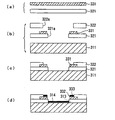
- FIG. 1 is a cross-sectional view of a metal substrate according to the first embodiment of the present invention.
- 2A to 2D are process cross-sectional views for explaining a metal substrate manufacturing process according to the first embodiment of the present invention.
- FIG. 3 is a cross-sectional view of a light source device using a metal substrate according to the first embodiment of the present invention.
- FIG. 4 is a cross-sectional view of a light source device using a metal substrate according to the first embodiment of the present invention.
- FIG. 5 is a cross-sectional view showing a preferred structure of the submount.
- FIG. 6 is a cross-sectional view of a light source device using a metal substrate according to the first embodiment of the present invention.
- FIG. 1 is a cross-sectional view of a metal substrate according to the first embodiment of the present invention.
- 2A to 2D are process cross-sectional views for explaining a metal substrate manufacturing process according to the first embodiment of the present invention.
- FIG. 3 is a cross-section
- FIG. 7 is a cross-sectional view of a metal substrate according to the second embodiment of the present invention.
- 8A to 8D are process cross-sectional views for explaining a metal substrate manufacturing process according to the second embodiment of the present invention.
- FIG. 9 is a cross-sectional view of a light source device using a metal substrate according to the second embodiment of the present invention.
- FIG. 10 is a cross-sectional view of a metal substrate according to the third embodiment of the present invention.
- FIGS. 11A to 11D are process cross-sectional views for explaining a metal substrate manufacturing process according to the third embodiment of the present invention.
- FIG. 12 is a cross-sectional view of a light source device using a metal substrate according to the third embodiment of the present invention.
- FIG. 13 is a cross-sectional view of a metal substrate according to a preferred embodiment of the present invention.
- FIG. 14 is a cross-sectional view of a metal substrate according to a preferred embodiment of the present invention.
- FIG. 15 is a cross-sectional view of a metal substrate according to a preferred embodiment of the present invention.
- FIG. 16 is a cross-sectional view of a metal substrate according to a preferred embodiment of the present invention.
- FIG. 17 is a cross-sectional view of a light source device using a metal substrate according to the first embodiment of the present invention.
- FIG. 18 is a cross-sectional view of a white light source device using a metal substrate according to the first embodiment of the present invention.
- FIG. 19 is a cross-sectional view of a white light source device using a metal substrate according to the first embodiment of the present invention.
- FIG. 20 is a graph showing the input power dependence of the total radiant flux of the light source devices of Example 2 and Comparative Example 2 (no phosphor dome).
- FIG. 21 is a graph showing the input power dependence of the total radiant flux normalized by the total area of the LED chips of the light source devices of Example 2 and Comparative Example 2 (without phosphor dome).
- FIG. 22 is a graph showing the dependence of the efficiency (total radiant flux per input power) of the light source device (without the phosphor dome) of Example 2 and Comparative Example 2 on the input power.
- FIG. 20 is a graph showing the input power dependence of the total radiant flux of the light source devices of Example 2 and Comparative Example 2 (no phosphor dome).
- FIG. 21 is a graph showing the input power dependence of the total radiant flux normalized by the total area of the LED chips of the light source devices of Example 2 and Comparative Example 2
- FIG. 23 is a graph showing the dependence of the efficiency (total radiant flux per input power) on the input power of the light source devices of Example 2 and Comparative Example 2 (without the phosphor dome) normalized by the total area of the LED chip. It is.
- FIG. 24 is a graph showing the input power dependence of the emission peak wavelength of the light source devices (without the phosphor dome) of Example 2 and Comparative Example 2.
- FIG. 25 is a graph showing the measurement results of the surface temperature of the LED chip when the input power is 11 W in the light source devices of Example 2 and Comparative Example 2 (no phosphor dome).
- FIG. 26 is a graph showing the dependence of the total luminous flux on the input power of the white light source device (with the phosphor dome) of Example 2 and Comparative Example 2.
- FIG. 24 is a graph showing the input power dependence of the emission peak wavelength of the light source devices (without the phosphor dome) of Example 2 and Comparative Example 2.
- FIG. 25 is a graph showing the measurement results of the surface temperature of the LED
- FIG. 27 is a graph showing the dependence of the total luminous flux input power on the white light source device (with phosphor dome) of Example 2 and Comparative Example 2 normalized by the total area of the LED chip.
- FIG. 28 is a graph showing dependency of the efficiency (total luminous flux per input power) of the white light source device (with the phosphor dome) of Example 2 and Comparative Example 2 on input power.
- FIG. 29 is a graph showing the dependence of the efficiency (total luminous flux per input power) on the input power dependence of the white light source device of Example 2 and Comparative Example 2 (with a phosphor dome) normalized by the total area of the LED chip. It is.
- FIG. 28 is a graph showing dependency of the efficiency (total luminous flux per input power) of the white light source device (with the phosphor dome) of Example 2 and Comparative Example 2 normalized by the total area of the LED chip.
- FIG. 30 is a graph showing the energization time dependency of the total luminous flux in the white light source device (with the phosphor dome) of Example 2 and Comparative Example 2 when the input power is 11 W.
- FIG. 31 is a graph showing the energization time dependency of the total luminous flux normalized by the total area of the LED chip when the input power is 11 W in the white light source device of Example 2 and Comparative Example 2 (with a phosphor dome). is there.
- FIG. 32 is a graph showing the dependence of the surface temperature of the fluorescent dome on the energization time of the white light source device (with the phosphor dome) of Example 2 and Comparative Example 2 when the input power is 11 W.
- FIG. 31 is a graph showing the energization time dependency of the total luminous flux normalized by the total area of the LED chip when the input power is 11 W in the white light source device of Example 2 and Comparative Example 2 (with a phosphor dome). is there.
- FIG. 32 is a graph showing
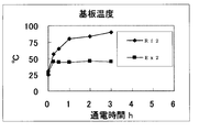
- FIG. 33 is a graph showing the dependence of the substrate temperature on the energization time when the input power is 11 W in the white light source device (with the phosphor dome) of Example 2 and Comparative Example 2.
- FIG. 34 is a graph showing the input power dependence of Ra (average color rendering index) of the white light source device (with phosphor dome) of Example 2 and Comparative Example 2.
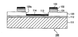
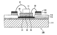
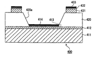
- the metal substrate 100 has an Al plate 111 having a Ni layer 112 laminated on the entire surface of one side as a heat radiating metal plate.
- a white film 120 made of an insulating resin is laminated on a part of the Ni layer 112.
- a wiring pattern made of Cu foil 131 is formed on the white film 120.
- a Ni layer 132 and an Au layer 133 are laminated in this order.
- the white film 120 has a through hole 120 a in a part thereof, and an Au layer 114 is laminated on the Ni layer 112 exposed at the position of the through hole via the Ni layer 113.
- the surface of the Au layer 114 is a light source mounting surface.
- a manufacturing process of the metal substrate 100 will be described with reference to FIGS. First, as shown to Fig.2 (a), Cu foil 131 is laminated
- the Cu foil 131 is etched to form a wiring pattern, and a part of the white film 120 is punched using a punching die such as a big die to form a through hole 120a. To do.
- a Ni layer 112 is previously laminated on the entire surface of one side as a heat dissipation metal plate on the surface of the white film 120 opposite to the surface on which the wiring pattern (Cu foil 131) is formed.
- the laminated Al plate 111 is laminated by a vacuum press.
- the thickness of the Al plate 111 can be set to 0.1 mm to 5 mm, for example. In practice, the Al plate 111 having a thickness that provides the required strength is selected in consideration of the size of the metal substrate 100 to be manufactured.
- the Ni layer 112 is formed by an electroless plating process.
- the surface of the Al plate 111 is etched with an alkali or the like, and further subjected to an acid treatment with nitric acid or the like, followed by zinc substitution with an alkaline zinc substitution solution.
- the thickness of the Ni layer 112 can be 0.1 ⁇ m to 10 ⁇ m.
- the Ni layer 112 can also be formed by a dry method such as a vacuum evaporation method or a sputtering method, in which case the zinc replacement treatment is not necessary.
- the wet plating process is more suitable for mass production than the dry process because a large number of Al plates 111 can be processed at once.
- a Ni layer 113 and an Au layer 114 are formed in this order on the surface of the Ni layer 112 exposed through the through-hole 120a of the white film by using an electroless plating technique.
- the Ni layer 132 and the Au layer 133 are also formed on the surface of the Cu foil 131 constituting the wiring pattern.
- the thickness of the Ni layer 132 formed in this step is preferably 2 ⁇ m to 8 ⁇ m.
- the thickness of the Au layer can be 0.01 ⁇ m to 10 ⁇ m, but is preferably 0.1 ⁇ m or more in order to improve the wire bonding property of the Au layer 133 formed on the Cu foil 131.
- the thickness of the Au layer formed in this step is preferably 2 ⁇ m or less, more preferably 1 ⁇ m or less.
- the metal substrate 100 does not have a portion where the white film 120 is laminated on the Au layer 114, and the entire lower surface thereof is in contact with the Ni layer 112. Therefore, the white film 120 hardly peels off. Moreover, since the Au layer is formed only in the area where the LED chip is mounted except on the wiring pattern, the amount of expensive Au used is reduced.
- the use of Au in a light source device that includes a short-wavelength visible light component in the output light reduces luminous efficiency. There is a case to let you.
- the use of Au is limited to the light source mounting surface, and further, the surface of the metal plate other than the light source mounting surface is covered with the white film 120, so We are trying to improve.
- the Ni plating process is performed twice on the Al plate 111 before the Au layer 114 is formed, there are two Ni layers 112 and 113 between the Al plate 111 and the Au layer 114. It is separated. Therefore, harmful alloying reaction that occurs when Al and Au come into contact with each other is reliably prevented.
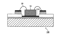
- FIG. 3 shows a cross-sectional view of a light source device configured using the metal substrate 100.
- the LED chip 10 is fixed to the surface of the Au layer 114 serving as a light source mounting surface by using a brazing material (not shown) such as Au—Sn solder, and a wiring pattern (Cu foil 131) is further formed by bonding wires 20. ) To obtain. Since the light source mounting surface is made of Au having good solder wettability, the LED chip 10 and the light source mounting surface are firmly coupled.
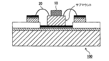
- the submount When mounting the LED chip on the metal substrate 100, it is also possible to use a submount as shown in FIG.
- the use of the submount is particularly effective when a vertical electrode type LED chip having a semiconductor light emitting element structure formed on a conductive substrate made of a semiconductor or metal is mounted.
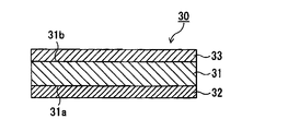
- a submant having a very simple structure as shown in FIG. 5 can be preferably used.
- the submount 30 shown in FIG. 5 has metallized layers 32 and 33 on main surfaces 31a and 31b of a ceramic plate 31 made of AlN, alumina, or the like.
- the thickness of the ceramic plate 31 is preferably 0.1 mm to 0.5 mm, and the thickness of the metallized layers 32 and 33 is preferably 0.1 ⁇ m to 10 ⁇ m.
- the outermost layer is formed of a metal having good solder wettability. Further, it is desirable that at least one of the metallized layers 32 and 33 is made of a metal excellent in both solder wettability and wire bonding property, for example, Au, and the outermost layer is formed.
- a preferable metallized layer whose outermost layer is an Au layer is, for example, a multilayer film having a laminated structure of Ti / Pt / Au, Ti / Ni / Au, Cr / Au, Ti / Au, etc. in order from the side in contact with the ceramic plate. is there.
- the thickness of the Au layer is preferably 0.1 ⁇ m or more, more preferably 0.3 ⁇ m or more, and particularly preferably 0.5 ⁇ m or more. Since forming a thick Au layer causes an increase in cost, the thickness of the Au layer is preferably 2 ⁇ m or less, more preferably 1 ⁇ m or less.
- FIG. 6 shows a cross-sectional view of a light source device in which the vertical electrode type LED chip 11 having a conductive substrate is mounted on the metal substrate 100 using the submount 30 described above.
- solder (not shown) is provided between the Au layer 114 providing the light source mounting surface and the submount 30 (metallized layer 32), and between the submount 30 (metalized layer 33) and the LED chip 11. Connected).
- the electrode on the upper surface side of the LED chip 11 is connected to one wiring pattern by a bonding wire 21.
- the electrode on the lower surface side of the LED chip 11 is connected to the other wiring pattern via the metallized layer 33 and the bonding wire 22.
- the Al substrate 111 and the LED chip 11 are insulated by a ceramic plate 31 included in the submount 30.
- the vertical electrode type LED chip 11 is disclosed in, for example, US Patent Publication No. 2006/0154389, an LED chip having a metal substrate as a support substrate in the chip, and disclosed in Japanese Patent Application Laid-Open No. 2006-179511.
- a horizontal electrode type LED chip using a conductive substrate and taking out light from the chip surface on the side where the positive and negative electrodes are provided is mounted on the metal substrate 100, the above-mentioned sub The mount 30 can be preferably used.
- Such an LED chip is described in, for example, International Publication No.
- the ceramic substrate 31 insulates the conductive substrate of the LED chip from the heat-dissipating metal plate of the metal substrate, so that leakage can be prevented and a plurality of LED chips can be mounted on one metal substrate. In the case of mounting, the degree of freedom of interchip wiring is increased.
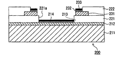
- FIG. 7 shows a cross-sectional view of the metal substrate according to the second embodiment.
- the metal substrate 200 has an Al plate 211 having a Ni layer 212 laminated on the entire surface of one side as a heat radiating metal plate. A part of the Ni layer 212 is laminated with a first white film 221 made of an insulating resin. On the first white film 221, a wiring pattern made of Cu foil 231 is formed, and a second white film 222 made of an insulating resin is laminated so as to expose a part of the wiring pattern. .
- a Ni layer 232 and an Au layer 233 are laminated in this order on the surface exposed to a part of the Cu foil 231.
- the first white film 221 and the second white film 222 respectively have through holes 221a and 222a in a part thereof, and the Ni layer 213 is formed on the Ni layer 212 exposed at the positions of these through holes.
- the Au layer 214 is laminated via The surface of the Au layer 214 is a light source mounting surface.
- a manufacturing process of the metal substrate 200 will be described with reference to FIGS. First, as shown to Fig.8 (a), Cu foil 231 is laminated
- the Cu foil 231 is etched to form a wiring pattern, and a part of the first white film 221 is punched out using a big die, so that the first through hole 221a is formed.
- a second white film 222 made of the same insulating resin material as the first white film 221 is prepared.
- a second through hole 222a is formed by punching using a big die.
- the second white film 222 serves as a protective layer for protecting the wiring pattern (Cu foil 231) formed on the first white film 221.
- the through hole 222a (50) of the second white film 222 is part of the wiring pattern made of the Cu foil 231 so that the through hole 221a of the first white film 221 is accommodated inside the through hole 222a (50).
- the shape and size are set so that (the part forming the wire bonding terminal) is exposed.
- Ni layer 212 was previously laminated
- the Al plate 211 is laminated by a vacuum press. In this vacuum pressing step, the second white film 222 is laminated on the first white film 221 at the same time.
- an electroless plating technique is used on the surface of the Ni layer 212 exposed through the through hole 221a of the first white film 221 and the through hole 222a of the second white film 222. Then, the Ni layer 213 and the Au layer 214 are formed in this order. At the same time, the Ni layer 232 and the Au layer 233 are also formed on the partially exposed surface of the wiring pattern (Cu foil 231).
- the preferable thicknesses of the Al plate, Ni layer, and Au layer in the metal substrate 200 refer to the preferable thicknesses of the corresponding structures in the metal substrate 100 according to the first embodiment.
- FIG. 9 shows a cross-sectional view of a light source device configured using the metal substrate 200.
- the LED chip 10 is fixed to the surface of the Au layer 214 as a light source mounting surface by using a brazing material (not shown) such as Au—Sn solder, and further connected to the wiring pattern by the bonding wires 20. Is obtained. Since the light source mounting surface is made of Au with good solder wettability, the LED chip and the light source mounting surface are strongly bonded.
- the above-described submount 30 can be preferably used.
- FIG. 3 A cross-sectional view of a metal substrate according to the third embodiment is shown in FIG.
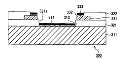
- the metal substrate 300 has a Cu plate 311 as a heat radiating metal plate.
- a first white film 321 made of an insulating resin is laminated on a part of the Cu plate 311.
- a wiring pattern made of Cu foil 331 is formed on the first white film 321 and a second white film 322 made of an insulating resin is exposed so that a part of the wiring pattern (Cu foil 331) is exposed.
- a Ni layer 332 and an Au layer 333 are laminated in this order.
- the first white film 321 and the second white film 322 each have through holes 321a and 322a in a part thereof, and a Ni layer 313 is formed on the surface of the Cu plate 311 exposed at the positions of these through holes.
- An Au layer 314 is laminated via The surface of the Au layer 314 is a light source mounting surface.
- a manufacturing process of the metal substrate 300 will be described with reference to FIGS. First, as shown to Fig.11 (a), Cu foil 331 is laminated
- the Cu foil 331 is etched to form a wiring pattern, and a part of the first white film is punched out using a big die, and the first through hole 321a is formed.
- a second white film 322 made of the same insulating resin material as the first white film 321 is prepared.
- a second through hole 322a is formed by punching using a big die.
- the second white film 322 serves as a protective layer for protecting the wiring pattern (Cu foil 331) formed on the first white film 321.
- the through hole 322a of the second white film 322 is formed so that the through hole 321a of the first white film is accommodated inside thereof, and a part of the wiring pattern (Cu foil 331) (wire bonding terminal) The shape and size are set so that the portion that forms) is exposed.
- a Cu plate 311 is laminated on the surface of the first white film 321 opposite to the surface on which the wiring pattern (Cu foil 331) is formed by a vacuum press.
- the second white film 322 is also laminated on the first white film 321 at the same time.
- the surface of the Cu plate 311 exposed through the through hole 321a of the first white film and the through hole 322a of the second white film is subjected to Ni using an electroless plating technique.
- a layer 313 and an Au layer 314 are formed in this order.
- the Ni layer 332 and the Au layer 333 are also formed on the partially exposed surface of the wiring pattern (Cu foil 331).
- the Ni layer 313 functions as a barrier layer that prevents Cu from diffusing from the Cu plate 311 to the Au layer 314.
- the diffusion of Cu reduces the solder wettability of the Au layer surface.
- the preferable thicknesses of the Cu plate, the Ni layer, and the Au layer in the metal substrate 300 refer to the preferable thicknesses of the corresponding structures in the metal substrate 100 according to the first embodiment.
- the first white film 321 does not have a portion laminated on the Au layer 314, and the entire lower surface thereof is in contact with the Cu plate 311, so that the first white film 321 is peeled off. hard.
- the first white film 321 can be laminated on the Ni layer after the Ni layer is laminated on the entire surface of the Cu plate 311 on which the light source mounting surface is formed.
- FIG. 12 is a cross-sectional view of a light source device configured using a metal substrate 300 according to the third embodiment.
- the LED chip 10 is fixed to the surface of the Au layer 314 as a light source mounting surface using a brazing material (not shown) such as Au—Sn solder, and further connected to the wiring pattern by the bonding wires 20. Is obtained. Since the light source mounting surface is made of Au with good solder wettability, the LED chip and the light source mounting surface are strongly bonded.
- the LED chip includes a conductive substrate, and the LED chip is fixed so that the conductive substrate faces the light source mounting surface, the above-described submount 30 may be used.
- the wiring board made of the white film and the patterned Cu foil can have a multilayer structure (multilayer wiring board) as necessary.
- the method of forming a through-hole in a white film is not limited to the method using the above-mentioned big type, and for example, a method using laser processing or router processing may be used.
- FIGS. 2, 8 and 11 used to describe the manufacturing process of the metal substrate according to each of the above embodiments, only one metal substrate is drawn, but this is for convenience only.
- a method in which a large number of metal substrates are collectively formed using a large-area heat-dissipating metal plate and then cut is suitable.
- the LED chip that can be mounted on the metal substrate according to each of the above embodiments is not limited, and a red LED chip using an AlGaAs semiconductor, a yellow LED chip using an AlGaInP semiconductor, and a green LED using a GaP semiconductor.
- Various LED chips such as a chip, a green to blue LED chip using a ZnSe semiconductor, a green to ultraviolet LED chip using an AlGaInN semiconductor, and a blue to ultraviolet LED chip using a ZnO semiconductor can be mounted.
- the size of the light source mounting surface can be appropriately set according to the size and number of LED chips to be mounted.
- a preferable bonding material used for bonding the light source mounting surface and the LED chip is solder (brazing material).
- the surface of the LED chip can also be metallized as necessary so that the bonding by solder is performed firmly.
- the LED chip fixed on the light source mounting surface can be sealed with a transparent resin or glass.
- a known technique may be referred to for a preferable sealing material, one of the most preferable sealing materials is a silicone resin. The reason is that it is excellent in transparency and light resistance in the visible wavelength region.
- the molding method of the sealing material and a method usually used in the field such as potting molding and molding can be arbitrarily used.
- Each of the metal substrates according to the above embodiments has a cavity on the light source mounting surface side. That is, it is a cavity having the surface of the through hole provided in the white film as a side wall and the light source mounting surface as a bottom surface. The depth of the cavity can be adjusted by changing the thickness of the white film.
- the side wall of the cavity is such that the light emitted from the LED chip fixed on the light source mounting surface is reflected by the side wall of the cavity and guided in the opening direction of the cavity. Can be tilted.
- the cross-sectional area may be changed in the film thickness direction of the film.
- a cross-sectional area here is an area of a cross section formed by cutting through-holes in a plane orthogonal to the thickness direction of the white film.
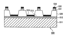
- the heat radiating metal plate as the base material is superior in rigidity, thermal stability, etc. compared to the resin plate, and unlike the ceramic plate, it has a property that is difficult to break. It is also possible to form a large area so as to exceed. In the case of increasing the area, it is preferable to provide a plurality of the cavities as in the metal substrate 500 shown in FIG.
- the feature of the metal substrate of the present invention that the white film is difficult to peel from the heat-dissipating metal plate is advantageous for manufacturing a large-area product.
- the metal substrate according to the present invention may include a cavity formed by processing a heat radiating metal plate.
- FIG. 15 is a cross-sectional view showing an example of such a metal substrate.
- the metal substrate 600 includes an Al plate 611 having a Ni layer 612 laminated on the entire surface of one side as a heat radiating metal plate.
- the heat radiating metal plate is formed with a protruding portion protruding to the Ni layer 612 side by pressing.
- the convex portion has a ring shape in plan view.
- the through hole formed in the white film 620 is formed in a circular shape having a diameter larger than the outer diameter of the ring-shaped convex portion.
- the Ni layer 613 and the Au layer 614 formed by the electroless plating method also cover the surface of the ring-shaped convex portion.
- the inside of the ring-shaped convex portion protruding into the light source mounting surface is a cavity.
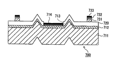
- FIG. 16 is a cross-sectional view showing another example of a metal substrate having a cavity formed by processing a heat radiating metal plate.
- the metal substrate 700 includes an Al substrate 711 having a Ni layer 712 laminated on the entire surface of one side as a heat radiating metal plate.
- the heat radiating metal plate is formed with a protruding portion protruding to the Ni layer 712 side by pressing.
- the convex portion has a ring shape in plan view.
- the white film 720 is formed with a through-hole having a size that fits inside the ring-shaped convex portion.
- the Ni layer 713 and the Au layer 714 are formed by electroless plating, whereby the light source mounting surface (Au layer 714) is formed inside the ring-shaped convex portion (in the cavity). Surface). Since the surface of the ring-shaped convex part is covered with the white film 720, it has high light reflectivity.
- Y 2 SiO 5 : Ce, Tb means “Y 2 SiO 5 : Ce”, “Y 2 SiO 5 : Tb”, and “Y 2 SiO 5 : Ce, Tb”.
- (La, Y) 2 O 2 S: Eu” means “La 2 O 2 S: Eu”, “La x Y 2 ⁇ x O 2 S: Eu” (0 ⁇ x ⁇ 2) ”and a general term including“ Y 2 O 2 S: Eu ”.
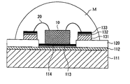
- the light source device whose sectional view is shown in FIG.
- This light source device can be a white light source device by dispersing a yellow phosphor such as YAG: Ce in the resin mold M. Further, when a red phosphor such as (Mg, Ca, Sr, Ba) AlSiN 3 : Eu is used in addition to the yellow phosphor, a white light source device having a lower color temperature can be obtained.
- a part or all of the yellow phosphor is replaced with (Ba, Ca, Sr, Mg) 2 SiO 4 : Eu, Eu-activated ⁇ sialon, (Ba, Sr, Ca). It may be replaced with a green phosphor such as 3 Si 6 O 12 N 2 : Eu.
- the phosphor can be applied to the surface of the blue LED chip 10 using a silicone resin as a binder.
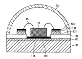
- the phosphor dome RD is formed by forming a translucent composition in which a phosphor is dispersed in a transparent resin into a dome shape.
- the phosphor added to the phosphor dome is the same as the phosphor dispersed in the resin mold in the above example.
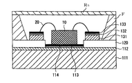
- the phosphor sheet RS is obtained by forming a translucent composition in which a phosphor is dispersed in a transparent resin into a sheet shape.
- the phosphor added to the phosphor sheet RS is the same as the phosphor dispersed in the resin mold in the above example.
- the phosphor dome or the phosphor sheet is disposed at a position spatially separated from the blue LED chip. That is, since the phosphor is disposed at a position spatially separated from the light source mounting surface of the metal substrate and the LED chip with the gap interposed therebetween, the heat insulating effect by the gap causes the phosphor generated by heat generated in the LED chip. Temperature rise is suppressed. As a result, a decrease in efficiency and deterioration of the phosphor due to heat are suppressed. Furthermore, in the example of FIG. 18 in which the phosphor-containing layer is formed in a dome shape, the energy density of excitation light received by the phosphor is lower than in the example of FIG.
- blue phosphor examples include BaMgAl 10 O 17 : Eu, (Sr, Ba, Ca) 5 (PO 4 ) 3 Cl: Eu, and the like.
- Examples include O 12 : Ce, CaSc 2 O 4 : Ce, BaMgAl 10 O 17 : Eu, Mn, and the like.
- yellow phosphors examples include phosphors activated with Ce, such as YAG: Ce, TAG: Ce, La 3 Si 6 N 11 : Ce, and SiAlON type oxynitride fluorescence activated with Eu.
- the body Ca x (Si, Al) 12 (O, N) 16 : Eu or the like can also be used.
- the white film made of insulating resin used in the metal substrate according to each of the above embodiments is composed of a resin composition obtained by mixing a white pigment with a thermoplastic resin or a thermosetting resin as a base resin. .
- a white film when a white film is used as an insulating plate of a wiring board, especially when a wire bonding terminal is formed on the wiring pattern, wire bonding is possible.
- the white film needs to be hard.
- examples of the thermosetting resin include a phenol resin, an epoxy resin, and a polyimide resin.
- a thermoplastic resin the high heat resistant thermoplastic resin mentioned later is mentioned.
- thermosetting resin-based white film is obtained by applying an uncured white resin composition to the surface of the heat radiating metal plate instead of laminating a pre-formed film on the heat radiating metal plate. It can also be formed by a method of heat curing.
- thermoplastic resin material suitable for a white film that also functions as an insulating plate of a wiring board for example, polyether ether ketone (PEEK), polyether ketone (PEK), polyphenylene sulfide (PPS), polyether sulfone (PES) ), Polyphenylene ether (PPE), polyamideimide (PAI), polyetherimide (PEI), polyphenylsulfone (PPSU), and liquid crystal polymer (LCP).
- PEEK polyether ether ketone
- PEK polyether ketone
- PPS polyphenylene sulfide
- PES polyether sulfone
- PPE polyamideimide
- PAI polyetherimide
- PESU polyphenylsulfone
- LCP liquid crystal polymer
- any one or more selected from liquid crystal polymers any one or more selected from a crystalline thermoplastic resin having a crystal melting peak temperature (Tm) of 260 ° C. or higher and an amorphous thermoplastic resin having a glass transition temperature (Tg) of 260 ° C. or higher is selected. It is more preferable to use it.
- Tm crystal melting peak temperature
- Tg glass transition temperature
- the reflow temperature becomes as high as 300 ° C. or higher, so a crystalline thermoplastic resin having a crystal melting peak temperature of 300 ° C. or higher, and a glass transition temperature of 300 ° C. It is more preferable to use at least one selected from the above amorphous thermoplastic resins and liquid crystal polymers having a liquid crystal transition temperature of 300 ° C. or higher. Crystalline thermoplastic resins having a crystal melting peak temperature of 260 ° C.
- PAI polyamideimide
- the above exemplified crystalline thermoplastic resins may be used singly or as a mixed resin composition in which a plurality of types are mixed. Further, this crystalline thermoplastic resin may be used as a mixed resin composition in which an amorphous thermoplastic resin such as polyetherimide (PEI) is mixed.
- PEI polyetherimide
- a resin composition comprising a crystalline polyaryl ketone resin (A) having a crystal melting peak temperature of 260 ° C. or higher and 80 to 20% by weight and an amorphous polyetherimide resin (B) of 20 to 80% by weight.
- the white film used for the base resin has excellent adhesion between the films, as well as adhesion to the metal plate and metal foil, as well as necessary for manufacturing a substrate with a wiring pattern protection layer or a multilayer wiring substrate.
- Pb-free solder has excellent heat resistance and hardly discolors even in the reflow process.
- the resin composition comprising the crystalline polyaryl ketone resin (A) and the amorphous polyetherimide resin (B) preferably has a polyaryl ketone resin (A) content of from the viewpoint of increasing heat resistance. Is 20% by weight or more, more preferably 30% by weight or more, and still more preferably 40% by weight or more.
- the content of the polyaryl ketone resin (A) in this resin composition is preferably 80% by weight or less, more preferably 75% by weight or less, and still more preferably 70% by weight or less.
- the crystalline polyaryl ketone resin (A) is a thermoplastic resin having an aromatic nucleus bond, an ether bond and a ketone bond in its structural unit. Specific examples thereof include polyether ketone (glass transition temperature [hereinafter referred to as “Tg”]: 157 ° C., crystal melting peak temperature (hereinafter referred to as “Tm”]: 373 ° C.), polyether ether ketone (Tg: 143 C, Tm: 334 ° C.), polyether ether ketone ketone (Tg: 153 ° C., Tm: 370 ° C.), and the like. Among them, those having a Tm of 260 ° C. or higher, particularly 300 to 380 ° C. are preferable from the viewpoint of heat resistance.
- the crystalline polyaryl ketone resin (A) may contain a biphenyl structure, a sulfonyl group, or other repeating units as long as the effects of the present invention are not impaired
- polyaryl ketone resins mainly composed of polyether ether ketone having a repeating unit represented by the following structural formula (1).
- the main component means that the content exceeds 50% by weight.
- polyether ether ketones are trade names “PEEK151G” (Tg: 143 ° C., Tm: 334 ° C.), “PEEK381G” (Tg: 143 ° C., Tm: 334 ° C.), “PEEK450G” manufactured by VICTREX. (Tg: 143 ° C., Tm: 334 ° C.) and the like.
- Two or more types of polyaryl ketone resins corresponding to the polyaryl ketone resin (A) can also be used in combination.
- amorphous polyetherimide resin (B) examples include amorphous polyetherimide resins having a repeating unit represented by the following structural formula (2) or (3).
- An amorphous polyetherimide resin having a repeating unit represented by the structural formula (2) or (3) is 4,4 ′-[isopropylidenebis (p-phenyleneoxy)] diphthalic dianhydride and p- As a polycondensate with phenylenediamine or m-phenylenediamine, it can be produced by a known method.
- Commercially available products of these non-crystalline polyetherimide resins include “Ultem 1000” (Tg: 216 ° C.), “Ultem 1010” (Tg: 216 ° C.) or “Ultem CRS 5001” (Tg 226) manufactured by General Electric. ° C) and the like.
- an amorphous polyetherimide resin having a repeating unit represented by the structural formula (2) is particularly preferable.
- two or more types of polyetherimide resins corresponding to the polyetherimide resin (B) can be used in combination.
- the preferable thermoplastic resin material is used for forming a white film as a composition to which an inorganic filler is added.
- the inorganic filler include talc, mica, mica, glass flake, boron nitride (BN), calcium carbonate, aluminum hydroxide, silica, titanate (potassium titanate, etc.), barium sulfate, alumina, kaolin, clay , Titanium oxide, zinc oxide, zinc sulfide, lead titanate, zirconium oxide, antimony oxide, magnesium oxide and the like. These may be added singly or in combination of two or more.
- These inorganic fillers are preferably treated with a silane coupling agent on the surface in order to improve dispersibility.
- the white film preferably has an average reflectance of 70% or more at a wavelength of 400 to 800 nm by addition of the inorganic filler. Further, considering that a blue LED chip is generally used as an excitation light source of the white light source device, the white film preferably has a high reflectance near 470 nm corresponding to the emission wavelength of the blue LED chip. Specifically, the reflectance at 470 nm is preferably 70% or more, and more preferably 75% or more.
- a resin composition having a thermoplastic resin as a base resin can be formed into a film by, for example, an extrusion casting method using a T-die or a calendar method.
- the molding temperature in the extrusion casting method using a T die is appropriately adjusted depending on the flow characteristics or film formability of the composition, but is generally about the melting point or higher and 430 ° C. or lower.
- a crystallization treatment method for imparting heat resistance includes a method of crystallizing at the time of extrusion casting (cast crystallization method), a heat treatment roll or a hot air oven in a film forming line, etc. And a method of crystallizing by using a hot air furnace or a hot press outside the film forming line (outline crystallization method).
- the average of the linear expansion coefficients of the MD and TD is preferably not more than 35 ⁇ 10 ⁇ 6 / ° C.
- the linear expansion coefficient exceeds 35 ⁇ 10 ⁇ 6 / ° C., curling tends to occur when a metal foil for wiring patterns is laminated.
- the preferred range of linear expansion coefficient varies depending on the type of metal foil used or the wiring pattern formed on the surface, but is generally about 10 ⁇ 10 ⁇ 6 to 30 ⁇ 10 ⁇ 6 / ° C.
- the difference in linear expansion coefficient between MD and TD is preferably 20 ⁇ 10 ⁇ 6 / ° C. or less, more preferably 15 ⁇ 10 ⁇ 6 / ° C. or less, and even more preferably 10 ⁇ 10 ⁇ 6 / ° C. Most preferably: By reducing the anisotropy in this way, the problem of curling in the direction where the linear expansion coefficient is large is reduced.
- a resin composition comprising 80 to 20% by weight of the crystalline polyaryl ketone resin (A) having a crystal melting peak temperature of 260 ° C. or higher, with the balance being an amorphous polyetherimide resin (B),
- A crystalline polyaryl ketone resin
- B amorphous polyetherimide resin
- the filler 1 having an average particle size of 15 ⁇ m or less and an average aspect ratio (average particle size / average thickness) of 30 or more and a filler 2 having a large refractive index difference (generally a filler) 2 to 100 parts by weight of an inorganic filler containing at least a refractive index of 1.6).
- a filler 2 having a large refractive index difference (generally a filler) 2 to 100 parts by weight of an inorganic filler containing at least a refractive index of 1.6.
- the amount of the inorganic filler is less than 25 parts by weight, it becomes difficult to balance the reflectance and the linear expansion coefficient.
- the inorganic filler is poorly dispersible or breaks when the white film is formed. This causes a problem in formability.
- the filler 1 and the filler 2 having the physical property values specified above as the inorganic filler it has a good reflectance and at the same time has no anisotropy in the linear expansion coefficient. A white film excellent in
- Examples of the filler 1 having an average particle size of 15 ⁇ m or less and an average aspect ratio (average particle size / average thickness) of 30 or more are, for example, synthetic mica, natural mica (mascobite, phlogopite, sericite, szolite, etc.), fired.
- Examples thereof include inorganic scale-like (plate-like) fillers such as natural or synthetic mica, boehmite, talc, illite, kaolinite, montmorillonite, vermiculite, smectite, and plate-like alumina, and scale-like titanates.
- the said filler By using these fillers, the difference in the linear expansion coefficient between the MD (film flow direction) and TD (direction orthogonal to the flow direction) of the white film can be suppressed.
- scaly titanate is preferable because of its high refractive index.
- the said filler can be used individually or in combination of 2 or more types.
- the content of the filler 1 is preferably 10 parts by weight or more with respect to 100 parts by weight of the resin composition, more preferably 20 parts by weight or more, and most preferably 30 parts by weight or more. preferable.
- the filler 2 is an inorganic filler having a large refractive index difference from the resin. That is, the inorganic filler has a large refractive index.
- the inorganic filler has a large refractive index.
- calcium carbonate, barium sulfate, zinc oxide, titanium oxide, titanate, or the like having a refractive index of 1.6 or more is preferably used, and titanium oxide is particularly preferably used.
- Titanium oxide has a significantly higher refractive index (approximately 2.50 or more) than other inorganic fillers, and can increase the difference in refractive index from the base resin. Therefore, when other fillers are used Therefore, excellent reflectivity can be obtained with a smaller amount. Even if the film thickness is reduced, a white film having high reflectivity can be obtained.
- the titanium oxide is preferably a crystalline type such as anatase type or rutile type, and among them, rutile type titanium oxide is preferable because of a large difference in refractive index from the base resin.
- rutile type titanium oxide is preferable because of a large difference in refractive index from the base resin.
- the titanium oxide manufactured by the chlorine method is preferable from the point of whiteness.
- the inert inorganic oxide include silica, alumina, and zirconia.
- titanium oxide whose surface is treated with a silane coupling agent in order to enhance dispersibility.
- the particle size of titanium oxide is preferably 0.1 ⁇ m or more, more preferably 0.2 ⁇ m or more. Moreover, it is preferable that it is 1.0 micrometer or less, More preferably, it is 0.5 micrometer or less.
- the content of titanium oxide is preferably 15 parts by weight or more with respect to 100 parts by weight of the base resin composed of the crystalline polyaryl ketone resin (A) and the amorphous polyetherimide resin (B).
- the amount is more preferably 20 parts by weight or more, and most preferably 25 parts by weight or more.
- Additives having various purposes such as heat stabilizers, ultraviolet absorbers, light stabilizers, nucleating agents, colorants, lubricants, flame retardants, etc., to the extent that the properties of the resin composition constituting the white film are not impaired. May be appropriately blended.
- a well-known method can be used.
- a masterbatch in which various additives are mixed with an appropriate base resin at a high concentration (typically 10 to 60% by weight) is prepared, and a base is used.
- a method of adjusting the concentration to the resin and mixing it is preferable from the viewpoint of the dispersibility of the additive and the workability during the production.
- the white film preferably has a reflectance reduction rate at a wavelength of 470 nm after heat treatment at 200 ° C. for 4 hours of 10% or less, and in particular, the reflectance reduction rate at a wavelength of 470 nm after heat treatment at 260 ° C. for 5 minutes. Is preferably 10% or less.
- the manufacturing process of the light source device using the metal substrate according to the present invention includes a thermosetting process (100 to 200 ° C., several hours) of a sealing agent such as an epoxy resin and a silicone resin, and a soldering process (Pb This is because there is a high possibility that free solder reflow, a peak temperature of 260 ° C., and a few minutes) will be included.
- the reduction rate of reflectance at a wavelength of 470 nm under the above heating test conditions is 10% or less, the reflectance of the white film resulting from these steps And a decrease in efficiency of the light source device due to this can be suppressed. Moreover, it becomes possible to suppress the reflectance fall of the white film resulting from the heat_generation
- the reduction rate of the reflectance at a wavelength of 470 nm under the above heating test conditions is more preferably 5% or less, further preferably 3% or less, and particularly preferably 2% or less.
- the resin composition comprising 80 to 20% by weight of the crystalline polyaryl ketone resin (A) having a crystal melting peak temperature of 260 ° C. or higher, with the balance being an amorphous polyetherimide resin (B).
- A crystalline polyaryl ketone resin
- B amorphous polyetherimide resin
- a metal foil having a thickness of about 5 ⁇ m to 70 ⁇ m made of, for example, copper, gold, silver, aluminum, nickel, tin or the like is used. it can.
- the method for laminating the metal foil on the white film is preferably a heat-sealing method that does not involve an adhesive layer, and is not limited, but is not limited to a hot press method, a heat laminating roll method, and a cast roll on an extruded resin.
- Preferred examples include an extrusion laminating method in which metal foils are laminated, or a method combining these.
- a protective layer can be produced from the same resin composition as the white film used for the insulating plate. Further, the protective layer may be formed using a thermosetting resin (epoxy resin, acrylic resin, polyimide resin, silicone resin, etc.) composition containing a white pigment such as titanium oxide.
- a preferable white pigment added to the composition includes the filler 1 having an average particle diameter of 15 ⁇ m or less and an average aspect ratio (average particle diameter / average thickness) of 30 or more.
- the resin composition comprising 80 to 20% by weight of the crystalline polyaryl ketone resin (A) having a crystal melting peak temperature of 260 ° C. or higher, with the balance being an amorphous polyetherimide resin (B).
- A crystalline polyaryl ketone resin
- B amorphous polyetherimide resin
- Example 1 In Example 1 and Comparative Example 1 described below, various measured values were obtained as follows.
- Crystal melting peak temperature (Tm) Using a differential scanning calorimeter “DSC-7” (manufactured by PerkinElmer), the temperature was determined from a thermograph according to JIS K7121, when 10 mg of a sample was heated at a heating rate of 10 ° C./min.
- Thermoplastic resin composition obtained by mixing 30 parts by weight of titanium oxide (average particle diameter 0.23 ⁇ m, alumina treatment, silane coupling agent treatment), 21 parts by weight of synthetic mica having an average particle diameter of 5 ⁇ m and an average aspect ratio of 50
- the product was melt-kneaded and extruded at a set temperature of 380 ° C. using an extruder equipped with a T-die to produce a white film having a thickness of 50 ⁇ m.
- the same resin composition was extruded at a set temperature of 380 ° C. using an extruder equipped with a T die, and at the same time, a copper foil (thickness: 35 ⁇ m) was laminated from one side to obtain a resin thickness of 50 ⁇ m and a copper foil thickness of 35 ⁇ m.
- a single-sided copper foil film was prepared. Then, while etching the single-sided copper foil film to form a wiring pattern, a through-hole was formed using a big die. Moreover, the through-hole was formed also in the white film using the big shape.
- a 1 mm thick Al plate (5052P) was preliminarily treated with zinc, and then a heat radiating metal plate with Ni plating was prepared.
- the above-mentioned white film (protective layer), single-sided copper foil film, and heat-dissipating metal plate were collectively laminated with a vacuum press machine under press conditions of 260 ° C. and 5 MPa for 30 minutes. After that, Ni plating treatment and Au plating treatment were sequentially performed on the surface of the heat radiation metal plate exposed at the wiring pattern portion and the through hole portion of the wiring substrate to produce a metal substrate. Further, by performing metal diffusion bonding under a reflow condition at 300 ° C. using an AuSn paste, an LED chip was fixed to the surface of the Au layer formed by the Au plating process, and a light source device was manufactured.
- the average reflectance (400 nm to 800 nm) of the produced white film is 80%, the reflectance at 470 nm before the heat treatment is 77%, and after the heat treatment (200 ° C. for 4 hours, 260 ° C. for 5 minutes). ) was 76%.
- the linear expansion coefficient was 25 ppm / ° C. for MD, 35 ppm / ° C. for TD, and the average of MD and TD was 30 ppm / ° C.
- Example 1 Similarly to Example 1, a white film having a thickness of 50 ⁇ m and a single-sided copper foil film having a resin thickness of 50 ⁇ m and a copper foil thickness of 35 ⁇ m were prepared. Thereafter, the single-sided copper foil film was etched to form a wiring pattern. In addition, the through-hole was not formed in the single-sided copper foil film.
- the white film (protective layer), the single-sided copper foil film, and the Al plate were laminated together in a vacuum press machine under the pressing conditions of 260 ° C., 5 MPa, and 30 minutes. Thereafter, an Ni plating process and an Au plating process were sequentially performed on the wiring pattern portion to produce an insulating aluminum substrate. Furthermore, the ceramic package on which the LED chip was mounted was mounted on the wiring pattern portion on the insulating layer using a solder paste, and a light source device was manufactured.
- Ni plating treatment and Au plating are further applied to a part of the Ni plating layer of an Al plate (heat radiating metal plate) having a Ni plating layer formed on the entire surface of one side and having a length and width of 20 mm ⁇ 20 mm and a thickness of 1 mm.
- a metal substrate having a light source mounting surface formed by sequentially performing the processing was prepared.
- the light source mounting surface is the surface of the Au plating layer.
- the metal substrate further has a wiring substrate bonded to the Ni plating layer portion of the heat radiating metal plate, and the wiring pattern portion of the wiring substrate is protected by the white film used in the first embodiment.
- LED chips (XB405 manufactured by CREE) were bonded using AuSn solder in a 4 mm ⁇ 4 mm region (area 16 mm 2 ).
- the reflow conditions were 300 ° C. and 20 seconds. After the bonding, the LED chips were connected to the wiring board using bonding wires so that the four LED chips were connected in parallel.
- a white light source device was configured by covering a light source mounting surface with a phosphor dome produced separately so as to cover four LED chips at once.
- the phosphor dome includes a blue phosphor BaMgAl 10 O 17 : Eu, a green phosphor (Ba, Sr) SiO 4 : Eu, and a red phosphor Ca 1-x Al 1-x Si 1 + x N 3-x O x : A phosphor paste in which Eu was dispersed in a silicone resin was applied to the surface of a hemispherical hollow glass and cured.
- the amount of each phosphor added to the phosphor paste was adjusted so that white light with a color temperature of about 6000 K was generated when the cured product of the phosphor paste was made to emit light using an LED chip with a wavelength of 403 nm as an excitation light source. (The weight ratio of blue phosphor, green phosphor and red phosphor is about 16: 1: 2). It was confirmed that white light having a color temperature of about 6000 K was emitted when the white light source device configured using the phosphor dome was energized.
- Example 2 (Comparative Example 2) Four LEDs same as those used in Example 1 are mounted on an SMD (surface mount) type package in which an Ag plated AlN ceramic substrate and an Ag plated reflector of about 1 mm in height and 8 mm ⁇ are fixed. Chips were mounted and connected in parallel. The bonding of the LED chip onto the ceramic substrate was performed under the same reflow conditions as in Example 1 using AuSn solder. The SMD type package thus obtained was fixed using solder paste on an insulating aluminum substrate including an Al plate having a length and width of 20 mm ⁇ 20 mm and a thickness of 1 mm.
- SMD surface mount
- This insulating aluminum substrate has a 0.1 mm-thick insulating layer formed on the entire surface of one side of the Al plate, and a wiring pattern formed on the surface of the insulating layer.
- the white light source device was configured by covering the same phosphor dome as that used in Example 2 on the reflector of the aforementioned SMD type package.
- Example 2 the characteristic evaluation result of the light source device of Example 2 and the light source device of the comparative example 2 is described.
- an aluminum heat sink no temperature control
- the chip was driven with a constant current by direct current.
- the ambient temperature was room temperature and the energization time was 10 seconds.
- Example 2 is indicated by Ex2
- Comparative Example 2 is indicated by Rf2.
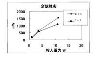
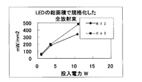
- FIG. 20 and Table 1 show the measurement results of the total radiant flux when the phosphor dome is not covered. The difference is small up to about 3.5 W input power to the light source device. However, at 11 W input power, the total radiant flux of the light source device of Example 2 is 1500 mW or more, which is about 40 times that of the light source device of Comparative Example 2. % Exceeded. Further, the total radiant flux (mW / mm 2 ) normalized by the total area of the LED chip is shown in FIG. In this case, the total area of the LED chip is 0.9 (mm) ⁇ 0.9 (mm) ⁇ 4 (chip), which is 3.24 mm 2 .
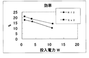
- FIG. 22 and Table 3 show the efficiency of the light source device in a state where the phosphor dome is not covered, as a ratio of the total radiant flux to the total input power.
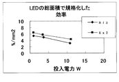
- FIG. 23 and Table 4 show the efficiency of the light source device normalized by the total area of the LED chip.
- the efficiency of the light source device of Example 2 exceeded that of Comparative Example 2 when the input power was 1 W to 11 W, and the difference between the two was more remarkable particularly when the input power was 10 W or more.
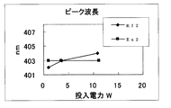
- FIG. 24 and Table 5 show how the emission peak wavelength of the light source device changes with respect to the input power when the phosphor dome is not covered.
- the red shift of the emission wavelength of the LED element that occurs with an increase in input power is generally caused by band gap shrinkage of the active layer due to a temperature rise. Therefore, the large red shift observed in the light source device of Comparative Example 2 suggests that the temperature rise of the LED element accompanying the increase in input power is large.
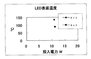
- FIG. 25 shows the measurement result of the surface temperature of the LED chip when the input power is 11 W in a state where the phosphor dome is not covered.
- the temperature was 88 ° C.
- the temperature was 135 ° C., and a temperature difference of about 50 ° C. was observed between the two. It should be noted that in the light source device of Example 2, the surface temperature of the LED chip was below 100 ° C. even though a large power of 11 W was applied.
- FIG. 26 and Table 6 show the measurement results of the total luminous flux when the white light source device is configured using the phosphor dome.
- the total luminous flux of the white light source device of Example 2 exceeds that of Comparative Example 2.
- the former is about 50% higher than the latter. It was higher.
- 27 and Table 7 show the results normalized by the total area of the LED chip.
- the total luminous flux normalized by the total area of the LED chip exceeded 40 Lm / mm 2 when the input power was 11 W.
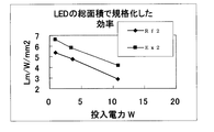
- FIG. 28 and Table 8 show the luminous efficiency when a white light source device is configured using a phosphor dome, expressed as a ratio of total luminous flux to input power (Lm / W).
- Lm / W total luminous flux to input power
- the efficiency of the white light source device of Example 2 exceeds that of Comparative Example 2. Particularly, when the input power is 11W, the former exceeds the latter by about 50%. It was.
- FIG. 29 and Table 9 show the results normalized by the total area of the LED chip. In the white light source device of Example 2, the luminous efficiency normalized with the total area of the LED chip exceeded 4.0 Lm / W / mm 2 when the input power was 11 W.
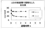
- FIG. 30 and Table 10 show the temporal change of the total luminous flux when the white light source device constituting the phosphor dome is continuously driven with an input power of 11 W. Until the elapse of 3 hours from the start of energization, the total luminous flux of the white light source device of Example 2 exceeded that of Comparative Example 2.
- FIG. 31 and Table 11 show the results normalized by the total area of the LED chip. In the white light source device of Example 2, the total luminous flux normalized by the total area of the LED chip exceeded 40 Lm / mm 2 even after 3 hours had elapsed from the start of energization.
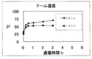
- FIG. 32 and Table 12 show changes over time in the surface temperature of the phosphor dome when the white light source device configured using the phosphor dome is continuously driven at an input power of 11 W.
- FIG. The phosphor dome surface temperature of the white light source device of Example 2 is kept lower than that of Comparative Example 2 until 3 hours have elapsed since the start of energization, and in particular, the former after 30 minutes had elapsed since the start of energization, It was kept constant at about 50 ° C. This suggests that the surface temperature of the phosphor dome can be further lowered when the heat sink bonded to the metal substrate is replaced with one having a higher heat dissipation capability. If the temperature rise of the phosphor dome is suppressed, it is possible to reduce the heat resistance requirement for the members (phosphor, transparent resin, etc.) forming the phosphor dome, and to prevent the wavelength conversion efficiency of the phosphor from decreasing.
- FIG. 33 and Table 13 show changes with time in the substrate surface temperature when the light source device is continuously driven at an input power of 11 W.
- the substrate surface temperature is the temperature of the light source mounting surface (surface of the Au layer to which the LED chip is bonded) of the metal substrate in the light source device of Example 2, while the light source device of Comparative Example 2 is used. Then, it is the surface temperature of the wiring pattern part to which the SMD type package of the insulating Al substrate is joined.
- the substrate surface temperature of the white light source device of Example 2 is kept lower than that of Comparative Example 2 until 3 hours after the start of energization. In particular, the former is about 45 after 15 minutes have elapsed from the start of energization. It was kept constant at ° C. At such a low temperature, heat deterioration of the heat-dissipating aluminum plate is completely prevented.
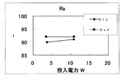
- FIG. 34 shows a color rendering evaluation result when a white light source device is configured using a phosphor dome.
- the white light source device of Comparative Example 2 when the input power was increased from 3.5 W to 11 W, the average color rendering index Ra changed, but in the white light source device of Example 2, a change in color rendering was observed. There wasn't. This suggests that in the white light source device of Example 2, the change in the light emission characteristics of the LED chip with an increase in input power is extremely small.
- Metal substrate 111 211, 411, 511, 611, 711 Al plate 311 Cu plate 112, 212, 412, 512, 612, 712 Ni layer 113, 213, 313, 413, 513, 613, 713 Ni layer 114, 214, 314, 414, 514, 614, 714 Au layer 120, 221, 222, 321, 322, 420, 520, 620, 720 White film 120a, 221a, 222a, 321a 322a, 420a Through holes 131, 231, 331, 431, 531, 631, 731 Cu foil 132, 232, 332, 432, 532, 632, 732 Ni layers 133, 233, 333, 433, 533, 633, 733 Au Layers 10, 11 LED chips 20, 21, Second bonding wires 30 submount 31 ceramic plates 32 and 33 metallized layer M resin mold R D phosphor dome R S phosphor sheet F frame
Abstract
Provided is a metal substrate with which a semiconductor chip to be a light source can be firmly bonded using a metal bonding material and heat generated by the semiconductor chip mounted thereon can be efficiently dissipated via a metal plate. A light source device is also provided.
The metal substrate (100) has the light source mounting surface for mounting the semiconductor chip to be the light source. The metal substrate also has the heat dissipating metal plate (111) composed of a metal other than Au, a white film (120), which is laminated on a part of the heat dissipating metal plate (11) and is composed of an insulating resin, and a light source mounting surface forming layer (114), which is laminated on other part of the heat dissipating metal plate (111). The light source mounting surface forming layer (114) is a metal layer that is directly in contact with the heat dissipating metal plate, and the light source mounting surface is the surface of an Au layer that is the topmost layer of the light source mounting surface forming layer.
Description
本発明は、光源となる半導体チップ、特に発光ダイオードチップ(以下、「LEDチップ」ともいう。)を搭載するための金属基板及びこれを用いた光源装置に関し、より詳しくは、LEDチップを強固に固定できるとともに、LEDチップで発生する熱を効率よく放散させることのできる金属基板に関するものである。
The present invention relates to a metal substrate for mounting a semiconductor chip serving as a light source, particularly a light-emitting diode chip (hereinafter also referred to as “LED chip”), and a light source device using the metal substrate. The present invention relates to a metal substrate that can be fixed and can efficiently dissipate heat generated by an LED chip.
次世代の光源として注目される発光ダイオード(以下、「LED」ともいう。)の用途は、液晶バックライトあるいは自動車用ランプから、照明分野全体へと着実に拡がっている。
LEDチップを用いた光源装置としては、白色銅張積層板から作製したプリント配線基板上にLEDチップを搭載後、透明なシリコーン樹脂あるいはエポキシ樹脂で樹脂封止して製造されるチップ型LEDがある。また、インサート成形によりリードフレームを白色樹脂リフレクターに埋め込んで複合化したパッケージの、白色樹脂リフレクターで囲まれるリードフレーム部にLEDチップを搭載し、リフレクター内部に封止樹脂を充填して製造されるチップ型LEDがある。これらのチップ型LEDは、電子機器のマザー配線基板に半田実装される。 Applications of light-emitting diodes (hereinafter also referred to as “LEDs”) that are attracting attention as next-generation light sources are steadily expanding from the liquid crystal backlights or automobile lamps to the entire lighting field.
As a light source device using an LED chip, there is a chip-type LED manufactured by mounting an LED chip on a printed wiring board manufactured from a white copper clad laminate and then sealing with a transparent silicone resin or epoxy resin. . In addition, a chip manufactured by mounting an LED chip on the lead frame part surrounded by the white resin reflector of the package in which the lead frame is embedded in the white resin reflector by insert molding and compounded, and filling the sealing resin inside the reflector There is a type LED. These chip-type LEDs are solder-mounted on a mother wiring board of an electronic device.
一般照明用途のLED光源装置では、高出力のLEDチップをひとつの配線基板上に複数個搭載する場合が多いことから、LEDチップが発する熱を効率よく放散させて、表面温度の上昇を抑えることが重要となる。LEDチップの表面温度が上昇すると、LEDチップの寿命あるいは発光効率が低下するからである。そのための一手段として、マザー配線基板にLEDチップを直接固定する方式が提案されている。そして、そのマザー配線基板そのものの放熱特性も良好でなくてはならないことから、絶縁金属基板の使用が盛んに検討されている。絶縁金属基板は、放熱フィラーが充填された熱硬化性樹脂層を絶縁層とする配線基板が、金属板上に積層された構造を有するものである。しかし、LEDチップは絶縁樹脂層上に搭載されることになるため、放熱特性が十分ではない。
In LED light source devices for general lighting applications, multiple high-power LED chips are often mounted on a single wiring board, so the heat generated by the LED chips is efficiently dissipated and the rise in surface temperature is suppressed. Is important. This is because when the surface temperature of the LED chip increases, the lifetime or the light emission efficiency of the LED chip decreases. As one means for that purpose, a method of directly fixing an LED chip to a mother wiring board has been proposed. And since the heat dissipation characteristic of the mother wiring substrate itself must be good, the use of an insulating metal substrate has been actively studied. The insulating metal substrate has a structure in which a wiring substrate having a thermosetting resin layer filled with a heat radiation filler as an insulating layer is laminated on a metal plate. However, since the LED chip is mounted on the insulating resin layer, the heat dissipation characteristics are not sufficient.
したがって、より放熱特性に優れたLEDチップ搭載用基板が求められている。この要求に対し、特許文献1及び特許文献2には、LEDチップの搭載部位(キャビティの底面)に金属板を露出させた金属基板が提案されている。
Therefore, there is a demand for a substrate for mounting an LED chip that has more excellent heat dissipation characteristics. In response to this requirement, Patent Document 1 and Patent Document 2 propose a metal substrate in which a metal plate is exposed at an LED chip mounting site (bottom surface of a cavity).
特許文献1のLEDチップ搭載用基板においては、LEDチップを金属板上に直接搭載することが可能である。しかし、この文献に開示されたLED光源装置では、LEDチップと金属板の接合に、熱伝導性が必ずしも良好とはいえない銀ペーストが使用されている。これは、LEDチップ搭載面がAl(アルミニウム)の表面であるため、熱伝導性が高い半田を接合材として用いることができないためである。
In the LED chip mounting substrate of Patent Document 1, the LED chip can be directly mounted on a metal plate. However, in the LED light source device disclosed in this document, a silver paste that is not necessarily good in thermal conductivity is used for joining the LED chip and the metal plate. This is because, since the LED chip mounting surface is an Al (aluminum) surface, solder having high thermal conductivity cannot be used as a bonding material.
一方、特許文献2には、Al板の表面にAu(金)メッキ又はAg(銀)メッキの表面処理を行ない、その上にLEDチップを直接搭載することが記載されている。Auメッキ層の表面には、半田を用いてLEDチップを強固に固定することが可能である。しかし、Al板の表面には蒸着法などの乾式プロセスによりAuメッキが可能ではあるものの、AlとAuの界面では常温ですら激しい合金化反応が発生し、着色物質の生成と、物性の低下が生じる。着色物質の生成は、光源装置にとっては好ましくない。
On the other hand, Patent Document 2 describes that surface treatment of Au (gold) plating or Ag (silver) plating is performed on the surface of an Al plate, and an LED chip is directly mounted thereon. The LED chip can be firmly fixed to the surface of the Au plating layer using solder. However, although the surface of the Al plate can be Au plated by a dry process such as vapor deposition, a severe alloying reaction occurs even at room temperature at the interface between Al and Au, resulting in the formation of colored substances and the deterioration of physical properties. Arise. The generation of the coloring substance is not preferable for the light source device.
そこで、本発明の主たる課題は、光源となる半導体チップを、金属接合材を用いて強固に接合することができ、かつ、搭載された半導体チップで発生する熱を、金属板を通して効率よく放散させることが可能な、金属基板を提供することである。
また、本発明の他の課題は、発生する熱が金属基板を通して効率よく放散されることによって、光源として搭載される半導体チップの表面温度の上昇が抑えられた光源装置を提供することである。 Therefore, the main problem of the present invention is that a semiconductor chip serving as a light source can be firmly bonded using a metal bonding material, and heat generated in the mounted semiconductor chip is efficiently dissipated through the metal plate. It is to provide a metal substrate that is possible.
Another object of the present invention is to provide a light source device in which an increase in surface temperature of a semiconductor chip mounted as a light source is suppressed by efficiently dissipating generated heat through a metal substrate.
本発明は上記課題を解決するためになされたものであり、以下を要旨とするものである。
The present invention has been made in order to solve the above-mentioned problems, and has the following gist.
第1の発明によれば、光源となる半導体チップを搭載するための光源搭載面を有する金属基板であって、Au以外の金属からなる放熱金属板と、該放熱金属板上の一部に積層された絶縁樹脂製の白色フィルムと、該放熱金属板上の他の一部に積層された光源搭載面形成層と、を有し、前記光源搭載面形成層は前記放熱金属板と直接接する金属層であり、前記光源搭載面は前記光源搭載面形成層の最表層をなすAu層の表面である、ことを特徴とする金属基板が提供される。
According to the first invention, there is provided a metal substrate having a light source mounting surface for mounting a semiconductor chip serving as a light source, and is laminated on a part of the heat dissipating metal plate made of a metal other than Au. A white film made of insulating resin, and a light source mounting surface forming layer laminated on another part of the heat radiating metal plate, and the light source mounting surface forming layer is a metal in direct contact with the heat radiating metal plate A metal substrate is provided, wherein the light source mounting surface is a surface of an Au layer that is an outermost layer of the light source mounting surface forming layer.
第1の発明に係る金属基板において、好ましくは、白色フィルムの波長400nm~800nmの範囲における平均反射率は70%以上である。
In the metal substrate according to the first invention, preferably, the average reflectance of the white film in the wavelength range of 400 nm to 800 nm is 70% or more.
第1の発明に係る金属基板において、好ましくは、白色フィルムの260℃で5分間熱処理した後の波長470nmにおける反射率の低下率は10%以下である。
In the metal substrate according to the first aspect of the present invention, preferably, the reduction rate of the reflectance at a wavelength of 470 nm after heat treatment of the white film at 260 ° C. for 5 minutes is 10% or less.
第1の発明に係る金属基板において、白色フィルムはMD(フィルムの流れ方向)及びTD(流れ方向と直交する方向)を有していてもよく、その場合、好ましくは、MDの線膨張係数及びTDの線膨張係数の平均値は35×10-6/℃以下である。
In the metal substrate according to the first invention, the white film may have MD (film flow direction) and TD (direction orthogonal to the flow direction). In that case, preferably, the linear expansion coefficient of MD and The average value of the linear expansion coefficient of TD is 35 × 10 −6 / ° C. or less.
第1の発明に係る金属基板において、好ましくは、白色フィルムは貫通孔を有しており、光源搭載面形成層は該貫通孔の位置に形成されている。
第1の発明に係る金属基板において、好ましくは、前記光源搭載面形成層は最表層をなすAu層の直下にNi層を含む。 In the metal substrate according to the first invention, preferably, the white film has a through hole, and the light source mounting surface forming layer is formed at the position of the through hole.
In the metal substrate according to the first aspect of the present invention, preferably, the light source mounting surface forming layer includes a Ni layer immediately below the outermost Au layer.
第1の発明に係る金属基板において、好ましくは、白色フィルムは複数の貫通孔を有しており、光源搭載面形成層は該複数の貫通孔のそれぞれの位置に形成されている。
In the metal substrate according to the first aspect of the present invention, preferably, the white film has a plurality of through holes, and the light source mounting surface forming layer is formed at each position of the plurality of through holes.
第2の発明によれば、光源となる半導体チップと、該半導体チップを搭載するための光源搭載面を有する金属基板とを備え、該半導体チップが該光源搭載面上に搭載された光源装置であって、該金属基板が、Au以外の金属からなる放熱金属板と、該放熱金属板上の一部に積層された絶縁樹脂製の白色フィルムと、該放熱金属板上の他の一部に積層された光源搭載面形成層と、を有し、前記光源搭載面形成層は前記放熱金属板と直接接する金属層であり、前記光源搭載面は前記光源搭載面形成層の最表層をなすAu層の上面である、ことを特徴とする光源装置が提供される。
According to a second aspect of the present invention, there is provided a light source device including a semiconductor chip serving as a light source and a metal substrate having a light source mounting surface for mounting the semiconductor chip, the semiconductor chip being mounted on the light source mounting surface. The metal substrate is a heat radiating metal plate made of a metal other than Au, a white film made of insulating resin laminated on a part of the heat radiating metal plate, and another part of the heat radiating metal plate. A light source mounting surface forming layer, wherein the light source mounting surface forming layer is a metal layer in direct contact with the heat radiating metal plate, and the light source mounting surface is an outermost layer of the light source mounting surface forming layer. There is provided a light source device characterized in that it is an upper surface of a layer.
第2の発明に係る光源装置において、前記半導体チップは垂直電極型のLEDチップ、又は、導電性基板を有する水平電極型のLEDチップであってもよく、その場合、好ましくは、前記半導体チップは前記光源搭載面上に固定されたサブマウント上に固定される。
In the light source device according to the second invention, the semiconductor chip may be a vertical electrode type LED chip or a horizontal electrode type LED chip having a conductive substrate. In this case, preferably, the semiconductor chip is It is fixed on a submount fixed on the light source mounting surface.
第2の発明に係る光源装置において、前記サブマウントは、好ましくは、セラミック板と、その各主面にそれぞれ形成されたメタライズ層と、を備えている。
In the light source device according to the second invention, the submount preferably includes a ceramic plate and a metallization layer formed on each main surface thereof.
第2の発明に係る光源装置は、前記半導体チップが放出する1次光を吸収して、該1次光の波長とは異なる波長を有する2次光を放出する蛍光体を備えるものであってもよい。その場合の好適例では、蛍光体が、前記半導体チップ及び前記光源搭載面から離れた位置に、空隙を挟んで配置される。
A light source device according to a second aspect of the invention includes a phosphor that absorbs primary light emitted from the semiconductor chip and emits secondary light having a wavelength different from the wavelength of the primary light. Also good. In a preferred example in that case, the phosphor is disposed at a position away from the semiconductor chip and the light source mounting surface with a gap therebetween.
第1の発明に係る金属基板は、光源搭載面がAu層の表面であることから、光源となる半導体チップを、金属接合材(例えばAuSn共晶半田)を用いて該光源搭載面に強固に接合することが可能である。こうして搭載された半導体チップで発生する熱は、放熱金属基板を通して効率よく放散される。従って、この金属基板は、高出力の光源装置に好ましく用いることができる。
In the metal substrate according to the first aspect of the invention, since the light source mounting surface is the surface of the Au layer, the semiconductor chip serving as the light source is firmly attached to the light source mounting surface using a metal bonding material (for example, AuSn eutectic solder). It is possible to join. The heat generated in the semiconductor chip thus mounted is efficiently dissipated through the heat dissipation metal substrate. Therefore, this metal substrate can be preferably used for a high-output light source device.
また、第2の発明に係る光源装置は、発生する熱が金属基板を通して効率よく放散されることによって、半導体チップの表面温度の上昇が抑えられるので、発光効率の低下あるいは、寿命低下が抑制されたものとなる。
Further, in the light source device according to the second invention, since the generated heat is efficiently dissipated through the metal substrate, an increase in the surface temperature of the semiconductor chip is suppressed, so that a decrease in light emission efficiency or a decrease in lifetime is suppressed. It will be.
以下、本発明を具体的実施形態に即して詳しく説明するが、本発明の範囲が以下に説明する実施形態に限定されるものではない。
Hereinafter, the present invention will be described in detail according to specific embodiments, but the scope of the present invention is not limited to the embodiments described below.
<第1の実施形態>
第1の実施形態に係る金属基板の断面図を図1に示す。金属基板100は、放熱金属板として、片側全面にNi層112が積層されたAl板111を有している。Ni層112上の一部には絶縁樹脂製の白色フィルム120が積層されている。白色フィルム120上には、Cu箔131からなる配線パターンが形成されている。Cu箔131上にはNi層132とAu層133がこの順に積層されている。白色フィルム120はその一部に貫通孔120aを有しており、その貫通孔の位置に露出したNi層112上には、Ni層113を介してAu層114が積層されている。Au層114の表面が光源搭載面である。 <First Embodiment>
A cross-sectional view of a metal substrate according to the first embodiment is shown in FIG. Themetal substrate 100 has an Al plate 111 having a Ni layer 112 laminated on the entire surface of one side as a heat radiating metal plate. A white film 120 made of an insulating resin is laminated on a part of the Ni layer 112. On the white film 120, a wiring pattern made of Cu foil 131 is formed. On the Cu foil 131, a Ni layer 132 and an Au layer 133 are laminated in this order. The white film 120 has a through hole 120 a in a part thereof, and an Au layer 114 is laminated on the Ni layer 112 exposed at the position of the through hole via the Ni layer 113. The surface of the Au layer 114 is a light source mounting surface.
第1の実施形態に係る金属基板の断面図を図1に示す。金属基板100は、放熱金属板として、片側全面にNi層112が積層されたAl板111を有している。Ni層112上の一部には絶縁樹脂製の白色フィルム120が積層されている。白色フィルム120上には、Cu箔131からなる配線パターンが形成されている。Cu箔131上にはNi層132とAu層133がこの順に積層されている。白色フィルム120はその一部に貫通孔120aを有しており、その貫通孔の位置に露出したNi層112上には、Ni層113を介してAu層114が積層されている。Au層114の表面が光源搭載面である。 <First Embodiment>
A cross-sectional view of a metal substrate according to the first embodiment is shown in FIG. The
金属基板100の製造工程を、図2(a)~(d)を用いて説明する。
まず、図2(a)に示すように、白色フィルム120の片面にCu箔131を積層して銅張積層板を形成する。 A manufacturing process of themetal substrate 100 will be described with reference to FIGS.
First, as shown to Fig.2 (a),Cu foil 131 is laminated | stacked on the single side | surface of the white film 120, and a copper clad laminated board is formed.
まず、図2(a)に示すように、白色フィルム120の片面にCu箔131を積層して銅張積層板を形成する。 A manufacturing process of the
First, as shown to Fig.2 (a),
次に、図2(b)に示すように、Cu箔131をエッチングして配線パターンを形成し、さらにビク型などの打ち抜き型を用いて白色フィルム120の一部を打ち抜き、貫通孔120aを形成する。
Next, as shown in FIG. 2B, the Cu foil 131 is etched to form a wiring pattern, and a part of the white film 120 is punched using a punching die such as a big die to form a through hole 120a. To do.
次に、図2(c)に示すように、白色フィルム120の、配線パターン(Cu箔131)が形成された面とは反対面に、放熱金属板として、予め片側全面にNi層112が積層されたAl板111を真空プレスにて積層する。Al板111の厚さは、例えば、0.1mm~5mmとすることができる。実際的には、製造しようとする金属基板100のサイズを勘案のうえ、必要な強度が得られる厚さのAl板111を選択する。Ni層112は無電解メッキ処理により形成されている。Al板111の無電解Niメッキでは、前処理として、Al板111表面をアルカリ等でエッチングし、更に硝酸等で酸処理を行った後、アルカリ性亜鉛置換液により亜鉛置換する。Ni層112の厚さは、0.1μm~10μmとすることができる。
Next, as shown in FIG. 2C, a Ni layer 112 is previously laminated on the entire surface of one side as a heat dissipation metal plate on the surface of the white film 120 opposite to the surface on which the wiring pattern (Cu foil 131) is formed. The laminated Al plate 111 is laminated by a vacuum press. The thickness of the Al plate 111 can be set to 0.1 mm to 5 mm, for example. In practice, the Al plate 111 having a thickness that provides the required strength is selected in consideration of the size of the metal substrate 100 to be manufactured. The Ni layer 112 is formed by an electroless plating process. In the electroless Ni plating of the Al plate 111, as a pretreatment, the surface of the Al plate 111 is etched with an alkali or the like, and further subjected to an acid treatment with nitric acid or the like, followed by zinc substitution with an alkaline zinc substitution solution. The thickness of the Ni layer 112 can be 0.1 μm to 10 μm.
なお、Ni層112は真空蒸着法あるいはスパッタリング法などの乾式法で形成することも可能であり、その場合には、亜鉛置換処理は不要となる。しかし、湿式メッキ処理の方が多数枚のAl板111を一括処理できることから、乾式法よりも大量生産に適している。
Note that the Ni layer 112 can also be formed by a dry method such as a vacuum evaporation method or a sputtering method, in which case the zinc replacement treatment is not necessary. However, the wet plating process is more suitable for mass production than the dry process because a large number of Al plates 111 can be processed at once.
最後に、図2(d)に示すように、白色フィルムの貫通孔120aを通して露出するNi層112の表面に、無電解メッキ技法を用いてNi層113及びAu層114をこの順に形成する。このとき、同時に、配線パターンを構成するCu箔131の表面にもNi層132とAu層133が形成される。この工程で形成するNi層132の厚さは、好ましくは2μm~8μmである。Au層の厚さについては、0.01μm~10μmとすることができるが、Cu箔131上に形成されるAu層133のワイヤボンディング性を良好なものとするために、好ましくは0.1μm以上、より好ましくは0.3μm以上、更に好ましくは0.5μm以上とする。ただし、これより薄く形成した場合であっても、表面のプラズマ処理によりAu層133のワイヤボンディング性を改善することが可能である。厚いAu層を形成することはコスト上昇を招くので、この工程で形成するAu層の厚さは好ましくは2μm以下、より好ましくは1μm以下である。
Finally, as shown in FIG. 2D, a Ni layer 113 and an Au layer 114 are formed in this order on the surface of the Ni layer 112 exposed through the through-hole 120a of the white film by using an electroless plating technique. At the same time, the Ni layer 132 and the Au layer 133 are also formed on the surface of the Cu foil 131 constituting the wiring pattern. The thickness of the Ni layer 132 formed in this step is preferably 2 μm to 8 μm. The thickness of the Au layer can be 0.01 μm to 10 μm, but is preferably 0.1 μm or more in order to improve the wire bonding property of the Au layer 133 formed on the Cu foil 131. More preferably, it is 0.3 μm or more, and further preferably 0.5 μm or more. However, even if it is formed thinner than this, the wire bonding property of the Au layer 133 can be improved by the plasma treatment of the surface. Since the formation of a thick Au layer causes an increase in cost, the thickness of the Au layer formed in this step is preferably 2 μm or less, more preferably 1 μm or less.
殆ど全ての樹脂はAuに対して強く接着しないが、金属基板100では、白色フィルム120がAu層114上に積層された部分を有さず、その下面全体が、Ni層112に接していることから、白色フィルム120の剥離が生じ難い。また、配線パターン上を除けば、LEDチップを搭載する領域のみにAu層を形成しているので、高価なAuの使用量が少なく抑えられている。
Almost all of the resin does not adhere strongly to Au, but the metal substrate 100 does not have a portion where the white film 120 is laminated on the Au layer 114, and the entire lower surface thereof is in contact with the Ni layer 112. Therefore, the white film 120 hardly peels off. Moreover, since the Au layer is formed only in the area where the LED chip is mounted except on the wiring pattern, the amount of expensive Au used is reduced.
また、Auの表面は波長550nm未満における反射率が著しく低いため、出力光に短波長の可視光成分を含む光源装置、例えば、青色光源装置あるいは白色光源装置におけるAuの使用は、発光効率を低下させる場合がある。この問題を解決するために、金属基板100ではAuの使用を光源搭載面に限定しており、さらに、光源搭載面以外の金属板表面を白色フィルム120で覆うことにより、可視光に対する反射率の向上を図っている。
In addition, since the reflectance of the surface of Au is significantly low at a wavelength of less than 550 nm, the use of Au in a light source device that includes a short-wavelength visible light component in the output light, for example, a blue light source device or a white light source device, reduces luminous efficiency. There is a case to let you. In order to solve this problem, in the metal substrate 100, the use of Au is limited to the light source mounting surface, and further, the surface of the metal plate other than the light source mounting surface is covered with the white film 120, so We are trying to improve.
また、金属基板100では、Au層114の形成前に、Al板111に対しNiメッキ処理を2回行っているので、Al板111とAu層114との間が2つのNi層112、113で隔てられている。そのため、AlとAuとが接したとき生じる有害な合金化反応が確実に防止されている。
Further, in the metal substrate 100, since the Ni plating process is performed twice on the Al plate 111 before the Au layer 114 is formed, there are two Ni layers 112 and 113 between the Al plate 111 and the Au layer 114. It is separated. Therefore, harmful alloying reaction that occurs when Al and Au come into contact with each other is reliably prevented.
図3に、金属基板100を用いて構成した光源装置の断面図を示す。この光源装置は、光源搭載面たるAu層114の表面に、Au-Sn半田などのろう材(図示せず)を用いてLEDチップ10を固定し、更にボンディングワイヤ20により配線パターン(Cu箔131)と接続させることにより、得られる。光源搭載面が半田の濡れ性の良好なAuからなるために、LEDチップ10と光源搭載面の結合は強固なものとなる。
FIG. 3 shows a cross-sectional view of a light source device configured using the metal substrate 100. In this light source device, the LED chip 10 is fixed to the surface of the Au layer 114 serving as a light source mounting surface by using a brazing material (not shown) such as Au—Sn solder, and a wiring pattern (Cu foil 131) is further formed by bonding wires 20. ) To obtain. Since the light source mounting surface is made of Au having good solder wettability, the LED chip 10 and the light source mounting surface are firmly coupled.
金属基板100にLEDチップを実装するにあたっては、図4に示すように、サブマウントを用いることも可能である。サブマウントの使用は、特に、半導体または金属からなる導電性基板上に半導体発光素子構造が形成された、垂直電極型のLEDチップを実装する場合に有効である。この場合には、図5に示すような、極めてシンプルな構造のサブマントを好ましく用いることができる。
When mounting the LED chip on the metal substrate 100, it is also possible to use a submount as shown in FIG. The use of the submount is particularly effective when a vertical electrode type LED chip having a semiconductor light emitting element structure formed on a conductive substrate made of a semiconductor or metal is mounted. In this case, a submant having a very simple structure as shown in FIG. 5 can be preferably used.
図5に示すサブマウント30は、AlN、アルミナなどからなるセラミック板31の各主面31a、31bに、メタライズ層32、33をそれぞれ有してなるものである。セラミック板31の厚さは好ましくは0.1mm~0.5mm、メタライズ層32、33の厚さは、好ましくは0.1μm~10μmである。いずれのメタライズ層32、33も、最表層は半田の濡れ性が良好な金属で形成する。また、メタライズ層32、33の少なくとも一方は、半田の濡れ性とワイヤボンディング性の両方に優れる金属、例えばAuで、最表層を形成することが望ましい。最表層をAu層とする好ましいメタライズ層は、例えば、セラミック板と接する側から順に、Ti/Pt/Au、Ti/Ni/Au、Cr/Au、Ti/Auなどの積層構造を有する多層膜である。ワイヤボンディング性を良好にするためには、Au層の厚さは好ましくは0.1μm以上、より好ましくは0.3μm以上、特に好ましくは0.5μm以上とする。厚いAu層を形成することはコスト上昇を招くので、Au層の膜厚は好ましくは2μm以下、より好ましくは1μm以下である。
The submount 30 shown in FIG. 5 has metallized layers 32 and 33 on main surfaces 31a and 31b of a ceramic plate 31 made of AlN, alumina, or the like. The thickness of the ceramic plate 31 is preferably 0.1 mm to 0.5 mm, and the thickness of the metallized layers 32 and 33 is preferably 0.1 μm to 10 μm. In any of the metallized layers 32 and 33, the outermost layer is formed of a metal having good solder wettability. Further, it is desirable that at least one of the metallized layers 32 and 33 is made of a metal excellent in both solder wettability and wire bonding property, for example, Au, and the outermost layer is formed. A preferable metallized layer whose outermost layer is an Au layer is, for example, a multilayer film having a laminated structure of Ti / Pt / Au, Ti / Ni / Au, Cr / Au, Ti / Au, etc. in order from the side in contact with the ceramic plate. is there. In order to improve the wire bonding property, the thickness of the Au layer is preferably 0.1 μm or more, more preferably 0.3 μm or more, and particularly preferably 0.5 μm or more. Since forming a thick Au layer causes an increase in cost, the thickness of the Au layer is preferably 2 μm or less, more preferably 1 μm or less.
上述のサブマウント30を用いて、導電性基板を備えた垂直電極型のLEDチップ11を金属基板100に搭載してなる光源装置の断面図を、図6に示す。この光源装置において、光源搭載面を与えるAu層114とサブマウント30(メタライズ層32)との間、及び、サブマウント30(メタライズ層33)とLEDチップ11との間は、それぞれ半田(図示せず)により接続されている。LEDチップ11の上面側の電極は、ボンディングワイヤ21により一方の配線パターンに接続されている。他方、LEDチップ11の下面側の電極は、メタライズ層33及びボンディングワイヤ22を経由して他方の配線パターンに接続されている。Al基板111とLEDチップ11との間は、サブマウント30に含まれるセラミック板31によって絶縁されている。
FIG. 6 shows a cross-sectional view of a light source device in which the vertical electrode type LED chip 11 having a conductive substrate is mounted on the metal substrate 100 using the submount 30 described above. In this light source device, solder (not shown) is provided between the Au layer 114 providing the light source mounting surface and the submount 30 (metallized layer 32), and between the submount 30 (metalized layer 33) and the LED chip 11. Connected). The electrode on the upper surface side of the LED chip 11 is connected to one wiring pattern by a bonding wire 21. On the other hand, the electrode on the lower surface side of the LED chip 11 is connected to the other wiring pattern via the metallized layer 33 and the bonding wire 22. The Al substrate 111 and the LED chip 11 are insulated by a ceramic plate 31 included in the submount 30.
垂直電極型のLEDチップ11は、例えば、米国特許公開公報2006/0154389号明細書に開示された、チップ中に支持基板として金属基板を有するLEDチップ、日本国特開2006-179511号公報に開示された、GaN基板を用いて製造されるLEDチップ、Japanese Journal of Applied Physics第49巻022101頁(2010年)に開示された、チップ中に支持基板として半導体基板(Si基板)を有するLEDチップ、などである。
導電性基板を用いた水平電極型のLEDチップであって、正負の電極が設けられた側のチップ面から光を取り出すタイプのLEDチップを、金属基板100に搭載する場合にも、上述のサブマウント30を好ましく用いることができる。このようなLEDチップは、例えば、国際公開第2008/004437号に記載されている(GaN基板を用いたLEDチップ)。サブマウント30を用いると、セラミック板31によって、LEDチップの導電性基板と、金属基板の放熱金属板とが絶縁されるため、漏電が防止できる他、ひとつの金属基板上に複数のLEDチップを搭載する場合には、チップ間配線の自由度が高くなる。 The vertical electrodetype LED chip 11 is disclosed in, for example, US Patent Publication No. 2006/0154389, an LED chip having a metal substrate as a support substrate in the chip, and disclosed in Japanese Patent Application Laid-Open No. 2006-179511. An LED chip manufactured using a GaN substrate, an LED chip disclosed in Japanese Journal of Applied Physics 49: 022211 (2010), having a semiconductor substrate (Si substrate) as a supporting substrate in the chip, Etc.
Even when a horizontal electrode type LED chip using a conductive substrate and taking out light from the chip surface on the side where the positive and negative electrodes are provided is mounted on themetal substrate 100, the above-mentioned sub The mount 30 can be preferably used. Such an LED chip is described in, for example, International Publication No. 2008/004437 (LED chip using a GaN substrate). When the submount 30 is used, the ceramic substrate 31 insulates the conductive substrate of the LED chip from the heat-dissipating metal plate of the metal substrate, so that leakage can be prevented and a plurality of LED chips can be mounted on one metal substrate. In the case of mounting, the degree of freedom of interchip wiring is increased.
導電性基板を用いた水平電極型のLEDチップであって、正負の電極が設けられた側のチップ面から光を取り出すタイプのLEDチップを、金属基板100に搭載する場合にも、上述のサブマウント30を好ましく用いることができる。このようなLEDチップは、例えば、国際公開第2008/004437号に記載されている(GaN基板を用いたLEDチップ)。サブマウント30を用いると、セラミック板31によって、LEDチップの導電性基板と、金属基板の放熱金属板とが絶縁されるため、漏電が防止できる他、ひとつの金属基板上に複数のLEDチップを搭載する場合には、チップ間配線の自由度が高くなる。 The vertical electrode
Even when a horizontal electrode type LED chip using a conductive substrate and taking out light from the chip surface on the side where the positive and negative electrodes are provided is mounted on the
<第2の実施形態>
第2の実施形態に係る金属基板の断面図を図7に示す。金属基板200は、放熱金属板として、片側全面にNi層212が積層されたAl板211を有している。Ni層212上の一部には絶縁樹脂製の第一の白色フィルム221が積層されている。第一の白色フィルム221上には、Cu箔231からなる配線パターンが形成されるとともに、その配線パターンの一部を露出させるように、絶縁樹脂製の第二の白色フィルム222が積層されている。Cu箔231の一部に露出した表面には、Ni層232とAu層233がこの順に積層されている。第一の白色フィルム221及び第二の白色フィルム222は、その一部に貫通孔221a、222aをそれぞれ有しており、これらの貫通孔の位置に露出したNi層212上には、Ni層213を介してAu層214が積層されている。Au層214の表面が光源搭載面である。 <Second Embodiment>
FIG. 7 shows a cross-sectional view of the metal substrate according to the second embodiment. Themetal substrate 200 has an Al plate 211 having a Ni layer 212 laminated on the entire surface of one side as a heat radiating metal plate. A part of the Ni layer 212 is laminated with a first white film 221 made of an insulating resin. On the first white film 221, a wiring pattern made of Cu foil 231 is formed, and a second white film 222 made of an insulating resin is laminated so as to expose a part of the wiring pattern. . A Ni layer 232 and an Au layer 233 are laminated in this order on the surface exposed to a part of the Cu foil 231. The first white film 221 and the second white film 222 respectively have through holes 221a and 222a in a part thereof, and the Ni layer 213 is formed on the Ni layer 212 exposed at the positions of these through holes. The Au layer 214 is laminated via The surface of the Au layer 214 is a light source mounting surface.
第2の実施形態に係る金属基板の断面図を図7に示す。金属基板200は、放熱金属板として、片側全面にNi層212が積層されたAl板211を有している。Ni層212上の一部には絶縁樹脂製の第一の白色フィルム221が積層されている。第一の白色フィルム221上には、Cu箔231からなる配線パターンが形成されるとともに、その配線パターンの一部を露出させるように、絶縁樹脂製の第二の白色フィルム222が積層されている。Cu箔231の一部に露出した表面には、Ni層232とAu層233がこの順に積層されている。第一の白色フィルム221及び第二の白色フィルム222は、その一部に貫通孔221a、222aをそれぞれ有しており、これらの貫通孔の位置に露出したNi層212上には、Ni層213を介してAu層214が積層されている。Au層214の表面が光源搭載面である。 <Second Embodiment>
FIG. 7 shows a cross-sectional view of the metal substrate according to the second embodiment. The
金属基板200の製造工程を、図8(a)~(d)を用いて説明する。
まず、図8(a)に示すように、第一の白色フィルム221の片面にCu箔231を積層して銅張積層板を形成する。 A manufacturing process of themetal substrate 200 will be described with reference to FIGS.
First, as shown to Fig.8 (a),Cu foil 231 is laminated | stacked on the single side | surface of the 1st white film 221, and a copper clad laminated board is formed.
まず、図8(a)に示すように、第一の白色フィルム221の片面にCu箔231を積層して銅張積層板を形成する。 A manufacturing process of the
First, as shown to Fig.8 (a),
次に、図8(b)に示すように、Cu箔231をエッチングして配線パターンを形成し、さらにビク型を用いて第一の白色フィルム221の一部を打ち抜き、第一の貫通孔221aを形成する。
また、別途工程で、第一の白色フィルム221と同じ絶縁樹脂材料からなる第二の白色フィルム222を準備する。この第二の白色フィルム222には、ビク型を用いた打ち抜き加工により、第二の貫通孔222aを形成しておく。第二の白色フィルム222は、第一の白色フィルム221上に形成された配線パターン(Cu箔231)を保護するための保護層となる。図示するように、第二の白色フィルム222の貫通孔222a(50)は、その内側に第一の白色フィルム221の貫通孔221aが収まるように、かつ、Cu箔231からなる配線パターンの一部(ワイヤボンディング端子を形成する部分)が露出するように、その形状及びサイズが設定される。 Next, as shown in FIG. 8 (b), theCu foil 231 is etched to form a wiring pattern, and a part of the first white film 221 is punched out using a big die, so that the first through hole 221a is formed. Form.
In a separate process, a secondwhite film 222 made of the same insulating resin material as the first white film 221 is prepared. In the second white film 222, a second through hole 222a is formed by punching using a big die. The second white film 222 serves as a protective layer for protecting the wiring pattern (Cu foil 231) formed on the first white film 221. As shown in the drawing, the through hole 222a (50) of the second white film 222 is part of the wiring pattern made of the Cu foil 231 so that the through hole 221a of the first white film 221 is accommodated inside the through hole 222a (50). The shape and size are set so that (the part forming the wire bonding terminal) is exposed.
また、別途工程で、第一の白色フィルム221と同じ絶縁樹脂材料からなる第二の白色フィルム222を準備する。この第二の白色フィルム222には、ビク型を用いた打ち抜き加工により、第二の貫通孔222aを形成しておく。第二の白色フィルム222は、第一の白色フィルム221上に形成された配線パターン(Cu箔231)を保護するための保護層となる。図示するように、第二の白色フィルム222の貫通孔222a(50)は、その内側に第一の白色フィルム221の貫通孔221aが収まるように、かつ、Cu箔231からなる配線パターンの一部(ワイヤボンディング端子を形成する部分)が露出するように、その形状及びサイズが設定される。 Next, as shown in FIG. 8 (b), the
In a separate process, a second
次に、図8(c)に示すように、第一の白色フィルム221の、配線パターン(Cu箔231)が形成された面とは反対面に、予め片側全面にNi層212が積層されたAl板211を真空プレスにて積層する。この真空プレス工程では、第一の白色フィルム221上への第2の白色フィルム222の積層も同時に行う。
Next, as shown in FIG.8 (c), Ni layer 212 was previously laminated | stacked on the one side whole surface in the opposite side to the surface in which the wiring pattern (Cu foil 231) was formed of the 1st white film 221. The Al plate 211 is laminated by a vacuum press. In this vacuum pressing step, the second white film 222 is laminated on the first white film 221 at the same time.
最後に、図8(d)に示すように、第一の白色フィルム221の貫通孔221a及び第2の白色フィルム222の貫通孔222aを通して露出するNi層212の表面に、無電解メッキ技法を用いてNi層213及びAu層214をこの順に形成する。このとき、同時に、配線パターン(Cu箔231)の一部露出した表面にも、Ni層232とAu層233が形成される。
Finally, as shown in FIG. 8D, an electroless plating technique is used on the surface of the Ni layer 212 exposed through the through hole 221a of the first white film 221 and the through hole 222a of the second white film 222. Then, the Ni layer 213 and the Au layer 214 are formed in this order. At the same time, the Ni layer 232 and the Au layer 233 are also formed on the partially exposed surface of the wiring pattern (Cu foil 231).
金属基板200における、Al板、Ni層及びAu層の好ましい厚さは、第1の実施形態にかかる金属基板100における対応する構造の好ましい厚さを参照されたい。
For the preferable thicknesses of the Al plate, Ni layer, and Au layer in the metal substrate 200, refer to the preferable thicknesses of the corresponding structures in the metal substrate 100 according to the first embodiment.
図9に、金属基板200を用いて構成した光源装置の断面図を示す。この光源装置は、光源搭載面たるAu層214の表面に、Au-Sn半田などのろう材(図示せず)を用いてLEDチップ10を固定し、更にボンディングワイヤ20により配線パターンと接続させることにより、得られる。光源搭載面が半田の濡れ性の良好なAuからなるために、LEDチップと光源搭載面の結合は強固なものとなる。LEDチップが導電性基板を含み、その導電性基板が光源搭載面側を向くように、このLEDチップを固定する場合には、前述のサブマウント30を好ましく用いることができる。
FIG. 9 shows a cross-sectional view of a light source device configured using the metal substrate 200. In this light source device, the LED chip 10 is fixed to the surface of the Au layer 214 as a light source mounting surface by using a brazing material (not shown) such as Au—Sn solder, and further connected to the wiring pattern by the bonding wires 20. Is obtained. Since the light source mounting surface is made of Au with good solder wettability, the LED chip and the light source mounting surface are strongly bonded. When the LED chip is fixed so that the LED chip includes a conductive substrate and the conductive substrate faces the light source mounting surface, the above-described submount 30 can be preferably used.
<第3の実施形態>
第3の実施形態に係る金属基板の断面図を図10に示す。金属基板300は、放熱金属板としてCu板311を有している。Cu板311上の一部には絶縁樹脂製の第一の白色フィルム321が積層されている。第一の白色フィルム321上には、Cu箔331からなる配線パターンが形成されるとともに、その配線パターン(Cu箔331)の一部を露出させるように、絶縁樹脂製の第二の白色フィルム322が積層されている。配線パターン(Cu箔331)の一部露出した表面には、Ni層332とAu層333がこの順に積層されている。第一の白色フィルム321及び第二の白色フィルム322は、その一部に貫通孔321a、322aをそれぞれ有しており、これらの貫通孔の位置に露出したCu板311の表面に、Ni層313を介してAu層314が積層されている。Au層314の表面が光源搭載面である。 <Third Embodiment>
A cross-sectional view of a metal substrate according to the third embodiment is shown in FIG. Themetal substrate 300 has a Cu plate 311 as a heat radiating metal plate. A first white film 321 made of an insulating resin is laminated on a part of the Cu plate 311. A wiring pattern made of Cu foil 331 is formed on the first white film 321 and a second white film 322 made of an insulating resin is exposed so that a part of the wiring pattern (Cu foil 331) is exposed. Are stacked. On the partially exposed surface of the wiring pattern (Cu foil 331), a Ni layer 332 and an Au layer 333 are laminated in this order. The first white film 321 and the second white film 322 each have through holes 321a and 322a in a part thereof, and a Ni layer 313 is formed on the surface of the Cu plate 311 exposed at the positions of these through holes. An Au layer 314 is laminated via The surface of the Au layer 314 is a light source mounting surface.
第3の実施形態に係る金属基板の断面図を図10に示す。金属基板300は、放熱金属板としてCu板311を有している。Cu板311上の一部には絶縁樹脂製の第一の白色フィルム321が積層されている。第一の白色フィルム321上には、Cu箔331からなる配線パターンが形成されるとともに、その配線パターン(Cu箔331)の一部を露出させるように、絶縁樹脂製の第二の白色フィルム322が積層されている。配線パターン(Cu箔331)の一部露出した表面には、Ni層332とAu層333がこの順に積層されている。第一の白色フィルム321及び第二の白色フィルム322は、その一部に貫通孔321a、322aをそれぞれ有しており、これらの貫通孔の位置に露出したCu板311の表面に、Ni層313を介してAu層314が積層されている。Au層314の表面が光源搭載面である。 <Third Embodiment>
A cross-sectional view of a metal substrate according to the third embodiment is shown in FIG. The
金属基板300の製造工程を、図11(a)~(d)を用いて説明する。
まず、図11(a)に示すように、第一の白色フィルム321の片面にCu箔331を積層して銅張積層板を形成する。 A manufacturing process of themetal substrate 300 will be described with reference to FIGS.
First, as shown to Fig.11 (a),Cu foil 331 is laminated | stacked on the single side | surface of the 1st white film 321, and a copper clad laminated board is formed.
まず、図11(a)に示すように、第一の白色フィルム321の片面にCu箔331を積層して銅張積層板を形成する。 A manufacturing process of the
First, as shown to Fig.11 (a),
次に、図11(b)に示すように、Cu箔331をエッチングして配線パターンを形成し、さらにビク型を用いて第一の白色フィルムの一部を打ち抜き、第一の貫通孔321aを形成する。
また、別途工程で、第一の白色フィルム321と同じ絶縁樹脂材料からなる第二の白色フィルム322を準備する。この第二の白色フィルム322には、ビク型を用いた打ち抜き加工により、第二の貫通孔322aを形成しておく。第二の白色フィルム322は、第一の白色フィルム321上に形成された配線パターン(Cu箔331)を保護するための保護層となる。図示するように、第二の白色フィルム322の貫通孔322aは、その内側に第一の白色フィルムの貫通孔321aが収まるように、かつ、配線パターン(Cu箔331)の一部(ワイヤボンディング端子を形成する部分)が露出するように、その形状及びサイズが設定される。 Next, as shown in FIG. 11 (b), theCu foil 331 is etched to form a wiring pattern, and a part of the first white film is punched out using a big die, and the first through hole 321a is formed. Form.
In a separate process, a secondwhite film 322 made of the same insulating resin material as the first white film 321 is prepared. In the second white film 322, a second through hole 322a is formed by punching using a big die. The second white film 322 serves as a protective layer for protecting the wiring pattern (Cu foil 331) formed on the first white film 321. As shown in the figure, the through hole 322a of the second white film 322 is formed so that the through hole 321a of the first white film is accommodated inside thereof, and a part of the wiring pattern (Cu foil 331) (wire bonding terminal) The shape and size are set so that the portion that forms) is exposed.
また、別途工程で、第一の白色フィルム321と同じ絶縁樹脂材料からなる第二の白色フィルム322を準備する。この第二の白色フィルム322には、ビク型を用いた打ち抜き加工により、第二の貫通孔322aを形成しておく。第二の白色フィルム322は、第一の白色フィルム321上に形成された配線パターン(Cu箔331)を保護するための保護層となる。図示するように、第二の白色フィルム322の貫通孔322aは、その内側に第一の白色フィルムの貫通孔321aが収まるように、かつ、配線パターン(Cu箔331)の一部(ワイヤボンディング端子を形成する部分)が露出するように、その形状及びサイズが設定される。 Next, as shown in FIG. 11 (b), the
In a separate process, a second
次に、図11(c)に示すように、第一の白色フィルム321の、配線パターン(Cu箔331)が形成された面とは反対面に、Cu板311を真空プレスにて積層する。この真空プレス工程では、第一の白色フィルム321上への第2の白色フィルム322の積層も同時に行う。
Next, as shown in FIG. 11C, a Cu plate 311 is laminated on the surface of the first white film 321 opposite to the surface on which the wiring pattern (Cu foil 331) is formed by a vacuum press. In this vacuum pressing step, the second white film 322 is also laminated on the first white film 321 at the same time.
最後に、図11(d)に示すように、第一の白色フィルムの貫通孔321a及び第2の白色フィルムの貫通孔322aを通して露出するCu板311の表面に、無電解メッキ技法を用いてNi層313及びAu層314をこの順に形成する。このとき、同時に、配線パターン(Cu箔331)の一部露出した表面にも、Ni層332とAu層333が形成される。
Finally, as shown in FIG. 11 (d), the surface of the Cu plate 311 exposed through the through hole 321a of the first white film and the through hole 322a of the second white film is subjected to Ni using an electroless plating technique. A layer 313 and an Au layer 314 are formed in this order. At the same time, the Ni layer 332 and the Au layer 333 are also formed on the partially exposed surface of the wiring pattern (Cu foil 331).
金属基板300において、Ni層313は、Cu板311からAu層314にCuが拡散するのを防ぐバリア層として働く。Cuの拡散は、Au層表面の半田濡れ性を低下させる。
In the metal substrate 300, the Ni layer 313 functions as a barrier layer that prevents Cu from diffusing from the Cu plate 311 to the Au layer 314. The diffusion of Cu reduces the solder wettability of the Au layer surface.
金属基板300における、Cu板、Ni層及びAu層の好ましい厚さは、第1の実施形態に係る金属基板100において対応する構造の好ましい厚さを参照されたい。
For the preferable thicknesses of the Cu plate, the Ni layer, and the Au layer in the metal substrate 300, refer to the preferable thicknesses of the corresponding structures in the metal substrate 100 according to the first embodiment.
金属基板300においても、第一の白色フィルム321がAu層314上に積層された部分を有さず、その下面全体がCu板311に接しているので、第一の白色フィルム321の剥離が生じ難い。変形例では、Cu板311の光源搭載面が形成される側の面全体に、Ni層を積層したうえで、第一の白色フィルム321をそのNi層上に積層することもできる。
Also in the metal substrate 300, the first white film 321 does not have a portion laminated on the Au layer 314, and the entire lower surface thereof is in contact with the Cu plate 311, so that the first white film 321 is peeled off. hard. In the modification, the first white film 321 can be laminated on the Ni layer after the Ni layer is laminated on the entire surface of the Cu plate 311 on which the light source mounting surface is formed.
図12に、第3の実施形態に係る金属基板300を用いて構成した光源装置の断面図を示す。この光源装置は、光源搭載面たるAu層314の表面に、Au-Sn半田などのろう材(図示せず)を用いてLEDチップ10を固定し、更にボンディングワイヤ20により配線パターンと接続させることにより、得られる。光源搭載面が半田の濡れ性の良好なAuからなるために、LEDチップと光源搭載面の結合は強固なものとなる。LEDチップが導電性基板を含み、その導電性基板が光源搭載面側を向くようこのLEDチップを固定する場合には、前述のサブマウント30を用いてもよい。
FIG. 12 is a cross-sectional view of a light source device configured using a metal substrate 300 according to the third embodiment. In this light source device, the LED chip 10 is fixed to the surface of the Au layer 314 as a light source mounting surface using a brazing material (not shown) such as Au—Sn solder, and further connected to the wiring pattern by the bonding wires 20. Is obtained. Since the light source mounting surface is made of Au with good solder wettability, the LED chip and the light source mounting surface are strongly bonded. When the LED chip includes a conductive substrate, and the LED chip is fixed so that the conductive substrate faces the light source mounting surface, the above-described submount 30 may be used.
上記の各実施形態において、白色フィルムとパターニングされたCu箔とからなる配線基板は、必要に応じて多層構成(多層配線基板)とすることができる。また、白色フィルムに貫通孔を形成する方法は、上記ビク型を用いる方法に制限されるものではなく、例えば、レーザー加工あるいはルーター加工を用いたものであってもよい。
In each of the above embodiments, the wiring board made of the white film and the patterned Cu foil can have a multilayer structure (multilayer wiring board) as necessary. Moreover, the method of forming a through-hole in a white film is not limited to the method using the above-mentioned big type, and for example, a method using laser processing or router processing may be used.
上記の各実施形態に係る金属基板の製造工程の説明に用いた図面(図2、8及び11)には、1個の金属基板のみが描かれているが、便宜のために過ぎない。大量生産のためには、大面積の放熱金属板を用いて多数の金属基板を一括形成した後、切り分ける方法が適している。
In the drawings (FIGS. 2, 8 and 11) used to describe the manufacturing process of the metal substrate according to each of the above embodiments, only one metal substrate is drawn, but this is for convenience only. For mass production, a method in which a large number of metal substrates are collectively formed using a large-area heat-dissipating metal plate and then cut is suitable.
上記の各実施形態に係る金属基板に搭載することのできるLEDチップに限定はなく、AlGaAs系半導体を用いた赤色LEDチップ、AlGaInP系半導体を用いた黄色LEDチップ、GaP系半導体を用いた緑色LEDチップ、ZnSe系半導体を用いた緑~青色LEDチップ、AlGaInN系半導体を用いた緑色~紫外LEDチップ、ZnO系半導体を用いた青色~紫外LEDチップなど、各種のLEDチップを搭載することができる。また、光源搭載面のサイズは、搭載しようとするLEDチップのサイズ及び数に応じて、適宜設定することができる。
The LED chip that can be mounted on the metal substrate according to each of the above embodiments is not limited, and a red LED chip using an AlGaAs semiconductor, a yellow LED chip using an AlGaInP semiconductor, and a green LED using a GaP semiconductor. Various LED chips such as a chip, a green to blue LED chip using a ZnSe semiconductor, a green to ultraviolet LED chip using an AlGaInN semiconductor, and a blue to ultraviolet LED chip using a ZnO semiconductor can be mounted. Further, the size of the light source mounting surface can be appropriately set according to the size and number of LED chips to be mounted.
上記の各実施形態に係る金属基板を用いて光源装置を製造するにあたり、光源搭載面とLEDチップとの接合に用いる好ましい接合材は半田(ろう材)である。半田による接合が強固に行われるよう、LEDチップの表面も必要に応じてメタライズすることができる。
In manufacturing the light source device using the metal substrate according to each of the above embodiments, a preferable bonding material used for bonding the light source mounting surface and the LED chip is solder (brazing material). The surface of the LED chip can also be metallized as necessary so that the bonding by solder is performed firmly.
上記の各実施形態において、光源搭載面上に固定したLEDチップは、透明な樹脂またはガラスで封止することができる。好ましい封止材料については公知技術を参照すればよいが、最も好ましい封止材料のひとつはシリコーン樹脂である。その理由は、可視波長域における透明性と耐光性に優れているからである。封止材料の成形方法に限定はなく、ポッティング成形、モールド成形など、当該分野で通常使用されている方法を任意に用いることができる。
In each of the above embodiments, the LED chip fixed on the light source mounting surface can be sealed with a transparent resin or glass. Although a known technique may be referred to for a preferable sealing material, one of the most preferable sealing materials is a silicone resin. The reason is that it is excellent in transparency and light resistance in the visible wavelength region. There is no limitation on the molding method of the sealing material, and a method usually used in the field such as potting molding and molding can be arbitrarily used.
<変形実施形態>
上記各実施形態に係る金属基板は、いずれも、光源搭載面側にキャビティを有している。すなわち、白色フィルムに設けられた貫通孔の表面を側壁とし、光源搭載面を底面とするキャビティである。このキャビティの深さは、白色フィルムの膜厚を変化させることによって調節することができる。 <Modified Embodiment>
Each of the metal substrates according to the above embodiments has a cavity on the light source mounting surface side. That is, it is a cavity having the surface of the through hole provided in the white film as a side wall and the light source mounting surface as a bottom surface. The depth of the cavity can be adjusted by changing the thickness of the white film.
図13に示す金属基板400のように、光源搭載面上に固定されるLEDチップから側方に放出される光がキャビティの側壁で反射され、キャビティの開口方向に導かれるように、キャビティの側壁を傾斜させることができる。かかる構成を得るには、白色フィルム420に貫通孔420aを設ける際に、その断面積をフィルムの膜厚方向に変化させればよい。ここでいう断面積とは、白色フィルムの厚さ方向に直交する平面で貫通孔を切断してできる断面の面積である。
As in the metal substrate 400 shown in FIG. 13, the side wall of the cavity is such that the light emitted from the LED chip fixed on the light source mounting surface is reflected by the side wall of the cavity and guided in the opening direction of the cavity. Can be tilted. In order to obtain such a configuration, when the through hole 420a is provided in the white film 420, the cross-sectional area may be changed in the film thickness direction of the film. A cross-sectional area here is an area of a cross section formed by cutting through-holes in a plane orthogonal to the thickness direction of the white film.
本発明に係る金属基板は、ベース材である放熱金属板が、樹脂板に比べて剛性、熱安定性等に優れ、また、セラミック板と異なり割れ難い性質を有することから、例えば、10cm角を越えるほどの大面積に形成することも可能である。面積を大きくする場合には、図14に示す金属基板500のように、上記のキャビティを複数設けることが好ましい。白色フィルムが放熱金属板から剥離し難いという本発明の金属基板の特徴は、大面積品を製造するうえでも有利に働く。
In the metal substrate according to the present invention, the heat radiating metal plate as the base material is superior in rigidity, thermal stability, etc. compared to the resin plate, and unlike the ceramic plate, it has a property that is difficult to break. It is also possible to form a large area so as to exceed. In the case of increasing the area, it is preferable to provide a plurality of the cavities as in the metal substrate 500 shown in FIG. The feature of the metal substrate of the present invention that the white film is difficult to peel from the heat-dissipating metal plate is advantageous for manufacturing a large-area product.
本発明に係る金属基板は、放熱金属板の加工により形成されたキャビティを備えるものであり得る。図15は、そのような金属基板の一例を示す断面図である。金属基板600は、放熱金属板として、片側全面にNi層612が積層されたAl板611を備えている。この放熱金属板には、プレス加工によって、Ni層612側に突き出した凸部が形成されている。この凸部は平面形状がリング状とされている。白色フィルム620に形成された貫通孔は、このリング状凸部の外径よりも大きな直径を有する円形に成形されている。そのため、白色フィルム620と放熱金属板とを積層した後に、無電解メッキ法によって形成されたNi層613及びAu層614は、このリング状凸部の表面をも覆っている。この例では、光源搭載面(Au層614の表面)内に突き出したリング状凸部の内側が、キャビティである。
The metal substrate according to the present invention may include a cavity formed by processing a heat radiating metal plate. FIG. 15 is a cross-sectional view showing an example of such a metal substrate. The metal substrate 600 includes an Al plate 611 having a Ni layer 612 laminated on the entire surface of one side as a heat radiating metal plate. The heat radiating metal plate is formed with a protruding portion protruding to the Ni layer 612 side by pressing. The convex portion has a ring shape in plan view. The through hole formed in the white film 620 is formed in a circular shape having a diameter larger than the outer diameter of the ring-shaped convex portion. Therefore, after laminating the white film 620 and the heat radiating metal plate, the Ni layer 613 and the Au layer 614 formed by the electroless plating method also cover the surface of the ring-shaped convex portion. In this example, the inside of the ring-shaped convex portion protruding into the light source mounting surface (the surface of the Au layer 614) is a cavity.
図16は、放熱金属板の加工により形成されたキャビティを備える金属基板の、他の例を示す断面図である。金属基板700は、放熱金属板として、片側全面にNi層712が積層されたAl基板711を備えている。この放熱金属板には、プレス加工によって、Ni層712側に突き出した凸部が形成されている。この凸部は平面形状がリング状とされている。白色フィルム720には、このリング状凸部の内側に収まるサイズの貫通孔が形成されている。白色フィルム720と放熱金属板とを積層した後、無電解メッキ処理によってNi層713及びAu層714が形成されることにより、リング状凸部の内側(キャビティ内)に光源搭載面(Au層714の表面)が形成されている。リング状の凸部の表面は、白色フィルム720に覆われているため、高い光反射性を有している。
FIG. 16 is a cross-sectional view showing another example of a metal substrate having a cavity formed by processing a heat radiating metal plate. The metal substrate 700 includes an Al substrate 711 having a Ni layer 712 laminated on the entire surface of one side as a heat radiating metal plate. The heat radiating metal plate is formed with a protruding portion protruding to the Ni layer 712 side by pressing. The convex portion has a ring shape in plan view. The white film 720 is formed with a through-hole having a size that fits inside the ring-shaped convex portion. After the white film 720 and the heat radiating metal plate are laminated, the Ni layer 713 and the Au layer 714 are formed by electroless plating, whereby the light source mounting surface (Au layer 714) is formed inside the ring-shaped convex portion (in the cavity). Surface). Since the surface of the ring-shaped convex part is covered with the white film 720, it has high light reflectivity.
<白色光源装置の構成例>
前記第1の実施形態に係る金属基板100を用いた、白色光源装置の構成例を以下に説明する。
なお、本発明の表記に関して、例えば、「Y2SiO5:Ce,Tb」は、「Y2SiO5:Ce」、「Y2SiO5:Tb」及び「Y2SiO5:Ce,Tb」を含む総称を意味し、また、「(La,Y)2O2S:Eu」は、「La2O2S:Eu」、「LaxY2-xO2S:Eu(0<x<2)」及び「Y2O2S:Eu」を含む総称を意味する。
図17に断面図を示す光源装置は、金属基板100に青色LEDチップ10を実装し、樹脂モールドMにより封止したものである。第1の実施形態と同様の部材については、同じ番号を付し、説明を省略する。この光源装置は、樹脂モールドM中にYAG:Ceなどの黄色蛍光体を分散させることにより、白色光源装置とすることができる。また、黄色蛍光体に加えて(Mg,Ca,Sr,Ba)AlSiN3:Euなどの赤色蛍光体を用いると、より色温度の低い白色光源装置を得ることができる。より演色性の高い白色光源装置を得るには、黄色蛍光体の一部または全部を、(Ba,Ca,Sr,Mg)2SiO4:Eu、Eu付活βサイアロン、(Ba,Sr,Ca)3Si6O12N2:Euなどの緑色蛍光体に置き換えればよい。蛍光体は、樹脂モールドMに分散させる代わりに、シリコーン樹脂をバインダとして青色LEDチップ10の表面に塗布することもできる。 <Configuration example of white light source device>
A configuration example of a white light source device using themetal substrate 100 according to the first embodiment will be described below.
Regarding the notation of the present invention, for example, “Y 2 SiO 5 : Ce, Tb” means “Y 2 SiO 5 : Ce”, “Y 2 SiO 5 : Tb”, and “Y 2 SiO 5 : Ce, Tb”. In addition, “(La, Y) 2 O 2 S: Eu” means “La 2 O 2 S: Eu”, “La x Y 2−x O 2 S: Eu” (0 <x <2) ”and a general term including“ Y 2 O 2 S: Eu ”.
The light source device whose sectional view is shown in FIG. 17 is obtained by mounting ablue LED chip 10 on a metal substrate 100 and sealing it with a resin mold M. The same members as those in the first embodiment are denoted by the same reference numerals and description thereof is omitted. This light source device can be a white light source device by dispersing a yellow phosphor such as YAG: Ce in the resin mold M. Further, when a red phosphor such as (Mg, Ca, Sr, Ba) AlSiN 3 : Eu is used in addition to the yellow phosphor, a white light source device having a lower color temperature can be obtained. In order to obtain a white light source device with higher color rendering properties, a part or all of the yellow phosphor is replaced with (Ba, Ca, Sr, Mg) 2 SiO 4 : Eu, Eu-activated β sialon, (Ba, Sr, Ca). It may be replaced with a green phosphor such as 3 Si 6 O 12 N 2 : Eu. Instead of dispersing the phosphor in the resin mold M, the phosphor can be applied to the surface of the blue LED chip 10 using a silicone resin as a binder.
前記第1の実施形態に係る金属基板100を用いた、白色光源装置の構成例を以下に説明する。
なお、本発明の表記に関して、例えば、「Y2SiO5:Ce,Tb」は、「Y2SiO5:Ce」、「Y2SiO5:Tb」及び「Y2SiO5:Ce,Tb」を含む総称を意味し、また、「(La,Y)2O2S:Eu」は、「La2O2S:Eu」、「LaxY2-xO2S:Eu(0<x<2)」及び「Y2O2S:Eu」を含む総称を意味する。
図17に断面図を示す光源装置は、金属基板100に青色LEDチップ10を実装し、樹脂モールドMにより封止したものである。第1の実施形態と同様の部材については、同じ番号を付し、説明を省略する。この光源装置は、樹脂モールドM中にYAG:Ceなどの黄色蛍光体を分散させることにより、白色光源装置とすることができる。また、黄色蛍光体に加えて(Mg,Ca,Sr,Ba)AlSiN3:Euなどの赤色蛍光体を用いると、より色温度の低い白色光源装置を得ることができる。より演色性の高い白色光源装置を得るには、黄色蛍光体の一部または全部を、(Ba,Ca,Sr,Mg)2SiO4:Eu、Eu付活βサイアロン、(Ba,Sr,Ca)3Si6O12N2:Euなどの緑色蛍光体に置き換えればよい。蛍光体は、樹脂モールドMに分散させる代わりに、シリコーン樹脂をバインダとして青色LEDチップ10の表面に塗布することもできる。 <Configuration example of white light source device>
A configuration example of a white light source device using the
Regarding the notation of the present invention, for example, “Y 2 SiO 5 : Ce, Tb” means “Y 2 SiO 5 : Ce”, “Y 2 SiO 5 : Tb”, and “Y 2 SiO 5 : Ce, Tb”. In addition, “(La, Y) 2 O 2 S: Eu” means “La 2 O 2 S: Eu”, “La x Y 2−x O 2 S: Eu” (0 <x <2) ”and a general term including“ Y 2 O 2 S: Eu ”.
The light source device whose sectional view is shown in FIG. 17 is obtained by mounting a
図17に示す光源装置において、青色LEDチップに代えて、近紫外LEDチップまたは紫色LEDチップを用いる場合には、封止材料中に(Ba,Sr,Ca)MgAl10O17:Eu、(Ca,Sr,Ba)5(PO4)3Cl:Euなどの青色蛍光体と、YAG:Ceなどの黄色蛍光体を添加すれば、白色光源装置を得ることができる。この場合も、黄色蛍光体に加えて赤色蛍光体を添加することにより、より色温度の低い白色光源装置を得ることができ、また、黄色蛍光体の一部または全部を緑色蛍光体に置き換えることにより、演色性を改善することができる。赤色蛍光体及び緑色蛍光体は、上記例示したものを用いることができる。
In the light source device shown in FIG. 17, when a near ultraviolet LED chip or a purple LED chip is used instead of a blue LED chip, (Ba, Sr, Ca) MgAl 10 O 17 : Eu, (Ca , Sr, Ba) 5 (PO 4 ) 3 When a blue phosphor such as Cl: Eu and a yellow phosphor such as YAG: Ce are added, a white light source device can be obtained. Also in this case, by adding a red phosphor in addition to a yellow phosphor, a white light source device having a lower color temperature can be obtained, and a part or all of the yellow phosphor can be replaced with a green phosphor. Thus, color rendering can be improved. As the red phosphor and the green phosphor, those exemplified above can be used.
図18に断面図を示す光源装置は、金属基板100に青色LEDチップ10を実装した後、青色LEDチップに蛍光体ドームRDを被せてなる、白色光源装置である。第1の実施形態と同様の部材については、同じ番号を付し、説明を省略する。蛍光体ドームRDは、蛍光体を透明樹脂に分散させた透光性組成物を、ドーム状に成形したものである。蛍光体ドームに添加する蛍光体は、上記の例で樹脂モールド中に分散させる蛍光体と同じである。
18 is a white light source device in which the blue LED chip 10 is mounted on the metal substrate 100 and the blue LED chip is covered with the phosphor dome RD . The same members as those in the first embodiment are denoted by the same reference numerals and description thereof is omitted. The phosphor dome RD is formed by forming a translucent composition in which a phosphor is dispersed in a transparent resin into a dome shape. The phosphor added to the phosphor dome is the same as the phosphor dispersed in the resin mold in the above example.
図19に断面図を示す光源装置は、金属基板100に青色LEDチップ10を実装した後、枠体Fを支持体に用いて青色LEDチップ上に蛍光体シートRSを配置してなる、白色光源装置である。第1の実施形態と同様の部材については、同じ番号を付し、説明を省略する。蛍光体シートRSは、蛍光体を透明樹脂に分散させた透光性組成物を、シート状に成形したものである。蛍光体シートRSに添加する蛍光体は、上記の例で樹脂モールド中に分散させる蛍光体と同じである。
19 is a white light source device in which a blue LED chip 10 is mounted on a metal substrate 100 and a phosphor sheet RS is arranged on the blue LED chip using a frame F as a support. It is a light source device. The same members as those in the first embodiment are denoted by the same reference numerals and description thereof is omitted. The phosphor sheet RS is obtained by forming a translucent composition in which a phosphor is dispersed in a transparent resin into a sheet shape. The phosphor added to the phosphor sheet RS is the same as the phosphor dispersed in the resin mold in the above example.
図18及び図19に示した白色光源装置では、蛍光体ドームまたは蛍光体シートを、青色LEDチップから空間的に離れた位置に配置している。つまり、蛍光体を、金属基板の光源搭載面及びLEDチップから空間的に離れた位置に、空隙を挟んで配置しているので、空隙による断熱効果によって、LEDチップで発生する熱による蛍光体の温度上昇が抑制される。その結果、熱に起因する蛍光体の効率低下及び劣化が抑制される。更に、蛍光体含有層がドーム状に形成された図18の例では、蛍光体含有層が平面シート状に形成された図19の例に比べると、蛍光体が受ける励起光のエネルギー密度が低いので、蛍光体の波長変換ロスに起因する発熱が小さい。従って、LEDチップに数W以上の大電力を投入する場合に、特に好ましい態様であるといえる。
In the white light source device shown in FIG. 18 and FIG. 19, the phosphor dome or the phosphor sheet is disposed at a position spatially separated from the blue LED chip. That is, since the phosphor is disposed at a position spatially separated from the light source mounting surface of the metal substrate and the LED chip with the gap interposed therebetween, the heat insulating effect by the gap causes the phosphor generated by heat generated in the LED chip. Temperature rise is suppressed. As a result, a decrease in efficiency and deterioration of the phosphor due to heat are suppressed. Furthermore, in the example of FIG. 18 in which the phosphor-containing layer is formed in a dome shape, the energy density of excitation light received by the phosphor is lower than in the example of FIG. 19 in which the phosphor-containing layer is formed in a flat sheet shape. Therefore, heat generation due to the wavelength conversion loss of the phosphor is small. Therefore, it can be said that this is a particularly preferable aspect when a large amount of power of several W or more is input to the LED chip.
上記例示した白色光源装置に好ましく用いることができる蛍光体の具体例を以下に挙げる。
Specific examples of phosphors that can be preferably used in the white light source device exemplified above are given below.
青色蛍光体としては、BaMgAl10O17:Eu、(Sr,Ba,Ca)5(PO4)3Cl:Euなどが挙げられる。
Examples of the blue phosphor include BaMgAl 10 O 17 : Eu, (Sr, Ba, Ca) 5 (PO 4 ) 3 Cl: Eu, and the like.
緑色蛍光体としては、(Ba,Sr,Ca,Mg)2SiO4:Eu、Eu付活βサイアロン、(Ba,Sr,Ca)3Si6O12N2:Eu、Ca3(ScMg)5O12:Ce、CaSc2O4:Ce、BaMgAl10O17:Eu,Mnなどが挙げられる。
As the green phosphor, (Ba, Sr, Ca, Mg) 2 SiO 4 : Eu, Eu-activated β sialon, (Ba, Sr, Ca) 3 Si 6 O 12 N 2 : Eu, Ca 3 (ScMg) 5 Examples include O 12 : Ce, CaSc 2 O 4 : Ce, BaMgAl 10 O 17 : Eu, Mn, and the like.
黄色蛍光体としては、YAG:Ce、TAG:Ce、La3Si6N11:Ceなどの、Ceで付活された蛍光体が挙げられる他、Euで付活したSiAlON型の酸窒化物蛍光体であるCax(Si,Al)12(O,N)16:Euなども使用可能である。
Examples of yellow phosphors include phosphors activated with Ce, such as YAG: Ce, TAG: Ce, La 3 Si 6 N 11 : Ce, and SiAlON type oxynitride fluorescence activated with Eu. The body Ca x (Si, Al) 12 (O, N) 16 : Eu or the like can also be used.
赤色蛍光体としては、(Mg,Ca,Sr,Ba)AlSiN3:Eu、(Mg,Ca,Sr,Ba)2(Si,Al)5N8:Eu、(Mg,Ca,Sr,Ba)AlSi(N,O)3 :Eu、Eu付活αサイアロン、SrAlSi4N7:Eu、(Sr,Ba,Ca)3SiO5:Eu、K2SiF6:Mn、K2TiF6:Mnなどが挙げられる。
As red phosphors, (Mg, Ca, Sr, Ba) AlSiN 3 : Eu, (Mg, Ca, Sr, Ba) 2 (Si, Al) 5 N 8 : Eu, (Mg, Ca, Sr, Ba) AlSi (N, O) 3 : Eu, Eu activated α sialon, SrAlSi 4 N 7 : Eu, (Sr, Ba, Ca) 3 SiO 5 : Eu, K 2 SiF 6 : Mn, K 2 TiF 6 : Mn, etc. Is mentioned.
<白色フィルム>
以下では、上記の各実施形態に係る金属基板で用いられている白色フィルムに関し、その好適な実施形態を詳しく説明する。 <White film>
Below, the suitable embodiment is described in detail regarding the white film used with the metal substrate which concerns on each said embodiment.
以下では、上記の各実施形態に係る金属基板で用いられている白色フィルムに関し、その好適な実施形態を詳しく説明する。 <White film>
Below, the suitable embodiment is described in detail regarding the white film used with the metal substrate which concerns on each said embodiment.
上記の各実施形態に係る金属基板で用いられている、絶縁樹脂製の白色フィルムは、熱可塑性樹脂又は熱硬化性樹脂をベース樹脂とし、白色顔料を混合してなる樹脂組成物から構成される。白色フィルム上に配線パターンを形成する場合(白色フィルムを配線基板の絶縁板とする場合)、特に、その配線パターン上にワイヤボンディング用端子を形成する場合には、ワイヤボンディングが可能となる程度に白色フィルムが硬いことが必要である。この場合の、白色フィルムの好ましいベース樹脂として、熱硬化性樹脂としてはフェノール樹脂、エポキシ樹脂、ポリイミド樹脂が例示される。また、熱可塑性樹脂としては、後述する高耐熱性の熱可塑性樹脂が挙げられる。熱硬化性樹脂をベースとする白色フィルムを放熱金属板に積層する場合には、接着剤を使用することが好ましい。
The white film made of insulating resin used in the metal substrate according to each of the above embodiments is composed of a resin composition obtained by mixing a white pigment with a thermoplastic resin or a thermosetting resin as a base resin. . When a wiring pattern is formed on a white film (when a white film is used as an insulating plate of a wiring board), especially when a wire bonding terminal is formed on the wiring pattern, wire bonding is possible. The white film needs to be hard. In this case, as a preferable base resin of the white film, examples of the thermosetting resin include a phenol resin, an epoxy resin, and a polyimide resin. Moreover, as a thermoplastic resin, the high heat resistant thermoplastic resin mentioned later is mentioned. When laminating a white film based on a thermosetting resin on a heat radiating metal plate, it is preferable to use an adhesive.
白色フィルムを配線基板の絶縁板として使用せず、単に反射材として使用する場合には、そのベース樹脂としてシリコーン樹脂を用いることも可能である。このような場合、熱硬化性樹脂ベースの白色フィルムは、予めフィルム成形したものを放熱金属板に積層する代わりに、未硬化の白色樹脂組成物を放熱金属板の表面に塗布し、その塗布膜を加熱硬化させる方法によって形成することもできる。
When a white film is not used as an insulating plate of a wiring board but is simply used as a reflective material, a silicone resin can be used as the base resin. In such a case, the thermosetting resin-based white film is obtained by applying an uncured white resin composition to the surface of the heat radiating metal plate instead of laminating a pre-formed film on the heat radiating metal plate. It can also be formed by a method of heat curing.
配線基板の絶縁板としても機能する白色フィルムに好適な熱可塑性樹脂材料としては、例えば、ポリエーテルエーテルケトン(PEEK)、ポリエーテルケトン(PEK)、ポリフェニレンサルファイド(PPS)、ポリエーテルサルホン(PES)、ポリフェニレンエーテル(PPE)、ポリアミドイミド(PAI)、ポリエーテルイミド(PEI)、ポリフェニルサルフォン(PPSU)、液晶ポリマー(LCP)が挙げられる。これらの中でも、耐熱性の理由から、特に、結晶融解ピーク温度が260℃以上の結晶性熱可塑性樹脂、ガラス転移温度が260℃以上の非晶性熱可塑性樹脂及び液晶転移温度が260℃以上の液晶ポリマーから選択される、いずれか1種以上を用いることが好ましい。さらには、結晶融解ピーク温度(Tm)が260℃以上の結晶性熱可塑性樹脂、及びガラス転移温度(Tg)が260℃以上の非晶性熱可塑性樹脂から選択される、いずれか1種以上を用いることが、より好ましい。結晶融解ピーク温度、ガラス転移温度または液晶転移温度が上記条件を充たす熱可塑性樹脂をベース樹脂に用いることによって、Pbフリー半田リフロー工程でも殆ど変色することがない、耐熱性に優れた白色フィルムを得ることが可能である。特に、AuSnペーストを用いたLEDチップ実装工程を考慮した場合には、リフロー温度が300℃以上にもなるため、結晶融解ピーク温度が300℃以上の結晶性熱可塑性樹脂、ガラス転移温度が300℃以上の非晶性熱可塑性樹脂及び液晶転移温度が300℃以上の液晶ポリマーから選択されるいずれか1種以上を用いることが更に好ましい。結晶融解ピーク温度が260℃以上の結晶性熱可塑性樹脂としては、ポリエーテルエーテルケトン(PEEK:Tg =145℃、Tm=335℃)、ポリエーテルケトン(PEK:Tg=165℃、Tm=355℃)等のポリアリールケトン(PAr)、ポリフェニレンサルファイド(PPS:Tg=100℃、Tm=280℃)等が好適に用いられる。ガラス転移温度が260℃以上の非晶性熱可塑性樹脂としては、ポリアミドイミド(PAI:Tg=280℃)あるいは260℃以上の高Tgを有するポリエーテルイミド(PEI)等が好適に用いられる。
As a thermoplastic resin material suitable for a white film that also functions as an insulating plate of a wiring board, for example, polyether ether ketone (PEEK), polyether ketone (PEK), polyphenylene sulfide (PPS), polyether sulfone (PES) ), Polyphenylene ether (PPE), polyamideimide (PAI), polyetherimide (PEI), polyphenylsulfone (PPSU), and liquid crystal polymer (LCP). Among these, for reasons of heat resistance, in particular, a crystalline thermoplastic resin having a crystal melting peak temperature of 260 ° C. or higher, an amorphous thermoplastic resin having a glass transition temperature of 260 ° C. or higher, and a liquid crystal transition temperature of 260 ° C. or higher. It is preferable to use any one or more selected from liquid crystal polymers. Furthermore, any one or more selected from a crystalline thermoplastic resin having a crystal melting peak temperature (Tm) of 260 ° C. or higher and an amorphous thermoplastic resin having a glass transition temperature (Tg) of 260 ° C. or higher is selected. It is more preferable to use it. By using as the base resin a thermoplastic resin whose crystal melting peak temperature, glass transition temperature, or liquid crystal transition temperature satisfies the above conditions, a white film having excellent heat resistance that hardly changes color even in the Pb-free solder reflow process is obtained. It is possible. In particular, when an LED chip mounting process using AuSn paste is taken into consideration, the reflow temperature becomes as high as 300 ° C. or higher, so a crystalline thermoplastic resin having a crystal melting peak temperature of 300 ° C. or higher, and a glass transition temperature of 300 ° C. It is more preferable to use at least one selected from the above amorphous thermoplastic resins and liquid crystal polymers having a liquid crystal transition temperature of 300 ° C. or higher. Crystalline thermoplastic resins having a crystal melting peak temperature of 260 ° C. or higher include polyether ether ketone (PEEK: Tg = 145 ° C., Tm = 335 ° C.), polyether ketone (PEK: Tg = 165 ° C., Tm = 355 ° C.). Polyaryl ketones (PAr), polyphenylene sulfide (PPS: Tg = 100 ° C., Tm = 280 ° C.) and the like are preferably used. As the amorphous thermoplastic resin having a glass transition temperature of 260 ° C. or higher, polyamideimide (PAI: Tg = 280 ° C.) or polyetherimide (PEI) having a high Tg of 260 ° C. or higher is preferably used.
上記例示した結晶性熱可塑性樹脂は単一で用いてもよく、あるいは、複数種を混合した混合樹脂組成物として用いてもよい。また、この結晶性熱可塑性樹脂は、ポリエーテルイミド(PEI)等の非晶性熱可塑性樹脂を混合した混合樹脂組成物として用いてもよい。中でも、結晶融解ピーク温度が260℃以上である結晶性ポリアリールケトン樹脂(A)80~20重量%と、非晶性ポリエーテルイミド樹脂(B)20~80重量%とからなる樹脂組成物をベース樹脂に用いた白色フィルムは、金属板及び金属箔との密着性、並びに、配線パターン保護層付き基板あるいは多層配線基板を製造する場合に必要な、フィルム同士の間の接着性に優れると同時に、Pbフリー半田のリフロー工程でも殆ど変色しない、優れた耐熱性を有するものとなる。
The above exemplified crystalline thermoplastic resins may be used singly or as a mixed resin composition in which a plurality of types are mixed. Further, this crystalline thermoplastic resin may be used as a mixed resin composition in which an amorphous thermoplastic resin such as polyetherimide (PEI) is mixed. In particular, a resin composition comprising a crystalline polyaryl ketone resin (A) having a crystal melting peak temperature of 260 ° C. or higher and 80 to 20% by weight and an amorphous polyetherimide resin (B) of 20 to 80% by weight. The white film used for the base resin has excellent adhesion between the films, as well as adhesion to the metal plate and metal foil, as well as necessary for manufacturing a substrate with a wiring pattern protection layer or a multilayer wiring substrate. , Pb-free solder has excellent heat resistance and hardly discolors even in the reflow process.
上記結晶性ポリアリールケトン樹脂(A)及び非晶性ポリエーテルイミド樹脂(B)からなる樹脂組成物は、耐熱性を高くするという観点から、ポリアリールケトン樹脂(A)の含有率を、好ましくは20重量%以上、より好ましくは30重量%以上、さらに好ましくは40重量%以上とする。一方で、ポリアリールケトン樹脂(A)の含有率を高くし過ぎると、組成物の結晶性が高くなることによって、金属板及び金属箔との密着性、並びに、当該組成物からなる白色フィルムを用いて配線パターン保護層付き配線基板あるいは多層配線基板を製造する場合に必要な、フィルム間の密着性が低下する傾向が生じる。従って、この樹脂組成物におけるポリアリールケトン樹脂(A)の含有率は、好ましくは80重量%以下、より好ましくは75重量%以下、さらに好ましくは、70重量%以下である。
The resin composition comprising the crystalline polyaryl ketone resin (A) and the amorphous polyetherimide resin (B) preferably has a polyaryl ketone resin (A) content of from the viewpoint of increasing heat resistance. Is 20% by weight or more, more preferably 30% by weight or more, and still more preferably 40% by weight or more. On the other hand, when the content of the polyaryl ketone resin (A) is excessively increased, the crystallinity of the composition is increased, whereby the adhesiveness with the metal plate and the metal foil, and the white film made of the composition are changed. There is a tendency that the adhesion between the films, which is necessary when manufacturing a wiring board with a wiring pattern protective layer or a multilayer wiring board, is deteriorated. Therefore, the content of the polyaryl ketone resin (A) in this resin composition is preferably 80% by weight or less, more preferably 75% by weight or less, and still more preferably 70% by weight or less.
前記結晶性ポリアリールケトン系樹脂(A)は、その構造単位に芳香族核結合、エーテル結合及びケトン結合を含む熱可塑性樹脂である。その具体例としては、ポリエーテルケトン(ガラス転移温度〔以下、「Tg」という〕:157℃、結晶融解ピーク温度〔以下、「Tm」という〕:373℃)、ポリエーテルエーテルケトン(Tg:143℃、Tm:334℃)、ポリエーテルエーテルケトンケトン(Tg:153℃、Tm:370℃)等を挙げることができる。中でも好ましいのは、耐熱性の観点から、Tmが260℃以上、特に300~380℃のものである。結晶性ポリアリールケトン系樹脂(A)は、本発明の効果を阻害しない限り、ビフェニル構造、スルホニル基等又はその他の繰り返し単位を含むものであってもよい。
The crystalline polyaryl ketone resin (A) is a thermoplastic resin having an aromatic nucleus bond, an ether bond and a ketone bond in its structural unit. Specific examples thereof include polyether ketone (glass transition temperature [hereinafter referred to as “Tg”]: 157 ° C., crystal melting peak temperature (hereinafter referred to as “Tm”]: 373 ° C.), polyether ether ketone (Tg: 143 C, Tm: 334 ° C.), polyether ether ketone ketone (Tg: 153 ° C., Tm: 370 ° C.), and the like. Among them, those having a Tm of 260 ° C. or higher, particularly 300 to 380 ° C. are preferable from the viewpoint of heat resistance. The crystalline polyaryl ketone resin (A) may contain a biphenyl structure, a sulfonyl group, or other repeating units as long as the effects of the present invention are not impaired.
前記結晶性ポリアリールケトン系樹脂(A)の中でも、特に好ましいのは、下記構造式(1)で表される繰り返し単位を有するポリエーテルエーテルケトンを主成分とするポリアリールケトン系樹脂である。ここで主成分とは、その含有量が50重量%を超えることを意味する。市販されているポリエーテルエーテルケトンとしては、VICTREX社製の商品名「PEEK151G」(Tg:143℃、Tm:334℃)、「PEEK381G」(Tg:143℃、Tm:334℃)、「PEEK450G」(Tg:143℃、Tm:334℃)等を挙げることができる。なお、ポリアリールケトン系樹脂(A)に該当する2種類以上のポリアリールケトン系樹脂を組み合わせて用いることもできる。

Among the crystalline polyaryl ketone resins (A), particularly preferred are polyaryl ketone resins mainly composed of polyether ether ketone having a repeating unit represented by the following structural formula (1). Here, the main component means that the content exceeds 50% by weight. Commercially available polyether ether ketones are trade names “PEEK151G” (Tg: 143 ° C., Tm: 334 ° C.), “PEEK381G” (Tg: 143 ° C., Tm: 334 ° C.), “PEEK450G” manufactured by VICTREX. (Tg: 143 ° C., Tm: 334 ° C.) and the like. Two or more types of polyaryl ketone resins corresponding to the polyaryl ketone resin (A) can also be used in combination.
上記非晶性ポリエーテルイミド樹脂(B)の具体例としては、下記構造式(2)又は(3)で表される繰り返し単位を有する非晶性ポリエーテルイミド樹脂が挙げられる。
Specific examples of the amorphous polyetherimide resin (B) include amorphous polyetherimide resins having a repeating unit represented by the following structural formula (2) or (3).


構造式(2)又は(3)で表される繰り返し単位を有する非晶性ポリエーテルイミド樹脂は、4,4’-[イソプロピリデンビス(p-フェニレンオキシ)]ジフタル酸二無水物とp-フェニレンジアミン又はm-フェニレンジアミンとの重縮合物として、公知の方法により製造することができる。これらの非晶性ポリエーテルイミド樹脂の市販品としては、ゼネラルエレクトリック社製の商品名「Ultem 1000」(Tg:216℃)、「Ultem 1010」(Tg:216℃)又は「Ultem CRS5001」(Tg226℃)等が挙げられる。これらの中でも、前記構造式(2)で表される繰り返し単位を有する非晶性ポリエーテルイミド樹脂が特に好ましい。なお、ポリエーテルイミド樹脂(B)に該当する2種類以上のポリエーテルイミド樹脂を組み合わせて用いることもできる。
An amorphous polyetherimide resin having a repeating unit represented by the structural formula (2) or (3) is 4,4 ′-[isopropylidenebis (p-phenyleneoxy)] diphthalic dianhydride and p- As a polycondensate with phenylenediamine or m-phenylenediamine, it can be produced by a known method. Commercially available products of these non-crystalline polyetherimide resins include “Ultem 1000” (Tg: 216 ° C.), “Ultem 1010” (Tg: 216 ° C.) or “Ultem CRS 5001” (Tg 226) manufactured by General Electric. ° C) and the like. Among these, an amorphous polyetherimide resin having a repeating unit represented by the structural formula (2) is particularly preferable. In addition, two or more types of polyetherimide resins corresponding to the polyetherimide resin (B) can be used in combination.
上記の好ましい熱可塑性樹脂材料は、無機充填材を添加した組成物として白色フィルムの形成に供される。無機充填材としては、例えば、タルク、マイカ、雲母、ガラスフレーク、窒化ホウ素(BN)、炭酸カルシウム、水酸化アルミニウム、シリカ、チタン酸塩(チタン酸カリウム等)、硫酸バリウム、アルミナ、カオリン、クレー、酸化チタン、酸化亜鉛、硫化亜鉛、チタン酸鉛、酸化ジルコニウム、酸化アンチモン、酸化マグネシウム等が挙げられる。これらは1種類を単独で添加してもよく、2種類以上を組み合わせて添加してもよい。これらの無機充填材は、分散性を向上させるために、表面をシランカップリング剤で処理することが望ましい。
The preferable thermoplastic resin material is used for forming a white film as a composition to which an inorganic filler is added. Examples of the inorganic filler include talc, mica, mica, glass flake, boron nitride (BN), calcium carbonate, aluminum hydroxide, silica, titanate (potassium titanate, etc.), barium sulfate, alumina, kaolin, clay , Titanium oxide, zinc oxide, zinc sulfide, lead titanate, zirconium oxide, antimony oxide, magnesium oxide and the like. These may be added singly or in combination of two or more. These inorganic fillers are preferably treated with a silane coupling agent on the surface in order to improve dispersibility.
金属基板の主用途が照明用の白色光源装置であることを考慮すると、白色フィルムは、上記無機充填材の添加により、波長400~800nmにおける平均反射率を70%以上とすることが好ましい。更に、白色光源装置の励起用光源として、青色LEDチップが一般的であることを考慮すると、白色フィルムは、青色LEDチップの発光波長に対応した470nm付近の反射率が高いことが好ましい。具体的には、470nmにおける反射率が70%以上であることが好ましく、75%以上であることがより好ましい。
Considering that the main use of the metal substrate is a white light source device for illumination, the white film preferably has an average reflectance of 70% or more at a wavelength of 400 to 800 nm by addition of the inorganic filler. Further, considering that a blue LED chip is generally used as an excitation light source of the white light source device, the white film preferably has a high reflectance near 470 nm corresponding to the emission wavelength of the blue LED chip. Specifically, the reflectance at 470 nm is preferably 70% or more, and more preferably 75% or more.
熱可塑性樹脂をベース樹脂とする樹脂組成物は、例えば、Tダイを用いる押出キャスト法あるいはカレンダー法等でフィルム状に成形することができる。Tダイを用いる押出キャスト法での成形温度は、組成物の流動特性あるいは成膜性などによって適宜調整されるが、概ね融点以上、430℃以下である。また、結晶性樹脂を使用する場合の、耐熱性を付与するための結晶化処理方法としては、押出キャスト時に結晶化させる方法(キャスト結晶化法)、成膜ライン内で熱処理ロールまたは熱風炉などを用いて結晶化させる方法(インライン結晶化法)、成膜ライン外で熱風炉または熱プレス等により結晶化させる方法(アウトライン結晶化法)などが挙げられる。
A resin composition having a thermoplastic resin as a base resin can be formed into a film by, for example, an extrusion casting method using a T-die or a calendar method. The molding temperature in the extrusion casting method using a T die is appropriately adjusted depending on the flow characteristics or film formability of the composition, but is generally about the melting point or higher and 430 ° C. or lower. In addition, when a crystalline resin is used, a crystallization treatment method for imparting heat resistance includes a method of crystallizing at the time of extrusion casting (cast crystallization method), a heat treatment roll or a hot air oven in a film forming line, etc. And a method of crystallizing by using a hot air furnace or a hot press outside the film forming line (outline crystallization method).
Tダイを用いる押出キャスト法で成形される場合など、白色フィルムがMD(フィルムの流れ方向)及びTD(流れ方向と直交する方向)を有する場合には、そのMDとTDの線膨張係数の平均値が35×10-6/℃以下であることが好ましい。線膨張係数をこのような範囲内とすることで、寸法安定性に優れるものとなる。線膨張係数が35×10-6/℃を超えると、配線パターン用の金属箔を積層した場合にカールを生じやすい。好ましい線膨張係数の範囲は、使用する金属箔の種類、あるいは表面に形成する配線パターンなどによって異なるが、概ね10×10-6~30×10-6/℃程度である。また、MD、TDの線膨張係数差は20×10-6/℃以下であることが好ましく、15×10-6/℃以下であることがより好ましくは、さらには10×10-6/℃以下であることが最も好ましい。このように異方性を小さくすることによって、線膨張係数が大きい方向にカールを生じるという問題が軽減される。
When the white film has MD (film flow direction) and TD (direction perpendicular to the flow direction), such as when formed by an extrusion casting method using a T die, the average of the linear expansion coefficients of the MD and TD The value is preferably not more than 35 × 10 −6 / ° C. By setting the linear expansion coefficient within such a range, the dimensional stability is excellent. When the linear expansion coefficient exceeds 35 × 10 −6 / ° C., curling tends to occur when a metal foil for wiring patterns is laminated. The preferred range of linear expansion coefficient varies depending on the type of metal foil used or the wiring pattern formed on the surface, but is generally about 10 × 10 −6 to 30 × 10 −6 / ° C. Further, the difference in linear expansion coefficient between MD and TD is preferably 20 × 10 −6 / ° C. or less, more preferably 15 × 10 −6 / ° C. or less, and even more preferably 10 × 10 −6 / ° C. Most preferably: By reducing the anisotropy in this way, the problem of curling in the direction where the linear expansion coefficient is large is reduced.
上記の、結晶融解ピーク温度が260℃以上である結晶性ポリアリールケトン樹脂(A)を80~20重量%含有し、残部が非晶性ポリエーテルイミド樹脂(B)からなる樹脂組成物を、ベース樹脂に用いて、波長400~800nmにおける平均反射率が70%以上、かつ、MDとTDの線膨張係数の平均値が35×10-6/℃以下である白色フィルムを得るには、樹脂組成物100重量部に対して、平均粒径15μm以下、かつ平均アスペクト比(平均粒径/平均厚み)30以上の充填材1と、樹脂との屈折率差の大きい充填材2(概ね充填材2の屈折率が1.6以上)とを少なくとも含有する無機充填材を、25~100重量部混合すればよい。無機充填材が25重量部より少ないと、反射率と線膨張係数のバランスを取ることが困難になり、100重量部を超えると、無機充填材の分散性不良、あるいは白色フィルムの成形時に破断するといった成形性上の問題が生じる。このように、無機充填材として、上記で特定された物性値を有する充填材1及び充填材2を含有させることによって、良好な反射率を有すると同時に、線膨張係数に異方性のない寸法安定性に優れた白色フィルムを得ることができる。
A resin composition comprising 80 to 20% by weight of the crystalline polyaryl ketone resin (A) having a crystal melting peak temperature of 260 ° C. or higher, with the balance being an amorphous polyetherimide resin (B), In order to obtain a white film that is used as a base resin and has an average reflectance of 70% or more at a wavelength of 400 to 800 nm and an average value of linear expansion coefficients of MD and TD of 35 × 10 −6 / ° C. or less With respect to 100 parts by weight of the composition, the filler 1 having an average particle size of 15 μm or less and an average aspect ratio (average particle size / average thickness) of 30 or more and a filler 2 having a large refractive index difference (generally a filler) 2 to 100 parts by weight of an inorganic filler containing at least a refractive index of 1.6). When the amount of the inorganic filler is less than 25 parts by weight, it becomes difficult to balance the reflectance and the linear expansion coefficient. When the amount exceeds 100 parts by weight, the inorganic filler is poorly dispersible or breaks when the white film is formed. This causes a problem in formability. Thus, by including the filler 1 and the filler 2 having the physical property values specified above as the inorganic filler, it has a good reflectance and at the same time has no anisotropy in the linear expansion coefficient. A white film excellent in stability can be obtained.
上記平均粒径15μm以下、かつ平均アスペクト比(平均粒径/平均厚み)30以上の充填材1としては、例えば、合成マイカ、天然マイカ(マスコバイト、フロゴパイト、セリサイト、スゾライト等)、焼成された天然又は合成のマイカ、ベーマイト、タルク、イライト、カオリナイト、モンモリロナイト、バーミキュライト、スメクタイト、及び板状アルミナ等の無機鱗片状(板状)充填材、あるいは鱗片状チタン酸塩を挙げることができる。これらの充填材を用いることによって、白色フィルムの、MD(フィルムの流れ方向)とTD(流れ方向と直交する方向)の線膨張係数差を小さく抑えることができる。また、光反射性を考慮した場合には、鱗片状チタン酸塩が、屈折率が高いため好ましい。なお、前記充填材は単独で又は2種以上を組み合わせて用いることができる。
Examples of the filler 1 having an average particle size of 15 μm or less and an average aspect ratio (average particle size / average thickness) of 30 or more are, for example, synthetic mica, natural mica (mascobite, phlogopite, sericite, szolite, etc.), fired. Examples thereof include inorganic scale-like (plate-like) fillers such as natural or synthetic mica, boehmite, talc, illite, kaolinite, montmorillonite, vermiculite, smectite, and plate-like alumina, and scale-like titanates. By using these fillers, the difference in the linear expansion coefficient between the MD (film flow direction) and TD (direction orthogonal to the flow direction) of the white film can be suppressed. In consideration of light reflectivity, scaly titanate is preferable because of its high refractive index. In addition, the said filler can be used individually or in combination of 2 or more types.
アスペクト比の高い鱗片状充填材を用いることにより、白色フィルムへの透湿(吸湿)を抑えることができるので、ベース樹脂の高熱環境下での酸化劣化が防止され、ひいては、反射率の低下も抑えられる。また、白色フィルムの剛性が向上するという効果も得られるので、白色フィルムを薄く形成したい場合(例えば、図16に示す金属基板700における白色フィルム720)には好都合である。なお、アスペクト比の高い鱗片状充填材の使用により得られるこれらの効果は、ベース樹脂が上記特定の熱可塑性樹脂組成物である場合に限定されるものではなく、他の熱可塑性樹脂又は熱硬化性樹脂をベース樹脂に用いた白色フィルムにおいても奏されるものである。
By using a scaly filler with a high aspect ratio, moisture permeation (moisture absorption) to the white film can be suppressed, so that oxidation deterioration of the base resin in a high heat environment is prevented, and as a result, the reflectance is also reduced. It can be suppressed. Moreover, since the effect that the rigidity of a white film improves is also acquired, it is convenient when forming a thin white film (for example, the white film 720 in the metal substrate 700 shown in FIG. 16). Note that these effects obtained by using the scale-like filler having a high aspect ratio are not limited to the case where the base resin is the specific thermoplastic resin composition, but other thermoplastic resins or thermosetting. This is also achieved in a white film using a functional resin as a base resin.
上記充填材1の含有量は、樹脂組成物100重量部に対し、10重量部以上であることが好ましく、20重量部以上であることがより好ましく、さらには30重量部以上であることが最も好ましい。
The content of the filler 1 is preferably 10 parts by weight or more with respect to 100 parts by weight of the resin composition, more preferably 20 parts by weight or more, and most preferably 30 parts by weight or more. preferable.
上記充填材2は、樹脂との屈折率差が大きい無機充填材である。すなわち、無機充填材として屈折率が大きいものである。具体的には、屈折率が1.6以上である炭酸カルシウム、硫酸バリウム、酸化亜鉛、酸化チタン、チタン酸塩等を用いることが好ましく、特に酸化チタンを用いることが好ましい。
The filler 2 is an inorganic filler having a large refractive index difference from the resin. That is, the inorganic filler has a large refractive index. Specifically, calcium carbonate, barium sulfate, zinc oxide, titanium oxide, titanate, or the like having a refractive index of 1.6 or more is preferably used, and titanium oxide is particularly preferably used.
酸化チタンは、他の無機充填材に比べて、顕著に屈折率が高く(概ね2.50以上)、ベース樹脂との屈折率差を大きくすることができるため、他の充填材を使用した場合よりも、少ない配合量で優れた反射性を得ることができる。また、膜厚を小さくしても、高い反射性を有する白色フィルムを得ることができる。
Titanium oxide has a significantly higher refractive index (approximately 2.50 or more) than other inorganic fillers, and can increase the difference in refractive index from the base resin. Therefore, when other fillers are used Therefore, excellent reflectivity can be obtained with a smaller amount. Even if the film thickness is reduced, a white film having high reflectivity can be obtained.
酸化チタンは、アナターゼ型あるいはルチル型のような結晶型のものが好ましく、その中でもルチル型の酸化チタンが、ベース樹脂との屈折率差が大きくなることから好ましい。また、酸化チタンの製造方法には塩素法と硫酸法とがあるが、白色度の点からは、塩素法で製造された酸化チタンが好ましい。酸化チタンは、表面が不活性無機酸化物で被覆処理されることにより、光触媒活性が抑制されたものを用いることが好ましい。不活性無機酸化物としては、シリカ、アルミナ及びジルコニアが挙げられる。このような不活性無機酸化物で処理された酸化チタンを用いれば、フィルム成形時におけるベース樹脂の分子量低下あるいは黄変を抑制できる。
The titanium oxide is preferably a crystalline type such as anatase type or rutile type, and among them, rutile type titanium oxide is preferable because of a large difference in refractive index from the base resin. Moreover, although there exist a chlorine method and a sulfuric acid method in the manufacturing method of a titanium oxide, the titanium oxide manufactured by the chlorine method is preferable from the point of whiteness. It is preferable to use a titanium oxide whose surface is coated with an inert inorganic oxide and whose photocatalytic activity is suppressed. Examples of the inert inorganic oxide include silica, alumina, and zirconia. When titanium oxide treated with such an inert inorganic oxide is used, a decrease in molecular weight or yellowing of the base resin during film formation can be suppressed.
また、酸化チタンは、分散性を高めるために、その表面がシランカップリング剤で処理されたものを用いることが好ましい。酸化チタンの粒径は、0.1μm以上であることが好ましく、より好ましくは0.2μm以上である。また1.0μm以下であることが好ましく、より好ましくは0.5μm以下である。
In addition, it is preferable to use titanium oxide whose surface is treated with a silane coupling agent in order to enhance dispersibility. The particle size of titanium oxide is preferably 0.1 μm or more, more preferably 0.2 μm or more. Moreover, it is preferable that it is 1.0 micrometer or less, More preferably, it is 0.5 micrometer or less.
酸化チタンの含有量は、上記の結晶性ポリアリールケトン樹脂(A)と非晶性ポリエーテルイミド樹脂(B)とからなるベース樹脂100重量部に対し、15重量部以上であることが好ましく、20重量部以上であることがより好ましく、さらには25重量部以上であることが最も好ましい。
The content of titanium oxide is preferably 15 parts by weight or more with respect to 100 parts by weight of the base resin composed of the crystalline polyaryl ketone resin (A) and the amorphous polyetherimide resin (B). The amount is more preferably 20 parts by weight or more, and most preferably 25 parts by weight or more.
白色フィルムを構成する樹脂組成物には、その性質を損なわない程度に、熱安定剤、紫外線吸収剤、光安定剤、核剤、着色剤、滑剤、難燃剤等、各種の目的を有する添加剤を適宜配合しても良い。また樹脂組成物の調製方法に特に制限はなく、公知の方法を用いることができる。熱可塑性樹脂組成物の例では、各種添加剤を適当なベース樹脂に高濃度(代表的な含有量としては10~60重量%)に混合したマスターバッチを作製しておき、これを使用するベース樹脂に濃度を調整して混合する方法が、添加剤の分散性および製造時の作業性の点から好ましい。
Additives having various purposes such as heat stabilizers, ultraviolet absorbers, light stabilizers, nucleating agents, colorants, lubricants, flame retardants, etc., to the extent that the properties of the resin composition constituting the white film are not impaired. May be appropriately blended. Moreover, there is no restriction | limiting in particular in the preparation method of a resin composition, A well-known method can be used. In the example of the thermoplastic resin composition, a masterbatch in which various additives are mixed with an appropriate base resin at a high concentration (typically 10 to 60% by weight) is prepared, and a base is used. A method of adjusting the concentration to the resin and mixing it is preferable from the viewpoint of the dispersibility of the additive and the workability during the production.
白色フィルムは、200℃で4時間熱処理した後の波長470nmにおける反射率の低下率が10%以下であることが好ましく、とりわけ、260℃で5分間熱処理した後の波長470nmにおける反射率の低下率が10%以下であることが好ましい。その理由は、本発明にかかる金属基板を用いた光源装置の製造工程には、エポキシ樹脂、シリコーン樹脂等の封止剤の熱硬化工程(100~200℃、数時間)、半田付け工程(Pbフリー半田リフロー、ピーク温度260℃、数分間)などが含まれる可能性が高いからである。上記の加熱試験条件下(200℃、4時間後、260℃、5分間後)での波長470nmにおける反射率の低下率が10%以下であれば、これらの工程に起因する白色フィルムの反射率の低下と、それによる光源装置の効率低下を抑制することが可能である。また、光源装置の使用時の、LEDチップからの発熱に起因する白色フィルムの反射率低下と、それに基づく効率低下を抑制することが可能となる。上記の加熱試験条件下での、波長470nmにおける反射率の低下率は、より好ましくは5%以下であり、さらに好ましくは3%以下であり、特に好ましくは2%以下である。
The white film preferably has a reflectance reduction rate at a wavelength of 470 nm after heat treatment at 200 ° C. for 4 hours of 10% or less, and in particular, the reflectance reduction rate at a wavelength of 470 nm after heat treatment at 260 ° C. for 5 minutes. Is preferably 10% or less. This is because the manufacturing process of the light source device using the metal substrate according to the present invention includes a thermosetting process (100 to 200 ° C., several hours) of a sealing agent such as an epoxy resin and a silicone resin, and a soldering process (Pb This is because there is a high possibility that free solder reflow, a peak temperature of 260 ° C., and a few minutes) will be included. If the reduction rate of reflectance at a wavelength of 470 nm under the above heating test conditions (200 ° C., 4 hours, 260 ° C., 5 minutes) is 10% or less, the reflectance of the white film resulting from these steps And a decrease in efficiency of the light source device due to this can be suppressed. Moreover, it becomes possible to suppress the reflectance fall of the white film resulting from the heat_generation | fever from a LED chip at the time of use of a light source device, and the efficiency fall based on it. The reduction rate of the reflectance at a wavelength of 470 nm under the above heating test conditions is more preferably 5% or less, further preferably 3% or less, and particularly preferably 2% or less.
上記の、結晶融解ピーク温度が260℃以上である結晶性ポリアリールケトン樹脂(A)を80~20重量%含有し、残部が非晶性ポリエーテルイミド樹脂(B)からなる樹脂組成物をベース樹脂とし、これに上記説明した好ましい充填材を好適量配合してなる樹脂組成物を用いることによって、上記の加熱試験条件下における反射率の低下率が上記好ましい範囲に含まれる白色フィルムを得ることが可能となる。
Based on the resin composition comprising 80 to 20% by weight of the crystalline polyaryl ketone resin (A) having a crystal melting peak temperature of 260 ° C. or higher, with the balance being an amorphous polyetherimide resin (B). By using a resin composition containing a suitable amount of the preferred filler described above as a resin, a white film in which the reflectance reduction rate under the heating test conditions is included in the preferred range is obtained. Is possible.
白色フィルムを絶縁板とする配線基板を形成する場合の配線パターンの材料には、例えば銅、金、銀、アルミニウム、ニッケル、錫等からなる、厚さ5μm~70μm程度の金属箔を用いることができる。白色フィルムに金属箔を積層する方法については、接着層を介することのない熱融着法が好ましく、限定されるものではないが、熱プレス法、熱ラミネートロール法、押出した樹脂にキャストロールで金属箔を積層する押出ラミネート法、又はこれらを組み合わせた方法が好ましく例示される。
As a wiring pattern material for forming a wiring board using a white film as an insulating plate, a metal foil having a thickness of about 5 μm to 70 μm made of, for example, copper, gold, silver, aluminum, nickel, tin or the like is used. it can. The method for laminating the metal foil on the white film is preferably a heat-sealing method that does not involve an adhesive layer, and is not limited, but is not limited to a hot press method, a heat laminating roll method, and a cast roll on an extruded resin. Preferred examples include an extrusion laminating method in which metal foils are laminated, or a method combining these.
前記第2及び第3の実施形態のように、白色フィルム上に形成される配線パターンは、保護層で覆うことが望ましい。この保護層は、絶縁板に用いる白色フィルムと同一の樹脂組成物から作製することができる。また、酸化チタン等の白色顔料を含有する熱硬化性樹脂(エポキシ樹脂、アクリル樹脂、ポリイミド樹脂、シリコーン樹脂等)組成物を用いて保護層を形成してもよい。この組成物に添加する好ましい白色顔料として、前述の、平均粒径15μm以下、かつ平均アスペクト比(平均粒径/平均厚み)30以上の充填材1が挙げられる。
As in the second and third embodiments, it is desirable to cover the wiring pattern formed on the white film with a protective layer. This protective layer can be produced from the same resin composition as the white film used for the insulating plate. Further, the protective layer may be formed using a thermosetting resin (epoxy resin, acrylic resin, polyimide resin, silicone resin, etc.) composition containing a white pigment such as titanium oxide. A preferable white pigment added to the composition includes the filler 1 having an average particle diameter of 15 μm or less and an average aspect ratio (average particle diameter / average thickness) of 30 or more.
前述の、結晶融解ピーク温度が260℃以上である結晶性ポリアリールケトン樹脂(A)を80~20重量%含有し、残部が非晶性ポリエーテルイミド樹脂(B)からなる樹脂組成物をベース樹脂とする白色樹脂組成物で、絶縁板となる白色フィルムと、保護層となる白色フィルムとを形成すると、絶縁板と保護層が強固に密着した好ましい配線基板を得ることができる。
Based on the resin composition comprising 80 to 20% by weight of the crystalline polyaryl ketone resin (A) having a crystal melting peak temperature of 260 ° C. or higher, with the balance being an amorphous polyetherimide resin (B). When a white film serving as an insulating plate and a white film serving as a protective layer are formed using a white resin composition as a resin, a preferable wiring board in which the insulating plate and the protective layer are firmly adhered can be obtained.
以下に記す実施例1及び比較例1において、種々の測定値は次のようにして求めた。
In Example 1 and Comparative Example 1 described below, various measured values were obtained as follows.
[結晶融解ピーク温度(Tm)]
示差走査熱量計「DSC-7」(パーキンエルマー製)を用いて、JIS K7121に準じて、試料10mgを加熱速度10℃/分で昇温したときのサーモグラフから求めた。 [Crystal melting peak temperature (Tm)]
Using a differential scanning calorimeter “DSC-7” (manufactured by PerkinElmer), the temperature was determined from a thermograph according to JIS K7121, when 10 mg of a sample was heated at a heating rate of 10 ° C./min.
[平均反射率]
分光光度計(「U-4000」、株式会社日立製作所製)に積分球を取りつけ、アルミナ白板の反射率が100%としたときの反射率を、波長400nm~800nmにわたって、0.5nm間隔で測定した。得られた測定値の平均値を計算し、この値を平均反射率とした。 [Average reflectance]
An integrating sphere is attached to a spectrophotometer ("U-4000", manufactured by Hitachi, Ltd.), and the reflectance when the reflectance of the alumina white plate is assumed to be 100% is measured at intervals of 0.5 nm over a wavelength range of 400 nm to 800 nm. did. The average value of the measured values obtained was calculated, and this value was taken as the average reflectance.
[加熱処理後の反射率]
成形したままの白色フィルムを260℃のピーク温度で30分間真空プレス器にて熱処理(結晶化処理)した後に、熱風循環式オーブンに、200℃で4時間、260℃で5分間加熱処理し、加熱処理後の反射率を上記の方法と同様に測定して、470nmにおける反射率を読みとった。 [Reflectance after heat treatment]
The heat-treated white film was heat-treated with a vacuum press at a peak temperature of 260 ° C. for 30 minutes (crystallization treatment), and then heated in a hot-air circulating oven for 4 hours at 200 ° C. and 5 minutes at 260 ° C., The reflectance after the heat treatment was measured in the same manner as described above, and the reflectance at 470 nm was read.
[線膨張係数測定]
セイコーインスツルメンツ(株)製の熱応力歪み測定装置TMA/SS6100を用いて、短冊状の試験片(長さ10mm)を引張荷重0.1gで固定し、30℃から5℃/分の割合で300℃まで昇温させ、MD(α1(MD))とTD(α1(TD))の熱膨張量の降温時の30℃~140℃の温度依存性を求めた。 [Measurement of linear expansion coefficient]
Using a thermal stress strain measuring device TMA / SS6100 manufactured by Seiko Instruments Inc., a strip-shaped test piece (length: 10 mm) is fixed at a tensile load of 0.1 g, and 300 to 300 at a rate of 30 ° C. to 5 ° C./min. The temperature was raised to 0 ° C., and the temperature dependence of the thermal expansion amounts of MD (α1 (MD)) and TD (α1 (TD)) from 30 ° C. to 140 ° C. was determined.
[平均粒径]
(株)島津製作所製の型式「SS-100」の粉体比表面測定器(透過法)を用い、断面積2cm2、高さ1cmの試料筒に試料3gを充填して、500mm水柱で20ccの空気透過時間を計測し、これより酸化チタンの平均粒径を算出した。 [Average particle size]
Using a powder specific surface measuring instrument (transmission method) of model “SS-100” manufactured by Shimadzu Corporation, a sample cylinder having a cross-sectional area of 2 cm 2 and a height of 1 cm was filled with 3 g of sample, and 20 cc with a 500 mm water column. The air permeation time was measured, and the average particle size of titanium oxide was calculated from this.
(実施例1)
ポリエーテルエーテルケトン樹脂(PEEK450G、Tm=335℃)40重量%と、非晶性ポリエーテルイミド樹脂(Ultem UF5011S)60重量%とからなる樹脂混合物100重量部に対して、塩素法で製造された酸化チタン(平均粒径0.23μm、アルミナ処理、シランカップリング剤処理)を30重量部、平均粒径5μm、平均アスペクト比50の合成マイカを21重量部混合して得られた熱可塑性樹脂組成物を溶融混練し、Tダイを備えた押出機を用いて設定温度380℃で押し出し、厚さ50μmの白色フィルムを作製した。また、同様の樹脂組成物をTダイを備えた押出機を用いて設定温度380℃で押し出すと同時に、片側から銅箔(厚さ35μm)をラミネーションし、樹脂厚さ50μm、銅箔厚さ35μmの片面銅箔フィルムを作製した。その後、片面銅箔フィルムをエッチングして配線パターンを形成するとともに、ビク型を用いて貫通孔を形成した。また、白色フィルムにもビク型を用いて貫通孔を形成した。また、別途、1mm厚のAl板(5052P)に、予め亜鉛置換処理をした後、Niメッキを施した放熱金属板を準備した。 Example 1
Produced by the chlorine method for 100 parts by weight of a resin mixture consisting of 40% by weight of polyetheretherketone resin (PEEK450G, Tm = 335 ° C.) and 60% by weight of amorphous polyetherimide resin (Ultem UF5011S). Thermoplastic resin composition obtained by mixing 30 parts by weight of titanium oxide (average particle diameter 0.23 μm, alumina treatment, silane coupling agent treatment), 21 parts by weight of synthetic mica having an average particle diameter of 5 μm and an average aspect ratio of 50 The product was melt-kneaded and extruded at a set temperature of 380 ° C. using an extruder equipped with a T-die to produce a white film having a thickness of 50 μm. Also, the same resin composition was extruded at a set temperature of 380 ° C. using an extruder equipped with a T die, and at the same time, a copper foil (thickness: 35 μm) was laminated from one side to obtain a resin thickness of 50 μm and a copper foil thickness of 35 μm. A single-sided copper foil film was prepared. Then, while etching the single-sided copper foil film to form a wiring pattern, a through-hole was formed using a big die. Moreover, the through-hole was formed also in the white film using the big shape. Separately, a 1 mm thick Al plate (5052P) was preliminarily treated with zinc, and then a heat radiating metal plate with Ni plating was prepared.
上記の白色フィルム(保護層)、片面銅箔フィルム、及び放熱金属板を、260℃、5MPa、30分間のプレス条件で、真空プレス機にて一括積層させた。その後、配線パターン部及び配線基板の貫通孔の部分に露出した放熱金属板の表面に、Niメッキ処理、Auメッキ処理を順次行って、金属基板を作製した。さらに、AuSnペーストを用いて、300℃リフロー条件で金属拡散接合を行うことにより、前記Auメッキ処理で形成されたAu層の表面にLEDチップを固定して、光源装置を作製した。なお、作製した白色フィルムの平均反射率(400nm~800nm)は80%であり、加熱処理前の470nmにおける反射率は77%であり、加熱処理後(200℃で4時間、260℃で5分間)の反射率はそれぞれ76%であった。また線膨張係数は、MDが25ppm/℃、TDが35ppm/℃、MDとTDの平均は30ppm/℃であった。
The above-mentioned white film (protective layer), single-sided copper foil film, and heat-dissipating metal plate were collectively laminated with a vacuum press machine under press conditions of 260 ° C. and 5 MPa for 30 minutes. After that, Ni plating treatment and Au plating treatment were sequentially performed on the surface of the heat radiation metal plate exposed at the wiring pattern portion and the through hole portion of the wiring substrate to produce a metal substrate. Further, by performing metal diffusion bonding under a reflow condition at 300 ° C. using an AuSn paste, an LED chip was fixed to the surface of the Au layer formed by the Au plating process, and a light source device was manufactured. The average reflectance (400 nm to 800 nm) of the produced white film is 80%, the reflectance at 470 nm before the heat treatment is 77%, and after the heat treatment (200 ° C. for 4 hours, 260 ° C. for 5 minutes). ) Was 76%. The linear expansion coefficient was 25 ppm / ° C. for MD, 35 ppm / ° C. for TD, and the average of MD and TD was 30 ppm / ° C.
(比較例1)
実施例1と同様に厚さ50μmの白色フィルムと、樹脂厚さ50μmで銅箔厚さ35μmの片面銅箔フィルムとを作製した。その後、片面銅箔フィルムをエッチングし、配線パターンを形成した。なお、片面銅箔フィルムに貫通孔は形成しなかった。この白色フィルム(保護層)、片面銅箔フィルム、及びAl板を260℃、5MPa、30分間のプレス条件で、真空プレス機にて一括積層させた。その後、配線パターン部にNiメッキ処理、Auメッキ処理を順次行って絶縁アルミ基板を作製した。さらに、LEDチップを搭載したセラミックパッケージを、半田ペーストを用いて絶縁層上の配線パターン部上に搭載して、光源装置を作製した。 (Comparative Example 1)
Similarly to Example 1, a white film having a thickness of 50 μm and a single-sided copper foil film having a resin thickness of 50 μm and a copper foil thickness of 35 μm were prepared. Thereafter, the single-sided copper foil film was etched to form a wiring pattern. In addition, the through-hole was not formed in the single-sided copper foil film. The white film (protective layer), the single-sided copper foil film, and the Al plate were laminated together in a vacuum press machine under the pressing conditions of 260 ° C., 5 MPa, and 30 minutes. Thereafter, an Ni plating process and an Au plating process were sequentially performed on the wiring pattern portion to produce an insulating aluminum substrate. Furthermore, the ceramic package on which the LED chip was mounted was mounted on the wiring pattern portion on the insulating layer using a solder paste, and a light source device was manufactured.
これらの光源装置を30分間通電させて、LEDチップの表面温度を測定したところ、実施例1の光源装置では119℃であったのに対し、比較例1の光源装置では152℃であった。
When these light source devices were energized for 30 minutes and the surface temperature of the LED chip was measured, it was 119 ° C. for the light source device of Example 1 and 152 ° C. for the light source device of Comparative Example 1.
(実施例2)
片側の全面にNiメッキ層が形成された、縦横が20mm×20mm、厚さが1mmのAl板(放熱金属板)の、該Niメッキ層上の一部に、更に、Niメッキ処理とAuメッキ処理を順次行うことにより形成された光源搭載面を備えた金属基板を準備した。光源搭載面はAuメッキ層の表面である。この金属基板は、更に、放熱金属板のNiメッキ層部分に接合された配線基板を有しており、その配線基板の配線パターン部分は実施例1で用いた白色フィルムで保護されている。この金属基板の光源搭載面上、4mm×4mmの領域(面積16mm2)内に、4個のLEDチップ(CREE社製 XB405)を、AuSn半田を用いて接合した。リフロー条件は300℃、20秒間とした。接合後、4個のLEDチップが並列に接続されるよう、ボンディングワイヤを用いてLEDチップを配線基板に接続した。 (Example 2)
Further, Ni plating treatment and Au plating are further applied to a part of the Ni plating layer of an Al plate (heat radiating metal plate) having a Ni plating layer formed on the entire surface of one side and having a length and width of 20 mm × 20 mm and a thickness of 1 mm. A metal substrate having a light source mounting surface formed by sequentially performing the processing was prepared. The light source mounting surface is the surface of the Au plating layer. The metal substrate further has a wiring substrate bonded to the Ni plating layer portion of the heat radiating metal plate, and the wiring pattern portion of the wiring substrate is protected by the white film used in the first embodiment. On the light source mounting surface of the metal substrate, four LED chips (XB405 manufactured by CREE) were bonded using AuSn solder in a 4 mm × 4 mm region (area 16 mm 2 ). The reflow conditions were 300 ° C. and 20 seconds. After the bonding, the LED chips were connected to the wiring board using bonding wires so that the four LED chips were connected in parallel.
白色発光特性の評価では、別途作製した蛍光体ドームを、4個のLEDチップを一括して覆うように光源搭載面に被せることにより、白色光源装置を構成した。この蛍光体ドームは、青色蛍光体BaMgAl10O17:Eu、緑色蛍光体(Ba,Sr)SiO4:Eu、及び赤色蛍光体Ca1-xAl1-xSi1+xN3-xOx:Euをシリコーン樹脂に分散させた蛍光体ペーストを、半球状の空洞ガラスの表面に塗布し、硬化させることにより作製した。蛍光体ペーストに添加する各蛍光体の量は、波長403nmのLEDチップを励起光源に用いて蛍光体ペーストの硬化物を発光させたとき、色温度約6000Kの白色光が発生するように調整した(青色蛍光体、緑色蛍光体及び赤色蛍光体の重量比は、約16:1:2)。
蛍光体ドームを用いて構成した前記白色光源装置に通電したところ、色温度約6000Kの白色光が放射されることが確認された。 In the evaluation of the white light emission characteristics, a white light source device was configured by covering a light source mounting surface with a phosphor dome produced separately so as to cover four LED chips at once. The phosphor dome includes a blue phosphor BaMgAl 10 O 17 : Eu, a green phosphor (Ba, Sr) SiO 4 : Eu, and a red phosphor Ca 1-x Al 1-x Si 1 + x N 3-x O x : A phosphor paste in which Eu was dispersed in a silicone resin was applied to the surface of a hemispherical hollow glass and cured. The amount of each phosphor added to the phosphor paste was adjusted so that white light with a color temperature of about 6000 K was generated when the cured product of the phosphor paste was made to emit light using an LED chip with a wavelength of 403 nm as an excitation light source. (The weight ratio of blue phosphor, green phosphor and red phosphor is about 16: 1: 2).
It was confirmed that white light having a color temperature of about 6000 K was emitted when the white light source device configured using the phosphor dome was energized.
(比較例2)
AgメッキされたAlNセラミック基板上に、Agメッキが施された高さ約1mm、8mmφのリフレクターが固定されたSMD(表面実装)型パッケージに、実施例1で用いたものと同じ4個のLEDチップを実装し、並列に接続した。LEDチップのセラミック基板上への接合は、AuSn半田を用いて実施例1と同じリフロー条件にて行った。
こうして得たSMD型パッケージを、縦横が20mm×20mm、厚さが1mmのAl板を含む絶縁アルミ基板上に、ハンダペーストを用いて固定した。この絶縁アルミ基板は、該Al板の片側全面に形成された0.1mm厚の絶縁層と、その絶縁層の表面に形成された配線パターンを有しており、更に、配線パターン部分は白色レジストで保護されている。
白色発光特性の評価では、実施例2で用いたものと同じ蛍光体ドームを、前述のSMD型パッケージのリフレクター上部に被せることにより、白色光源装置を構成した。 (Comparative Example 2)
Four LEDs same as those used in Example 1 are mounted on an SMD (surface mount) type package in which an Ag plated AlN ceramic substrate and an Ag plated reflector of about 1 mm in height and 8 mmφ are fixed. Chips were mounted and connected in parallel. The bonding of the LED chip onto the ceramic substrate was performed under the same reflow conditions as in Example 1 using AuSn solder.
The SMD type package thus obtained was fixed using solder paste on an insulating aluminum substrate including an Al plate having a length and width of 20 mm × 20 mm and a thickness of 1 mm. This insulating aluminum substrate has a 0.1 mm-thick insulating layer formed on the entire surface of one side of the Al plate, and a wiring pattern formed on the surface of the insulating layer. Protected by
In the evaluation of the white light emission characteristics, the white light source device was configured by covering the same phosphor dome as that used in Example 2 on the reflector of the aforementioned SMD type package.
以下に、実施例2の光源装置と比較例2の光源装置の特性評価結果を記す。
評価にあたっては、アルミニウム製のヒートシンク(温度制御なし)に対し、シリコーンシートを介して、実施例又は比較例の光源装置が有するAl板の下面を密着させたうえで、光源装置に搭載されたLEDチップを直流で定電流駆動した。環境温度は室温、通電時間は10秒間とした。図中、実施例2は、Ex2、比較例2は、Rf2で示す。 Below, the characteristic evaluation result of the light source device of Example 2 and the light source device of the comparative example 2 is described.
In the evaluation, an aluminum heat sink (no temperature control) was mounted on the light source device after the lower surface of the Al plate included in the light source device of the example or the comparative example was brought into close contact via a silicone sheet. The chip was driven with a constant current by direct current. The ambient temperature was room temperature and the energization time was 10 seconds. In the figure, Example 2 is indicated by Ex2, and Comparative Example 2 is indicated by Rf2.
図20及び表1に、蛍光体ドームを被せない状態での、全放射束の測定結果を示す。光源装置への投入電力3.5W程度までにおいては差が小さいが、投入電力11Wでは、実施例2の光源装置の全放射束は1500mW以上を示し、比較例2の光源装置のそれを約40%上回っていた。また、LEDチップの総面積で規格化した全放射束(mW/mm2)を図21及び表2に示す。この場合、LEDチップの総面積は、0.9(mm)×0.9(mm)×4(チップ)で、3.24mm2である。
FIG. 20 and Table 1 show the measurement results of the total radiant flux when the phosphor dome is not covered. The difference is small up to about 3.5 W input power to the light source device. However, at 11 W input power, the total radiant flux of the light source device of Example 2 is 1500 mW or more, which is about 40 times that of the light source device of Comparative Example 2. % Exceeded. Further, the total radiant flux (mW / mm 2 ) normalized by the total area of the LED chip is shown in FIG. In this case, the total area of the LED chip is 0.9 (mm) × 0.9 (mm) × 4 (chip), which is 3.24 mm 2 .


図22及び表3に、蛍光体ドームを被せない状態での、光源装置の効率を、全投入電力に対する全放射束の割合で表したものを示す。また、図23及び表4に、光源装置の効率をLEDチップの総面積で規格化したものを示す。投入電力が1Wから11Wのときのいずれにおいても、実施例2の光源装置の効率が比較例2を上回っており、特に投入電力10W以上のとき、両者の差はより顕著であった。
FIG. 22 and Table 3 show the efficiency of the light source device in a state where the phosphor dome is not covered, as a ratio of the total radiant flux to the total input power. FIG. 23 and Table 4 show the efficiency of the light source device normalized by the total area of the LED chip. The efficiency of the light source device of Example 2 exceeded that of Comparative Example 2 when the input power was 1 W to 11 W, and the difference between the two was more remarkable particularly when the input power was 10 W or more.


図24及び表5に、蛍光体ドームを被せない状態での、光源装置の発光ピーク波長の、投入電力に対する変化の様子を示す。比較例2の光源装置では投入電力を1Wから3.5W、さらに、3.5Wから11Wに増加させたとき、発光ピーク波長のレッドシフトが明確に観察されたが、実施例2の光源装置では観察されなかった。投入電力の増加とともに生じるLED素子の発光波長のレッドシフトは、一般に、温度上昇による活性層のバンドギャップシュリンクに起因するといわれている。従って、比較例2の光源装置で観測された大きなレッドシフトは、投入電力の増加に伴うLED素子の温度上昇が大きいことを示唆している。
FIG. 24 and Table 5 show how the emission peak wavelength of the light source device changes with respect to the input power when the phosphor dome is not covered. In the light source device of Comparative Example 2, when the input power was increased from 1 W to 3.5 W, and further from 3.5 W to 11 W, a red shift of the emission peak wavelength was clearly observed, but in the light source device of Example 2, Not observed. It is said that the red shift of the emission wavelength of the LED element that occurs with an increase in input power is generally caused by band gap shrinkage of the active layer due to a temperature rise. Therefore, the large red shift observed in the light source device of Comparative Example 2 suggests that the temperature rise of the LED element accompanying the increase in input power is large.

図25に、蛍光体ドームを被せない状態での、投入電力11WのときのLEDチップの表面温度の計測結果を示す。実施例2の光源装置の場合は88℃であり、比較例2の光源装置の場合は135℃であり、両者の間には約50℃の温度差が観測された。注目すべきことに、実施例2の光源装置では、11Wという大電力を投入したにもかかわらず、LEDチップの表面温度が100℃を下回っていた。
FIG. 25 shows the measurement result of the surface temperature of the LED chip when the input power is 11 W in a state where the phosphor dome is not covered. In the case of the light source device of Example 2, the temperature was 88 ° C., and in the case of the light source device of Comparative Example 2, the temperature was 135 ° C., and a temperature difference of about 50 ° C. was observed between the two. It should be noted that in the light source device of Example 2, the surface temperature of the LED chip was below 100 ° C. even though a large power of 11 W was applied.
図26及び表6に、蛍光体ドームを用いて白色光源装置を構成したときの、全光束の測定結果を示す。投入電力1W、3.5W、11Wのいずれの場合も、実施例2の白色光源装置の全光束が比較例2のそれを上回っており、特に、投入電力11Wのときには前者が後者を約50%上回っていた。また、図27及び表7には、この結果を、LEDチップの総面積で規格化して示した。実施例2の白色光源装置では、投入電力11Wのとき、LEDチップの総面積で規格化した全光束が40Lm/mm2を上回っていた。
FIG. 26 and Table 6 show the measurement results of the total luminous flux when the white light source device is configured using the phosphor dome. In all cases of input power of 1 W, 3.5 W, and 11 W, the total luminous flux of the white light source device of Example 2 exceeds that of Comparative Example 2. In particular, when the input power is 11 W, the former is about 50% higher than the latter. It was higher. 27 and Table 7 show the results normalized by the total area of the LED chip. In the white light source device of Example 2, the total luminous flux normalized by the total area of the LED chip exceeded 40 Lm / mm 2 when the input power was 11 W.


図28及び表8に、蛍光体ドームを用いて白色光源装置を構成したときの発光効率を、投入電力に対する全光束の比率(Lm/W)で表したものを示す。投入電力1W、3.5W、11Wのいずれの場合も、実施例2の白色光源装置の効率が比較例2のそれを上回っており、特に、投入電力11Wのときには前者が後者を約50%上回っていた。また、図29及び表9には、この結果を、LEDチップの総面積で規格化して示した。実施例2の白色光源装置では、投入電力11Wのとき、LEDチップの総面積で規格化した発光効率が4.0Lm/W/mm2を上回っていた。
FIG. 28 and Table 8 show the luminous efficiency when a white light source device is configured using a phosphor dome, expressed as a ratio of total luminous flux to input power (Lm / W). In any case of input power 1W, 3.5W, and 11W, the efficiency of the white light source device of Example 2 exceeds that of Comparative Example 2. Particularly, when the input power is 11W, the former exceeds the latter by about 50%. It was. FIG. 29 and Table 9 show the results normalized by the total area of the LED chip. In the white light source device of Example 2, the luminous efficiency normalized with the total area of the LED chip exceeded 4.0 Lm / W / mm 2 when the input power was 11 W.


図30及び表10に、蛍光体ドームを構成した白色光源装置を、投入電力11Wで連続駆動したときの、全光束の経時変化を示す。通電開始から3時間経過後まで、実施例2の白色光源装置の全光束が比較例2のそれを上回っていた。また、図31及び表11には、この結果を、LEDチップの総面積で規格化して示した。実施例2の白色光源装置では、通電開始から3時間経過後においても、LEDチップの総面積で規格化した全光束が40Lm/mm2を上回っていた。
FIG. 30 and Table 10 show the temporal change of the total luminous flux when the white light source device constituting the phosphor dome is continuously driven with an input power of 11 W. Until the elapse of 3 hours from the start of energization, the total luminous flux of the white light source device of Example 2 exceeded that of Comparative Example 2. In addition, FIG. 31 and Table 11 show the results normalized by the total area of the LED chip. In the white light source device of Example 2, the total luminous flux normalized by the total area of the LED chip exceeded 40 Lm / mm 2 even after 3 hours had elapsed from the start of energization.


図32及び表12に、蛍光体ドームを用いて構成した白色光源装置を、投入電力11Wで連続駆動したときの、蛍光体ドーム表面温度の経時変化を示す。通電開始から3時間経過後まで、実施例2の白色光源装置の蛍光体ドーム表面温度が比較例2のそれより低く保たれており、特に、前者は通電開始から30分を経過した後は、約50℃で一定に維持されていた。このことは、金属基板に結合させるヒートシンクを、より放熱能力の高いものに交換した場合には、蛍光体ドーム表面温度を更に低下させられることを示唆している。蛍光体ドームの温度上昇が抑えられれば、蛍光体ドームを形成する部材(蛍光体、透明樹脂など)に対する耐熱性の要求を下げることができる他、蛍光体の波長変換効率の低下も防止できる。
32 and Table 12 show changes over time in the surface temperature of the phosphor dome when the white light source device configured using the phosphor dome is continuously driven at an input power of 11 W. FIG. The phosphor dome surface temperature of the white light source device of Example 2 is kept lower than that of Comparative Example 2 until 3 hours have elapsed since the start of energization, and in particular, the former after 30 minutes had elapsed since the start of energization, It was kept constant at about 50 ° C. This suggests that the surface temperature of the phosphor dome can be further lowered when the heat sink bonded to the metal substrate is replaced with one having a higher heat dissipation capability. If the temperature rise of the phosphor dome is suppressed, it is possible to reduce the heat resistance requirement for the members (phosphor, transparent resin, etc.) forming the phosphor dome, and to prevent the wavelength conversion efficiency of the phosphor from decreasing.

図33及び表13に、光源装置を、投入電力11Wで連続駆動したときの、基板表面温度の経時変化を示す。ここで、基板表面温度とは、実施例2の光源装置では、金属基板の光源搭載面(LEDチップが接合されたAu層の表面)の温度のことであり、一方、比較例2の光源装置では、絶縁Al基板の、SMD型パッケージが接合された配線パターン部分の表面温度のことである。通電開始から3時間経過後まで、実施例2の白色光源装置の基板表面温度が比較例2のそれより低く保たれており、特に、前者は通電開始から15分を経過した後は、約45℃で一定に維持されていた。このような低温であれば、放熱用のアルミ板の熱劣化は完全に防止される。
FIG. 33 and Table 13 show changes with time in the substrate surface temperature when the light source device is continuously driven at an input power of 11 W. FIG. Here, the substrate surface temperature is the temperature of the light source mounting surface (surface of the Au layer to which the LED chip is bonded) of the metal substrate in the light source device of Example 2, while the light source device of Comparative Example 2 is used. Then, it is the surface temperature of the wiring pattern part to which the SMD type package of the insulating Al substrate is joined. The substrate surface temperature of the white light source device of Example 2 is kept lower than that of Comparative Example 2 until 3 hours after the start of energization. In particular, the former is about 45 after 15 minutes have elapsed from the start of energization. It was kept constant at ° C. At such a low temperature, heat deterioration of the heat-dissipating aluminum plate is completely prevented.

図34に、蛍光体ドームを用いて白色光源装置を構成したときの演色性評価結果を示す。比較例2の白色光源装置では、投入電力を3.5Wから11Wに増加させたとき、平均演色評価数Raに変化が生じたが、実施例2の白色光源装置では演色性の変化は観察されなかった。このことは、実施例2の白色光源装置において、投入電力の増加に伴うLEDチップの発光特性の変化が極めて小さいことを示唆している。
FIG. 34 shows a color rendering evaluation result when a white light source device is configured using a phosphor dome. In the white light source device of Comparative Example 2, when the input power was increased from 3.5 W to 11 W, the average color rendering index Ra changed, but in the white light source device of Example 2, a change in color rendering was observed. There wasn't. This suggests that in the white light source device of Example 2, the change in the light emission characteristics of the LED chip with an increase in input power is extremely small.
本出願は、2009年6月2日出願の日本国特許出願(特願2009-132967)に基づくものであり、その内容はここに参照として取り込まれる。
This application is based on a Japanese patent application (Japanese Patent Application No. 2009-132967) filed on June 2, 2009, the contents of which are incorporated herein by reference.
100、200、300、400、500、600、700 金属基板
111、211、411、511、611、711 Al板
311 Cu板
112、212、412、512、612、712 Ni層
113、213、313、413、513、613、713 Ni層
114、214、314、414、514、614、714 Au層
120、221、222、321、322、420、520、620、720 白色フィルム
120a、221a、222a、321a、322a、420a 貫通孔
131、231、331、431、531、631、731 Cu箔
132、232、332、432、532、632、732 Ni層
133、233、333、433、533、633、733 Au層
10、11 LEDチップ
20、21、22 ボンディングワイヤ
30 サブマウント
31 セラミック板
32、33 メタライズ層
M 樹脂モールド
RD 蛍光体ドーム
RS 蛍光体シート
F 枠体 100, 200, 300, 400, 500, 600, 700 Metal substrate 111, 211, 411, 511, 611, 711 Al plate 311 Cu plate 112, 212, 412, 512, 612, 712 Ni layer 113, 213, 313, 413, 513, 613, 713 Ni layer 114, 214, 314, 414, 514, 614, 714 Au layer 120, 221, 222, 321, 322, 420, 520, 620, 720 White film 120a, 221a, 222a, 321a 322a, 420a Through holes 131, 231, 331, 431, 531, 631, 731 Cu foil 132, 232, 332, 432, 532, 632, 732 Ni layers 133, 233, 333, 433, 533, 633, 733 Au Layers 10, 11 LED chips 20, 21, Second bonding wires 30 submount 31 ceramic plates 32 and 33 metallized layer M resin mold R D phosphor dome R S phosphor sheet F frame
111、211、411、511、611、711 Al板
311 Cu板
112、212、412、512、612、712 Ni層
113、213、313、413、513、613、713 Ni層
114、214、314、414、514、614、714 Au層
120、221、222、321、322、420、520、620、720 白色フィルム
120a、221a、222a、321a、322a、420a 貫通孔
131、231、331、431、531、631、731 Cu箔
132、232、332、432、532、632、732 Ni層
133、233、333、433、533、633、733 Au層
10、11 LEDチップ
20、21、22 ボンディングワイヤ
30 サブマウント
31 セラミック板
32、33 メタライズ層
M 樹脂モールド
RD 蛍光体ドーム
RS 蛍光体シート
F 枠体 100, 200, 300, 400, 500, 600, 700
Claims (11)
- 光源となる半導体チップを搭載するための光源搭載面を有する金属基板であって、
Au以外の金属からなる放熱金属板と、該放熱金属板上の一部に積層された絶縁樹脂製の白色フィルムと、該放熱金属板上の他の一部に積層された光源搭載面形成層と、を有し、
前記光源搭載面形成層は前記放熱金属板と直接接する金属層であり、
前記光源搭載面は前記光源搭載面形成層の最表層をなすAu層の表面である、
ことを特徴とする金属基板。 A metal substrate having a light source mounting surface for mounting a semiconductor chip serving as a light source,
A heat dissipating metal plate made of a metal other than Au, a white film made of insulating resin laminated on a part of the heat dissipating metal plate, and a light source mounting surface forming layer laminated on another part of the heat dissipating metal plate And having
The light source mounting surface forming layer is a metal layer in direct contact with the heat dissipation metal plate,
The light source mounting surface is the surface of the Au layer that forms the outermost layer of the light source mounting surface forming layer.
A metal substrate characterized by that. - 前記白色フィルムの波長400nm~800nmの範囲における平均反射率が70%以上である、請求項2記載の金属基板。 The metal substrate according to claim 2, wherein the white film has an average reflectance of 70% or more in a wavelength range of 400 nm to 800 nm.
- 前記白色フィルムの260℃で5分間熱処理した後の波長470nmにおける反射率の低下率が10%以下である、請求項1又は2記載の金属基板。 3. The metal substrate according to claim 1, wherein the white film has a reflectance reduction rate of 10% or less at a wavelength of 470 nm after heat treatment at 260 ° C. for 5 minutes.
- 前記白色フィルムがMD(フィルムの流れ方向)及びTD(流れ方向と直交する方向)を有しており、MDの線膨張係数及びTDの線膨張係数の平均値が35×10-6/℃以下である、請求項1~3のいずれか一項記載の金属基板。 The white film has MD (film flow direction) and TD (direction perpendicular to the flow direction), and an average value of MD linear expansion coefficient and TD linear expansion coefficient is 35 × 10 −6 / ° C. or less. The metal substrate according to any one of claims 1 to 3, wherein
- 前記白色フィルムが貫通孔を有しており、前記光源搭載面形成層が該貫通孔の位置に形成されている、請求項1~4のいずれか一項記載の金属基板。 The metal substrate according to any one of claims 1 to 4, wherein the white film has a through hole, and the light source mounting surface forming layer is formed at the position of the through hole.
- 前記白色フィルムが複数の貫通孔を有しており、前記光源搭載面形成層が該複数の貫通孔のそれぞれの位置に形成されている金属基板。 The metal substrate, wherein the white film has a plurality of through holes, and the light source mounting surface forming layer is formed at each position of the plurality of through holes.
- 前記光源搭載面形成層が前記最表層をなすAu層の直下にNi層を含む、
ことを特徴とする請求項1~6のいずれか一項に記載の金属基板。 The light source mounting surface forming layer includes a Ni layer immediately below the Au layer constituting the outermost layer,
The metal substrate according to any one of claims 1 to 6, wherein: - 光源となる半導体チップと、該半導体チップを搭載するための光源搭載面を有する金属基板とを備え、該半導体チップが該光源搭載面上に搭載された光源装置であって、
該金属基板が、Au以外の金属からなる放熱金属板と、該放熱金属板上の一部に積層された絶縁樹脂製の白色フィルムと、該放熱金属板上の他の一部に積層された光源搭載面形成層と、を有し、
前記光源搭載面形成層は前記放熱金属板と直接接する金属層であり、
前記光源搭載面は前記光源搭載面形成層の最表層をなすAu層の表面である、
ことを特徴とする光源装置。 A light source device comprising a semiconductor chip to be a light source and a metal substrate having a light source mounting surface for mounting the semiconductor chip, the semiconductor chip being mounted on the light source mounting surface,
The metal substrate was laminated on a heat radiating metal plate made of a metal other than Au, a white film made of an insulating resin laminated on a part of the heat radiating metal plate, and another part of the heat radiating metal plate. A light source mounting surface forming layer,
The light source mounting surface forming layer is a metal layer in direct contact with the heat dissipation metal plate,
The light source mounting surface is the surface of the Au layer that forms the outermost layer of the light source mounting surface forming layer.
A light source device characterized by that. - 前記半導体チップが垂直電極型のLEDチップ、又は、導電性基板を有する水平電極型のLEDチップであり、該LEDチップが前記光源搭載面上に固定されたサブマウント上に固定されている、請求項8記載の光源装置。 The semiconductor chip is a vertical electrode type LED chip or a horizontal electrode type LED chip having a conductive substrate, and the LED chip is fixed on a submount fixed on the light source mounting surface. Item 9. The light source device according to Item 8.
- 前記サブマウントが、セラミック板と、その各主面にそれぞれ形成されたメタライズ層と、を備える、請求項9記載の光源装置。 The light source device according to claim 9, wherein the submount includes a ceramic plate and a metallized layer formed on each main surface thereof.
- 前記半導体チップが放出する1次光を吸収して、該1次光の波長と異なる波長を有する2次光を放出する蛍光体を備え、該蛍光体が、前記半導体チップ及び前記光源搭載面から離れた位置に、空隙を挟んで配置されている、
ことを特徴とする請求項8~10のいずれか一項に記載の光源装置。
A phosphor that absorbs primary light emitted from the semiconductor chip and emits secondary light having a wavelength different from the wavelength of the primary light is provided, the phosphor from the semiconductor chip and the light source mounting surface. It is placed at a distance, with a gap in between.
The light source device according to any one of claims 8 to 10, wherein:
Priority Applications (3)
| Application Number | Priority Date | Filing Date | Title |
|---|---|---|---|
| EP10783422.8A EP2439797A4 (en) | 2009-06-02 | 2010-06-02 | Metal substrate and light source device |
| CN2010800239845A CN102460750A (en) | 2009-06-02 | 2010-06-02 | Metal substrate and light source device |
| US13/310,131 US8742432B2 (en) | 2009-06-02 | 2011-12-02 | Metal substrate and light source device |
Applications Claiming Priority (2)
| Application Number | Priority Date | Filing Date | Title |
|---|---|---|---|
| JP2009-132967 | 2009-06-02 | ||
| JP2009132967 | 2009-06-02 |
Related Child Applications (1)
| Application Number | Title | Priority Date | Filing Date |
|---|---|---|---|
| US13/310,131 Continuation US8742432B2 (en) | 2009-06-02 | 2011-12-02 | Metal substrate and light source device |
Publications (1)
| Publication Number | Publication Date |
|---|---|
| WO2010140640A1 true WO2010140640A1 (en) | 2010-12-09 |
Family
ID=43297773
Family Applications (1)
| Application Number | Title | Priority Date | Filing Date |
|---|---|---|---|
| PCT/JP2010/059395 WO2010140640A1 (en) | 2009-06-02 | 2010-06-02 | Metal substrate and light source device |
Country Status (5)
| Country | Link |
|---|---|
| US (1) | US8742432B2 (en) |
| EP (1) | EP2439797A4 (en) |
| JP (2) | JP2011014890A (en) |
| CN (1) | CN102460750A (en) |
| WO (1) | WO2010140640A1 (en) |
Cited By (3)
| Publication number | Priority date | Publication date | Assignee | Title |
|---|---|---|---|---|
| JP2012151431A (en) * | 2011-01-19 | 2012-08-09 | Kyokutoku Kagi Kofun Yugenkoshi | Package carrier and method of manufacturing the same |
| CN102769076A (en) * | 2011-05-03 | 2012-11-07 | 旭德科技股份有限公司 | Package carrier and method for manufacturing the same |
| WO2014065162A1 (en) * | 2012-10-23 | 2014-05-01 | シーシーエス株式会社 | Light-emitting device |
Families Citing this family (39)
| Publication number | Priority date | Publication date | Assignee | Title |
|---|---|---|---|---|
| JP5684511B2 (en) * | 2010-08-11 | 2015-03-11 | 三菱樹脂株式会社 | Metal foil laminate, LED mounting substrate and light source device |
| JP5673190B2 (en) * | 2011-02-18 | 2015-02-18 | 日亜化学工業株式会社 | Light emitting device |
| CN103078040B (en) | 2011-08-22 | 2016-12-21 | Lg伊诺特有限公司 | Light emitting device packaging piece and electro-optical device |
| JP5812845B2 (en) * | 2011-12-19 | 2015-11-17 | 新光電気工業株式会社 | Light-emitting element mounting package, light-emitting element package, and manufacturing method thereof |
| US9263658B2 (en) | 2012-03-05 | 2016-02-16 | Seoul Viosys Co., Ltd. | Light-emitting device and method of manufacturing the same |
| US9240524B2 (en) * | 2012-03-05 | 2016-01-19 | Seoul Viosys Co., Ltd. | Light-emitting device and method of manufacturing the same |
| KR101306247B1 (en) * | 2012-05-11 | 2013-09-17 | (주)포인트엔지니어링 | Method for light emitting device of back light unit and the light emitting device and array thereof |
| JP2014005454A (en) * | 2012-05-29 | 2014-01-16 | Nitto Denko Corp | Adhesive and transparent substrate using the same |
| EP2858100B1 (en) * | 2012-05-29 | 2020-06-10 | NSK Ltd. | Semiconductor module and production method for same |
| US9111847B2 (en) * | 2012-06-15 | 2015-08-18 | Infineon Technologies Ag | Method for manufacturing a chip package, a method for manufacturing a wafer level package, a chip package and a wafer level package |
| CN103118492A (en) * | 2013-01-31 | 2013-05-22 | 蚌埠德豪光电科技有限公司 | Aluminum substrate, method for manufacturing same and LED light source with aluminum substrate |
| KR101802851B1 (en) * | 2013-03-11 | 2017-11-29 | 해성디에스 주식회사 | Lead frame, semiconductor package including the lead frame, and method of manufacturing the lead frame |
| JP2014216416A (en) * | 2013-04-24 | 2014-11-17 | スタンレー電気株式会社 | Semiconductor light emitting device and method of measuring the same |
| KR102131309B1 (en) * | 2013-10-01 | 2020-07-07 | 엘지이노텍 주식회사 | Phosphor and light emitting device package including the same |
| EP2803715B1 (en) * | 2013-05-16 | 2020-02-26 | LG Innotek Co., Ltd. | Phosphor and light emitting device package including the same |
| JP6344689B2 (en) * | 2013-07-16 | 2018-06-20 | パナソニックIpマネジメント株式会社 | Substrate, light emitting device, light source for illumination, and illumination device |
| JP6604543B2 (en) * | 2013-08-09 | 2019-11-13 | 株式会社タムラ製作所 | Light emitting device |
| GB2518355B (en) * | 2013-09-04 | 2016-04-27 | Waveguide Lighting Ltd | Improvements in or relating to a lighting apparatus |
| JP2015065236A (en) * | 2013-09-24 | 2015-04-09 | 東芝ライテック株式会社 | Light-emitting module and illumination device |
| JP6183118B2 (en) * | 2013-09-30 | 2017-08-23 | 日亜化学工業株式会社 | Light emitting device |
| JP6332933B2 (en) * | 2013-10-01 | 2018-05-30 | 三菱電機株式会社 | Manufacturing method of light emitting unit |
| KR20150074421A (en) * | 2013-12-24 | 2015-07-02 | 엘지이노텍 주식회사 | printed circuit board AND LUMINOUS DEVICE |
| CN103872217B (en) * | 2014-03-14 | 2016-06-15 | 苏州晶品光电科技有限公司 | High-power LED light source packaging body |
| JP2015192096A (en) * | 2014-03-28 | 2015-11-02 | 豊田合成株式会社 | Light emitting device |
| JP5859050B2 (en) * | 2014-03-31 | 2016-02-10 | 株式会社ソディック | Light emitting diode module |
| JP6908859B2 (en) * | 2014-12-25 | 2021-07-28 | 日亜化学工業株式会社 | Semiconductor devices and methods for manufacturing semiconductor devices |
| JP6497615B2 (en) * | 2015-03-04 | 2019-04-10 | パナソニックIpマネジメント株式会社 | Mounting board and LED module using the same |
| JPWO2016171121A1 (en) * | 2015-04-22 | 2018-03-01 | Dic株式会社 | Resin dispersion, fine particles, and production method thereof |
| TWM521008U (en) * | 2016-01-27 | 2016-05-01 | Lite On Technology Corp | Vehicle lamp device and illumination module thereof |
| CN105977364A (en) * | 2016-07-20 | 2016-09-28 | 广州硅能照明有限公司 | Multilayer LED light engine structure and processing method thereof |
| US10895372B2 (en) * | 2018-05-31 | 2021-01-19 | Darfon Electronics Corp. | Light source board, manufacturing method thereof, and luminous keyboard using the same |
| US10692663B2 (en) | 2018-05-31 | 2020-06-23 | Darfon Electronics Corp. | Light source board, manufacturing method thereof, and luminous keyboard using the same |
| US10720289B1 (en) * | 2019-02-20 | 2020-07-21 | Darfon Electronics Corp. | Light emitting keyboard and lighting board thereof |
| WO2020234074A1 (en) * | 2019-05-23 | 2020-11-26 | Signify Holding B.V. | Stable pcb for solid state light source application |
| EP4024482A4 (en) * | 2019-08-28 | 2023-10-04 | Kyocera Corporation | Light-emitting element moutning package and light-emitting device |
| US20220367759A1 (en) | 2019-10-30 | 2022-11-17 | Kyocera Corporation | Light emitting element mounting package and light emitting device |
| US20230282791A1 (en) | 2020-07-29 | 2023-09-07 | Kyocera Corporation | Wiring board, light emitting element mounting-use package, and light emitting device |
| CN114520281A (en) | 2020-11-20 | 2022-05-20 | 隆达电子股份有限公司 | Light-emitting device, backlight plate and display panel |
| JP2022190310A (en) * | 2021-06-14 | 2022-12-26 | セイコーエプソン株式会社 | Wavelength conversion member and light emitting device |
Citations (14)
| Publication number | Priority date | Publication date | Assignee | Title |
|---|---|---|---|---|
| JP2006179511A (en) | 2004-12-20 | 2006-07-06 | Sumitomo Electric Ind Ltd | Light emitting device |
| US20060154389A1 (en) | 2005-01-11 | 2006-07-13 | Doan Trung T | Light emitting diode with conducting metal substrate |
| JP2006339224A (en) | 2005-05-31 | 2006-12-14 | Tanazawa Hakkosha:Kk | Substrate for led and led package |
| JP2007129273A (en) * | 2007-02-23 | 2007-05-24 | Matsushita Electric Works Ltd | Method for manufacturing led display apparatus |
| JP2007142383A (en) * | 2005-10-20 | 2007-06-07 | Showa Denko Kk | Substrate for mounting light-emitting element, light emitting element mounting package, and surface light source device |
| WO2007119671A1 (en) * | 2006-04-04 | 2007-10-25 | Hitachi, Ltd. | Submount and its manufacturing method |
| JP2007305742A (en) * | 2006-05-10 | 2007-11-22 | Sharp Corp | Led light source device |
| WO2008004437A1 (en) | 2006-07-05 | 2008-01-10 | Panasonic Corporation | Semiconductor light emitting element and method for fabricating the same |
| JP2008098543A (en) * | 2006-10-16 | 2008-04-24 | Yohohama Electron Kk | Led lamp |
| JP2008235868A (en) | 2007-02-22 | 2008-10-02 | Sharp Corp | Surface mount light-emitting diode and method of manufacturing the same |
| JP2008244285A (en) * | 2007-03-28 | 2008-10-09 | Denka Agsp Kk | Light-emitting element mounting substrate and manufacturing method therefor |
| JP2009076666A (en) * | 2007-09-20 | 2009-04-09 | Rohm Co Ltd | Method for manufacturing semiconductor device |
| JP2009111273A (en) * | 2007-10-31 | 2009-05-21 | Toshiba Lighting & Technology Corp | Light-emitting device |
| JP2009252899A (en) * | 2008-04-03 | 2009-10-29 | Toyoda Gosei Co Ltd | Light-emitting device and method for manufacturing light-emitting device |
Family Cites Families (34)
| Publication number | Priority date | Publication date | Assignee | Title |
|---|---|---|---|---|
| JP3713088B2 (en) * | 1996-02-19 | 2005-11-02 | ローム株式会社 | Display device |
| JP2000353827A (en) | 1999-06-09 | 2000-12-19 | Sanyo Electric Co Ltd | Hybrid integrated circuit device |
| JP2002324875A (en) | 2001-04-26 | 2002-11-08 | Fuji Photo Film Co Ltd | Semiconductor package base and semiconductor package |
| JP2003051620A (en) * | 2001-08-08 | 2003-02-21 | Rohm Co Ltd | Semiconductor light-emitting device |
| JP4058933B2 (en) * | 2001-10-26 | 2008-03-12 | 松下電工株式会社 | Manufacturing method of high thermal conductive solid substrate |
| JP2003218398A (en) | 2002-01-18 | 2003-07-31 | Citizen Electronics Co Ltd | Surface mount type light emitting diode and its manufacturing method |
| EP1590994B1 (en) * | 2003-02-07 | 2016-05-18 | Panasonic Intellectual Property Management Co., Ltd. | Metal base wiring board for retaining light emitting elements, light emitting source, lighting apparatus, and display apparatus |
| TW594950B (en) * | 2003-03-18 | 2004-06-21 | United Epitaxy Co Ltd | Light emitting diode and package scheme and method thereof |
| JP2005005681A (en) * | 2003-05-20 | 2005-01-06 | Sharp Corp | Semiconductor light emitting device and its manufacturing method |
| KR100781471B1 (en) * | 2003-10-17 | 2007-12-03 | 미쓰비시 쥬시 가부시끼가이샤 | Reflecting film |
| JP4255367B2 (en) * | 2003-12-04 | 2009-04-15 | デンカAgsp株式会社 | Light-emitting element mounting substrate and manufacturing method thereof |
| JP2006066409A (en) | 2004-07-28 | 2006-03-09 | Kyocera Corp | Wiring board for light emitting element, manufacturing method thereof and light emitting device |
| WO2005106973A1 (en) | 2004-04-27 | 2005-11-10 | Kyocera Corporation | Wiring board for light emitting element |
| TW200539246A (en) * | 2004-05-26 | 2005-12-01 | Matsushita Electric Ind Co Ltd | Semiconductor device and method for manufacturing the same |
| JP4525917B2 (en) * | 2005-03-18 | 2010-08-18 | 株式会社クラレ | Polyamide resin composition for LED reflector molding and LED reflector |
| DE102006000476A1 (en) | 2005-09-22 | 2007-05-24 | Lexedis Lighting Gesmbh | Light emitting device |
| EP1938394A1 (en) | 2005-10-20 | 2008-07-02 | Showa Denko K.K. | Luminous device mounting substrate, luminous device mounting package, and planar light source device |
| JP2007180430A (en) | 2005-12-28 | 2007-07-12 | Toshiba Lighting & Technology Corp | Light-emitting diode device |
| US20070267642A1 (en) * | 2006-05-16 | 2007-11-22 | Luminus Devices, Inc. | Light-emitting devices and methods for manufacturing the same |
| JP4905009B2 (en) * | 2006-09-12 | 2012-03-28 | 豊田合成株式会社 | Method for manufacturing light emitting device |
| CN101076223A (en) * | 2006-09-26 | 2007-11-21 | 蔡勇 | Metal circuit board of aluminum baseplate magnetic-controlled sputtering-jetted and LED illuminating device |
| US8604506B2 (en) | 2007-02-22 | 2013-12-10 | Sharp Kabushiki Kaisha | Surface mounting type light emitting diode and method for manufacturing the same |
| JPWO2008105527A1 (en) | 2007-03-01 | 2010-06-03 | Necライティング株式会社 | LED device and lighting device |
| JP2008235827A (en) * | 2007-03-23 | 2008-10-02 | Matsushita Electric Works Ltd | Light-emitting device |
| JP2009130234A (en) | 2007-11-27 | 2009-06-11 | Denki Kagaku Kogyo Kk | Circuit board, and led module having the circuit board |
| US8449143B2 (en) | 2007-05-18 | 2013-05-28 | Denki Kagaku Kogyo Kabushiki Kaisha | Metal base circuit board |
| JP4771179B2 (en) * | 2007-05-31 | 2011-09-14 | 東芝ライテック株式会社 | Lighting device |
| JP5057371B2 (en) | 2007-06-20 | 2012-10-24 | シャープ株式会社 | Surface mount type light emitting diode and method for manufacturing the same |
| US20090008670A1 (en) * | 2007-07-06 | 2009-01-08 | Topco Technologies Corp. | LED packaging structure with aluminum board and an LED lamp with said LED packaging structure |
| JP5039474B2 (en) | 2007-07-31 | 2012-10-03 | 三洋電機株式会社 | Light emitting module and manufacturing method thereof |
| FI20070910A0 (en) * | 2007-11-27 | 2007-11-27 | Kimmo Olavi Paananen | A method for panel board paneling |
| CN101873929B (en) | 2007-11-29 | 2013-02-06 | 三菱树脂株式会社 | Metal laminate, LED-mounted board, and white film |
| JP2009194112A (en) | 2008-02-14 | 2009-08-27 | Dainippon Printing Co Ltd | Led module substrate and its manufacturing method, and led module using led module substrate |
| JP2009302127A (en) | 2008-06-10 | 2009-12-24 | Dainippon Printing Co Ltd | Led substrate, led mounting module and method of manufacturing led substrate |
-
2010
- 2010-06-01 JP JP2010126196A patent/JP2011014890A/en active Pending
- 2010-06-02 CN CN2010800239845A patent/CN102460750A/en active Pending
- 2010-06-02 EP EP10783422.8A patent/EP2439797A4/en not_active Withdrawn
- 2010-06-02 WO PCT/JP2010/059395 patent/WO2010140640A1/en active Application Filing
-
2011
- 2011-12-02 US US13/310,131 patent/US8742432B2/en not_active Expired - Fee Related
-
2012
- 2012-10-19 JP JP2012232139A patent/JP5177319B2/en not_active Expired - Fee Related
Patent Citations (14)
| Publication number | Priority date | Publication date | Assignee | Title |
|---|---|---|---|---|
| JP2006179511A (en) | 2004-12-20 | 2006-07-06 | Sumitomo Electric Ind Ltd | Light emitting device |
| US20060154389A1 (en) | 2005-01-11 | 2006-07-13 | Doan Trung T | Light emitting diode with conducting metal substrate |
| JP2006339224A (en) | 2005-05-31 | 2006-12-14 | Tanazawa Hakkosha:Kk | Substrate for led and led package |
| JP2007142383A (en) * | 2005-10-20 | 2007-06-07 | Showa Denko Kk | Substrate for mounting light-emitting element, light emitting element mounting package, and surface light source device |
| WO2007119671A1 (en) * | 2006-04-04 | 2007-10-25 | Hitachi, Ltd. | Submount and its manufacturing method |
| JP2007305742A (en) * | 2006-05-10 | 2007-11-22 | Sharp Corp | Led light source device |
| WO2008004437A1 (en) | 2006-07-05 | 2008-01-10 | Panasonic Corporation | Semiconductor light emitting element and method for fabricating the same |
| JP2008098543A (en) * | 2006-10-16 | 2008-04-24 | Yohohama Electron Kk | Led lamp |
| JP2008235868A (en) | 2007-02-22 | 2008-10-02 | Sharp Corp | Surface mount light-emitting diode and method of manufacturing the same |
| JP2007129273A (en) * | 2007-02-23 | 2007-05-24 | Matsushita Electric Works Ltd | Method for manufacturing led display apparatus |
| JP2008244285A (en) * | 2007-03-28 | 2008-10-09 | Denka Agsp Kk | Light-emitting element mounting substrate and manufacturing method therefor |
| JP2009076666A (en) * | 2007-09-20 | 2009-04-09 | Rohm Co Ltd | Method for manufacturing semiconductor device |
| JP2009111273A (en) * | 2007-10-31 | 2009-05-21 | Toshiba Lighting & Technology Corp | Light-emitting device |
| JP2009252899A (en) * | 2008-04-03 | 2009-10-29 | Toyoda Gosei Co Ltd | Light-emitting device and method for manufacturing light-emitting device |
Non-Patent Citations (2)
| Title |
|---|
| JAPANESE JOURNAL OF APPLIED PHYSICS, vol. 49, 2010, pages 022101 |
| See also references of EP2439797A4 |
Cited By (7)
| Publication number | Priority date | Publication date | Assignee | Title |
|---|---|---|---|---|
| JP2012151431A (en) * | 2011-01-19 | 2012-08-09 | Kyokutoku Kagi Kofun Yugenkoshi | Package carrier and method of manufacturing the same |
| US8624388B2 (en) | 2011-01-19 | 2014-01-07 | Subtron Technology Co., Ltd. | Package carrier and manufacturing method thereof |
| US8746308B2 (en) | 2011-01-19 | 2014-06-10 | Subtron Technology Co., Ltd. | Manufacturing method of package carrier |
| CN102769076A (en) * | 2011-05-03 | 2012-11-07 | 旭德科技股份有限公司 | Package carrier and method for manufacturing the same |
| JP2012235089A (en) * | 2011-05-03 | 2012-11-29 | Kyokutoku Kagi Kofun Yugenkoshi | Package carrier and manufacturing method therefor |
| CN102769076B (en) * | 2011-05-03 | 2014-11-05 | 旭德科技股份有限公司 | Manufacturing method of package carrier |
| WO2014065162A1 (en) * | 2012-10-23 | 2014-05-01 | シーシーエス株式会社 | Light-emitting device |
Also Published As
| Publication number | Publication date |
|---|---|
| EP2439797A4 (en) | 2015-03-04 |
| CN102460750A (en) | 2012-05-16 |
| JP5177319B2 (en) | 2013-04-03 |
| US20120138990A1 (en) | 2012-06-07 |
| EP2439797A1 (en) | 2012-04-11 |
| JP2013038452A (en) | 2013-02-21 |
| JP2011014890A (en) | 2011-01-20 |
| US8742432B2 (en) | 2014-06-03 |
Similar Documents
| Publication | Publication Date | Title |
|---|---|---|
| JP5177319B2 (en) | Metal substrate and light source device | |
| JP5345363B2 (en) | Light emitting device | |
| JP5306226B2 (en) | Metal laminate, LED mounting substrate, and white film | |
| JP6515940B2 (en) | Light emitting device and method of manufacturing the same | |
| JP5106094B2 (en) | Surface mount type light emitting diode and method for manufacturing the same | |
| JP2010074117A (en) | Light emitting device | |
| WO2005106973A1 (en) | Wiring board for light emitting element | |
| JP5718517B2 (en) | Light emitting device | |
| JP2009302110A (en) | Cover ray film | |
| JP2008244075A (en) | Light-emitting device | |
| JP2008140934A (en) | Light emitting diode device and lighting device | |
| JP2009010308A (en) | Light emitting device | |
| JP6521032B2 (en) | Optical semiconductor device and method of manufacturing the same | |
| JP2008244468A (en) | Light-emitting device | |
| TW201037803A (en) | Multi-layer packaging substrate, method for making the packaging substrate, and package structure of light-emitting semiconductor | |
| JP2007116116A (en) | Light emitting device | |
| JP2009071090A (en) | Light-emitting device | |
| JP2008244469A (en) | Light-emitting device | |
| JP4976895B2 (en) | Light emitting device | |
| EP3373346B1 (en) | Light emitting package and vehicle lighting device comprising same | |
| KR100959164B1 (en) | making method for prited circuit board for Light Emited Diode module | |
| JP5770674B2 (en) | Optical semiconductor device substrate, method for manufacturing the same, and optical semiconductor device | |
| JP2012116003A (en) | Metal laminate, board for mounting led, and light source device | |
| JP3960280B2 (en) | High thermal conductivity circuit component, manufacturing method thereof, and high heat dissipation module | |
| JP2005012157A (en) | Method of manufacturing highly heat-conductive circuit component |
Legal Events
| Date | Code | Title | Description |
|---|---|---|---|
| WWE | Wipo information: entry into national phase |
Ref document number: 201080023984.5 Country of ref document: CN |
|
| 121 | Ep: the epo has been informed by wipo that ep was designated in this application |
Ref document number: 10783422 Country of ref document: EP Kind code of ref document: A1 |
|
| WWE | Wipo information: entry into national phase |
Ref document number: 2010783422 Country of ref document: EP |
|
| NENP | Non-entry into the national phase |
Ref country code: DE |