WO2010140214A1 - 多層プリント配線板の製造方法 - Google Patents
多層プリント配線板の製造方法 Download PDFInfo
- Publication number
- WO2010140214A1 WO2010140214A1 PCT/JP2009/060058 JP2009060058W WO2010140214A1 WO 2010140214 A1 WO2010140214 A1 WO 2010140214A1 JP 2009060058 W JP2009060058 W JP 2009060058W WO 2010140214 A1 WO2010140214 A1 WO 2010140214A1
- Authority
- WO
- WIPO (PCT)
- Prior art keywords
- layer
- insulating layer
- wiring pattern
- wiring board
- multilayer printed
- Prior art date
- Legal status (The legal status is an assumption and is not a legal conclusion. Google has not performed a legal analysis and makes no representation as to the accuracy of the status listed.)
- Ceased
Links
Images
















Classifications
-
- H—ELECTRICITY
- H05—ELECTRIC TECHNIQUES NOT OTHERWISE PROVIDED FOR
- H05K—PRINTED CIRCUITS; CASINGS OR CONSTRUCTIONAL DETAILS OF ELECTRIC APPARATUS; MANUFACTURE OF ASSEMBLAGES OF ELECTRICAL COMPONENTS
- H05K3/00—Apparatus or processes for manufacturing printed circuits
- H05K3/46—Manufacturing multilayer circuits
- H05K3/4644—Manufacturing multilayer circuits by building the multilayer layer by layer, i.e. build-up multilayer circuits
- H05K3/4652—Adding a circuit layer by laminating a metal foil or a preformed metal foil pattern
-
- H—ELECTRICITY
- H05—ELECTRIC TECHNIQUES NOT OTHERWISE PROVIDED FOR
- H05K—PRINTED CIRCUITS; CASINGS OR CONSTRUCTIONAL DETAILS OF ELECTRIC APPARATUS; MANUFACTURE OF ASSEMBLAGES OF ELECTRICAL COMPONENTS
- H05K3/00—Apparatus or processes for manufacturing printed circuits
- H05K3/46—Manufacturing multilayer circuits
- H05K3/4697—Manufacturing multilayer circuits having cavities, e.g. for mounting components
-
- H—ELECTRICITY
- H05—ELECTRIC TECHNIQUES NOT OTHERWISE PROVIDED FOR
- H05K—PRINTED CIRCUITS; CASINGS OR CONSTRUCTIONAL DETAILS OF ELECTRIC APPARATUS; MANUFACTURE OF ASSEMBLAGES OF ELECTRICAL COMPONENTS
- H05K1/00—Printed circuits
- H05K1/18—Printed circuits structurally associated with non-printed electric components
- H05K1/182—Printed circuits structurally associated with non-printed electric components associated with components mounted in printed circuit boards [PCB], e.g. insert-mounted components [IMC]
- H05K1/183—Printed circuits structurally associated with non-printed electric components associated with components mounted in printed circuit boards [PCB], e.g. insert-mounted components [IMC] associated with components mounted in and supported by recessed areas of the PCBs
-
- H—ELECTRICITY
- H05—ELECTRIC TECHNIQUES NOT OTHERWISE PROVIDED FOR
- H05K—PRINTED CIRCUITS; CASINGS OR CONSTRUCTIONAL DETAILS OF ELECTRIC APPARATUS; MANUFACTURE OF ASSEMBLAGES OF ELECTRICAL COMPONENTS
- H05K2203/00—Indexing scheme relating to apparatus or processes for manufacturing printed circuits covered by H05K3/00
- H05K2203/06—Lamination
- H05K2203/063—Lamination of preperforated insulating layer
-
- H—ELECTRICITY
- H05—ELECTRIC TECHNIQUES NOT OTHERWISE PROVIDED FOR
- H05K—PRINTED CIRCUITS; CASINGS OR CONSTRUCTIONAL DETAILS OF ELECTRIC APPARATUS; MANUFACTURE OF ASSEMBLAGES OF ELECTRICAL COMPONENTS
- H05K2203/00—Indexing scheme relating to apparatus or processes for manufacturing printed circuits covered by H05K3/00
- H05K2203/07—Treatments involving liquids, e.g. plating, rinsing
- H05K2203/0779—Treatments involving liquids, e.g. plating, rinsing characterised by the specific liquids involved
- H05K2203/0786—Using an aqueous solution, e.g. for cleaning or during drilling of holes
- H05K2203/0793—Aqueous alkaline solution, e.g. for cleaning or etching
-
- H—ELECTRICITY
- H05—ELECTRIC TECHNIQUES NOT OTHERWISE PROVIDED FOR
- H05K—PRINTED CIRCUITS; CASINGS OR CONSTRUCTIONAL DETAILS OF ELECTRIC APPARATUS; MANUFACTURE OF ASSEMBLAGES OF ELECTRICAL COMPONENTS
- H05K2203/00—Indexing scheme relating to apparatus or processes for manufacturing printed circuits covered by H05K3/00
- H05K2203/30—Details of processes not otherwise provided for in H05K2203/01 - H05K2203/17
- H05K2203/308—Sacrificial means, e.g. for temporarily filling a space for making a via or a cavity or for making rigid-flexible PCBs
Definitions
- the present invention relates to a method for manufacturing a multilayer printed wiring board in which a part of an inner layer is exposed.
- Multilayer printed wiring boards are required to have partially different number of structural layers due to recent demands for smaller, lighter and more functional electronic devices.
- a flex-rigid printed wiring board in which multilayer rigid boards are connected to each other with a flexible board cable without using a connector to form an integrated structure.
- a package application it is required to reduce the height, and a part where a semiconductor element is mounted has a so-called cavity structure.
- recent flex-rigid printed circuit boards not only use the flex part as a cable application between rigid boards, but also actively use it as a component mounting part, LCD connection part or connector connection part of an LCD module. is there.
- a normal flex-rigid printed wiring board is a flexible substrate with a wiring pattern formed on one or both sides of an insulating film such as a polyimide film.
- an insulating sheet with a copper foil is laminated.
- the entire flex part is covered with a coverlay and functions as a cable connecting the rigid parts.
- a flex-rigid printed wiring board using a flex part as a connector connection part has a flexible terminal part protruding from one side of the rigid part. Such a terminal portion is not covered with a cover lay film, and the wiring pattern of the flexible substrate is exposed.
- the wiring pattern exposed in this way must have high functional reliability as a component mounting part, LCD connection part or connector connection part.
- a bonding sheet or prepreg having an opening in a portion corresponding to the flex portion is laminated on a flexible substrate, and further, glass epoxy copper is pasted on the bonding sheet or prepreg.
- a method of laminating a plate or copper foil to form a multilayer forming a rigid part in which prepregs and the like are laminated, and forming a flex part consisting only of a flexible substrate without the prepreg being laminated by the above-mentioned opening.
- the portion where the flex portion is formed in advance is covered with a polyimide film with an adhesive such as a polyimide tape, and the other portions are multilayered.
- a method for producing a flex-rigid printed wiring board by peeling a polyimide tape to expose a flex portion is required, and when the polyimide tape exposed to high temperature and high pressure during lamination is peeled off, an adhesive residue is generated. In particular, if an adhesive residue adheres to the wiring pattern exposed at the flex portion, a defect occurs in the subsequent wiring pattern plating process, and the connection reliability as a terminal is lowered.
- Patent Document 3 a heat-resistant film is printed by screen printing on a flex portion corresponding to a planned bending portion of a flex-rigid printed wiring board, and a portion other than the planned bending portion is formed into a multilayer wiring to form a rigid portion.
- a flex-rigid printed wiring board that peels and removes a heat-resistant film is described.
- Patent Document 3 describes that by forming a heat-resistant film in the flex portion, it is possible to prevent the resin in the prepreg from flowing into the planned bending portion when the multilayer is formed. However, in this flex-rigid printed wiring board, no wiring pattern is formed at the bent portion.
- the physical peeling method which peels a heat resistant film by hand is a premise.
- the heat-resistant film and the adjacent prepreg bite into each other after the formation of the rigid portion, the heat-resistant film becomes very difficult to peel off, and the boundary with the prepreg In this case, a residue of the heat-resistant film is generated, or scratches and cracks are generated in the insulating layer at the time of peeling, and it is impossible to peel off without being accompanied by these.
- this manufacturing method of a flex-rigid printed wiring board since the method of physically peeling a heat resistant film is taken, it is complicated.
- Patent Document 4 describes that a self-peeling type adhesive tape is laminated on the flex part.
- a self-peeling pressure-sensitive adhesive tape that generates nitrogen gas on the surface of the pressure-sensitive adhesive tape by ultraviolet irradiation is used. Therefore, the self-peeling pressure-sensitive adhesive tape adhered to the flex part can be easily separated from the adhesive surface by ultraviolet irradiation.
- this Patent Document 4 also requires the self-peeling adhesive tape to be peeled off by hand, which is cumbersome and does not damage the wiring pattern when the wiring pattern exposed at the flex portion is formed. Thus, it is extremely difficult to peel off the self-peeling type adhesive tape.
- the wiring pattern when the wiring pattern is formed on the exposed part, the wiring pattern may be damaged when the film or tape provided to prevent the resin of the prepreg from flowing into the exposed part is peeled off.
- the problem is that the end of the prepreg is peeled off or cracked, and the residue of the film or tape is generated on or between the wiring patterns.
- the present invention has been proposed in view of such conventional circumstances, and is a multilayer printed wiring board such as a flex-rigid multilayer wiring board or a rigid multilayer wiring board, wherein a part of an inner layer region such as a wiring pattern is formed.
- a multilayer printed wiring board such as a flex-rigid multilayer wiring board or a rigid multilayer wiring board, wherein a part of an inner layer region such as a wiring pattern is formed.
- the inner layer region to be exposed or a region adjacent to the exposed region is not damaged, and a residue is not generated in the exposed region. It aims to provide a method.
- a wiring pattern is formed on at least one side of the first insulating layer, Forming an alkali-soluble ink layer in a part including the wiring pattern on the first insulating layer; A second insulating layer is formed on the surface of the first insulating layer on the ink layer forming side so that the ink layer is exposed from the second insulating layer, and a metal layer is formed on the second insulating layer.
- the ink layer is dissolved and removed with an alkaline solution to expose a part of the first insulating layer and the wiring pattern thereon.
- a wiring pattern is formed on at least one surface of the first insulating layer having flexibility, Placing a coverlay on the wiring pattern forming surface of the first insulating layer; Forming an alkali-soluble ink layer on a part of the coverlay; Forming a second insulating layer on the coverlay so that the ink layer is exposed from the second insulating layer, and forming a metal layer on the second insulating layer; After the metal layer is patterned to form a wiring pattern, the ink layer is dissolved and removed with an alkaline solution to expose a part of the coverlay.
- an ink layer is formed on the inner layer, and an insulating layer and a metal layer are formed in order to expose the inner layer for component mounting and connection. Since the ink layer on the inner layer is removed by dissolution with an alkaline solution, the exposed area of the inner layer exposed thereby, the insulating layer adjacent to the exposed area, and the like are not damaged, and no ink layer residue is generated.
- FIG. 10 is a cross-sectional view showing a state in which first to third ink layers are formed on a flexible substrate in the method for manufacturing a multilayer printed wiring board according to the fourth embodiment. It is sectional drawing which shows the state which mounted the coverlay film, the prepreg layer, and the copper foil on the flexible substrate in the manufacturing method of the multilayer printed wiring board of 4th Embodiment.
- FIG. 27 is a cross-sectional view taken along a line XX in FIG.
- the manufacturing method of the multilayer printed wiring board of 5th Embodiment it is sectional drawing which shows the state which mounts a prepreg layer and copper foil on a coverlay film. It is sectional drawing of the laminated body which laminated and integrated the prepreg layer and the copper foil in the manufacturing method of the multilayer printed wiring board of 5th Embodiment.
- the manufacturing method of the multilayer printed wiring board of a 5th embodiment it is a sectional view in the state where a via was formed in a layered product.
- the manufacturing method of the multilayer printed wiring board of a 5th embodiment it is a sectional view in the state where the 2nd wiring pattern was formed.
- the manufacturing method of the multilayer printed wiring board of a 5th embodiment it is a sectional view in the state where the 1st and 2nd ink layers and the resist were removed with the alkaline solution. It is sectional drawing of the state which formed the soldering resist on the 2nd wiring pattern in the manufacturing method of the multilayer printed wiring board of 5th Embodiment. In the manufacturing method of the multilayer printed wiring board of a 5th embodiment, it is a sectional view showing the state before punching removal outside the product.
- a method for manufacturing a double-sided multilayer printed wiring board (hereinafter simply referred to as a multilayer printed wiring board) will be described.
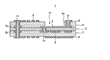
- a multilayer printed wiring board manufactured by this manufacturing method will be described.
- the multilayer printed wiring board 1 has a first wiring pattern 3 formed on one surface 2a of a core substrate 2 serving as a first insulating layer, and has adhesiveness and insulating properties thereon.
- a second insulating layer 4 formed from the first prepreg is laminated, and a second wiring pattern 5 is formed on the second insulating layer 4.
- a third wiring pattern 6 is formed on the other surface 2b of the core substrate 2, and a third insulating layer 7 formed of a second prepreg having adhesiveness and insulating properties is laminated thereon.
- a fourth wiring pattern 8 is formed on the third insulating layer 7.
- vias 2 c that electrically connect the first wiring pattern 3 and the third wiring pattern 6 are formed on the core substrate 2.
- the multilayer printed wiring board 1 includes a via 9, a first wiring pattern 3, a second wiring pattern 5, and a third wiring that electrically connect the first wiring pattern 3 and the second wiring pattern 5.
- a through hole 10 is formed to electrically connect the wiring pattern 6 and the fourth wiring pattern 8.
- the multilayer printed wiring board 1 includes a part of the core substrate 2 and a first portion thereon because the second insulating layer 4 is not laminated on a part including the first wiring pattern 3 on the core substrate 2.
- the exposed pattern 11 is exposed.
- the exposed region 11 has a concave shape. For example, when an electronic component is mounted on the first wiring pattern 3 in the exposed region 11, the height can be reduced. it can.
- Such a multilayer printed wiring board 1 can be manufactured as follows.
- a core substrate 2 provided with copper foil 12 on both sides is prepared.
- the core substrate 2 is excellent in heat resistance, mechanical strength, and electrical characteristics.
- a resin such as polyimide, epoxy resin, phenol resin, or BT resin is used.
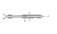
- the first wiring pattern 3, the third wiring pattern 6, and the via 2 c that electrically connects the first wiring pattern 3 and the third wiring pattern 6 are formed.
- a method of forming the via 2c for example, a method of forming a hole in the copper foil 12 and the core substrate 2 where the via 2c is to be formed by laser from the other surface 2b of the core substrate 2 of FIG.
- a through hole may be formed by forming a through hole by a drill or the like and then performing copper plating.
- a resist is formed on the via 2c and the copper foil 12 forming the first wiring pattern 3 so that the formed via 2c is not etched, and the copper foil provided on the one surface 2a of the core substrate 2 is formed. 12 is etched by, for example, a subtractive method to form the first wiring pattern 3.
- the third wiring pattern 6 is formed by etching the copper foil 12 provided on the other surface 2b of the core substrate 2 by, for example, a subtractive method.
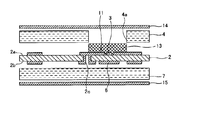
- an alkali-soluble ink is applied to the exposed region 11 exposing the first wiring pattern 3 to form an ink layer 13.
- the ink layer 13 is formed by printing an alkali-soluble ink on the exposed region 11 by a printing method such as screen printing or ink jet printing, and drying and curing under appropriate conditions.
- the entire ink layer is cured by three-dimensional crosslinking.
- the ink is alkali-soluble means that the ink is soluble in an alkaline solution not only before curing but also after curing, preferably because the ink after curing develops a dry film resist. Although it does not melt
- the ink that is soluble in an alkaline solution even after curing includes at least one of tetracarboxylic acid, tetracarboxylic dianhydride, and tetraester dianhydride half-esterified products, and a hydroxyl group in one molecule.
- An ink containing a polyhydric alcohol having 3 or more and a filler can be used.
- at least one of tetracarboxylic acid, tetracarboxylic dianhydride, and a half esterified product of tetracarboxylic dianhydride reacts with a polyhydric alcohol having three or more hydroxyl groups in one molecule.
- the cured product of the ink is soluble in an alkaline solution, has heat resistance, and is very flexible so that even a thick film can be obtained. Bending cracks will not occur. Moreover, by containing the filler, the shape of the layer can be maintained well, and the heat resistance is further improved.
- tetracarboxylic dianhydride any of those generally known as an epoxy curing agent or a raw material for polyimide synthesis can be used.
- examples of tetracarboxylic dianhydride include pyromellitic dianhydride, 3,3,4,4-biphenyltetracarboxylic dianhydride, 3,3,4,4-benzophenone tetracarboxylic dianhydride, Oxy-4,4-diphthalic dianhydride, ethylene bistrimellitic dianhydride, 2,2-bis (4- (3,4-dicarboxyphenoxy) phenyl) propane dianhydride, 1,2,3 4-butanetetracarboxylic dianhydride, 5- (2,5-dioxotetrahydro-3-furanyl) -3-methyl-3-cyclohexene-1,2-dicarboxylic anhydride, and the like. One or a plurality of them can be used in combination.
- tetracarboxylic acid for example, a tetracarboxylic acid capable of forming an acid dianhydride in the molecule is obtained by reacting the above tetracarboxylic dianhydride with water and opening the acid anhydride group. It is done.
- a tetraester dianhydride half-esterified product is obtained by reacting the above tetracarboxylic dianhydride with an alcohol to open the acid anhydride group.
- tetracarboxylic acid, tetracarboxylic dianhydride, and half esterified product of tetracarboxylic dianhydride may be contained in the ink, or one or more of them may be contained.
- the reaction between the acid anhydride and the polyhydric alcohol proceeds even at room temperature, so from the viewpoint of extending the pot life, a half-esterified product of tetracarboxylic acid or tetracarboxylic dianhydride is used.
- a half-esterified product of tetracarboxylic dianhydride is preferable.
- examples of the polyhydric alcohol having three or more hydroxyl groups in one molecule in the ink component include, for example, polyols such as glycerin, diglycerin, polyglycerin, erythritol, pentaerythritol, trimethylolpropane, and ethylene.
- polyols such as glycerin, diglycerin, polyglycerin, erythritol, pentaerythritol, trimethylolpropane, and ethylene.
- Polyether polyols obtained by polymerization addition of alkylene oxides such as oxide and propylene oxide, polyester polyols containing an ester bond with dicarboxylic acid, polycaprolactone polyols obtained by polymerization addition of ⁇ -caprolactone, and the like can be used.
- inorganic materials are preferable, for example, silica, talc, synthetic mica, aluminum hydroxide, magnesium hydroxide, calcium carbonate, magnesium carbonate, aluminum borate, alumina, barium sulfate, magnesium oxide and the like are preferable.
- the ink contains thixotropic agent such as alkali-soluble resin, Aerosil, silicone, fluorine-based leveling agent, antifoaming agent, phthalocyanine blue, phthalocyanine green, titanium oxide and other colorants, Additives such as metal deactivators and antioxidants can also be used as appropriate. Moreover, a solvent can be contained as needed.
- thixotropic agent such as alkali-soluble resin, Aerosil, silicone, fluorine-based leveling agent, antifoaming agent, phthalocyanine blue, phthalocyanine green, titanium oxide and other colorants
- Additives such as metal deactivators and antioxidants can also be used as appropriate.
- a solvent can be contained as needed.
- the ink layer 13 is formed with substantially the same thickness as the first prepreg layer 4 laminated on the first wiring pattern 3 in the next step.
- the first prepreg layer 4 is formed on the surface of the core substrate 2 on the ink layer forming side with the ink layer 13 facing outward. That is, the first prepreg layer 4 is formed so that the ink layer 13 is exposed from the first prepreg layer 4. Specifically, the first prepreg layer 4 is disposed on the portion of the one surface 2 a of the core substrate on which the ink layer 13 is formed, on which the ink layer 13 is not formed, and the first prepreg layer 4 is disposed on the entire other surface 2 b of the core substrate 2. Two prepreg layers 7 are arranged.
- an opening 4 a having a size capable of inserting the ink layer 13 is provided in advance in a mold or the like at a position corresponding to the ink layer 13. It is formed by punching out.
- the resin in the first prepreg layer 4 does not overlap the ink layer 13 even if the resin in the first prepreg layer 4 flows to the ink layer 13 side in the subsequent lamination process.
- the ink layer 13 may be formed larger than the ink layer 13.
- the ink layer 13 is inserted into the opening 4 a and the first prepreg layer 4 is disposed on the first wiring pattern 3.
- a bonding sheet may be used, the insulation board
- the copper foil 14 that becomes the second wiring pattern 5 on the first prepreg layer 4 and the copper foil 15 that becomes the fourth wiring pattern 8 on the second prepreg layer 7. Deploy.
- the copper foil is pasted.
- a coated copper-clad insulating substrate may be used. In this case, an area corresponding to the ink layer 13 of the copper-clad insulating substrate is opened in advance.
- the first prepreg layer 4, the second prepreg layer 7, and the copper foils 14, 15 are arranged and heated toward the core substrate 2 side while being heated with a laminating press, so that the semi-cured first
- the layers are bonded and integrated to form a laminate 16 having a multilayer structure as shown in FIG. .
- the resin constituting the first prepreg layer 4 is exposed by the ink layer 13, preferably by the cured ink layer. 11 can be prevented, and the first wiring pattern 3 to be exposed can be prevented from being attached with resin, and the exposed region 11 can be prevented from being blocked with resin.
- the via 9 forms a hole from the copper foil 14 that forms the second wiring pattern 5 to the first wiring pattern 3 using a drill or by laser processing, and electroless copper plating is performed on the entire surface of the formed hole. It can form by performing the copper plating by the method and the electrolytic copper plating method.
- the through hole 10 forms a through hole that penetrates from the copper foil 14 that forms the second wiring pattern 5 to the copper foil 15 that forms the fourth wiring pattern 8 by using a drill or by laser processing. The burrs remaining in the holes can be removed, and the entire surface of the through holes can be formed by performing copper plating by an electroless copper plating method or an electrolytic copper plating method.
- the second wiring pattern 5 and the fourth wiring pattern 8 are formed by the subtractive method. Specifically, first, dry film resists 17 and 18 are formed on the entire surface of the copper foil 14 and the copper foil 15, and the dry film resists 17 and 18 are exposed using a mask in order to form a desired wiring pattern. . Thereafter, the dry film resist in the unexposed area is dissolved and removed with a solution such as sodium hydrogen carbonate, and then etched by an ordinary method using an iron chloride or copper chloride solution, whereby the second wiring pattern 5 and the fourth wiring pattern. 8 is formed. At the time of etching, the copper foil 14 on the ink layer 13 is dissolved and removed, but the ink layer 13 remains, and the first wiring pattern 3 formed in the exposed region 11 is removed from the wet etching etchant. Can be protected.
- the dry film resists 17 and 18 on the second wiring pattern 5 and the fourth wiring pattern 8 are removed with an alkaline solution such as sodium hydroxide, and the ink layer 13 is also dissolved and removed with the alkaline solution.
- the multilayer printed wiring board 1 of FIG. 1 in which a part of the core substrate 2 and the first wiring pattern 3 are exposed to the outside in the exposed region 11 is obtained. If the ink layer 13 cannot be completely removed in this step, the ink layer 13 may be completely removed by dipping in an alkaline solution. In this way, the ink layer 13 can be easily and completely removed by dissolving and removing the ink layer 13 with an alkaline solution without manually peeling the ink layer 13 or removing it by a physical means. The removal of the dry film resists 17 and 18 and the removal of the ink layer 13 may be performed in separate steps.
- the ink layer 13, preferably the cured ink layer 13, is formed in the exposed region 11 where the first wiring pattern 3 is exposed, the first prepreg layer Even if 4 is heated and pressurized, the resin constituting the first prepreg layer 4 can be prevented from flowing into the exposed region 11, the first wiring pattern 3 can be protected, and an electrical failure occurs. Can be prevented.
- the ink layer 13 is formed from an alkali-soluble ink, the ink layer 13 can be easily and completely removed with an alkaline solution. Therefore, even if the exposed region 11 has a fine shape, the exposed region 11 and the first wiring pattern 3 can be appropriately protected, and the residue of the ink layer 13 can be prevented from occurring in the exposed region 11.
- the end face of the adjacent second insulating layer 4 can be prevented from being damaged or peeled off.
- the end surface of the second insulating layer 4 adjacent to the exposed region 11 on the exposed region 11 side is flat.
- the first wiring pattern 3 is formed in the exposed region 11, so that the exposed region 11 is uneven, and the ink layer 13 is exposed by the lamination press.
- the lamination press When pressed against the concavo-convex surface of the region 11, it is in close contact with the exposed region 11, but can be completely removed by dissolving with an alkaline solution. For this reason, it is possible to prevent the residue of the ink layer 13 from being generated on the first wiring pattern 3 or between the first wiring patterns 3.
- the first wiring pattern 3 in the exposed region 11 is a connection terminal for mounting the electronic component 19.
- the thickness of the multilayer printed wiring board 1 in the exposed region 11 is thinner than the portion where the second wiring pattern 5 is provided, and is formed in a concave shape, so that electrons are formed on the first wiring pattern 3. Even if the component 19 is mounted, the height does not become too high, and the height can be reduced.
- the wiring pattern is provided on both surfaces of the core substrate 2.
- the present invention is not limited to this, and the wiring pattern may be provided only on one surface 2a of the core substrate 2.
- the second insulating layer 4 and the second wiring pattern 5 are formed on the one surface 2 a of the core substrate 2. It is good also as a layer more than a layer.
- an exposed region may be formed on the other surface 2b of the core substrate 2 as shown in FIG. 10 to be described later, and an insulating layer and a wiring pattern may be formed to form three or more layers.
- the core substrate In addition to exposing the wiring pattern on 2, other wiring patterns located inside may be exposed on both surfaces 2 a and 2 b.
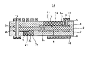
- ink is used to expose not only on one surface 2a side of the core substrate 2 but also on the other surface 2b side as in the multilayer printed wiring board 20 shown in FIG. Region 21 can also be formed.
- this multilayer printed wiring board 20 about the structure similar to the multilayer printed wiring board 1 mentioned above, the same code
- the first wiring pattern 3 is exposed in the exposed region 11 provided on the one surface 2 a side of the core substrate 2, so that the first wiring pattern 3 is exposed, and the core substrate 2 is exposed. Since the third insulating layer 7 is not formed in the exposed region 21 provided on the other surface 2b side, a part of the third wiring pattern 6 is exposed.
- the manufacturing method of the multilayer printed wiring board 20 is similar to the manufacturing method of the multilayer printed wiring board 1 described above.
- an alkali-soluble ink layer 13 is formed on one surface 2a, and an alkali-soluble ink layer 22 is also formed on the other surface 2b.
- the ink layers 13 and 22 are formed with substantially the same thickness as the first prepreg layer 4 serving as the second insulating layer and the second prepreg layer 7 serving as the third insulating layer, respectively.
- the entire 22 is cured.
- 7 is disposed on the first wiring pattern 3 and the third wiring pattern 6 so that the ink layers 13 and 22 face outward, and copper foils 14 and 15 are provided on the prepreg layers 4 and 7, respectively.
- Deploy. And like the manufacturing method of the multilayer printed wiring board 1 mentioned above, it becomes the integrated multilayer laminated body 23 shown in FIG. 12 by heating and pressurizing. At this time, since the ink layers 13 and 22 are formed, it is possible to prevent the resin from flowing into the exposed regions 11 and 21 from the first prepreg layer 4 and the second prepreg layer 7.
- the second wiring pattern 5 and the second wiring pattern 5 are formed by forming the through hole 10 and the via 9 and etching the copper foils 14 and 15 in the same manner as in the method for manufacturing the multilayer printed wiring board 1 described above.
- 4 wiring patterns 8 are formed. Thereafter, when the dry film resists 17 and 18 used in forming the second wiring pattern 5 and the fourth wiring pattern 8 are removed with an alkaline solution, the ink layers 13 and 22 formed in the exposed regions 11 and 21 are removed. Also dissolve and remove. When the second wiring pattern 5 and the fourth wiring pattern 8 are formed, since the ink layers 13 and 22 are formed in the exposed regions 11 and 21, the first exposed in the exposed regions 11 and 21. The wiring pattern 3 and the third wiring pattern 6 can be protected from the etching solution.
- the first wiring pattern 3 is exposed on both the one surface 2a and the other surface 2b of the core substrate 2 by using alkali-soluble ink.
- the exposed region 11 and the exposed region 21 where the third wiring pattern 6 is exposed can be formed simultaneously.
- the same effect as that of the method for manufacturing the multilayer printed wiring board 1 described above is obtained in both the exposed region 11 and the exposed region 21.
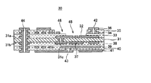
- a multilayer printed wiring board 30 as shown in FIG. 14 can be manufactured using alkali-soluble ink.
- a first wiring pattern 32 is formed on one surface 31a of the core substrate 31 that is a first insulating layer, and the first wiring pattern 32 is protected and adjacent to the first wiring pattern 32.
- the first wiring patterns 32 are insulated from each other, and a second insulating layer 33 having adhesiveness is laminated, and a second wiring pattern 34 is formed on the second insulating layer 33.
- a third insulating layer 35 that protects the pattern 34 and insulates the adjacent second wiring patterns 34 from each other, is laminated, and a third wiring pattern 36 is formed on the third insulating layer 35.
- a fourth wiring pattern 37 is formed on the other surface 31 b of the core substrate 31.
- the fourth insulating layer 38 protects the fourth wiring pattern 37 and insulates the adjacent fourth wiring patterns 37 from each other.
- a fifth wiring pattern 39 is formed on the fourth insulating layer 38 to protect the fifth wiring pattern 39 and to insulate adjacent fifth wiring patterns 39 from each other.
- a layer 40 is laminated, and a sixth wiring pattern 41 is formed on the fifth insulating layer 40.
- the multilayer printed wiring board 30 includes a via 31c that electrically connects the first wiring pattern 32 and the fourth wiring pattern 37 to the core substrate 31, and the second wiring pattern 34 and the third wiring pattern.
- a via 42 electrically connecting 36, a via 43 electrically connecting the fifth wiring pattern 39 and the sixth wiring pattern 41, a first wiring pattern 32, a second wiring pattern 34, and a third wiring pattern.
- Through-holes 44 for electrically connecting the wiring pattern 36, the fourth wiring pattern 37, the fifth wiring pattern 39, and the sixth wiring pattern 41 are formed.
- this multilayer printed wiring board 30 not only a part of the first wiring pattern 32 formed on the core substrate 31 is exposed in the exposed region 45, but also on the second insulating layer 33 in the exposed region 46. A part of the second wiring pattern 34 formed on the outside is also exposed to the outside.
- the multilayer printed wiring board 30 can be manufactured as follows.
- a multilayer printed wiring board having an exposed region 45 is manufactured. Since this can be manufactured in the same manner as the multilayer printed wiring board 1 described above, a detailed description thereof will be omitted.
- alkali-soluble ink is printed on the first exposed region 45 and the second exposed region 46 by screen printing or the like to form an ink layer 47, preferably the ink layer 47. Harden the whole.
- the ink layer 47 is formed on the first exposed region 45 and the second exposed region 46 when the second prepreg layer 35 to be a third insulating layer is heated and pressed in a later step and laminated. This prevents the uncured resin contained in the insulating layer 33 and the resin of the second prepreg layer 35 from flowing in. For this reason, as shown in FIG. 16, the ink layer 47 is a second prepreg layer 35 that is laminated on the second insulating layer 33 in the next step around the opening 33a of the second insulating layer 33. It is formed to have substantially the same thickness as
- the second prepreg layer 35 serving as the third insulating layer is arranged so that the ink layer 47 faces outward. That is, the second prepreg layer 35 is disposed so that the ink layer 47 is exposed from the second prepreg layer. More specifically, the second prepreg layer 35 in which the opening 35a having a size capable of inserting the ink layer 47 is used, and the ink layer 47 is inserted into the opening 35a. To do. Then, a copper foil 48 for forming the third wiring pattern 36 is disposed on the second prepreg layer 35.
- a fourth prepreg layer 40 serving as a fifth insulating layer is disposed, and a copper foil 49 for forming a sixth wiring pattern 41 is disposed thereon.
- the second prepreg layer 35, the fourth prepreg layer 40, and the copper foils 48 and 49 are pressurized while being heated toward the core substrate 31 side, and these are laminated and integrated.
- the ink layer 47 preferably the cured ink layer 47, is formed in the first exposed region 45 and the second exposed region 46, whereby the second insulating layer 33 and the second exposed layer 46 are formed. Even if the prepreg layer 35 is softened, the resin constituting them can be prevented from flowing into the first exposed region 45 and the second exposed region 46, and the first exposed region 45 is formed in the first exposed region 45. It is possible to prevent the resin from attaching to the second wiring pattern 34 formed in the wiring pattern 32 or the second exposed region 46, or blocking the first exposed region 45 and the second exposed region 46 with the resin. .
- vias 42 and 43 and through holes 44 are formed, and the copper foils 48 and 49 are formed on the third wiring pattern 36 and the sixth wiring by a subtractive method.
- a pattern 41 is formed. Since the ink layer 47 remains when the third wiring pattern 36 and the sixth wiring pattern 41 are formed, the first wiring pattern 32 and the second exposure formed in the first exposed region 45. The second wiring pattern 34 formed in the region 46 can be protected from the wet etching solution.
- the dry film resist used in forming the third wiring pattern 36 and the sixth wiring pattern 41 is removed with an alkaline solution such as sodium hydroxide, and the ink layer 47 is also dissolved and removed with the alkaline solution. Then, as shown in FIG. 14, the multilayer printed wiring board 30 in which the first wiring pattern 32 is exposed in the first exposed region 45 and the second wiring pattern 34 is exposed in the second exposed region 46 is obtained. .
- the ink layer 47 is not removed by physical means, but the ink layer 47 is dissolved and removed, so that the first exposed region 45 and the second exposed region are exposed. It is possible to prevent the first wiring pattern 32 and the second wiring pattern 34 exposed in the region 46 from being damaged, and the second insulating layer 33 and the third insulating layer 35 from being peeled off.
- the end surfaces of the second insulating layer 33 and the third insulating layer 35 adjacent to the exposed region 45 and the second exposed region 46 on the first exposed region 45 side and the second exposed region 46 side are flat.
- the first wiring pattern 32 is formed in the first exposed region 45, and the second wiring pattern 34 is formed in the second exposed region 46. Therefore, when the ink layer 47 is pressed against the uneven surfaces of the first exposed region 45 and the second exposed region 46 by the lamination press, the first exposed region 45 and the second exposed region 46 are formed. However, since the ink layer 47 can be completely removed with an alkaline solution, the first wiring pattern 32, the second wiring pattern 34, the first wiring pattern 32, and the second wiring It is possible to prevent the residue of the ink layer 47 from being generated between the patterns 34.
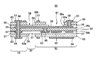
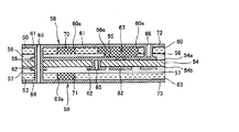
- a method for manufacturing a flex-rigid printed wiring board 50 as shown in FIG. 18 by applying the first and second aspects of the present invention will be described.
- a first rigid portion 52 and a second rigid portion 53 are connected by a flexible flex portion 51.
- the flex portion 51 is a first electrically connecting the first rigid portion 52 and the second rigid portion 53 on one surface 54a of the flexible substrate 54 which is a flexible first insulating layer. Is formed, a first coverlay film 56 is formed to protect the first wiring pattern 55 and to insulate the adjacent first wiring patterns 55 from each other, and a second cover 54b is formed on the other surface 54b.
- the cover lay film 57 is formed.
- the flex portion 51 is a region 58 in which the first coverlay film 56 is exposed by not laminating the first prepreg layer 60 on the first coverlay film 56 on the one surface 54 a side of the flexible substrate 54.
- the second cover lay film 57 is exposed by not laminating the second prepreg layer 63 on the second cover lay film 57 on the other surface 54b side opposite to the region 58.
- the region 59 is made to have.
- the first rigid portion 52 includes a first wiring pattern 55, a first cover lay film 56, a second insulating layer 60 formed of a first prepreg layer, a second surface 54 a of the flexible substrate 54.
- Wiring patterns 61 are laminated.
- the first rigid portion 52 includes a third insulating layer 63 formed of a third wiring pattern 62, a second coverlay film 57, and a second prepreg layer on the other surface 54b of the flexible substrate 54.
- a fourth wiring pattern 64 is laminated.
- the first rigid portion 52 is formed with a via 65 that electrically connects the first wiring pattern 55 and the third wiring pattern 62 to the flexible substrate 54, and the first wiring pattern 55 and the second wiring pattern are formed.
- a via 66 that electrically connects 61 is formed. Further, the first rigid portion 52 has an exposed region 67 that exposes the first wiring pattern 55.
- the second rigid portion 53 includes a first wiring pattern 55, a first coverlay film 56, and a first prepreg layer on one surface 54 a of the flexible substrate 54.
- the formed second insulating layer 60 and the second wiring pattern 61 are laminated, and the third wiring pattern 62, the second coverlay film 57, and the second prepreg layer are formed on the other surface 54b. Further, a third insulating layer 63 and a fourth wiring pattern 64 are laminated.
- the second rigid portion 53 is formed with a through hole 68 that electrically connects the first wiring pattern 55, the second wiring pattern 61, the third wiring pattern 62, and the fourth wiring pattern 64. .
- This flex-rigid printed wiring board 50 can be manufactured as follows. First, as shown in FIG. 19, a flexible substrate having copper foil on both sides is prepared and vias 65 are formed in the same manner as in the method for manufacturing the multilayer printed wiring board 1 described above. A first wiring pattern 55 is formed on 54a by a subtractive method, and a third wiring pattern 62 is formed on the other surface 54b.
- a first coverlay film 56 having an opening 56a formed in a region corresponding to the exposed region 67 is laminated on one surface 54a by a press or the like.
- the second coverlay film 57 is also laminated by pressing or the like.
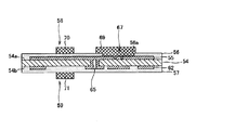
- an alkali-soluble second ink layer 70 having a thickness substantially the same as the thickness of the first prepreg layer 60 laminated on the first coverlay film 56 is formed by screen printing or the like.
- a second prepreg layer 63 that is laminated on the second cover lay film 57 in a later step in a region corresponding to the region 59 where the second prepreg layer 63 is not laminated.
- the alkali-soluble third ink layer 71 is formed with substantially the same thickness as the above.
- the ink layers 69, 70, 71 are cured as a whole.
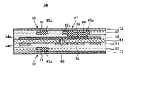
- the first prepreg layer 60 is disposed on the first coverlay film 56 with the first ink layer 69 and the second ink layer 70 facing outward. That is, the first prepreg layer 60 is disposed on the first cover lay film 56 so that the first ink layer 69 and the second ink layer 70 are exposed from the first prepreg layer 60. More specifically, the first prepreg layer 60 in which openings 60 a and 60 b are formed at positions corresponding to the first ink layer 69 and the second ink layer 70 is disposed on the first coverlay film 56. To do.
- the second prepreg layer 63 having an opening 63a formed at a position corresponding to the third ink layer 71 is disposed, whereby the third ink layer 71 is disposed.
- a second prepreg layer 63 facing outward is formed.
- a copper foil 72 for forming the second wiring pattern 61 is disposed on the first prepreg layer 60, the first ink layer 69, and the second ink layer 70, and the second prepreg layer 63, the third A copper foil 73 for forming a fourth wiring pattern 64 is disposed on the ink layer 71.
- the first ink layer 69, the second ink layer 70, and the third ink are used.
- the layer 71 can prevent the resin constituting the first prepreg layer 60 and the second prepreg layer 63 from flowing into the regions 58 and 59 and the exposed region 67, and the resin is attached to the exposed first wiring pattern 55. Further, it is possible to prevent the regions 58 and 59 where the prepreg layer is not laminated and the exposed region 67 from being blocked with resin.
- vias 66 and through holes 68 are formed in the multilayer body 74 as in the case of the vias 9 and the through holes 10 of the multilayer printed wiring board 1 described above.
- the copper foil 72 is etched by the subtractive method to form the second wiring pattern 61, and the copper foil 73 is also etched by the subtractive method to form the fourth wiring pattern 64.
- the first ink layer 69 is formed in the exposed region 67, thereby protecting the first wiring pattern 55 exposed in the exposed region 67 from the etching solution. be able to.
- the resists 75 and 76 used for forming the second wiring pattern 61 and the fourth wiring pattern 64 are removed with an alkaline solution
- the third ink layer 71 is also dissolved and removed with an alkaline solution.
- the first ink layer 69 is formed in the exposed region 67 exposing the first wiring pattern 55 using ink.
- the second ink layer 70 is formed in the region 58 where the first coverlay film 56 is exposed without laminating the first prepreg layer 60.
- the third ink layer 71 is formed in the region 59 where the second coverlay film 57 is exposed without laminating the second prepreg layer 63. Then, the first ink layer 69, the second ink layer 70, and the third ink layer 71 are dissolved and removed with an alkaline solution, thereby exposing the first wiring pattern 55 formed therein in the exposed region 67.
- this exposed region 67 can be used as a connection terminal for an electronic component. Further, since the prepreg layer is not formed in the flex portion 51, flexibility is maintained, and the first wiring pattern 55 is covered with the first cover lay film 56 and the second cover lay film 57.
- the flex part 51 can function as a cable.
- the first prepreg layer 60 and the first prepreg layer 60 are formed when the laminate 74 is formed by forming the second ink layer 70 and the third ink layer 71. Even if the second prepreg layer 63 is heated and pressurized, the resin constituting the first prepreg layer 60 and the second prepreg layer 63 can be prevented from flowing into the region 58 and the region 59. The flexibility of the flexible substrate 54 can be maintained well. Further, by forming the first ink layer 69, it is possible to prevent the resin of the first prepreg layer 60 from flowing into the exposed region 67 when the stacked body 74 is formed. Accordingly, in the exposed region 67, it is possible to prevent the resin from adhering to the exposed first wiring pattern 55, thereby preventing an electrical failure.
- the first ink layer 69, the second ink layer 70, and the third ink layer 71 are not removed by physical means but dissolved by an alkaline solution. Therefore, the first wiring pattern 55 exposed in the exposed region 67 of the first rigid portion 52 is damaged, or the first coverlay film 56, the second coverlay film 57, and the first The first ink layer 69, the second ink layer 70, and the third ink layer 71 can be removed without the prepreg layer 60 and the second prepreg layer 63 being peeled off.
- the first ink layer 69 is pressed against the uneven surface of the exposed region 67 by a lamination press. Then, the first ink layer 69 adheres to the exposed region 67, but the first ink layer 69 can be completely removed by dissolving with an alkaline solution. In addition, poor connection due to the residue of the first ink layer 69 occurring between the first wiring patterns 55 can be prevented.
- the second ink layer 70 and the third ink layer 71 are also dissolved and removed with an alkaline solution, residues of the second ink layer 70 and the third ink layer 71 are generated in the regions 58 and 59. Therefore, it is possible to prevent a decrease in flexibility at the flex part 51.
- an exposed region 67 where the first wiring pattern 55 is exposed is formed in the first rigid portion 52, but the exposed region 67 is formed in the first rigid portion 52.
- an exposed region where the third wiring pattern 62 is exposed is also formed on the other surface 54b of the flexible substrate 54 in the same manner as the multilayer printed wiring board 20 shown in FIG. May be.
- a multilayer printed wiring board 80 as shown in FIG. 26 can be manufactured using alkali-soluble ink.
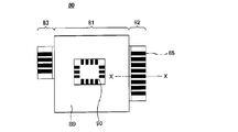
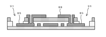
- the multilayer printed wiring board 80 includes a rigid portion 81 on which electronic components and the like are mounted, and flexible terminal portions 82 and 83 provided so as to protrude from two sides of the rigid portion 81.
- the multilayer printed wiring board 80 electrically connects the flexible terminal portions 82 and 83 to connectors of other electronic components, and electrically connects the electronic components mounted on the rigid portion 81 and other electronic components. .
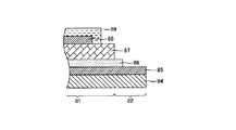
- FIG. 27 shows a cross section taken along line XX in FIG. 26.
- the first wiring pattern 85 is formed on the flexible substrate 84, and the first wiring pattern 85 is formed on the flexible substrate 84.
- a cover lay film 86 that protects one wiring pattern 85 and insulates the first wiring patterns 85 is laminated, and an insulating layer 87 formed of a prepreg layer is formed on the cover lay film 86, and further thereon
- a second wiring pattern 88 is formed.
- the surface of the rigid portion 81 is covered with a solder resist 89 except for the electronic component mounting region 90 where the second wiring pattern 88 is exposed as a terminal.
- a first wiring pattern 85 is formed on the flexible substrate 84.
- the coverlay film 86 and the insulating layer 87 are not laminated on the first wiring pattern 85, and the flexible terminal portions 82 and 83 have portions where the first wiring pattern 85 is exposed.
- the first wiring pattern 85 and the second wiring pattern 88 need to be electrically connected by through holes or vias, but are omitted here.
- the flexible terminal portion 83 is the same as the flexible terminal portion 82 and is not shown.
- the exposed region 91 of the first wiring pattern 85 extends not only to the product portion 92 but also to the product exterior 93, as shown in FIG. It can be formed by punching with ZZ in the drawing as a cut surface.
- the structure of FIG. 28 can be manufactured by the same method as that for forming the exposed region 67 described in the fourth embodiment, and the same effect can be obtained.
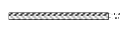
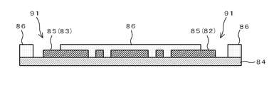
- the multilayer printed wiring board 80 shown in FIG. 26 can be manufactured as follows. First, as shown in FIG. 29, a flexible substrate 84 having a copper foil 100 on one side is prepared, and as shown in FIG. 30, a first wiring pattern 85 is formed by a subtractive method using the copper foil 100. Next, as shown in FIG. 31, a cover lay film 86 in which openings are formed in regions corresponding to the exposed regions 91 and 91 that finally become the flexible terminal portions 82 and 83 is laminated by a press or the like.
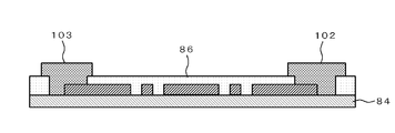
- the alkali-soluble first ink layer 102 and the second ink layer so as to cover the opening portion of the cover lay film 86 (the portion to be the flexible terminal portions 82 and 83) and the periphery thereof.
- the ink layer 103 is formed by screen printing or the like.
- the first ink layer 102 and the second ink layer 103 are substantially the same as the thickness of the prepreg layer 101 that is laminated on the coverlay film 86 in the next step and becomes the insulating layer 87. Form and preferably harden the whole.
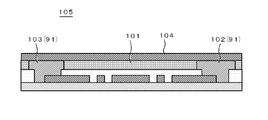
- the prepreg layer 101 is disposed on the cover lay film 86 with the first ink layer 102 and the second ink layer 103 facing outward. That is, the prepreg layer 101 is disposed on the cover lay film 86 so that the first ink layer 102 and the second ink layer 103 are exposed from the prepreg layer 101.
- a copper foil 104 for forming the second wiring pattern 88 is disposed on the prepreg layer 101, the first ink layer 102, and the second ink layer 103.
- vias 106 are formed in the laminate 105 as shown in FIG. 35 in the same manner as the vias 9 of the multilayer printed wiring board 1 of FIG. 1 described above.
- the first wiring pattern 85 and the copper foil 104 on which the second wiring pattern 88 will be formed later are electrically connected.
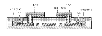
- the copper foil 104 is etched by a subtractive method using a resist 107 to form a second wiring pattern 88.
- the first wiring pattern 85 protruding into the exposed region 91 is formed by forming the first ink layer 102 and the second ink layer 103 in the exposed region 91. Can be protected from the etching solution.
- the resist 107 used for forming the second wiring pattern 88 is removed with an alkaline solution, and the first ink layer 102 and the second ink layer 103 are dissolved and removed with the alkaline solution.
- the first wiring pattern 85 becomes a wiring board exposed in the exposed region 91 as shown in FIG.
- solder resist 89 As a method for forming the solder resist 89, a method in which the solder resist material is directly covered except for the electronic component mounting region 90 by screen printing and then cured by UV (ultraviolet light) or heating, or the solder resist material is coated or screened. After forming on the entire surface by printing or the like, UV light is irradiated outside the electronic component mounting region 90 using a mask or the like to cure, and then the UV unirradiated portion is removed with an alkali solution such as sodium carbonate, and then heated. Furthermore, the method of hardening is mentioned.
- the solder resist 89 After the solder resist 89 is formed, gold plating or the like is applied as necessary. Then, as shown in FIG. 39, the outer part 93 of the product is made of gold with the cut surfaces Z 1 -Z 1 and Z 2 -Z 2 in the drawing.
- the multilayer printed wiring board 80 shown in FIGS. 26 to 28 is completed by punching with a mold or the like.
- the multilayer printed wiring board manufactured by the method of the present invention may further be a wiring board having a plurality of rigid portions and connected between the rigid portions by flex cable portions.
- a multilayer printed wiring board was produced as follows. First, a double-sided copper-clad flexible substrate having a copper foil with a thickness of 18 ⁇ m on both sides of a polyimide insulating layer was prepared, and a wiring pattern was formed on both sides by a normal subtractive method. Next, a coverlay film having a 12.5 ⁇ m-thick polyimide film and an adhesive layer of 25 ⁇ m in which a region corresponding to an exposed region exposing the wiring pattern is previously punched on both surfaces of the flexible substrate and being exposed to vacuum in vacuum. The inner layer substrate was produced by coating by hot pressing.
- an alkali-soluble ink (trade name: SER-451B, manufactured by Yamaei Chemical Co., Ltd.) is printed on the exposed area of the wiring pattern by screen printing, and dried and cured at 150 ° C. for 20 minutes to form an ink layer. did.
- the thickness of the printed film (ink layer) after drying and curing was set to 60 ⁇ m.
- the copper foil was laid up and pressed in a vacuum at 40 ° C./cm 2 at 180 ° C. for 90 minutes to form a laminate.
- the appearance of the laminate after pressing was flat.
- a dry film resist was laminated on the copper foil provided on the outer layer of the laminate, exposed, developed, and etched by spraying with an aqueous iron chloride solution to form a wiring pattern on the copper foil.
- the ink layer remained even after the copper foil corresponding to the unexposed portion of the dry film resist was completely etched away.
- the laminate was immersed in a 3 wt% aqueous sodium hydroxide solution set at 50 ° C. As a result, the ink layer was dissolved and removed, and an internal wiring pattern appeared.
- the multilayer printed wiring was the same as the example except that the ink layer was formed using an ink (trade name: Solder Shield SSZ-100SCB) manufactured by Taiyo Ink Manufacturing Co., Ltd. instead of the alkali-soluble ink. A plate was made.
- an ink trade name: Solder Shield SSZ-100SCB
- the ink is not alkali-soluble, the ink layer was not removed and the internal wiring pattern did not appear.
- the ink layer was carefully peeled by hand, the ink layer digged into the prepreg, and an ink layer residue was formed at the boundary with the prepreg ink.
- a part of the prepreg was taken together with the peeled ink layer, and the prepreg was cracked.
- residue was observed between the wiring patterns.
- multilayer printed wiring boards such as flex-rigid multilayer wiring boards and rigid multilayer wiring boards that expose a part of the inner layer area such as the wiring pattern or the inner layer area that functions as a cable. .
Landscapes
- Engineering & Computer Science (AREA)
- Manufacturing & Machinery (AREA)
- Microelectronics & Electronic Packaging (AREA)
- Production Of Multi-Layered Print Wiring Board (AREA)
Abstract
Description
第1の絶縁層上の上記配線パターンを含む一部にアルカリ可溶性のインク層を形成し、
第1の絶縁層上のインク層形成側の面に第2の絶縁層を、該第2の絶縁層から上記インク層が露出するように形成するとともに、該第2の絶縁層上に金属層を形成し、
上記金属層をパターニングして第2の配線パターンを形成した後、上記インク層をアルカリ溶液で溶解して除去し、第1の絶縁層の一部とその上の配線パターンとを露出させることを特徴とする。
上記第1の絶縁層の配線パターン形成面にカバーレイを配置し、
該カバーレイ上の一部にアルカリ可溶性のインク層を形成し、
上記カバーレイ上に第2の絶縁層を、該第2の絶縁層から上記インク層が露出するように形成すると共に、該第2の絶縁層上に金属層を形成し、
上記金属層をパターニングして配線パターンを形成した後、上記インク層をアルカリ溶液で溶解して除去し、カバーレイの一部を露出させることを特徴とする。
〈実施例〉
実施例では、次のようにして多層プリント配線板を作製した。先ず、ポリイミド絶縁層の両面に厚み18μmの銅箔を有する両面銅貼りフレキシブル基板を用意し、その両面に通常のサブトラクティブ法により配線パターンを形成した。次に、フレキシブル基板の両面に、予め、配線パターンを露出させる露出領域と対応する領域を打ち抜きにより開口した12.5μm厚のポリイミドフィルムと25μmの接着剤層を有するカバーレイフィルムを真空中にて熱プレスして被覆し、内層基板を作製した。次に、配線パターンの露出領域にスクリーン印刷により、アルカリ可溶性インク(山栄化学株式会社製、商品名:SER-451B)を印刷し、150℃、20分間、乾燥及び硬化してインク層を形成した。乾燥、硬化後の印刷膜(インク層)の厚みは、60μmとなるようにした。
比較例では、アルカリ可溶性インクに代えて、太陽インキ製造株式会社製のインク(商品名:ソルダーシールドSSZ-100SCB)を用いてインク層を形成したこと以外は、実施例と同様にして多層プリント配線板を作製した。
2 第1の絶縁層(コア基板)
2a コア基板の一方の面
2b コア基板の他方の面
2c ビア
3 第1の配線パターン
4 第2の絶縁層(第1のプリプレグ層)
4a 第1のプリプレグ層の開口部
5 第2の配線パターン
6 第3の配線パターン
7 第3の絶縁層(第2のプリプレグ層)
7a 第2のプリプレグ層の開口部
8 第4の配線パターン
9 ビア
10 スルーホール
11 露出領域
12 銅箔
13 インク層
14 銅箔
15 銅箔
16 積層体
17 ドライフィルムレジスト
18 ドライフィルムレジスト
19 電子部品
20 多層プリント配線板
21 露出領域
22 インク層
23 多層積層体
30 多層プリント配線板
31 第1の絶縁層(コア基板)
31a コア基板の一方の面
31b コア基板の他方の面
31c ビア
32 第1の配線パターン
33 第2の絶縁層(第1のプリプレグ層)
33a 第1のプリプレグ層の開口部
34 第2の配線パターン
35 第3の絶縁層(第2のプリプレグ層)
35a 第2のプリプレグ層の開口部
36 第3の配線パターン
37 第4の配線パターン
38 第4の絶縁層(第3のプリプレグ層)
39 第5の配線パターン
40 第5の絶縁層(第4のプリプレグ層)
41 第6の配線パターン
42 ビア
43 ビア
44 スルーホール
45 第1の露出領域
46 第2の露出領域
47 インク層
48 銅箔
49 銅箔
50 フレックスリジッドプリント配線板
51 フレックスリジッドプリント配線板50のフレックス部
52 フレックスリジッドプリント配線板50の第1のリジッド部
53 フレックスリジッドプリント配線板50の第2のリジッド部
54 第1の絶縁層(フレキシブル基板)
54a フレキシブル基板の一方の面
54b フレキシブル基板の他方の面
55 第1の配線パターン
56 第1のカバーレイフィルム
56a 第1のカバーレイフィルムの開口部
57 第2のカバーレイフィルム
58 領域
59 領域
60 第2の絶縁層(第1のプリプレグ層)
60a 第1のプリプレグ層の開口部
60b 第1のプリプレグ層の開口部
60c 第1のプリプレグ層の開口部
61 第2の配線パターン
62 第3の配線パターン
63 第3の絶縁層(第2のプリプレグ層)
64 第4の配線パターン
65 ビア
66 ビア
67 露出領域
68 スルーホール
69 第1のインク層
70 第2のインク層
71 第3のインク層
72 銅箔
73 銅箔
74 積層体
75 レジスト
76 レジスト
80 多層プリント配線板
81 多層プリント配線板80のリジッド部
82 多層プリント配線板80のフレキ端子部
83 多層プリント配線板80のフレキ端子部
84 フレキシブル基板
85 第1の配線パターン
86 カバーレイフィルム
87 絶縁層
88 第2の配線パターン
89 ソルダーレジスト
90 電子部品実装領域
91 露出領域
92 製品部
93 製品外部
100 銅箔
101 プリプレグ層
102 第1のインク層
103 第2のインク層
104 銅箔
105 積層体
106 ビア
107 レジスト
Claims (16)
- 第1の絶縁層の少なくとも片面に配線パターンを形成し、
第1の絶縁層上の上記配線パターンを含む一部にアルカリ可溶性のインク層を形成し、
第1の絶縁層上のインク層形成側の面に第2の絶縁層を、該第2の絶縁層から上記インク層が露出するように形成するとともに、該第2の絶縁層上に金属層を形成し、
上記金属層をパターニングして第2の配線パターンを形成した後、上記インク層をアルカリ溶液で溶解して除去し、第1の絶縁層の一部とその上の配線パターンとを露出させることを特徴とする多層プリント配線板の製造方法。 - インク層の形成において、インク層全体を硬化させる請求項1記載の多層プリント配線板の製造方法。
- 上記第2の配線パターンを形成するために該第2の絶縁層上に設けたレジストと、上記インク層とを上記アルカリ溶液で同時に除去する請求項1記載の多層プリント配線板の製造方法。
- 上記第2の絶縁層及び上記金属層は、上記第1の絶縁層上のインク層形成側の面に該インク層が露出するように配置したプリプレグと、該プリプレグ上に配置した金属箔とを加熱しながら加圧することにより積層一体化させることで形成する請求項1記載の多層プリント配線板の製造方法。
- 上記第2の絶縁層及び上記金属層は、上記第1の絶縁層のインク形成面に、金属箔が貼着された絶縁基板を上記インク層が露出するように配置し、加熱しながら加圧することにより積層一体化させることで形成する請求項1記載の多層プリント配線板の製造方法。
- 上記第1の絶縁層の両面において、請求項1記載の方法により第1の絶縁層の一部とその上の配線パターンを露出させる多層プリント配線板の製造方法。
- 上記第2の配線パターンが形成された第2の絶縁層上に、さらに絶縁層及び配線パターンを順次形成して多層構造を形成する多層プリント配線板の製造方法であって、
第2の絶縁層上の第2の配線パターンを含む一部にアルカリ可溶性の新たなインク層を形成し、
第2の絶縁層上に新たな絶縁層を、該新たな絶縁層から上記新たなインク層が露出するように形成するとともに、該新たな絶縁層上に新たな金属層を形成し、
該新たな金属層をパターニングして新たな配線パターンを形成し、上記新たなインク層をアルカリ溶液で溶解して除去し、第2の絶縁層の一部とその上の第2の配線パターンとを露出させる請求項1記載の多層プリント配線板の製造方法。 - 上記第1の絶縁層が可撓性を有し、
上記第1の絶縁層上の配線パターンの形成後、上記インク層の形成前に、第1の絶縁層及び配線パターンの露出させる部分を除いて第1の絶縁層上をカバーレイで被覆する請求項1記載の多層プリント配線板の製造方法。 - 上記カバーレイ上の一部に第2のインク層を形成し、上記第2の絶縁層を、該第2の絶縁層から第1の絶縁層上のインク層と共に第2のインク層が露出するように形成し、上記アルカリ溶液で第1の絶縁層上のインク層と共にカバーレイ上の第2のインク層を溶解して除去し、カバーレイの一部を露出させる請求項8記載の多層プリント配線板の製造方法。
- 第1の絶縁層の両側で、カバーレイの露出させる部分をそれら対向するように形成する請求項9記載の多層プリント配線板の製造方法。
- 上記第1の絶縁層上の露出した配線パターンを電子部品の接続端子とする請求項1記載の多層プリント配線板の製造方法。
- インク層の除去により露出した第1の絶縁層を切断する請求項8記載の多層プリント配線板の製造方法。
- 第1の絶縁層上の露出した配線パターンを電子部品の接続端子とする請求項12記載の多層プリント配線板の製造方法。
- 可撓性を有する第1の絶縁層の少なくとも片面に配線パターンを形成し、
上記第1の絶縁層の配線パターン形成面にカバーレイを配置し、
該カバーレイ上の一部にアルカリ可溶性のインク層を形成し、
上記カバーレイ上に第2の絶縁層を、該第2の絶縁層から上記インク層が露出するように形成すると共に、該第2の絶縁層上に金属層を形成し、
上記金属層をパターニングして配線パターンを形成した後、上記インク層をアルカリ溶液で溶解して除去し、カバーレイの一部を露出させる多層プリント配線板の製造方法。 - インク層の形成において、インク層全体を硬化させる請求項14記載の多層プリント配線板の製造方法。
- 第1の絶縁層の両面において、カバーレイの露出させる部分をそれらが対向するように形成する請求項15記載の多層プリント配線板の製造方法。
Priority Applications (4)
| Application Number | Priority Date | Filing Date | Title |
|---|---|---|---|
| CN2009801596669A CN102461350A (zh) | 2009-06-02 | 2009-06-02 | 多层印刷布线板的制造方法 |
| PCT/JP2009/060058 WO2010140214A1 (ja) | 2009-06-02 | 2009-06-02 | 多層プリント配線板の製造方法 |
| JP2010513557A JPWO2010140214A1 (ja) | 2009-06-02 | 2009-06-02 | 多層プリント配線板の製造方法 |
| TW098119161A TW201044939A (en) | 2009-06-02 | 2009-06-09 | Method for manufacturing multilayer printed wiring board |
Applications Claiming Priority (1)
| Application Number | Priority Date | Filing Date | Title |
|---|---|---|---|
| PCT/JP2009/060058 WO2010140214A1 (ja) | 2009-06-02 | 2009-06-02 | 多層プリント配線板の製造方法 |
Publications (1)
| Publication Number | Publication Date |
|---|---|
| WO2010140214A1 true WO2010140214A1 (ja) | 2010-12-09 |
Family
ID=43297360
Family Applications (1)
| Application Number | Title | Priority Date | Filing Date |
|---|---|---|---|
| PCT/JP2009/060058 Ceased WO2010140214A1 (ja) | 2009-06-02 | 2009-06-02 | 多層プリント配線板の製造方法 |
Country Status (4)
| Country | Link |
|---|---|
| JP (1) | JPWO2010140214A1 (ja) |
| CN (1) | CN102461350A (ja) |
| TW (1) | TW201044939A (ja) |
| WO (1) | WO2010140214A1 (ja) |
Cited By (8)
| Publication number | Priority date | Publication date | Assignee | Title |
|---|---|---|---|---|
| CN102638947A (zh) * | 2012-04-24 | 2012-08-15 | 杭州新三联电子有限公司 | 银浆跨线印制线路板生产工艺 |
| CN103547072A (zh) * | 2012-07-12 | 2014-01-29 | Si弗莱克斯有限公司 | 形成有刚性区域和柔性区域的印刷电路板的冲压工艺方法 |
| GB2510956A (en) * | 2012-12-11 | 2014-08-20 | Intel Corp | Recessed discrete component mounting on organic substrate |
| JP2015090931A (ja) * | 2013-11-06 | 2015-05-11 | 太陽誘電株式会社 | 複合基板及びリジッド基板 |
| JP2018060914A (ja) * | 2016-10-05 | 2018-04-12 | パナソニックIpマネジメント株式会社 | 多層プリント配線板、多層プリント配線板の製造方法 |
| JP2018160708A (ja) * | 2018-07-23 | 2018-10-11 | 太陽誘電株式会社 | 複合基板及びリジッド基板 |
| JP2019016665A (ja) * | 2017-07-05 | 2019-01-31 | 株式会社フジクラ | 多層プリント配線板の製造方法 |
| JP2021526736A (ja) * | 2018-07-19 | 2021-10-07 | ステムコ カンパニー リミテッド | 多層回路基板およびその製造方法 |
Families Citing this family (4)
| Publication number | Priority date | Publication date | Assignee | Title |
|---|---|---|---|---|
| KR102466204B1 (ko) * | 2015-12-16 | 2022-11-11 | 삼성전기주식회사 | 인쇄회로기판 및 인쇄회로기판의 제조방법 |
| KR102501905B1 (ko) * | 2017-11-09 | 2023-02-21 | 삼성전기주식회사 | 인쇄회로기판 및 그 제조방법 |
| CN113840450B (zh) * | 2021-09-30 | 2024-01-30 | 昆山国显光电有限公司 | 印刷电路板 |
| TWI823523B (zh) * | 2022-08-17 | 2023-11-21 | 先豐通訊股份有限公司 | 電路板及其製作方法 |
Citations (9)
| Publication number | Priority date | Publication date | Assignee | Title |
|---|---|---|---|---|
| JPH0239594A (ja) * | 1988-07-29 | 1990-02-08 | Sharp Corp | リジッドフレキシブル配線板の製造方法 |
| JPH06204663A (ja) * | 1993-01-05 | 1994-07-22 | Toshiba Corp | プリント配線板の製造方法 |
| JPH08174755A (ja) * | 1994-12-21 | 1996-07-09 | Toagosei Co Ltd | 銅張絶縁シートおよび多層プリント配線板の製造方法 |
| JPH09283932A (ja) * | 1996-04-08 | 1997-10-31 | Ibiden Co Ltd | 多層プリント配線板の製造方法 |
| JPH10107439A (ja) * | 1996-09-27 | 1998-04-24 | Kyocera Corp | 積層セラミック基板の製造方法 |
| JPH10126056A (ja) * | 1996-10-18 | 1998-05-15 | Victor Co Of Japan Ltd | プリント配線基板の製造方法 |
| JP2001015917A (ja) * | 1999-06-30 | 2001-01-19 | Toshiba Corp | リジッドフレックスプリント配線板の製造方法 |
| JP2006203155A (ja) * | 2005-01-20 | 2006-08-03 | Samsung Electro Mech Co Ltd | リジッドフレキシブルプリント基板の製造方法 |
| JP2007088477A (ja) * | 2005-09-22 | 2007-04-05 | Samsung Electro-Mechanics Co Ltd | キャビティを備えた基板の製造方法 |
-
2009
- 2009-06-02 CN CN2009801596669A patent/CN102461350A/zh active Pending
- 2009-06-02 WO PCT/JP2009/060058 patent/WO2010140214A1/ja not_active Ceased
- 2009-06-02 JP JP2010513557A patent/JPWO2010140214A1/ja active Pending
- 2009-06-09 TW TW098119161A patent/TW201044939A/zh unknown
Patent Citations (9)
| Publication number | Priority date | Publication date | Assignee | Title |
|---|---|---|---|---|
| JPH0239594A (ja) * | 1988-07-29 | 1990-02-08 | Sharp Corp | リジッドフレキシブル配線板の製造方法 |
| JPH06204663A (ja) * | 1993-01-05 | 1994-07-22 | Toshiba Corp | プリント配線板の製造方法 |
| JPH08174755A (ja) * | 1994-12-21 | 1996-07-09 | Toagosei Co Ltd | 銅張絶縁シートおよび多層プリント配線板の製造方法 |
| JPH09283932A (ja) * | 1996-04-08 | 1997-10-31 | Ibiden Co Ltd | 多層プリント配線板の製造方法 |
| JPH10107439A (ja) * | 1996-09-27 | 1998-04-24 | Kyocera Corp | 積層セラミック基板の製造方法 |
| JPH10126056A (ja) * | 1996-10-18 | 1998-05-15 | Victor Co Of Japan Ltd | プリント配線基板の製造方法 |
| JP2001015917A (ja) * | 1999-06-30 | 2001-01-19 | Toshiba Corp | リジッドフレックスプリント配線板の製造方法 |
| JP2006203155A (ja) * | 2005-01-20 | 2006-08-03 | Samsung Electro Mech Co Ltd | リジッドフレキシブルプリント基板の製造方法 |
| JP2007088477A (ja) * | 2005-09-22 | 2007-04-05 | Samsung Electro-Mechanics Co Ltd | キャビティを備えた基板の製造方法 |
Cited By (13)
| Publication number | Priority date | Publication date | Assignee | Title |
|---|---|---|---|---|
| CN102638947A (zh) * | 2012-04-24 | 2012-08-15 | 杭州新三联电子有限公司 | 银浆跨线印制线路板生产工艺 |
| CN103547072A (zh) * | 2012-07-12 | 2014-01-29 | Si弗莱克斯有限公司 | 形成有刚性区域和柔性区域的印刷电路板的冲压工艺方法 |
| GB2510956A (en) * | 2012-12-11 | 2014-08-20 | Intel Corp | Recessed discrete component mounting on organic substrate |
| GB2510956B (en) * | 2012-12-11 | 2016-03-09 | Intel Corp | Recessed discrete component mounting on organic substrate |
| JP2015090931A (ja) * | 2013-11-06 | 2015-05-11 | 太陽誘電株式会社 | 複合基板及びリジッド基板 |
| WO2018066213A1 (ja) * | 2016-10-05 | 2018-04-12 | パナソニックIpマネジメント株式会社 | 多層プリント配線板、多層プリント配線板の製造方法 |
| JP2018060914A (ja) * | 2016-10-05 | 2018-04-12 | パナソニックIpマネジメント株式会社 | 多層プリント配線板、多層プリント配線板の製造方法 |
| US10785868B2 (en) | 2016-10-05 | 2020-09-22 | Panasonic Intellectual Property Management Co., Ltd. | Multilayer printed wiring board and method for producing multilayer printed wiring board |
| TWI715794B (zh) * | 2016-10-05 | 2021-01-11 | 日商松下知識產權經營股份有限公司 | 多層印刷配線板、多層印刷配線板之製造方法 |
| JP2019016665A (ja) * | 2017-07-05 | 2019-01-31 | 株式会社フジクラ | 多層プリント配線板の製造方法 |
| JP2021526736A (ja) * | 2018-07-19 | 2021-10-07 | ステムコ カンパニー リミテッド | 多層回路基板およびその製造方法 |
| JP7136930B2 (ja) | 2018-07-19 | 2022-09-13 | ステムコ カンパニー リミテッド | 多層回路基板およびその製造方法 |
| JP2018160708A (ja) * | 2018-07-23 | 2018-10-11 | 太陽誘電株式会社 | 複合基板及びリジッド基板 |
Also Published As
| Publication number | Publication date |
|---|---|
| CN102461350A (zh) | 2012-05-16 |
| JPWO2010140214A1 (ja) | 2012-11-15 |
| TW201044939A (en) | 2010-12-16 |
Similar Documents
| Publication | Publication Date | Title |
|---|---|---|
| WO2010140214A1 (ja) | 多層プリント配線板の製造方法 | |
| JPWO2009069683A1 (ja) | 多層プリント配線板の製造方法 | |
| US7082679B2 (en) | Rigid-flexible PCB having coverlay made of liquid crystalline polymer and fabrication method thereof | |
| JP5526746B2 (ja) | 多層基板の製造方法及び支持基板 | |
| KR101462724B1 (ko) | 리지드 플렉시블 인쇄회로기판 제조방법 | |
| JP2006203155A (ja) | リジッドフレキシブルプリント基板の製造方法 | |
| WO2009099065A1 (ja) | レジストインク及び多層プリント配線板の製造方法 | |
| JP2011061176A (ja) | プリント基板の製造方法 | |
| TW201334647A (zh) | 多層配線基板及其製造方法 | |
| TW200412205A (en) | Double-sided printed circuit board without via holes and method of fabricating the same | |
| JP4520392B2 (ja) | プリント基板の製造方法 | |
| JP2013187255A (ja) | 配線基板の製造方法 | |
| TWI693004B (zh) | 軟硬結合板及其製作方法 | |
| US9237656B2 (en) | Method of manufacturing multi-layer wiring board | |
| WO2017159773A1 (ja) | フレキシブル回路基板およびその製造方法 | |
| WO2009136603A1 (ja) | フレックスリジッド配線基板とその製造方法 | |
| JP2010278261A (ja) | 多層プリント配線板の製造方法 | |
| JP2013123035A (ja) | 多層配線基板の製造方法 | |
| KR100905574B1 (ko) | 인쇄회로기판의 제조방법 | |
| KR100722599B1 (ko) | 필 도금을 이용한 전층 이너비아홀 인쇄회로기판 및 그제조방법 | |
| KR100651422B1 (ko) | 일괄 적층 방식을 이용한 다층 인쇄회로기판의 제조 방법 | |
| KR100752023B1 (ko) | 리지드-플렉서블 기판의 제조 방법 | |
| JP4841483B2 (ja) | 配線基板の製造方法 | |
| JP4736251B2 (ja) | フィルムキャリア及びその製造方法 | |
| KR101156924B1 (ko) | 인쇄회로기판의 제조방법 |
Legal Events
| Date | Code | Title | Description |
|---|---|---|---|
| WWE | Wipo information: entry into national phase |
Ref document number: 200980159666.9 Country of ref document: CN |
|
| ENP | Entry into the national phase |
Ref document number: 2010513557 Country of ref document: JP Kind code of ref document: A |
|
| 121 | Ep: the epo has been informed by wipo that ep was designated in this application |
Ref document number: 09845499 Country of ref document: EP Kind code of ref document: A1 |
|
| NENP | Non-entry into the national phase |
Ref country code: DE |
|
| 122 | Ep: pct application non-entry in european phase |
Ref document number: 09845499 Country of ref document: EP Kind code of ref document: A1 |