WO2010134409A1 - 立体表示装置 - Google Patents
立体表示装置 Download PDFInfo
- Publication number
- WO2010134409A1 WO2010134409A1 PCT/JP2010/056845 JP2010056845W WO2010134409A1 WO 2010134409 A1 WO2010134409 A1 WO 2010134409A1 JP 2010056845 W JP2010056845 W JP 2010056845W WO 2010134409 A1 WO2010134409 A1 WO 2010134409A1
- Authority
- WO
- WIPO (PCT)
- Prior art keywords
- signal lines
- video signal
- signal line
- display device
- pixel
- Prior art date
Links
Images


Classifications
-
- H—ELECTRICITY
- H04—ELECTRIC COMMUNICATION TECHNIQUE
- H04N—PICTORIAL COMMUNICATION, e.g. TELEVISION
- H04N13/00—Stereoscopic video systems; Multi-view video systems; Details thereof
- H04N13/30—Image reproducers
- H04N13/302—Image reproducers for viewing without the aid of special glasses, i.e. using autostereoscopic displays
- H04N13/31—Image reproducers for viewing without the aid of special glasses, i.e. using autostereoscopic displays using parallax barriers
- H04N13/312—Image reproducers for viewing without the aid of special glasses, i.e. using autostereoscopic displays using parallax barriers the parallax barriers being placed behind the display panel, e.g. between backlight and spatial light modulator [SLM]
-
- G—PHYSICS
- G02—OPTICS
- G02B—OPTICAL ELEMENTS, SYSTEMS OR APPARATUS
- G02B30/00—Optical systems or apparatus for producing three-dimensional [3D] effects, e.g. stereoscopic images
- G02B30/20—Optical systems or apparatus for producing three-dimensional [3D] effects, e.g. stereoscopic images by providing first and second parallax images to an observer's left and right eyes
- G02B30/22—Optical systems or apparatus for producing three-dimensional [3D] effects, e.g. stereoscopic images by providing first and second parallax images to an observer's left and right eyes of the stereoscopic type
- G02B30/24—Optical systems or apparatus for producing three-dimensional [3D] effects, e.g. stereoscopic images by providing first and second parallax images to an observer's left and right eyes of the stereoscopic type involving temporal multiplexing, e.g. using sequentially activated left and right shutters
-
- G—PHYSICS
- G02—OPTICS
- G02B—OPTICAL ELEMENTS, SYSTEMS OR APPARATUS
- G02B30/00—Optical systems or apparatus for producing three-dimensional [3D] effects, e.g. stereoscopic images
- G02B30/20—Optical systems or apparatus for producing three-dimensional [3D] effects, e.g. stereoscopic images by providing first and second parallax images to an observer's left and right eyes
- G02B30/26—Optical systems or apparatus for producing three-dimensional [3D] effects, e.g. stereoscopic images by providing first and second parallax images to an observer's left and right eyes of the autostereoscopic type
- G02B30/27—Optical systems or apparatus for producing three-dimensional [3D] effects, e.g. stereoscopic images by providing first and second parallax images to an observer's left and right eyes of the autostereoscopic type involving lenticular arrays
-
- G—PHYSICS
- G02—OPTICS
- G02B—OPTICAL ELEMENTS, SYSTEMS OR APPARATUS
- G02B30/00—Optical systems or apparatus for producing three-dimensional [3D] effects, e.g. stereoscopic images
- G02B30/20—Optical systems or apparatus for producing three-dimensional [3D] effects, e.g. stereoscopic images by providing first and second parallax images to an observer's left and right eyes
- G02B30/26—Optical systems or apparatus for producing three-dimensional [3D] effects, e.g. stereoscopic images by providing first and second parallax images to an observer's left and right eyes of the autostereoscopic type
- G02B30/30—Optical systems or apparatus for producing three-dimensional [3D] effects, e.g. stereoscopic images by providing first and second parallax images to an observer's left and right eyes of the autostereoscopic type involving parallax barriers
- G02B30/31—Optical systems or apparatus for producing three-dimensional [3D] effects, e.g. stereoscopic images by providing first and second parallax images to an observer's left and right eyes of the autostereoscopic type involving parallax barriers involving active parallax barriers
-
- G—PHYSICS
- G09—EDUCATION; CRYPTOGRAPHY; DISPLAY; ADVERTISING; SEALS
- G09G—ARRANGEMENTS OR CIRCUITS FOR CONTROL OF INDICATING DEVICES USING STATIC MEANS TO PRESENT VARIABLE INFORMATION
- G09G3/00—Control arrangements or circuits, of interest only in connection with visual indicators other than cathode-ray tubes
- G09G3/004—Control arrangements or circuits, of interest only in connection with visual indicators other than cathode-ray tubes to give the appearance of moving signs
-
- G—PHYSICS
- G09—EDUCATION; CRYPTOGRAPHY; DISPLAY; ADVERTISING; SEALS
- G09G—ARRANGEMENTS OR CIRCUITS FOR CONTROL OF INDICATING DEVICES USING STATIC MEANS TO PRESENT VARIABLE INFORMATION
- G09G3/00—Control arrangements or circuits, of interest only in connection with visual indicators other than cathode-ray tubes
- G09G3/20—Control arrangements or circuits, of interest only in connection with visual indicators other than cathode-ray tubes for presentation of an assembly of a number of characters, e.g. a page, by composing the assembly by combination of individual elements arranged in a matrix no fixed position being assigned to or needed to be assigned to the individual characters or partial characters
- G09G3/2007—Display of intermediate tones
- G09G3/2018—Display of intermediate tones by time modulation using two or more time intervals
-
- H—ELECTRICITY
- H04—ELECTRIC COMMUNICATION TECHNIQUE
- H04N—PICTORIAL COMMUNICATION, e.g. TELEVISION
- H04N13/00—Stereoscopic video systems; Multi-view video systems; Details thereof
- H04N13/30—Image reproducers
- H04N13/324—Colour aspects
-
- H—ELECTRICITY
- H04—ELECTRIC COMMUNICATION TECHNIQUE
- H04N—PICTORIAL COMMUNICATION, e.g. TELEVISION
- H04N13/00—Stereoscopic video systems; Multi-view video systems; Details thereof
- H04N13/30—Image reproducers
- H04N13/356—Image reproducers having separate monoscopic and stereoscopic modes
-
- H—ELECTRICITY
- H04—ELECTRIC COMMUNICATION TECHNIQUE
- H04N—PICTORIAL COMMUNICATION, e.g. TELEVISION
- H04N13/00—Stereoscopic video systems; Multi-view video systems; Details thereof
- H04N13/30—Image reproducers
- H04N13/398—Synchronisation thereof; Control thereof
-
- G—PHYSICS
- G02—OPTICS
- G02F—OPTICAL DEVICES OR ARRANGEMENTS FOR THE CONTROL OF LIGHT BY MODIFICATION OF THE OPTICAL PROPERTIES OF THE MEDIA OF THE ELEMENTS INVOLVED THEREIN; NON-LINEAR OPTICS; FREQUENCY-CHANGING OF LIGHT; OPTICAL LOGIC ELEMENTS; OPTICAL ANALOGUE/DIGITAL CONVERTERS
- G02F1/00—Devices or arrangements for the control of the intensity, colour, phase, polarisation or direction of light arriving from an independent light source, e.g. switching, gating or modulating; Non-linear optics
- G02F1/01—Devices or arrangements for the control of the intensity, colour, phase, polarisation or direction of light arriving from an independent light source, e.g. switching, gating or modulating; Non-linear optics for the control of the intensity, phase, polarisation or colour
- G02F1/13—Devices or arrangements for the control of the intensity, colour, phase, polarisation or direction of light arriving from an independent light source, e.g. switching, gating or modulating; Non-linear optics for the control of the intensity, phase, polarisation or colour based on liquid crystals, e.g. single liquid crystal display cells
- G02F1/133—Constructional arrangements; Operation of liquid crystal cells; Circuit arrangements
- G02F1/1333—Constructional arrangements; Manufacturing methods
- G02F1/1345—Conductors connecting electrodes to cell terminals
- G02F1/13454—Drivers integrated on the active matrix substrate
-
- G—PHYSICS
- G02—OPTICS
- G02F—OPTICAL DEVICES OR ARRANGEMENTS FOR THE CONTROL OF LIGHT BY MODIFICATION OF THE OPTICAL PROPERTIES OF THE MEDIA OF THE ELEMENTS INVOLVED THEREIN; NON-LINEAR OPTICS; FREQUENCY-CHANGING OF LIGHT; OPTICAL LOGIC ELEMENTS; OPTICAL ANALOGUE/DIGITAL CONVERTERS
- G02F1/00—Devices or arrangements for the control of the intensity, colour, phase, polarisation or direction of light arriving from an independent light source, e.g. switching, gating or modulating; Non-linear optics
- G02F1/01—Devices or arrangements for the control of the intensity, colour, phase, polarisation or direction of light arriving from an independent light source, e.g. switching, gating or modulating; Non-linear optics for the control of the intensity, phase, polarisation or colour
- G02F1/13—Devices or arrangements for the control of the intensity, colour, phase, polarisation or direction of light arriving from an independent light source, e.g. switching, gating or modulating; Non-linear optics for the control of the intensity, phase, polarisation or colour based on liquid crystals, e.g. single liquid crystal display cells
- G02F1/133—Constructional arrangements; Operation of liquid crystal cells; Circuit arrangements
- G02F1/1333—Constructional arrangements; Manufacturing methods
- G02F1/1347—Arrangement of liquid crystal layers or cells in which the final condition of one light beam is achieved by the addition of the effects of two or more layers or cells
-
- G—PHYSICS
- G02—OPTICS
- G02F—OPTICAL DEVICES OR ARRANGEMENTS FOR THE CONTROL OF LIGHT BY MODIFICATION OF THE OPTICAL PROPERTIES OF THE MEDIA OF THE ELEMENTS INVOLVED THEREIN; NON-LINEAR OPTICS; FREQUENCY-CHANGING OF LIGHT; OPTICAL LOGIC ELEMENTS; OPTICAL ANALOGUE/DIGITAL CONVERTERS
- G02F2203/00—Function characteristic
- G02F2203/12—Function characteristic spatial light modulator
-
- G—PHYSICS
- G09—EDUCATION; CRYPTOGRAPHY; DISPLAY; ADVERTISING; SEALS
- G09G—ARRANGEMENTS OR CIRCUITS FOR CONTROL OF INDICATING DEVICES USING STATIC MEANS TO PRESENT VARIABLE INFORMATION
- G09G2310/00—Command of the display device
- G09G2310/02—Addressing, scanning or driving the display screen or processing steps related thereto
- G09G2310/0202—Addressing of scan or signal lines
- G09G2310/0218—Addressing of scan or signal lines with collection of electrodes in groups for n-dimensional addressing
-
- G—PHYSICS
- G09—EDUCATION; CRYPTOGRAPHY; DISPLAY; ADVERTISING; SEALS
- G09G—ARRANGEMENTS OR CIRCUITS FOR CONTROL OF INDICATING DEVICES USING STATIC MEANS TO PRESENT VARIABLE INFORMATION
- G09G3/00—Control arrangements or circuits, of interest only in connection with visual indicators other than cathode-ray tubes
- G09G3/20—Control arrangements or circuits, of interest only in connection with visual indicators other than cathode-ray tubes for presentation of an assembly of a number of characters, e.g. a page, by composing the assembly by combination of individual elements arranged in a matrix no fixed position being assigned to or needed to be assigned to the individual characters or partial characters
- G09G3/34—Control arrangements or circuits, of interest only in connection with visual indicators other than cathode-ray tubes for presentation of an assembly of a number of characters, e.g. a page, by composing the assembly by combination of individual elements arranged in a matrix no fixed position being assigned to or needed to be assigned to the individual characters or partial characters by control of light from an independent source
- G09G3/36—Control arrangements or circuits, of interest only in connection with visual indicators other than cathode-ray tubes for presentation of an assembly of a number of characters, e.g. a page, by composing the assembly by combination of individual elements arranged in a matrix no fixed position being assigned to or needed to be assigned to the individual characters or partial characters by control of light from an independent source using liquid crystals
- G09G3/3611—Control of matrices with row and column drivers
- G09G3/3614—Control of polarity reversal in general
Definitions
- the present invention relates to a display device, and more particularly, to a stereoscopic display device having a function of displaying an image three-dimensionally.
- a stereoscopic display device having a function of displaying an image in three dimensions.
- the stereoscopic display device includes a left-eye pixel and a right-eye pixel, and displays different images on two types of pixels. Since the human eye has parallax, displaying images suitable for the left eye and the right eye enables the human to recognize the image three-dimensionally.
- a method using a lenticular lens and a method using a parallax barrier are widely known. In the former method, only stereoscopic display can be performed, while in the latter method, stereoscopic display and normal planar display can be switched by controlling the appearance and disappearance of the parallax barrier.
- a stereoscopic display device using a lenticular lens is described in Patent Document 1, for example.
- a stereoscopic display device using a parallax barrier is described in Patent Document 2, for example.
- the stereoscopic display device is configured using, for example, a liquid crystal display device.
- polarity inversion driving is performed in which the polarity of the liquid crystal application voltage is switched at regular intervals in order to prevent the deterioration of the liquid crystal due to the continuous application of a voltage having the same polarity.
- the polarity inversion drive includes types such as frame inversion drive for switching the polarity of the liquid crystal applied voltage in units of frames, line inversion drive for switching in units of lines, and dot inversion drive for switching for each pixel or sub-pixel.
- frame inversion driving can be most easily realized, but there is a problem that flicker occurs in a display image. For this reason, in an actual liquid crystal display device, line inversion driving or dot inversion driving is performed to improve image quality.
- the liquid crystal panel included in the liquid crystal display device is provided with a number of video signal lines corresponding to the resolution of the display screen.
- the number of video signal lines has increased along with the increase in the resolution of display screens. Accordingly, it has become necessary to arrange signal lines for connecting video signal lines on a driving circuit and a liquid crystal panel at a narrow pitch. Therefore, the video signal lines are grouped a by a (where a is an integer of 2 or more) according to the arrangement order, and one output terminal of the video signal line driving circuit is assigned to each group, and the video signals in the group within one horizontal period.
- a method of time-division driving of lines (hereinafter referred to as video signal line time-division driving) is conventionally known.
- a display device that performs video signal line time-division drive
- an analog switch that switches which video signal line the signal voltage output from the video signal line drive circuit is applied between the video signal line drive circuit and the video signal line Is provided.
- the number of signal lines connecting the video signal line driving circuit and the video signal lines can be reduced to 1 / a.
- a liquid crystal display device that performs video signal line time-division driving is described in Patent Document 3, for example.
- the left-eye pixel and the right-eye pixel are arranged side by side in the horizontal direction of the screen.
- a column in which the left-eye pixel circuits 91 are arranged in the vertical direction of the screen and a column in which the right-eye pixel circuits 92 are arranged in the vertical direction of the screen are alternately arranged in the horizontal direction of the screen.
- polarity inversion driving and video signal line time-division driving are performed in the same manner as a liquid crystal display device that performs planar display.
- a positive voltage is applied to all the left-eye pixel circuits 91 in the odd-numbered frame
- a negative-polarity voltage is applied to all the left-eye pixel circuits 91 in the even-numbered frame.
- the frame for the left eye is merely subjected to frame inversion driving. The same applies to the right-eye pixel.
- the frame inversion driving is performed for each of the left-eye pixels and the right-eye pixels.
- This flicker becomes prominent when, for example, the left-eye image is a black image and the right-eye image is a monochrome halftone image other than black. Therefore, a liquid crystal display device that performs three-dimensional display requires a device specific to the driving method.
- an object of the present invention is to provide a high-quality stereoscopic display device that performs driving suitable for stereoscopic display.
- a first aspect of the present invention is a stereoscopic display device having a function of stereoscopically displaying an image, A plurality of scanning signal lines extending in the vertical direction of the screen; A plurality of video signal lines extending in the horizontal direction of the screen and grouped by a predetermined number according to the arrangement order; A pixel array including a plurality of pixel circuits arranged corresponding to the intersections of the scanning signal lines and the video signal lines; A scanning signal line driving circuit for selecting the scanning signal line; For each group of video signal lines, a video signal line driving circuit that outputs a voltage to be applied to the video signal lines in the group in a time division within one horizontal period; A video signal line selection circuit that selects one video signal line from each group and applies the voltage output from the video signal line drive circuit to the selected video signal line;
- the pixel array has a configuration in which a column in which pixel circuits for left eye are arranged in the vertical direction of the screen and a column in which pixel circuits for right eye are arranged in the
- the pixel array has a configuration in which columns of the left-eye pixel circuits and columns of the right-eye pixel circuits are alternately arranged in the horizontal direction of the screen, The writing order is switched every two scanning signal lines.
- the writing order is switched for each scanning signal line.
- the polarity of the voltage written in the pixel circuit is switched every two scanning signal lines.
- the polarity of the voltage is switched in four ways for each frame for four scanning signal lines arranged side by side.
- a sixth aspect of the present invention is the fourth aspect of the present invention, When displaying an image on a plane, the polarity of the voltage is switched for each scanning signal line.
- a plurality of scanning signal lines extending in the vertical direction of the screen, a plurality of video signal lines extending in the horizontal direction of the screen and grouped by a predetermined number according to the arrangement order, and the scanning A driving method of a stereoscopic display device having a signal line and a pixel array including a plurality of pixel circuits arranged corresponding to intersections of the video signal lines, Selecting the scanning signal line; For each group of video signal lines, outputting a voltage to be applied to the video signal lines in the group in a time division within one horizontal period; Selecting one video signal line from each group, and providing the selected video signal line with a voltage output in a time-sharing manner,
- the pixel array has a configuration in which a column in which pixel circuits for left eye are arranged in the vertical direction of the screen and a column in which pixel circuits for right eye are arranged in the vertical direction of the screen are arranged in the horizontal direction of the screen, The writing order to the pixel circuit
- the image quality of the left-eye image and the right-eye image is changed by switching the order of writing to the pixel circuit within one horizontal period for every multiple of two scanning signal lines.
- Each can be enhanced to enhance the image quality during stereoscopic display.
- the image quality of the left-eye image and the right-eye image is improved by switching the writing order to the pixel circuit within one horizontal period for each of the two scanning signal lines. Can improve image quality.
- the writing order to the pixel circuit within one horizontal period is switched for every two scanning signal lines for stereoscopic display, and is switched for every scanning signal line for flat display. Therefore, the image quality can be improved in any display.
- the image quality of the left-eye image and the right-eye image is improved, and the image quality during stereoscopic display is improved. Can be increased.
- the polarity of the voltage to be written to the pixel circuit is switched in four ways for each frame for the four signal lines arranged side by side.
- the probability that a signal voltage having the same polarity is written and the probability that a signal voltage having a different polarity is written next can be made the same.
- luminance difference of the image for left eyes and the image for right eyes can be suppressed.
- the polarity of the voltage written to the pixel circuit is switched for every two scanning signal lines for stereoscopic display, and for every one scanning signal line for planar display, The image quality can be improved even with the display.
- FIG. 1 is a block diagram illustrating a configuration of a liquid crystal display device according to a first embodiment of the present invention. It is a figure which shows the structure of the liquid crystal panel for parallax barriers contained in the liquid crystal display device shown in FIG.
- FIG. 2 is a diagram showing a pixel circuit of a display liquid crystal panel included in the liquid crystal display device shown in FIG. It is a figure which shows the principle of the plane display in the liquid crystal display device shown in FIG. It is a figure which shows the principle of the three-dimensional display in the liquid crystal display device shown in FIG.
- FIG. 2 is a diagram showing a writing order and voltage polarity in the case of flat display in the liquid crystal display device shown in FIG. 1.
- FIG. 2 is a timing chart of an odd-numbered frame and a planar display of the liquid crystal display device shown in FIG. 1. Similarly, it is a planar display and a timing chart of even-numbered frames. Similarly, it is a 3D display and an odd-numbered frame timing chart. Similarly, it is a 3D display and an even-numbered frame timing chart. It is a table which shows the write order and voltage polarity of the drive method which concern on a comparative example.
- FIG. 1 is a block diagram showing the configuration of the liquid crystal display device according to the first embodiment of the present invention.
- a liquid crystal display device 10 shown in FIG. 1 includes a display liquid crystal panel 11, a parallax barrier liquid crystal panel 12, a display control circuit 13, a scanning signal line driving circuit 14, a video signal line driving circuit 15, and a backlight (not shown). ).
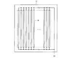
- the display liquid crystal panel 11 includes a plurality of analog switches 16 and a pixel array 17.
- the scanning signal line drive circuit 14 is formed integrally with the display liquid crystal panel 11.
- the liquid crystal display device 10 selectively performs planar display and stereoscopic display using a parallax barrier.
- the liquid crystal display device 10 performs polarity inversion driving and video signal line time-division driving.
- the display liquid crystal panel 11 is an active matrix TFT (Thin Film Transistor) liquid crystal panel.
- the display liquid crystal panel 11 includes n scanning signal lines G1 to Gn, 3m video signal lines SR1 to SRm, SG1 to SGm, SB1 to SBm, and (3m ⁇ n) pixel circuits 18. (Where m and n are integers of 2 or more).
- the n scanning signal lines are arranged in parallel to each other.
- the 3m video signal lines are arranged in parallel to each other so as to be orthogonal to the scanning signal lines.
- the scanning signal line extends in the vertical direction of the screen, and the video signal line extends in the horizontal direction of the screen.
- the pixel circuit 18 is disposed corresponding to each intersection of the scanning signal line and the video signal line, and is connected to the corresponding scanning signal line and the video signal line.
- the pixel circuit 18 is classified into an R pixel circuit for displaying red, a G pixel circuit for displaying green, and a B pixel circuit for displaying blue.
- Three types of pixel circuits 18 are connected to each video signal line for each type.
- n R pixel circuits are connected to the video signal line SR1.
- Three pixel circuits 18 arranged side by side in the extending direction of the scanning signal lines form one pixel.
- the display liquid crystal panel 11 has (m ⁇ n) pixels.
- the pixel circuit 18 is classified into a left-eye pixel circuit 21 for displaying a left-eye image and a right-eye pixel circuit 22 for displaying a right-eye image.
- the pixel array 17 includes a column in which the left-eye pixel circuits 21 are arranged in the vertical direction of the screen and a column in which the right-eye pixel circuits 22 are arranged in the vertical direction of the screen. It has a configuration that is arranged alternately in the direction.
- the left-eye pixel circuits 21 are arranged in the odd-numbered columns, and the right-eye pixel circuits 22 are arranged in the even-numbered columns.
- Three left-eye pixel circuits 21 arranged side by side in the extending direction of the scanning signal line form one left-eye pixel.
- the three right-eye pixel circuits 22 arranged side by side in the extending direction of the scanning signal line form one right-eye pixel.
- the video signal line driving circuit 15 has m output terminals S1 to Sm.
- the 3m video signal lines are divided into m groups of 3 according to the arrangement order, and are associated with the output terminals of the video signal line driving circuit 15 for each group.
- the display liquid crystal panel 11 is provided with 3m analog switches 16. One end of the analog switch 16 is connected to one of the video signal lines, and the other end is connected to the output terminal of the video signal line driving circuit 15 corresponding to the group to which the video signal line belongs.
- the display control circuit 13 is supplied with control signals such as a vertical synchronization signal VSYNC and a horizontal synchronization signal HSYNC and a video signal VS from the outside of the liquid crystal display device 10.
- the display control circuit 13 is supplied with a mode selection signal MD for switching between planar display and stereoscopic display. Based on these signals, the display control circuit 13 outputs a control signal C1 to the scanning signal line drive circuit 14, outputs a control signal C2 and a video signal VS to the video signal line drive circuit 15, and an analog switch. 16, switch control signals CR, CG, CB are output.
- the switch control signal CR is supplied to the analog switch 16 connected to the video signal lines SR1 to SRm, the switch control signal CG is supplied to the analog switch 16 connected to the video signal lines SG1 to SGm, and the switch control signal CB is the video.
- the signal is supplied to the analog switch 16 connected to the signal lines SB1 to SBm.
- the scanning signal line driving circuit 14 drives n scanning signal lines based on the control signal C1. More specifically, the scanning signal line driving circuit 14 selects one scanning signal line from the n scanning signal lines according to the arrangement order based on the control signal C1, and selects a selected voltage (for example, a high level voltage) is applied. As a result, the 3m pixel circuits 18 connected to the selected scanning signal line are selected at once.
- a selected voltage For example, a high level voltage
- the video signal line drive circuit 15 drives 3m video signal lines based on the control signal C2 and the video signal VS. More specifically, the video signal line driving circuit 15 divides one horizontal period into three periods (hereinafter referred to as first to third periods), and the video signal VS is output from the m output terminals S1 to Sm in each period. M signal voltages corresponding to are output.
- the analog switch 16 is turned on when the applied switch control signal is at a high level, and is turned off when the switch control signal is at a low level. For example, when the switch control signal CR is at a high level, the m analog switches 16 connected to the video signal lines SR1 to SRm are turned on, and the m signal voltages output from the video signal line driving circuit 15 are video. Applied to the signal lines SR1 to SRm. In this way, the analog switch 16 functions as a video signal line selection circuit that selects one video signal line from each group and applies the voltage output from the video signal line drive circuit 15 to the selected video signal line.
- the switch control signals CR, CG, CB are at a high level in any one of the first to third periods within one horizontal period in the order described later. As a result, a signal voltage is applied to the 3m video signal lines once in one horizontal period, and the signal voltage applied to the video signal lines is 3m pixel circuits selected using the scanning signal lines. 18 is written. By performing the above operation n times in one vertical period (one frame period), an image corresponding to the video signal VS is displayed on the display liquid crystal panel 11.
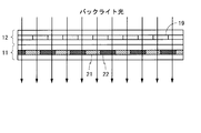
- the parallax barrier liquid crystal panel 12 is a TN (Twisted Nematic) type liquid crystal panel.
- FIG. 2 is a diagram illustrating a configuration of the parallax barrier liquid crystal panel 12.
- the parallax barrier liquid crystal panel 12 is provided with a plurality of shutter regions 19 that are long in the vertical direction of the screen.
- the shutter area 19 is in a transmissive state or a non-transmissive state according to the control signal CX output from the display control circuit 13.
- the shutter region 19 is in a transmissive state when the control signal CX is at a low level and is in a non-transmissive state when the control signal CX is at a high level.
- the parallax barrier liquid crystal panel 12 is provided on the back side of the display liquid crystal panel 11.
- the backlight is provided on the back side of the parallax barrier liquid crystal panel 12.
- the liquid crystal display device 10 selectively performs two-dimensional display for displaying an image two-dimensionally and three-dimensional display for displaying an image three-dimensionally according to a mode selection signal MD.
- a mode selection signal MD In order to perform stereoscopic display, it is necessary to display a left-eye image using the left-eye pixel circuit 21 and display a right-eye image using the right-eye pixel circuit 22.
- the left-eye image and the right-eye image are generated inside the display control circuit 13 or outside the liquid crystal display device 10.
- FIG. 3 is a diagram showing the pixel circuit 18 of the display liquid crystal panel 11 and the shutter region 19 of the parallax barrier liquid crystal panel 12 in an overlapping manner.
- the width of the shutter region 19 is substantially the same as the size of the video signal line of the pixel circuit 18 in the extending direction.
- the shutter area 19 is arranged so as to overlap the right half of the left-eye pixel circuit 21 and the left half of the right-eye pixel circuit 22.
- the display control circuit 13 outputs a low-level control signal CX to the parallax barrier liquid crystal panel 12.
- the shutter region 19 of the parallax barrier liquid crystal panel 12 is in a transmissive state. Since the backlight light passes through the transmissive shutter region 19, the same light reaches the human left eye and right eye. At this time, a human recognizes a planar image.
- the display control circuit 13 outputs a high-level control signal CX to the parallax barrier liquid crystal panel 12.
- the shutter region 19 of the parallax barrier liquid crystal panel 12 is in a non-transmissive state and functions as a parallax barrier.
- the backlight light is separated into two in the horizontal direction of the screen by the non-transparent shutter region 19.
- One light (denoted as L in FIG. 4B) passes through the left-eye pixel circuit 21 and reaches the human left eye.
- the other light (described as R in FIG. 4B) passes through the right eye pixel circuit 22 and reaches the human right eye.
- the liquid crystal display device 10 performs polarity inversion driving for switching the polarity of the liquid crystal applied voltage (hereinafter simply referred to as “voltage polarity”), and performs video signal line time-division driving for grouping three video signal lines. At this time, the liquid crystal display device 10 switches the signal voltage writing order (hereinafter simply referred to as “writing order”) to the pixel circuit 18 within one horizontal period.
- writing order the signal voltage writing order
- the order of R, G, and B is referred to as “normal order”
- the order of B, G, and R is referred to as “reverse order”.
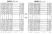
- FIG. 5A is a diagram showing a writing order and a voltage polarity at the time of planar display.
- the liquid crystal display device 10 switches the writing order and the voltage polarity for each scanning signal line in the flat display. More specifically, in the odd-numbered frame, the positive polarity voltage is written in the normal order to each pixel included in the odd-numbered column, and the negative polarity voltage is written in the reverse order to each pixel included in the even-numbered column. It is. In the even-numbered frame, the negative voltage is written in the reverse order to each pixel included in the odd-numbered column, and the positive voltage is written in the normal order to each pixel included in the even-numbered column.
- FIG. 5B is a diagram showing a writing order and voltage polarity in the stereoscopic display.
- the liquid crystal display device 10 switches the writing order and the voltage polarity for each of the two scanning signal lines during stereoscopic display.
- the pixels included in the pixel array 17 are for the first group of pixels for the left eye arranged in the first column, the fifth column, etc., and for the right eye arranged in the second column, the sixth column, etc.
- FIG. 6 shows a summary of the writing order and the voltage polarity during the stereoscopic display in the liquid crystal display device 10.
- FIG. 7A is a timing chart of odd-numbered frames in the planar display.
- the switch control signal CR becomes high level, and the video signal line driving circuit 15 has a positive signal voltage to be written to the R pixel circuit. Is output.
- the switch control signal CG becomes high level, and the video signal line driving circuit 15 outputs a positive signal voltage to be written to the G pixel circuit.
- the switch control signal CB becomes high level, and a positive signal voltage to be written to the B pixel circuit is output from the video signal line driving circuit 15.
- this change mode is referred to as a “first mode”.
- the switch control signal CB is at a high level, and a negative signal voltage to be written to the B pixel circuit is output from the video signal line driving circuit 15.
- the switch control signal CG becomes high level, and a negative signal voltage to be written to the G pixel circuit is output from the video signal line driving circuit 15.
- the switch control signal CR becomes high level, and a negative signal voltage to be written to the R pixel circuit is output from the video signal line driving circuit 15.
- this change mode is referred to as a “second mode”.
- the third and subsequent horizontal periods are the same as the first and second horizontal periods.
- FIG. 7B is a timing chart of even-numbered frames in the planar display.
- the switch control signals CR, CG, CB and the output of the video signal line drive circuit 15 change in the second manner in the first horizontal period of the even-numbered frame, and the second horizontal of the even-numbered frame. The period changes in the first manner.
- the third and subsequent horizontal periods are the same as the first and second horizontal periods.
- FIG. 8A is a timing chart of odd-numbered frames in the stereoscopic display.
- the switch control signals CR, CG, and CB and the output of the video signal line driving circuit 15 change in the first mode in the first and second horizontal periods of the odd-numbered frames, and the odd-numbered frames.
- the third and fourth horizontal periods change in the second manner.
- the fifth and subsequent horizontal periods are the same as the first to fourth horizontal periods.
- FIG. 8B is a timing chart of the even-numbered frame in the stereoscopic display.
- the switch control signals CR, CG, CB and the output of the video signal line driving circuit 15 change in the second mode in the first and second horizontal periods of the even-numbered frame,
- the third and fourth horizontal periods change in the first manner.
- the fifth and subsequent horizontal periods are the same as the first to fourth horizontal periods.
- the liquid crystal display device 10 since a parasitic capacitance exists between a video signal line and a pixel circuit, the potential held in the pixel circuit may fluctuate when a signal voltage is applied to the video signal line.
- the amount of potential variation depends on the order of writing. For this reason, when the writing order is fixed in a liquid crystal display device that performs video signal line time-division driving, periodic noise is generated in the potential held in the pixel circuit according to the writing order, and striped display unevenness occurs. There are things to do.
- the display unevenness generated in the color liquid crystal display device is recognized as a color shift (color shift) by humans.
- this method is not suitable for stereoscopic display.
- the writing order of the left-eye pixel is merely switched for each frame.
- the liquid crystal display device 10 switches the writing order for every two scanning signal lines during stereoscopic display (see FIG. 5B). Therefore, the writing order for the left-eye pixels can be switched for each line, and the writing order for the right-eye pixels can be switched for each line.
- the liquid crystal display device 10 according to the present embodiment switches the voltage polarity for every two scanning signal lines during stereoscopic display. Therefore, the voltage polarity for the left-eye pixel can be switched for each line, and the voltage polarity for the right-eye pixel can be switched for each line. Therefore, color shift and flicker can be prevented for both the left-eye image and the right-eye image.
- a method of switching the voltage polarity for each scanning signal line while switching the writing order for each of the two scanning signal lines is also conceivable.
- frame inversion driving is merely performed for the left-eye pixel and the right-eye pixel.
- signal voltage is written in a combination of (forward order, positive polarity) or (reverse order, negative polarity)
- the signal voltage is written in a combination of (reverse order, positive polarity) or (forward order, negative polarity).
- the signal voltage is a combination of (normal order, positive polarity) or (reverse order, negative polarity) for all pixels including the left-eye pixel and the right-eye pixel. Is written. In this manner, display uniformity can be prevented by aligning the combination of the writing order and the voltage polarity for every pixel.
- liquid crystal display device 10 switches the writing order and the voltage polarity for each scanning signal line during flat display. Therefore, the image quality can be improved in both stereoscopic display and planar display.
- the liquid crystal display device according to the second embodiment of the present invention has the same configuration as the liquid crystal display device according to the first embodiment (see FIG. 1).
- the liquid crystal display device according to the present embodiment is different from the liquid crystal display device according to the first embodiment only in the writing order and the voltage polarity at the time of stereoscopic display.
- differences from the first embodiment will be described.
- the liquid crystal display device according to the present embodiment switches the writing order and the voltage polarity for each horizontal period in flat display, and the writing order and voltage polarity in stereoscopic display. Is switched every two horizontal periods.
- FIG. 10 is a diagram showing the writing order and voltage polarity in the stereoscopic display in the liquid crystal display device according to the present embodiment.
- k is an integer of 1 or more.
- the voltage polarity is switched every two scanning signal lines.
- the voltage polarities of the four scanning signal lines arranged side by side are (positive, positive, negative, negative), (negative, negative, positive, positive), (positive, negative, negative, positive) for each frame. And (Negative, Positive, Positive, Negative). For this reason, for all video signal lines, the probability that the signal voltage having the same polarity will be written next is the same as the probability that the signal voltage having the different polarity will be written next. Thereby, the brightness
- the mode selection signal MD for switching between the flat display and the stereoscopic display is given to the liquid crystal display device from the outside, but the data for switching between the flat display and the stereoscopic display is used as an existing signal (for example, it may be superimposed on the blanking period portion of the video signal VS.
- the writing order may be switched every multiples of 2 scanning signal lines in the case of stereoscopic display.
- the image quality for the left-eye image and the right-eye image is improved by driving using the writing order and voltage polarity suitable for stereoscopic display, respectively.
- the image quality at the time of can be increased.
- the stereoscopic display device of the present invention has an effect of performing high-quality display by driving suitable for stereoscopic display, it can be used for various electronic devices having a stereoscopic display function such as a stereoscopic display television.
- SYMBOLS 10 Liquid crystal display device 11 ... Display liquid crystal panel 12 ... Liquid crystal panel for parallax barrier 13 ... Display control circuit 14 ... Scanning signal line drive circuit 15 ... Video signal line drive circuit 16 ... Analog switch 17 ... Pixel array 18 ... Pixel circuit 19 ... shutter region 21 ... pixel circuit for left eye 22 ... pixel circuit for right eye
Abstract
Description
画面の垂直方向に伸延する複数の走査信号線と、
画面の水平方向に伸延し、配置順に従い所定本数ずつグループ化される複数の映像信号線と、
前記走査信号線と前記映像信号線の交点に対応して配置された複数の画素回路を含む画素アレイと、
前記走査信号線を選択する走査信号線駆動回路と、
前記映像信号線の各グループに対して、グループ内の映像信号線に印加すべき電圧を1水平期間内に時分割で出力する映像信号線駆動回路と、
各グループから1本の映像信号線を選択し、選択した映像信号線に前記映像信号線駆動回路から出力された電圧を与える映像信号線選択回路とを備え、
前記画素アレイは、画面の垂直方向に左目用画素回路を並べて配置した列と、画面の垂直方向に右目用画素回路を並べて配置した列とを、画面の水平方向に並べた構成を有し、
1水平期間内での前記画素回路に対する書き込み順序が、2の倍数本の走査信号線ごとに切り替わることを特徴とする。
前記画素アレイは、前記左目用画素回路の列と前記右目用画素回路の列とを画面の水平方向に交互に並べた構成を有し、
前記書き込み順序が2本の走査信号線ごとに切り替わることを特徴とする。
画像を平面的に表示するときには、前記書き込み順序が1本の走査信号線ごとに切り替わることを特徴とする。
前記画素回路に書き込まれる電圧の極性が、2本の走査信号線ごとに切り替わることを特徴とする。
前記電圧の極性が、並べて配置された4本の走査信号線について、フレームごとに4とおりに切り替わることを特徴とする。
画像を平面的に表示するときには、前記電圧の極性が1本の走査信号線ごとに切り替わることを特徴とする。
前記走査信号線を選択するステップと、
前記映像信号線の各グループに対して、グループ内の映像信号線に印加すべき電圧を1水平期間内に時分割で出力するステップと、
各グループから1本の映像信号線を選択し、選択した映像信号線に時分割で出力された電圧を与えるステップとを備え、
前記画素アレイは、画面の垂直方向に左目用画素回路を並べて配置した列と、画面の垂直方向に右目用画素回路を並べて配置した列とを、画面の水平方向に並べた構成を有し、
1水平期間内での前記画素回路に対する書き込み順序を2の倍数本の走査信号線ごとに切り替えることを特徴とする。
図1は、本発明の第1の実施形態に係る液晶表示装置の構成を示すブロック図である。図1に示す液晶表示装置10は、表示用液晶パネル11、視差バリア用液晶パネル12、表示制御回路13、走査信号線駆動回路14、映像信号線駆動回路15、および、バックライト(図示せず)を備えている。表示用液晶パネル11は、複数のアナログスイッチ16と画素アレイ17を含んでいる。走査信号線駆動回路14は、表示用液晶パネル11と一体に形成されている。液晶表示装置10は、平面表示と視差バリアを用いた立体表示とを選択的に行う。また、液晶表示装置10は、極性反転駆動と映像信号線時分割駆動を行う。
本発明の第2の実施形態に係る液晶表示装置は、第1の実施形態に係る液晶表示装置と同じ構成を有する(図1を参照)。本実施形態に係る液晶表示装置は、第1の実施形態に係る液晶表示装置と、立体表示のときの書き込み順序と電圧極性のみが相異する。以下、第1の実施形態との相違点を説明する。
11…表示用液晶パネル
12…視差バリア用液晶パネル
13…表示制御回路
14…走査信号線駆動回路
15…映像信号線駆動回路
16…アナログスイッチ
17…画素アレイ
18…画素回路
19…シャッター領域
21…左目用画素回路
22…右目用画素回路
Claims (7)
- 画像を立体的に表示する機能を有する立体表示装置であって、
画面の垂直方向に伸延する複数の走査信号線と、
画面の水平方向に伸延し、配置順に従い所定本数ずつグループ化される複数の映像信号線と、
前記走査信号線と前記映像信号線の交点に対応して配置された複数の画素回路を含む画素アレイと、
前記走査信号線を選択する走査信号線駆動回路と、
前記映像信号線の各グループに対して、グループ内の映像信号線に印加すべき電圧を1水平期間内に時分割で出力する映像信号線駆動回路と、
各グループから1本の映像信号線を選択し、選択した映像信号線に前記映像信号線駆動回路から出力された電圧を与える映像信号線選択回路とを備え、
前記画素アレイは、画面の垂直方向に左目用画素回路を並べて配置した列と、画面の垂直方向に右目用画素回路を並べて配置した列とを、画面の水平方向に並べた構成を有し、
1水平期間内での前記画素回路に対する書き込み順序が、2の倍数本の走査信号線ごとに切り替わることを特徴とする、立体表示装置。 - 前記画素アレイは、前記左目用画素回路の列と前記右目用画素回路の列とを画面の水平方向に交互に並べた構成を有し、
前記書き込み順序が2本の走査信号線ごとに切り替わることを特徴とする、請求項1に記載の立体表示装置。 - 画像を平面的に表示するときには、前記書き込み順序が1本の走査信号線ごとに切り替わることを特徴とする、請求項2に記載の立体表示装置。
- 前記画素回路に書き込まれる電圧の極性が、2本の走査信号線ごとに切り替わることを特徴とする、請求項2に記載の立体表示装置。
- 前記電圧の極性が、並べて配置された4本の走査信号線について、フレームごとに4とおりに切り替わることを特徴とする、請求項4に記載の立体表示装置。
- 画像を平面的に表示するときには、前記電圧の極性が1本の走査信号線ごとに切り替わることを特徴とする、請求項4に記載の立体表示装置。
- 画面の垂直方向に伸延する複数の走査信号線と、画面の水平方向に伸延し、配置順に従い所定本数ずつグループ化される複数の映像信号線と、前記走査信号線と前記映像信号線の交点に対応して配置された複数の画素回路を含む画素アレイとを有する立体表示装置の駆動方法であって、
前記走査信号線を選択するステップと、
前記映像信号線の各グループに対して、グループ内の映像信号線に印加すべき電圧を1水平期間内に時分割で出力するステップと、
各グループから1本の映像信号線を選択し、選択した映像信号線に時分割で出力された電圧を与えるステップとを備え、
前記画素アレイは、画面の垂直方向に左目用画素回路を並べて配置した列と、画面の垂直方向に右目用画素回路を並べて配置した列とを、画面の水平方向に並べた構成を有し、
1水平期間内での前記画素回路に対する書き込み順序を2の倍数本の走査信号線ごとに切り替えることを特徴とする、立体表示装置の駆動方法。
Priority Applications (6)
| Application Number | Priority Date | Filing Date | Title |
|---|---|---|---|
| JP2011514368A JP5175977B2 (ja) | 2009-05-22 | 2010-04-16 | 立体表示装置 |
| CN201080010001.4A CN102341744B (zh) | 2009-05-22 | 2010-04-16 | 立体显示装置 |
| RU2011152389/28A RU2487379C1 (ru) | 2009-05-22 | 2010-04-16 | Устройство стереоскопического отображения |
| US13/254,028 US9083965B2 (en) | 2009-05-22 | 2010-04-16 | Stereoscopic display device |
| EP10777644.5A EP2434331B1 (en) | 2009-05-22 | 2010-04-16 | Stereoscopic display device |
| BRPI1010682A BRPI1010682A2 (pt) | 2009-05-22 | 2010-04-16 | dispositivo de exibição estereoscópica e método para acionar o mesmo |
Applications Claiming Priority (2)
| Application Number | Priority Date | Filing Date | Title |
|---|---|---|---|
| JP2009-124753 | 2009-05-22 | ||
| JP2009124753 | 2009-05-22 |
Publications (1)
| Publication Number | Publication Date |
|---|---|
| WO2010134409A1 true WO2010134409A1 (ja) | 2010-11-25 |
Family
ID=43126095
Family Applications (1)
| Application Number | Title | Priority Date | Filing Date |
|---|---|---|---|
| PCT/JP2010/056845 WO2010134409A1 (ja) | 2009-05-22 | 2010-04-16 | 立体表示装置 |
Country Status (7)
| Country | Link |
|---|---|
| US (1) | US9083965B2 (ja) |
| EP (1) | EP2434331B1 (ja) |
| JP (1) | JP5175977B2 (ja) |
| CN (1) | CN102341744B (ja) |
| BR (1) | BRPI1010682A2 (ja) |
| RU (1) | RU2487379C1 (ja) |
| WO (1) | WO2010134409A1 (ja) |
Cited By (2)
| Publication number | Priority date | Publication date | Assignee | Title |
|---|---|---|---|---|
| CN102752617A (zh) * | 2012-07-09 | 2012-10-24 | 京东方科技集团股份有限公司 | 一种3d显示方法及显示装置 |
| JP2013044992A (ja) * | 2011-08-25 | 2013-03-04 | Seiko Epson Corp | 電気光学装置および電子機器 |
Families Citing this family (14)
| Publication number | Priority date | Publication date | Assignee | Title |
|---|---|---|---|---|
| WO2011126090A1 (ja) * | 2010-04-08 | 2011-10-13 | シャープ株式会社 | 液晶表示装置および立体表示システム |
| KR101818567B1 (ko) * | 2011-05-18 | 2018-02-22 | 삼성디스플레이 주식회사 | 표시 패널의 구동 방법 및 이를 수행하는 표시 장치 |
| JP2013064920A (ja) * | 2011-09-20 | 2013-04-11 | Seiko Epson Corp | 電気光学装置および電子機器 |
| CN102982741A (zh) * | 2012-12-10 | 2013-03-20 | 京东方科技集团股份有限公司 | 阵列基板、3d显示装置及其驱动方法 |
| KR102019764B1 (ko) * | 2012-12-21 | 2019-09-09 | 엘지디스플레이 주식회사 | 액정표시장치 및 그 구동방법 |
| CN104280968B (zh) * | 2014-10-31 | 2017-10-17 | 深圳市华星光电技术有限公司 | 液晶显示面板及其3d显示时的像素插黑方法 |
| CN104410854B (zh) * | 2014-12-16 | 2017-07-18 | 上海天马微电子有限公司 | 一种3d面板及其驱动方法及电子设备 |
| CN104849929B (zh) | 2015-05-06 | 2018-09-04 | 深圳市华星光电技术有限公司 | 液晶显示面板及液晶显示装置 |
| WO2017208954A1 (ja) * | 2016-06-01 | 2017-12-07 | シャープ株式会社 | 映像信号線駆動回路およびそれを備える表示装置、ならびに映像信号線の駆動方法 |
| CN106959483A (zh) * | 2017-06-01 | 2017-07-18 | 宁波视睿迪光电有限公司 | 一种光栅膜及立体显示装置 |
| JP7021407B2 (ja) * | 2017-07-11 | 2022-02-17 | トライベイル テクノロジーズ, エルエルシー | 表示装置、及び、その駆動方法 |
| JP2019184856A (ja) * | 2018-04-12 | 2019-10-24 | シャープ株式会社 | 表示装置およびその駆動方法 |
| US20220224879A1 (en) * | 2019-05-30 | 2022-07-14 | Kyocera Corporation | Three-dimensional display device, head-up display system, and movable object |
| CN114170983B (zh) * | 2021-11-30 | 2023-04-07 | 京东方科技集团股份有限公司 | 显示装置、显示驱动方法及电子设备 |
Citations (7)
| Publication number | Priority date | Publication date | Assignee | Title |
|---|---|---|---|---|
| JPH0775135A (ja) | 1993-09-01 | 1995-03-17 | Sharp Corp | 3次元ディスプレイ装置 |
| JPH07175448A (ja) * | 1993-12-17 | 1995-07-14 | Canon Inc | 液晶表示装置 |
| JP2003058119A (ja) | 2001-08-09 | 2003-02-28 | Sharp Corp | アクティブマトリクス型表示装置及びその駆動方法、並びにそれに備えられる駆動制御回路 |
| JP2004037498A (ja) * | 2002-06-28 | 2004-02-05 | Seiko Epson Corp | 電気光学装置の駆動回路、電気光学装置、電子機器及び電気光学装置の駆動方法 |
| JP2005258013A (ja) | 2004-03-11 | 2005-09-22 | Sharp Corp | 表示パネルおよび表示装置 |
| JP2008089649A (ja) * | 2006-09-29 | 2008-04-17 | Nec Electronics Corp | 表示装置の駆動方法及び表示装置 |
| JP2008268421A (ja) * | 2007-04-18 | 2008-11-06 | Mitsubishi Electric Corp | 表示装置 |
Family Cites Families (19)
| Publication number | Priority date | Publication date | Assignee | Title |
|---|---|---|---|---|
| US5493427A (en) | 1993-05-25 | 1996-02-20 | Sharp Kabushiki Kaisha | Three-dimensional display unit with a variable lens |
| KR100302132B1 (ko) * | 1998-10-21 | 2001-12-01 | 구본준, 론 위라하디락사 | 싸이클 인버젼 방식 액정 패널 구동 방법 및 그 장치 |
| JP3956748B2 (ja) * | 2001-06-26 | 2007-08-08 | セイコーエプソン株式会社 | 表示装置、その駆動回路、その駆動方法および電子機器 |
| JP2003215497A (ja) * | 2002-01-24 | 2003-07-30 | Pioneer Electronic Corp | 空間像型表示装置 |
| JP2004309868A (ja) * | 2003-04-08 | 2004-11-04 | Sony Corp | 撮像装置及び立体映像生成装置 |
| JP2005345770A (ja) * | 2004-06-03 | 2005-12-15 | Nec Electronics Corp | 液晶パネル駆動方法,及び液晶表示装置 |
| JP4572095B2 (ja) * | 2004-07-15 | 2010-10-27 | Nec液晶テクノロジー株式会社 | 液晶表示装置、携帯機器及び液晶表示装置の駆動方法 |
| KR100932977B1 (ko) * | 2005-07-05 | 2009-12-21 | 삼성모바일디스플레이주식회사 | 입체 영상 표시 장치 |
| JP4783154B2 (ja) * | 2006-01-11 | 2011-09-28 | 東芝モバイルディスプレイ株式会社 | 平面表示装置及びその駆動方法 |
| JP2007310234A (ja) * | 2006-05-19 | 2007-11-29 | Nec Electronics Corp | データ線駆動回路、表示装置、及びデータ線駆動方法 |
| JP4714115B2 (ja) * | 2006-09-07 | 2011-06-29 | 株式会社東芝 | 立体映像表示装置および立体映像表示方法 |
| JP4706638B2 (ja) * | 2006-09-29 | 2011-06-22 | セイコーエプソン株式会社 | 表示装置、画像処理方法並びに電子機器 |
| CN101231402B (zh) * | 2007-01-26 | 2012-09-26 | 群康科技(深圳)有限公司 | 液晶显示面板 |
| KR101439842B1 (ko) * | 2007-06-25 | 2014-09-12 | 삼성전자주식회사 | 백라이트 유닛 및 이를 채용한 2d/3d 겸용영상표시장치 |
| US8446355B2 (en) * | 2007-10-15 | 2013-05-21 | Nlt Technologies, Ltd. | Display device, terminal device, display panel, and display device driving method |
| JP5665255B2 (ja) * | 2007-10-15 | 2015-02-04 | Nltテクノロジー株式会社 | 表示装置とその駆動方法、端末装置及び表示パネル |
| US20090179879A1 (en) * | 2008-01-10 | 2009-07-16 | Seiko Epson Corporation | Display device, method of driving display device, and electronic apparatus |
| KR100918065B1 (ko) * | 2008-03-31 | 2009-09-18 | 삼성모바일디스플레이주식회사 | 표시 장치 및 그의 구동 방법 |
| US20090322666A1 (en) * | 2008-06-27 | 2009-12-31 | Guo-Ying Hsu | Driving Scheme for Multiple-fold Gate LCD |
-
2010
- 2010-04-16 JP JP2011514368A patent/JP5175977B2/ja active Active
- 2010-04-16 CN CN201080010001.4A patent/CN102341744B/zh not_active Expired - Fee Related
- 2010-04-16 US US13/254,028 patent/US9083965B2/en not_active Expired - Fee Related
- 2010-04-16 EP EP10777644.5A patent/EP2434331B1/en not_active Not-in-force
- 2010-04-16 WO PCT/JP2010/056845 patent/WO2010134409A1/ja active Application Filing
- 2010-04-16 BR BRPI1010682A patent/BRPI1010682A2/pt not_active IP Right Cessation
- 2010-04-16 RU RU2011152389/28A patent/RU2487379C1/ru not_active IP Right Cessation
Patent Citations (7)
| Publication number | Priority date | Publication date | Assignee | Title |
|---|---|---|---|---|
| JPH0775135A (ja) | 1993-09-01 | 1995-03-17 | Sharp Corp | 3次元ディスプレイ装置 |
| JPH07175448A (ja) * | 1993-12-17 | 1995-07-14 | Canon Inc | 液晶表示装置 |
| JP2003058119A (ja) | 2001-08-09 | 2003-02-28 | Sharp Corp | アクティブマトリクス型表示装置及びその駆動方法、並びにそれに備えられる駆動制御回路 |
| JP2004037498A (ja) * | 2002-06-28 | 2004-02-05 | Seiko Epson Corp | 電気光学装置の駆動回路、電気光学装置、電子機器及び電気光学装置の駆動方法 |
| JP2005258013A (ja) | 2004-03-11 | 2005-09-22 | Sharp Corp | 表示パネルおよび表示装置 |
| JP2008089649A (ja) * | 2006-09-29 | 2008-04-17 | Nec Electronics Corp | 表示装置の駆動方法及び表示装置 |
| JP2008268421A (ja) * | 2007-04-18 | 2008-11-06 | Mitsubishi Electric Corp | 表示装置 |
Non-Patent Citations (1)
| Title |
|---|
| See also references of EP2434331A4 |
Cited By (3)
| Publication number | Priority date | Publication date | Assignee | Title |
|---|---|---|---|---|
| JP2013044992A (ja) * | 2011-08-25 | 2013-03-04 | Seiko Epson Corp | 電気光学装置および電子機器 |
| US9131212B2 (en) | 2011-08-25 | 2015-09-08 | Seiko Epson Corporation | Electro-optic apparatus and electronic apparatus |
| CN102752617A (zh) * | 2012-07-09 | 2012-10-24 | 京东方科技集团股份有限公司 | 一种3d显示方法及显示装置 |
Also Published As
| Publication number | Publication date |
|---|---|
| CN102341744B (zh) | 2014-10-15 |
| CN102341744A (zh) | 2012-02-01 |
| EP2434331A4 (en) | 2013-04-10 |
| BRPI1010682A2 (pt) | 2016-03-15 |
| EP2434331B1 (en) | 2015-03-04 |
| RU2011152389A (ru) | 2013-06-27 |
| US20110316989A1 (en) | 2011-12-29 |
| RU2487379C1 (ru) | 2013-07-10 |
| JP5175977B2 (ja) | 2013-04-03 |
| JPWO2010134409A1 (ja) | 2012-11-08 |
| US9083965B2 (en) | 2015-07-14 |
| EP2434331A1 (en) | 2012-03-28 |
Similar Documents
| Publication | Publication Date | Title |
|---|---|---|
| JP5175977B2 (ja) | 立体表示装置 | |
| JP4572095B2 (ja) | 液晶表示装置、携帯機器及び液晶表示装置の駆動方法 | |
| US9330617B2 (en) | Method of driving a display panel and display apparatus for performing the same | |
| RU2571403C2 (ru) | Автостереоскопическое устройство отображения | |
| KR101268057B1 (ko) | 입체영상표시장치 및 방법 | |
| JP2011076034A (ja) | 画像表示装置およびその駆動方法 | |
| TWI514843B (zh) | 光電裝置及電子機器 | |
| US9900590B2 (en) | Display panel and method of driving the same, and display device | |
| CN102340683A (zh) | 图像显示器及其驱动方法 | |
| US8179356B2 (en) | Method for driving liquid crystal display with inserting gray image | |
| CN102967940A (zh) | 显示装置和电子设备 | |
| US9123305B2 (en) | Electro-optical apparatus and electronics device | |
| US9177495B2 (en) | Electro-optical device and electronic apparatus | |
| JPH09149434A (ja) | カラー立体画像表示装置 | |
| US9019264B2 (en) | Electro-optical device and electronic apparatus | |
| US10891909B2 (en) | Display device and method for driving same | |
| KR101904472B1 (ko) | 입체 영상 표시장치 | |
| KR20110113967A (ko) | 입체 영상 표시장치와 그 구동방법 | |
| US20150130854A1 (en) | Liquid-crystal display device and method for driving same | |
| KR101992161B1 (ko) | 입체 영상 표시장치와 그 극성 제어 방법 | |
| JP2012249013A (ja) | 表示装置および表示方法 |
Legal Events
| Date | Code | Title | Description |
|---|---|---|---|
| WWE | Wipo information: entry into national phase |
Ref document number: 201080010001.4 Country of ref document: CN |
|
| 121 | Ep: the epo has been informed by wipo that ep was designated in this application |
Ref document number: 10777644 Country of ref document: EP Kind code of ref document: A1 |
|
| WWE | Wipo information: entry into national phase |
Ref document number: 2011514368 Country of ref document: JP |
|
| WWE | Wipo information: entry into national phase |
Ref document number: 5316/CHENP/2011 Country of ref document: IN |
|
| WWE | Wipo information: entry into national phase |
Ref document number: 2010777644 Country of ref document: EP |
|
| WWE | Wipo information: entry into national phase |
Ref document number: 13254028 Country of ref document: US |
|
| NENP | Non-entry into the national phase |
Ref country code: DE |
|
| ENP | Entry into the national phase |
Ref document number: 2011152389 Country of ref document: RU Kind code of ref document: A |
|
| REG | Reference to national code |
Ref country code: BR Ref legal event code: B01A Ref document number: PI1010682 Country of ref document: BR |
|
| ENP | Entry into the national phase |
Ref document number: PI1010682 Country of ref document: BR Kind code of ref document: A2 Effective date: 20111121 |