WO2010110169A1 - 載置台構造及び処理装置 - Google Patents
載置台構造及び処理装置 Download PDFInfo
- Publication number
- WO2010110169A1 WO2010110169A1 PCT/JP2010/054668 JP2010054668W WO2010110169A1 WO 2010110169 A1 WO2010110169 A1 WO 2010110169A1 JP 2010054668 W JP2010054668 W JP 2010054668W WO 2010110169 A1 WO2010110169 A1 WO 2010110169A1
- Authority
- WO
- WIPO (PCT)
- Prior art keywords
- heater
- power supply
- outermost peripheral
- mounting table
- outermost
- Prior art date
- Legal status (The legal status is an assumption and is not a legal conclusion. Google has not performed a legal analysis and makes no representation as to the accuracy of the status listed.)
- Ceased
Links
Images



Classifications
-
- C—CHEMISTRY; METALLURGY
- C23—COATING METALLIC MATERIAL; COATING MATERIAL WITH METALLIC MATERIAL; CHEMICAL SURFACE TREATMENT; DIFFUSION TREATMENT OF METALLIC MATERIAL; COATING BY VACUUM EVAPORATION, BY SPUTTERING, BY ION IMPLANTATION OR BY CHEMICAL VAPOUR DEPOSITION, IN GENERAL; INHIBITING CORROSION OF METALLIC MATERIAL OR INCRUSTATION IN GENERAL
- C23C—COATING METALLIC MATERIAL; COATING MATERIAL WITH METALLIC MATERIAL; SURFACE TREATMENT OF METALLIC MATERIAL BY DIFFUSION INTO THE SURFACE, BY CHEMICAL CONVERSION OR SUBSTITUTION; COATING BY VACUUM EVAPORATION, BY SPUTTERING, BY ION IMPLANTATION OR BY CHEMICAL VAPOUR DEPOSITION, IN GENERAL
- C23C16/00—Chemical coating by decomposition of gaseous compounds, without leaving reaction products of surface material in the coating, i.e. chemical vapour deposition [CVD] processes
- C23C16/44—Chemical coating by decomposition of gaseous compounds, without leaving reaction products of surface material in the coating, i.e. chemical vapour deposition [CVD] processes characterised by the method of coating
- C23C16/46—Chemical coating by decomposition of gaseous compounds, without leaving reaction products of surface material in the coating, i.e. chemical vapour deposition [CVD] processes characterised by the method of coating characterised by the method used for heating the substrate
-
- C—CHEMISTRY; METALLURGY
- C23—COATING METALLIC MATERIAL; COATING MATERIAL WITH METALLIC MATERIAL; CHEMICAL SURFACE TREATMENT; DIFFUSION TREATMENT OF METALLIC MATERIAL; COATING BY VACUUM EVAPORATION, BY SPUTTERING, BY ION IMPLANTATION OR BY CHEMICAL VAPOUR DEPOSITION, IN GENERAL; INHIBITING CORROSION OF METALLIC MATERIAL OR INCRUSTATION IN GENERAL
- C23C—COATING METALLIC MATERIAL; COATING MATERIAL WITH METALLIC MATERIAL; SURFACE TREATMENT OF METALLIC MATERIAL BY DIFFUSION INTO THE SURFACE, BY CHEMICAL CONVERSION OR SUBSTITUTION; COATING BY VACUUM EVAPORATION, BY SPUTTERING, BY ION IMPLANTATION OR BY CHEMICAL VAPOUR DEPOSITION, IN GENERAL
- C23C16/00—Chemical coating by decomposition of gaseous compounds, without leaving reaction products of surface material in the coating, i.e. chemical vapour deposition [CVD] processes
- C23C16/44—Chemical coating by decomposition of gaseous compounds, without leaving reaction products of surface material in the coating, i.e. chemical vapour deposition [CVD] processes characterised by the method of coating
- C23C16/458—Chemical coating by decomposition of gaseous compounds, without leaving reaction products of surface material in the coating, i.e. chemical vapour deposition [CVD] processes characterised by the method of coating characterised by the method used for supporting substrates in the reaction chamber
- C23C16/4582—Rigid and flat substrates, e.g. plates or discs
- C23C16/4583—Rigid and flat substrates, e.g. plates or discs the substrate being supported substantially horizontally
- C23C16/4586—Elements in the interior of the support, e.g. electrodes, heating or cooling devices
-
- H—ELECTRICITY
- H01—ELECTRIC ELEMENTS
- H01J—ELECTRIC DISCHARGE TUBES OR DISCHARGE LAMPS
- H01J37/00—Discharge tubes with provision for introducing objects or material to be exposed to the discharge, e.g. for the purpose of examination or processing thereof
- H01J37/32—Gas-filled discharge tubes
- H01J37/32009—Arrangements for generation of plasma specially adapted for examination or treatment of objects, e.g. plasma sources
- H01J37/32082—Radio frequency generated discharge
- H01J37/32091—Radio frequency generated discharge the radio frequency energy being capacitively coupled to the plasma
-
- H—ELECTRICITY
- H05—ELECTRIC TECHNIQUES NOT OTHERWISE PROVIDED FOR
- H05B—ELECTRIC HEATING; ELECTRIC LIGHT SOURCES NOT OTHERWISE PROVIDED FOR; CIRCUIT ARRANGEMENTS FOR ELECTRIC LIGHT SOURCES, IN GENERAL
- H05B3/00—Ohmic-resistance heating
- H05B3/20—Heating elements having extended surface area substantially in a two-dimensional [2D] plane, e.g. plate-heater
- H05B3/22—Heating elements having extended surface area substantially in a two-dimensional [2D] plane, e.g. plate-heater non-flexible
-
- H—ELECTRICITY
- H10—SEMICONDUCTOR DEVICES; ELECTRIC SOLID-STATE DEVICES NOT OTHERWISE PROVIDED FOR
- H10P—GENERIC PROCESSES OR APPARATUS FOR THE MANUFACTURE OR TREATMENT OF DEVICES COVERED BY CLASS H10
- H10P72/00—Handling or holding of wafers, substrates or devices during manufacture or treatment thereof
- H10P72/04—Apparatus for manufacture or treatment
- H10P72/0431—Apparatus for thermal treatment
- H10P72/0432—Apparatus for thermal treatment mainly by conduction
-
- H—ELECTRICITY
- H10—SEMICONDUCTOR DEVICES; ELECTRIC SOLID-STATE DEVICES NOT OTHERWISE PROVIDED FOR
- H10P—GENERIC PROCESSES OR APPARATUS FOR THE MANUFACTURE OR TREATMENT OF DEVICES COVERED BY CLASS H10
- H10P72/00—Handling or holding of wafers, substrates or devices during manufacture or treatment thereof
- H10P72/04—Apparatus for manufacture or treatment
- H10P72/0431—Apparatus for thermal treatment
- H10P72/0434—Apparatus for thermal treatment mainly by convection
-
- H—ELECTRICITY
- H10—SEMICONDUCTOR DEVICES; ELECTRIC SOLID-STATE DEVICES NOT OTHERWISE PROVIDED FOR
- H10P—GENERIC PROCESSES OR APPARATUS FOR THE MANUFACTURE OR TREATMENT OF DEVICES COVERED BY CLASS H10
- H10P72/00—Handling or holding of wafers, substrates or devices during manufacture or treatment thereof
- H10P72/06—Apparatus for monitoring, sorting, marking, testing or measuring
- H10P72/0602—Temperature monitoring
-
- H—ELECTRICITY
- H01—ELECTRIC ELEMENTS
- H01J—ELECTRIC DISCHARGE TUBES OR DISCHARGE LAMPS
- H01J2237/00—Discharge tubes exposing object to beam, e.g. for analysis treatment, etching, imaging
- H01J2237/20—Positioning, supporting, modifying or maintaining the physical state of objects being observed or treated
- H01J2237/2001—Maintaining constant desired temperature
-
- H—ELECTRICITY
- H05—ELECTRIC TECHNIQUES NOT OTHERWISE PROVIDED FOR
- H05B—ELECTRIC HEATING; ELECTRIC LIGHT SOURCES NOT OTHERWISE PROVIDED FOR; CIRCUIT ARRANGEMENTS FOR ELECTRIC LIGHT SOURCES, IN GENERAL
- H05B2203/00—Aspects relating to Ohmic resistive heating covered by group H05B3/00
- H05B2203/037—Heaters with zones of different power density
Definitions
- the present invention relates to a processing apparatus for performing a heat treatment such as a plasma process or a film forming process on an object to be processed such as a semiconductor wafer, and a mounting table structure used therefor.
- a semiconductor device such as an IC (integrated circuit)
- various processes such as a film formation process, an etching process, a heat treatment, and a modification process are performed on a target object such as a semiconductor wafer by using plasma.
- the target circuit device or the like is manufactured repeatedly without using plasma.
- a mounting table structure including a resistance heater is installed in a processing container that can be evacuated.
- a predetermined processing gas is flowed in a state where the semiconductor wafer is mounted on the upper surface of the mounting table structure, and various heat treatments are performed on the wafer under predetermined process conditions using plasma or without plasma (special characteristics). No. 63-278322, JP 07-077866, JP 06-260430, JP 2004-356624, JP 10-209255, etc.).
- the semiconductor wafer is exposed to a high temperature, and a corrosive gas such as a cleaning gas or an etching gas is used in the processing container.
- a corrosive gas such as a cleaning gas or an etching gas
- ceramics represented by AlN (aluminum nitride) tend to be used for the mounting table structure on which the semiconductor wafer is mounted.
- a heater or an electrostatic chuck electrode is provided in the mounting table structure, they are integrally embedded in the ceramic.
- FIG. 9 is a schematic diagram showing a conventional processing apparatus using plasma
- FIG. 10 is a plan view showing a resistance heater having a mounting table structure.
- FIG. 9 shows a plasma processing apparatus as an example of the processing apparatus, and a mounting table structure 4 for mounting the semiconductor wafer W on the upper surface is provided in the cylindrical processing container 2.
- a shower head 6 is provided as a gas introduction means on the ceiling of the processing container 2, and necessary gas is injected from the gas injection holes 6 ⁇ / b> A on the lower surface of the shower head 6.
- the shower head 6 is connected to a high frequency power source 8 for generating plasma, for example, 13.56 MHz, so that the shower head 6 functions as an upper electrode.
- the mounting table structure 4 includes a mounting table main body 16 on which the wafer W is mounted, and a support column 18 that stands up from the bottom of the container and supports the mounting table main body 16.
- the mounting table main body 16 is made of ceramic such as AlN having heat resistance and corrosion resistance, and an electrode 20 serving as a lower electrode and a chuck electrode of the electrostatic chuck is embedded therein.
- a heating means 22 composed of a resistance heater 24 is embedded under the electrode 20 to heat the wafer W.
- the resistance heater 24 that constitutes the heating means 22 includes a resistance heater 24A and a resistance heater 24B that are provided in the inner and outer peripheral zones divided concentrically. .
- the resistance heaters 24A and 24B in each zone are individually controlled to achieve in-plane temperature uniformity of the wafer W.
- Each portion of the side wall of the processing vessel 2 is appropriately provided with a gate valve 12, an observation window 14, an attachment port (not shown) for attaching various measuring instruments, and the like. Parts and thermal conditions are different. For example, the temperature of the attachment portion of the gate valve 12 tends to decrease because the gate valve 12 is repeatedly opened and closed for loading and unloading of the wafer W.
- the portion where the observation window 14 is provided may differ from the ambient temperature because quartz glass, which is a constituent material of the observation window 14, has a specific heat different from that of a metal such as an aluminum alloy, which is a constituent material of the container side wall. is there. Under such circumstances, the peripheral portion of the wafer W is likely to be locally adversely affected by heat from the mounting portion of the gate valve 12 and the mounting portion of the observation window 14 having different temperatures.
- the resistance heater 24B in the outer peripheral zone that controls the temperature of the peripheral portion of the wafer W can only perform overall temperature control. For this reason, when the peripheral part of the wafer is locally affected by heat, this cannot be effectively dealt with, and therefore the in-plane uniformity of the wafer temperature is reduced. was there.
- the present invention provides a mounting table structure and a processing apparatus capable of controlling the temperature distribution in the peripheral portion of the object to be processed with a simple configuration.
- the present invention provides a mounting table structure for mounting the object to be processed in order to perform a heat treatment on the object to be processed in a processing container, wherein the object to be processed is mounted on an upper surface and concentrically.
- a mounting table main body divided into a plurality of heating zones, and a plurality of resistance heaters provided in the mounting table main body, wherein each heating heater is provided corresponding to each of the heating zones.
- a plurality of power supply lines for supplying power to the plurality of resistance heaters, wherein the resistance heaters in different heating zones are connected to different power supply lines.
- a heater controller provided so that the power supplied to the resistance heater can be controlled independently for each heating zone, and the plurality of resistance heaters include the plurality of heating heaters.
- An outermost resistance heater that is a resistance heater located in the outermost heating zone of the outermost heating zone, the outermost resistance heating heater extending in a circumferential direction of the outermost heating zone,
- the power supply line includes a plurality of outermost power supply lines for supplying power to the outermost peripheral resistance heater, and the outermost power supply lines are respectively connected to a plurality of different positions in the circumferential direction of the outermost resistance heater.
- the outermost peripheral resistance heater is partitioned at the plurality of positions to partition a plurality of heater sections, and the heater control unit individually controls the electrical state of each outermost peripheral power supply line.
- a mounting table structure configured to be able to Preferably, the outermost peripheral resistance heater is an endless heater continuously extending over the entire circumference of the outermost heating zone.
- the heater control unit has a plurality of different power supply modes for the outermost peripheral resistance heater, and the power supply mode is a combination of electrical states of the outermost power feed lines,
- the heater control unit is configured to switch the plurality of power supply modes by time division control.
- the outermost peripheral resistance heater can be divided into an even number of heater sections.
- the heater control unit can be configured to have a power supply mode in which a current is supplied to all the heater sections of the outermost peripheral resistance heater.
- the heater control unit may be configured to have a power supply mode in which a current is supplied to two selected opposing heater sections.
- the heater control unit may be configured to have a power supply mode in which a current is supplied to two selected adjacent heater sections.
- the outermost peripheral resistance heater can be divided into an odd number of heater sections.
- the heater control unit may be configured to have a power supply mode in which a current is supplied to two selected adjacent heater sections.
- the heater control unit can be configured so that a selected power supply line among the outermost peripheral power supply lines can be in a floating state.
- the number of the outermost peripheral resistance heaters can be three or more.
- the mounting table main body can be made of ceramic material or quartz.
- the present invention provides a processing container for performing a heat treatment on an object to be processed, a processing container that can be evacuated, and the mounting table provided in the processing container for mounting the object to be processed.
- a processing apparatus having a structure and gas introduction means for introducing gas into the processing container.
- FIG. 1 It is a block diagram which shows the processing apparatus which has the mounting base structure which concerns on this invention. It is a schematic sectional drawing which shows the inside of a processing container. It is a top view which shows arrangement
- FIG. 1 is a block diagram showing a processing apparatus having a mounting table structure according to the present invention
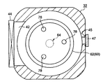
- FIG. 2 is a schematic sectional view showing the inside of a processing container
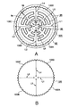
- FIG. 3 is a plan view showing the arrangement of resistance heaters of heating means.
- a parallel plate type plasma processing apparatus 30 includes a processing container 32 formed into a cylindrical shape by, for example, an aluminum alloy.
- an exhaust space 34 is provided by being further recessed downward and is defined by a bottomed cylindrical partition wall 36.
- the bottom of the partition wall 36 is the same as the bottom of the container. Has become a department.
- An exhaust port 38 is provided in the side wall of the partition wall 36, and an exhaust pipe 40 having a pressure adjusting valve, a vacuum pump, or the like (not shown) interposed in the middle is connected to the exhaust port 38.
- a vacuum can be drawn to a desired pressure.
- a loading / unloading port 42 for loading / unloading a semiconductor wafer W as an object to be processed is formed on the side wall of the processing container 32, and a gate valve 44 is provided at the loading / unloading port 42.
- the gate valve 44 is opened and closed when W is carried in and out.
- An observation window 47 made of, for example, quartz glass is airtightly provided on a side wall portion opposite to the gate valve 44 through a seal member 45 such as an O-ring so that the inside of the processing vessel 32 can be observed as necessary. It has become.
- Various members that can cause a thermal imbalance of a port or the like (not shown) for attaching various measuring devices are attached to the side wall of the processing vessel 32.
- the ceiling of the processing vessel 32 is opened, and a shower head 48 as a gas introduction unit is provided through the insulating member 46 in the opening.
- a sealing member 50 such as an O-ring is interposed between the shower head 48 and the insulating member 46 in order to maintain airtightness in the container.
- a gas introduction port 52 is provided in the upper part of the shower head 48, and a plurality of gas injection holes 54 are provided in the gas injection surface on the lower surface of the shower head 48, so that a necessary processing gas is directed toward the processing space S. It can be jetted.
- the shower head 48 has only one space, but a shower head of a type in which the internal space is divided into a plurality of parts and different gases are separately supplied to the processing space S without being mixed in the shower head 48 is used. May be.
- the shower head 48 has a function as an upper electrode for generating plasma.
- a high frequency power source 58 for generating plasma is connected to the shower head 48 via a matching circuit 56.
- the frequency of the high frequency power source 58 is, for example, 13.56 MHz, but is not limited to this frequency.
- a mounting table structure 60 according to the present invention is provided for mounting the semiconductor wafer W.
- the mounting table structure 60 has a disk-shaped mounting table main body 62 for mounting the wafer W directly on the mounting surface which is the upper surface thereof.
- the mounting table main body 62 is supported by a support column 64 provided upright from the bottom of the container.
- the lift pin mechanism 66 that pushes up and supports the wafer W from below when the wafer W is carried in and out.
- the lift pin mechanism 66 has, for example, three (only two are shown) lift pins 68 arranged at equal intervals along the circumferential direction of the mounting table main body 62.
- the lower end portion of each lifting pin 68 is supported by, for example, an arc-shaped pin base plate 70.
- the pin base plate 70 is connected to an elevating rod 72 that penetrates the bottom of the container, and the elevating rod 72 is attached to an actuator 74 that moves the elevating rod 72 up and down.
- An extendable bellows 76 that allows the vertical movement of the lifting rod 72 while maintaining airtightness inside the processing container 32 is provided at a portion through which the lifting rod 72 penetrates at the bottom of the processing container. *
- the mounting table main body 62 is provided with pin insertion holes 78 corresponding to the lifting pins 68.
- the lifting pins 68 inserted into the pin insertion holes 78 appear and disappear from the mounting surface of the mounting table main body 62 so that the wafer W can be moved up and down.
- the entire mounting table body 62 and the entire support column 64 are made of a material that does not cause metal contamination and has excellent heat resistance, such as a ceramic material or quartz.
- the support column 64 has a cylindrical shape, and the upper end of the support column 64 is, for example, heat diffusion bonded to the center of the lower surface (back surface) of the mounting table main body 62.
- the lower end portion of the support column 64 is connected to a peripheral portion of the opening 82 formed in the bottom portion of the processing container with a bolt (not shown) or the like via a seal member 80 such as an O-ring to maintain airtightness in the processing container 32.
- As the ceramic material aluminum nitride (AlN), aluminum oxide (Al 2 O 3 ), silicon carbide (SiC), or the like can be used.
- the mounting table main body 62 is embedded with a chuck electrode 84 of an electrostatic chuck and a resistance heater group 88 as a heating element as a heating means.
- the chuck electrode 84 is provided directly under the mounting surface and generates an electrostatic force for holding the wafer W by suction.
- a resistance heater group 88 for heating the wafer W is provided below the chuck electrode 84.
- the chuck electrode 84 also serves as a lower electrode for plasma generation.
- a DC power source (not shown) that generates a high voltage for wafer adsorption via a chuck power supply line (not shown) and a high-frequency power source (not shown) that applies a bias voltage for attracting plasma ions are applied to the chuck electrode 84. ) And are connected.
- the resistance heater group 88 is connected to a power supply line L (L1 to L6).
- the power supply line L is drawn out of the processing vessel 32 through the cylindrical support column 64.
- Each power supply line L is connected to a heater control unit 92 having a heater power supply and a computer, and controls the temperature of the wafer W by controlling the power supplied to the resistance heater group 88.
- a thermocouple (not shown) is provided below the mounting table main body 62, and the output is input to the heater control unit 92.
- An inert gas such as N 2 or Ar is supplied into the support column 64, thereby preventing corrosion of the power supply line L and the like.
- the mounting table main body 62 is divided into a plurality of concentric heating zones (hereinafter also referred to as “zones”). In the illustrated example, it is divided into two concentric (annular) zones, a circular inner peripheral zone 94 at the center of the mounting table main body 62 and a ring-shaped outer peripheral zone 96 surrounding the inner peripheral zone 94. In the illustrated example, since the outer peripheral zone 96 is located on the outermost periphery, it becomes the outermost peripheral zone.
- the resistance heater group 88 includes a resistance heater 98 provided in the inner peripheral zone 94 and a resistance heater 100 provided in the outer peripheral zone 96. Resistance heaters 98 and 100 provided in different zones are connected to different power supply lines L, respectively.
- 3A shows the arrangement of the resistance heaters 98 and 100 in the entire inner and outer peripheral zones 94 and 96, and FIG. 3B shows only the arrangement of the resistance heater 100 in the outer peripheral zone 96. Yes.
- Both ends of the resistance heater 98 in the inner peripheral zone 94 are connected to power supply lines L5 and L6, respectively.
- the resistance heater 98 extends from the one end connected to the power supply line L5 to the other end connected to the power supply line L6 continuously and without interruption, extending in a zigzag over the entire area of the inner peripheral zone 94. ing.
- the resistance heater 100 disposed in the outer peripheral zone 96 which is the outermost peripheral zone, that is, the outermost peripheral resistance heater is along the circumferential direction of the outer peripheral zone 96 (in the illustrated example, the circumferential direction while meandering the outer peripheral zone 96) Along the entire circumference), and as a whole, it is an endless ring (annular).
- the arrangement pattern of each resistance heater 98,100 is not specifically limited to each said pattern.
- the resistance heater 100 (hereinafter also referred to as “outermost resistance heater”) that is the outermost resistance heater is different from the power supply lines L5 and L6 for the inner peripheral zone 94 at a plurality of positions in the circumferential direction. Feed lines L1 to L4 are connected. That is, the outermost peripheral resistance heater 100 is divided into a plurality of heater sections with the connection points of the power supply lines L1 to L4 as boundaries.
- the outermost peripheral resistance heater 100 is connected to four power supply lines L1, L2, L3, and L4 at positions where the circumference is equally divided into four (even numbers), respectively. 100 is divided into four heater sections 100A, 100B, 100C, and 100D. Since the power supply lines L1 to L4 are connected to the outermost peripheral resistance heater 100, they are also referred to as “outermost peripheral power supply lines”.
- the outermost peripheral power supply lines L1 to L4 extend to the center of the mounting table main body 62 and are connected to the heater control unit 92 through the cylindrical support column 64 as described above. By controlling the electrical state of these outermost peripheral power supply lines L1 to L4, various combinations of electric power supplied to the heater sections 100A to 100D (currents flowing through the heater sections 100A to 100D) can be realized. it can.
- thermocouple (not shown) is provided on the back surface (lower surface) side of the mounting table main body 62, and a temperature measurement value by the thermocouple is input to the heater control unit 92, and the mounting is performed based on the measurement value. The entire temperature of the mounting body 62 is controlled.
- a thermocouple may be provided for each zone, or a thermocouple may be provided for each zone and the outermost peripheral zone may be provided for each of the heater sections 100A to 100D.
- the entire operation of the plasma processing apparatus 30 is controlled by an apparatus control unit 102 including, for example, a computer.
- Computer programs for performing this operation include flexible disks, CDs (Compact Discs), hard disks, It is stored in a storage medium 104 such as a flash memory or a DVD.
- a storage medium 104 such as a flash memory or a DVD.
- the start, stop and flow control of each gas, the supply and control of microwaves and high frequencies, the control of process temperature and process pressure, and the like are performed according to commands from the apparatus control unit 102.
- the heater control section 92 operates under the control of the apparatus control section 102.
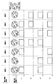
- FIG. 4 is a diagram showing the relationship between the state of the outermost power supply line and the power supply mode when the outermost peripheral zone is divided into four sections
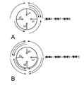
- FIG. 5 is the electric power when a specific heater section is controlled to a high temperature or a low temperature. It is a figure which shows an example of the change of a supply aspect.
- an unprocessed semiconductor wafer W is loaded into the processing container 32 through a gate valve 44 and a loading / unloading port 42 which are held by a transfer arm (not shown) and opened, and the wafer W is moved up and down. After being transferred to the pins 68, the elevating pins 68 are lowered to place the wafer W on the upper surface of the mounting table body 62 of the mounting table structure 60.
- film forming gas is supplied to the shower head 48 as various processing gases while controlling the flow rate, and this gas is injected from the gas injection hole 54 and introduced into the processing space S.
- a vacuum pump not shown
- the atmosphere in the processing vessel 32 and the exhaust space 34 is evacuated, and a pressure regulating valve (not shown) is provided.
- the atmosphere of the processing space S is maintained at a predetermined process pressure by adjusting the valve opening.
- the temperature of the wafer W is maintained at a predetermined process temperature.
- the resistance heater group 88 which is the heating means 86 of the mounting table main body 62 from the heater control unit 92 incorporating the heater power supply via the power supply line L (L1 to L6), the resistance heater group. 88 is heated, whereby the entire mounting table main body 62 is heated.
- the wafer W mounted on the mounting table main body 62 is heated to raise the temperature.
- the wafer temperature is measured by a thermocouple (not shown) provided on the mounting table main body 62, and the heater control unit 92 performs temperature control based on the measured value.
- the mode of temperature control will be described later.
- a high-frequency power source 58 is driven to apply a high-frequency voltage between the shower head 48 as the upper electrode and the mounting table body 62 as the lower electrode.
- a high-voltage DC voltage is applied to the chuck electrode 84 forming the electrostatic chuck, and the wafer W is attracted by electrostatic force.
- a predetermined plasma process is performed.
- plasma ions can be attracted by applying a high frequency from a high frequency power source (not shown) for bias to the chuck electrode 84 of the mounting table main body 62.
- the plasma processing is performed on the surface of the wafer W, for example, a thin film is formed.
- the heater control unit 92 transfers the resistance heating heaters 98 and 100 in the zones 94 and 96 to each other by feedback control. Individually controlled power is supplied.
- the heater control unit 92 includes a switching element such as a thyristor, and by driving the switching element, power is supplied to each of the resistance heaters 98 and 100 in a time-sharing manner. It has become. Electric power is supplied to the resistance heater 98 in the inner peripheral zone 94 through the feed lines L5 and L6 by feedback control, and the temperature control of the inner peripheral zone 94 is performed as a whole.
- the outermost peripheral resistance heater 100 which is a resistance heater in the outermost peripheral zone (outer peripheral zone) 96 is divided into four heater sections 100A to 100D in the circumferential direction, and the four outermost peripheral power supply lines L1 to By individually changing the electrical state (potential etc.) of L4, the power supply mode to the heater sections 100A to 100D can be changed.
- the gate valve 12 and the observation window 14 provided on the side wall of the processing container 2 are not thermally balanced. Under the influence of the members that generate, the temperature in the area around the wafer near these members will be locally higher or lower than other parts, reducing the in-plane uniformity of the wafer temperature. It was a cause.
- the outermost peripheral resistance heater 100 in the outermost peripheral zone 96 is divided into a plurality of, for example, four heater sections 100A to 100D, and the electric power of each heater section is divided.
- Supply control that is, temperature control can be performed individually. For this reason, even if there is a member that causes thermal imbalance such as the gate valve 44 and the observation window 47 as described above, this thermal influence can be compensated and suppressed. The uniformity of the in-plane temperature can be improved.
- FIG. 4 shows the potentials (applied voltages) of the outermost peripheral power supply lines L1 to L4 in each aspect, and means that a voltage (for example, 200 volts) is applied to the power supply line when a pulse is set.
- a voltage for example, 200 volts
- the applied voltage of the power supply line is zero (0) volts, that is, the power supply line is grounded.
- modes 1 to 7 are shown as examples of the power supply mode, and the current flowing direction at this time is indicated by an arrow in each heater section of the outermost peripheral zone 96.
- the temperature control of the outermost peripheral zone 96 is performed by appropriately selecting these modes 1 to 7 and switching them in a time division manner.
- Mode 1 by applying a voltage to the outermost peripheral power supply lines L1 and L3 and setting the outermost peripheral power supply lines L2 and L4 to 0 volts, it is possible to pass a current through all the heater sections 100A to 100D. In this case, the outermost peripheral zone 96 is heated uniformly. Note that even if a voltage is applied to the outermost peripheral power supply lines L2 and L4 instead of the outermost peripheral power supply lines L1 and L3, the current can be passed through all the heater sections 100A to 100D, although the direction of the current is reversed.
- a voltage is applied to the outermost peripheral power supply lines L3 and L4, and the potentials of the outermost peripheral power supply lines L1 and L2 are set to 0 volts.
- current flows through the heater sections 100B and 100D, and no current flows through the heater sections 100A and 100C. That is, in this case, a current can be passed through the selected pair of opposed heater sections 100B and 100D.
- the current direction is reversed, but the current can be passed through the heater sections 100B and 100D. .
- only the heater sections 100B and 100D can be heated.
- a voltage is applied to the outermost peripheral power supply lines L1 and L4, and the potentials of the outermost peripheral power supply lines L2 and L3 are set to 0 volts.
- current flows through the heater sections 100A and 100C, and no current flows through the heater sections 100B and 100D. That is, in this case, a current can be passed through the selected pair of opposed heater sections 100A and 100C.
- the current direction is reversed, but the current can be passed through the heater sections 100A and 100C. .
- only the heater sections 100A and 100C can be heated.
- a voltage is applied to the outermost peripheral power supply lines L1, L2, and L3, and the potential of the outermost peripheral power supply line L4 is set to 0 volts.
- current flows through the heater sections 100C and 100D, and no current flows through the heater sections 100A and 100B. That is, in this case, a current can be passed through the selected pair of adjacent heater sections 100C and 100D.
- only the heater sections 100C and 100D can be heated.
- a voltage is applied to the outermost peripheral power supply lines L1, L3, and L4, and the potential of the outermost peripheral power supply line L2 is set to 0 volts.
- current flows through the heater sections 100A and 100B, and no current flows through the heater sections 100C and 100D. That is, in this case, a current can be passed through the selected pair of adjacent heater sections 100A and 100B.
- only the heater sections 100A and 100B can be heated.
- a voltage is applied to the outermost peripheral power supply lines L1, L2, and L4, and the potential of the outermost peripheral power supply line L3 is set to 0 volts.
- current flows through the heater sections 100B and 100C, and no current flows through the heater sections 100A and 100D. That is, in this case, a current can be passed through the selected pair of adjacent heater sections 100B and 100C.
- only the heater sections 100B and 100C can be heated.
- a voltage is applied to the outermost peripheral power supply lines L2, L3, and L4, and the potential of the outermost peripheral power supply line L1 is set to 0 volts.
- current flows through the heater sections 100A and 100D, and no current flows through the heater sections 100B and 100C. That is, in this case, a current can be passed through the selected pair of adjacent heater sections 100A and 100D. In this aspect 7, only the heater sections 100A and 100D can be heated.
- time-sharing control is performed by combining the four modes of mode 5 ⁇ mode 6 ⁇ mode 3 ⁇ mode 1 (regardless of order).
- mode 5 ⁇ mode 6 ⁇ mode 3 ⁇ mode 1 regardless of order.
- the heater section 100D can be heated to a lower temperature than the heater sections 100A to 100C.
- the arrow in FIG. 5 (B) has shown the direction of the electric current similarly to the case of FIG.
- only one of the heater sections 100A to 100C can be heated to a lower temperature than the other heater sections by appropriately combining the power supply modes based on the same concept as described above. .
- the pulse width of the pulsed applied power in each of the outermost peripheral power supply lines L1 to L4 shown in FIG. 4 that is, by changing the duty ratio
- the power supplied to each of the heater sections 100A to 100D is changed.
- the temperature of the wafer peripheral portion corresponding to the location where the gate valve 44 and the observation window 47 facing the gate valve 44 are provided on the side wall of the processing vessel 32 tends to decrease.
- the heater sections corresponding to the window 47 are, for example, the heater sections 100A and 100C, respectively
- the power input to these heater sections 100A and 100C is made larger than the power input to the other heater sections 100B and 100D.
- the temperature compensation is performed for the portion where the temperature tends to decrease by increasing the time during which the current flows in the pattern as shown in the aspect 3.
- the outermost peripheral resistance heater 100 By controlling the power supply to the outermost peripheral resistance heater 100 as described above, even if the peripheral portion of the wafer W is affected by uneven thermal influence from the side wall of the processing chamber 2, The circumferential temperature distribution can be maintained uniformly, and as a result, the in-plane temperature uniformity of the wafer W can be improved.
- the arrangement of the outermost peripheral resistance heater 100 and the outermost peripheral power supply lines L1 to L4 can be simplified. It is also possible to configure the outermost peripheral resistance heater by a plurality of (for example, four) resistance heaters that are separated and independent, and individually control power supply to the plurality of resistance heaters. However, in this case, a considerably large number of outermost peripheral power supply lines must be provided in the mounting table main body 62.
- the outermost peripheral resistance heater when the outermost peripheral resistance heater is divided into four heater sections, four outermost power supply lines are required, whereas it is necessary when four separate and independent resistance heaters are used. There are eight outermost feed lines. It is also troublesome to provide a plurality of resistance heaters that are separated and independent. According to the present invention, the outermost peripheral resistance heater and the outermost peripheral power supply line can be easily installed, and the labor and cost of manufacturing the mounting table main body can be kept low. The burden on the heater control unit 92 is not particularly different between the case where four separate and independent resistance heaters are used and the case where the outermost peripheral resistance heater is divided into four heater sections as in the present invention. .
- each outermost peripheral power supply line described with reference to FIGS. 4 and 5 was either a state where a predetermined voltage was applied or a state where the voltage was zero volts (ground).
- a floating state a state in which no voltage is applied to the outermost peripheral power supply line and grounding is performed, and the state is electrically floated
- FIG. 6 is a diagram showing an example of a power supply mode including setting the outermost peripheral power supply line in a floating state, and “F” in the figure indicates that it is in a floating state. Is the same as already described in FIG.
- one outermost peripheral power supply line for example, the outermost peripheral power supply line L1
- a voltage is applied to any one of the outermost peripheral power supply lines, for example, the outermost peripheral power supply line L4.
- the outer peripheral power supply lines L2 and L3 are set to zero volts.
- one outermost power supply line for example, the outermost peripheral power supply line L1
- a voltage is applied to any other two outermost power supply lines, for example, the outermost peripheral power supply lines L2, L4.
- the potential of the outermost peripheral power supply line L3 is set to 0 volts. In this case, current flows through the heater sections 100B and 100C, and no current flows through the heater sections 100A and 100D.
- two outermost peripheral power supply lines for example, the outermost peripheral power supply lines L3 and L4, are put in a floating state, and a voltage is applied to any one of the outermost peripheral power supply lines, for example, the outermost peripheral power supply line L1.
- the potential of the outermost peripheral power supply line L2 is set to 0 volts.
- a current flows through all the heater sections 100A to 100D.
- the heater sections 100B, 100C, and 100D are connected in series between the outermost peripheral power supply lines L1 and L2 that are involved in current supply, and the current flowing through the heater sections 100B, 100C, and 100D flows to the heater section 100A. 1/3 of the flowing current (the power per heater section is 1/9).
- the two outermost peripheral power supply lines for example, the outermost peripheral power supply lines L1 and L2 are set in a floating state, and a voltage is applied to any one of the outermost peripheral power supply lines, for example, the outermost peripheral power supply line L3.
- the potential of the outermost peripheral power supply line L4 is set to 0 volts.
- a current flows through all the heater sections 100A to 100D as in the third aspect.
- the heater sections 100D, 100A, and 100B are connected in series between the outermost power feed lines L3 and L4 that are involved in current supply, and the current that flows through the heater sections 100D, 100A, and 100B is the heater section 100C. 1/3 of the current flowing through the heater (the power per heater section is 1/9).
- two outermost peripheral power supply lines for example, the outermost peripheral power supply lines L1 and L3 are put in a floating state, and a voltage is applied to any one of the outermost peripheral power supply lines, for example, the outermost peripheral power supply line L4.
- the potential of the outermost peripheral power supply line L2 is set to zero volts.
- FIG. 7 is a schematic diagram when the resistance heater in the outermost peripheral zone is divided into three
- FIG. 8 is divided into the outermost peripheral zone in three. It is a figure which shows the relationship between the state of the outermost periphery electric power feeding line at the time, and an electric power supply aspect. 8 is described in the same manner as FIG. 4 and FIG.
- the three outermost peripheral power supply lines L1, L2, and L3 are connected to the outermost peripheral resistance heater 100, and the outermost peripheral resistance heater 100 is connected to the three outer peripheral resistance heaters 100 along the circumferential direction. It is divided into heater sections 100A, 100B, and 100C.
- a power supply mode as shown in FIG. 8 can be realized as an example.
- a voltage is applied to any two of the outermost peripheral power supply lines L1 to L3, for example, the outermost peripheral power supply lines L1 and L3, and the potential of the outermost peripheral power supply line L2 is set to 0 volt. ing. That is, in this case, a current can be passed through the two selected adjacent heater sections 100A and 100B. In this aspect 21, only the heater sections 100A and 100B can be heated.
- a voltage is applied to any two of the outermost peripheral power supply lines L1 to L3, for example, the outermost peripheral power supply lines L1 and L2, and the potential of the outermost peripheral power supply line L3 is set to 0 volt. ing. That is, in this case, current can be passed through the two selected adjacent heater sections 100B and 100C. In this aspect 22, only the heater sections 100B and 100C can be heated.
- a voltage is applied to any two of the outermost peripheral power supply lines L1 to L3, for example, the outermost peripheral power supply lines L2 and L3, and the potential of the outermost peripheral power supply line L1 is set to 0 volt. ing. That is, in this case, a current can be passed through the two selected adjacent heater sections 100A and 100C. In this aspect 23, only the heater sections 100A and 100C can be heated.
- a voltage is applied to any one of the outermost peripheral power supply lines L1 to L3, for example, the outermost peripheral power supply line L1, and the potentials of the outermost peripheral power supply lines L2 and L3 are set to 0 volts. ing. That is, in this case, a current can be passed through the selected pair of adjacent heater sections 100A and 100C. In this aspect 24, only the heater sections 100A and 100C can be heated.
- the heater section to be heated is the same as that in the aspect 23, but the direction of the current is reversed. It is obvious that the same power supply pattern as in the aspect 24 can be obtained by applying a voltage only to the other outermost peripheral power supply line in place of the outermost peripheral power supply line L1.
- Aspect 25 shows an example of the case where the outermost peripheral power supply line to be set in the floating state (F) is included. Any one of the outermost peripheral power supply lines L1 to L3, for example, the outermost peripheral power supply line, is shown. A voltage is applied to the line L1, the potential of the outermost peripheral power supply line L3 is set to 0 volts, and the outermost peripheral power supply line L2 is in a floating state. In other words, in this case, all the heater sections 100A to 100C can be heated by passing an electric current.
- the heater sections 100A and 100B are connected in series between the outermost peripheral power supply lines L1 and L3 involved in current supply, and the current flowing through the heater sections 100A and 100B flows through the other heater sections 100C.
- the current is 1 ⁇ 2 (the power per heater section is 1 ⁇ 4). It should be noted that a current supply pattern similar to that of the aspect 25 can be obtained by applying a voltage to any one of the three outermost power supply lines L1 to L3 and setting the other outermost power supply line in a floating state. It is clear that is obtained.
- the outermost peripheral resistance heater is divided into three sections or four sections. However, if the number of sections is 3 or more, the number of sections is not particularly limited, regardless of whether the number is odd or even.
- the mounting table main body 62 is concentrically divided into two heating zones, an inner peripheral zone and an outer peripheral zone. However, the mounting table main body 62 may be concentrically divided into three or more heating zones. In this case as well, the outermost heating zone becomes the outermost peripheral heating zone, and the resistance heater disposed in this zone is provided. It becomes an outermost peripheral resistance heater, and a plurality of heater sections are partitioned along the circumferential direction.
- the outermost peripheral power supply lines L1 to L4 extend to the center of the mounting table body 62 so as to avoid the resistance heater 98 in the inner peripheral zone.
- the resistance heater 98 and the outermost resistance heater 100 in the inner peripheral zone are arranged in two planes having different heights in the thickness direction of the mounting table main body 62, the outermost power supply lines L1 to L1. There is no need to pass L4 while avoiding the pattern of the resistance heater 98 in the inner peripheral zone, and the degree of freedom in design can be increased.
- the mounting table structure has the support column 64.
- a mounting table structure without the support column 64 may be used.
- the constituent material of the mounting table main body 62 is not limited to a ceramic material and quartz, but may be a metal such as aluminum or an aluminum alloy, for example.
- the applied voltage is pulse-controlled (digitally controlled) here, analog control for changing the amplitude of the applied voltage can be applied or used together.
- one electrode is used as the electrostatic chuck electrode and the lower electrode.
- the electrostatic chuck electrode and the lower electrode may be provided separately.
- the processing apparatus of the present invention is not limited to the parallel plate type plasma processing apparatus described above, and uses a high frequency or microwave such as a film forming apparatus and an etching apparatus for forming other film types. It can be applied to any plasma treatment. *
- the processing apparatus of the present invention can be applied to a processing apparatus that does not use plasma, such as a thermal CVD film forming apparatus, a thermal oxidation apparatus, an annealing apparatus, and a reforming apparatus.
- a processing apparatus that does not use plasma such as a thermal CVD film forming apparatus, a thermal oxidation apparatus, an annealing apparatus, and a reforming apparatus.
- the lower electrode is unnecessary and is not provided.
- the object to be processed is a semiconductor wafer.
- the semiconductor wafer includes a silicon substrate and a compound semiconductor substrate such as GaAs, SiC, or GaN.
- the object to be processed may be another substrate such as a glass substrate or a ceramic material substrate used for the liquid crystal display device.
Landscapes
- Chemical & Material Sciences (AREA)
- Engineering & Computer Science (AREA)
- Metallurgy (AREA)
- Chemical Kinetics & Catalysis (AREA)
- Materials Engineering (AREA)
- Mechanical Engineering (AREA)
- General Chemical & Material Sciences (AREA)
- Organic Chemistry (AREA)
- Physics & Mathematics (AREA)
- Plasma & Fusion (AREA)
- Analytical Chemistry (AREA)
- Container, Conveyance, Adherence, Positioning, Of Wafer (AREA)
- Surface Heating Bodies (AREA)
- Chemical Vapour Deposition (AREA)
- Drying Of Semiconductors (AREA)
Abstract
Description
好ましくは、前記最外周抵抗加熱ヒータは前記最外周の加熱ゾーンの全周にわたって連続的に延びる無端ヒータである。
先の図4及び図5で説明した各最外周給電ラインの電気的状態は、所定の電圧が印加された状態または電圧がゼロボルト(接地)の状態のいずれかであった。この2つの状態に加えて、フローティング状態(最外周給電ラインに何ら電圧を印加せず、かつ接地もせず、電気的に浮かせた状態)を含めてもよい。図6は最外周給電ラインをフローティング状態に設定することも含めた時の電力供給態様の一例を示す図であり、図中の「F」はフローティング状態になっていることを示しており、他は図4で既に説明したことと同じである。
上記実施形態においては、最外周ゾーンの抵抗加熱ヒータを偶数である4つに区分した場合を例にとって説明したが、これに限定されず、奇数、例えば3つに区分してもよい。図7及び図8は、このような場合を示す図であり、図7は最外周ゾーンの抵抗加熱ヒータを3つに区分した場合の模式図を示し、図8は最外周ゾーンを3区分した時の最外周給電ラインの状態と電力供給態様との関係を示す図である。なお、図8は、図4および図6と同じ要領で記載されている。
Claims (13)
- 処理容器内で被処理体に対して熱処理を施すために前記被処理体を載置するための載置台構造において、
上面に前記被処理体が載置されるとともに、同心状に複数の加熱ゾーンに区画された載置台本体と、
前記載置台本体内に設けられた複数の抵抗加熱ヒータであって、各加熱ヒータが前記加熱ゾーンの各々に対応して設けられている、複数の抵抗加熱ヒータと、
前記複数の抵抗加熱ヒータに電力を供給する複数の給電ラインであって、異なる加熱ゾーンの抵抗加熱ヒータが異なる給電ラインに接続されるように設けられている、複数の給電ラインと、
前記抵抗加熱ヒータに供給する電力を、加熱ゾーン毎に独立して制御することができるように設けられたヒータ制御部と、
を備え、
前記複数の抵抗加熱ヒータは、前記複数の加熱ゾーンのうちの最外周の加熱ゾーンに配置された抵抗加熱ヒータである最外周抵抗加熱ヒータを含み、前記最外周抵抗加熱ヒータは前記最外周の加熱ゾーンの周方向に延びており、
前記複数の給電ラインは、前記最外周抵抗加熱ヒータに電力を供給するための複数の最外周給電ラインを含み、
前記最外周給電ラインは、前記最外周抵抗加熱ヒータの周方向の異なる複数の位置にそれぞれ接続され、これによって、前記最外周抵抗加熱ヒータが前記複数の位置を境界とする複数のヒータ区分に区画され、
前記ヒータ制御部は、前記各最外周給電ラインの電気的状態を個別に制御することができるように構成されている
ことを特徴とする載置台構造。 - 前記最外周抵抗加熱ヒータは前記最外周の加熱ゾーンの全周にわたって連続的に延びる無端ヒータであることを特徴とする、請求項1に記載の載置台構造。
- 前記ヒータ制御部は、前記最外周抵抗加熱ヒータに対する複数の異なる電力供給態様を有しており、前記電力供給態様とは前記各最外周給電ラインの電気的状態の組合せであり、前記ヒータ制御部は、前記複数の電力供給態様を時分割制御により切り替えるように構成されていることを特徴とする、請求項1記載の載置台構造。
- 前記最外周抵抗加熱ヒータは、偶数個のヒータ区分に区画されていることを特徴とする請求項1記載の載置台構造。
- 前記ヒータ制御部は、前記最外周抵抗加熱ヒータの全てのヒータ区分に電流を流す電力供給態様を有していることを特徴とする請求項4記載の載置台構造。
- 前記ヒータ制御部は、選択された2つの対向するヒータ区分に電流を流す電力供給態様を有していることを特徴とする請求項4記載の載置台構造。
- 前記ヒータ制御部は、選択された2つの隣り合うヒータ区分に電流を流す電力供給態様を有していることを特徴とする請求項4記載の載置台構造。
- 前記最外周抵抗加熱ヒータは、奇数個のヒータ区分に区画されていることを特徴とする請求項1記載の載置台構造。
- 前記ヒータ制御部は、選択された2つの隣り合うヒータ区分に電流を流す電力供給態様を有していることを特徴とする請求項8記載の載置台構造。
- 前記ヒータ制御部は、前記最外周給電ラインの内の選択された給電ラインをフローティング状態にする電力供給態様を有していることを特徴とする請求項3に記載の載置台構造。
- 前記最外周抵抗加熱ヒータは3以上のヒータ区分に区画されていることを特徴とする請求項1に記載の載置台構造。
- 前記載置台本体は、セラミック材または石英からなることを特徴とする請求項1に記載の載置台構造。
- 被処理体に対して熱処理を施すための処理装置において、排気可能になされた処理容器と、被処理体を載置するために前記処理容器内に設けられた請求項1に記載の載置台構造と、前記処理容器内へガスを導入するガス導入手段と、を備えたことを特徴とする処理装置。
Priority Applications (2)
| Application Number | Priority Date | Filing Date | Title |
|---|---|---|---|
| US13/259,822 US20120031889A1 (en) | 2009-03-24 | 2010-03-18 | Mounting table structure and processing apparatus |
| CN2010800132481A CN102362332A (zh) | 2009-03-24 | 2010-03-18 | 载置台结构和处理装置 |
Applications Claiming Priority (2)
| Application Number | Priority Date | Filing Date | Title |
|---|---|---|---|
| JP2009-072873 | 2009-03-24 | ||
| JP2009072873A JP5239988B2 (ja) | 2009-03-24 | 2009-03-24 | 載置台構造及び処理装置 |
Publications (1)
| Publication Number | Publication Date |
|---|---|
| WO2010110169A1 true WO2010110169A1 (ja) | 2010-09-30 |
Family
ID=42780862
Family Applications (1)
| Application Number | Title | Priority Date | Filing Date |
|---|---|---|---|
| PCT/JP2010/054668 Ceased WO2010110169A1 (ja) | 2009-03-24 | 2010-03-18 | 載置台構造及び処理装置 |
Country Status (5)
| Country | Link |
|---|---|
| US (1) | US20120031889A1 (ja) |
| JP (1) | JP5239988B2 (ja) |
| KR (1) | KR20110120349A (ja) |
| CN (1) | CN102362332A (ja) |
| WO (1) | WO2010110169A1 (ja) |
Cited By (2)
| Publication number | Priority date | Publication date | Assignee | Title |
|---|---|---|---|---|
| JP2019012670A (ja) * | 2017-07-03 | 2019-01-24 | 日新イオン機器株式会社 | 弁体装置、弁体装置モジュール |
| US20210296100A1 (en) * | 2017-11-28 | 2021-09-23 | Taiwan Semiconductor Manufacturing Co., Ltd. | Apparatus and method for controlling wafer uniformity |
Families Citing this family (36)
| Publication number | Priority date | Publication date | Assignee | Title |
|---|---|---|---|---|
| DE102011077967A1 (de) * | 2011-06-22 | 2012-12-27 | Wacker Chemie Ag | Elektrode und Verfahren zur Stromversorgung eines Reaktors |
| US10388493B2 (en) * | 2011-09-16 | 2019-08-20 | Lam Research Corporation | Component of a substrate support assembly producing localized magnetic fields |
| US8461674B2 (en) * | 2011-09-21 | 2013-06-11 | Lam Research Corporation | Thermal plate with planar thermal zones for semiconductor processing |
| JP5973731B2 (ja) | 2012-01-13 | 2016-08-23 | 東京エレクトロン株式会社 | プラズマ処理装置及びヒータの温度制御方法 |
| US9324589B2 (en) | 2012-02-28 | 2016-04-26 | Lam Research Corporation | Multiplexed heater array using AC drive for semiconductor processing |
| JP2014029784A (ja) * | 2012-07-31 | 2014-02-13 | Sumitomo Electric Ind Ltd | 3ゾーン抵抗体からなる結線構造体を具備したヒータ |
| JP2014049667A (ja) * | 2012-09-03 | 2014-03-17 | Tokyo Electron Ltd | プラズマ処理装置及びこれを備えた基板処理装置 |
| WO2015000520A1 (de) * | 2013-07-04 | 2015-01-08 | Ev Group E. Thallner Gmbh | Verfahren und vorrichtung zur behandlung einer substratoberfläche |
| JP6100672B2 (ja) * | 2013-10-25 | 2017-03-22 | 東京エレクトロン株式会社 | 温度制御機構、温度制御方法及び基板処理装置 |
| CN104681380B (zh) * | 2013-11-29 | 2017-07-07 | 中微半导体设备(上海)有限公司 | 一种静电卡盘及其等离子体处理室 |
| US9716022B2 (en) | 2013-12-17 | 2017-07-25 | Lam Research Corporation | Method of determining thermal stability of a substrate support assembly |
| JP6240532B2 (ja) * | 2014-02-27 | 2017-11-29 | 東京エレクトロン株式会社 | 静電チャックの温度制御方法 |
| WO2015153756A1 (en) * | 2014-04-01 | 2015-10-08 | Entegris, Inc. | Heated electrostatic chuck |
| JP6219227B2 (ja) * | 2014-05-12 | 2017-10-25 | 東京エレクトロン株式会社 | ヒータ給電機構及びステージの温度制御方法 |
| KR102233925B1 (ko) * | 2014-11-20 | 2021-03-30 | 스미토모 오사카 세멘토 가부시키가이샤 | 정전 척 장치 |
| JP6655310B2 (ja) * | 2015-07-09 | 2020-02-26 | 株式会社日立ハイテクノロジーズ | プラズマ処理装置 |
| DE102016111234B4 (de) * | 2016-06-20 | 2018-01-25 | Heraeus Noblelight Gmbh | Vorrichtung für die thermische Behandlung eines Substrats sowie Trägerhorde und Substrat-Trägerelement dafür |
| JP6730861B2 (ja) * | 2016-06-22 | 2020-07-29 | 日本特殊陶業株式会社 | 保持装置 |
| JP6688172B2 (ja) * | 2016-06-24 | 2020-04-28 | 東京エレクトロン株式会社 | 基板処理システムおよび方法 |
| DE102016113815A1 (de) * | 2016-07-27 | 2018-02-01 | Heraeus Noblelight Gmbh | Infrarotflächenstrahler und Verfahren zur Herstellung des Infrarotflächenstrahlers |
| US11631597B2 (en) | 2017-02-01 | 2023-04-18 | Ngk Spark Plug Co., Ltd. | Holding apparatus |
| JP7158131B2 (ja) | 2017-05-30 | 2022-10-21 | 東京エレクトロン株式会社 | ステージ及びプラズマ処理装置 |
| KR102468523B1 (ko) * | 2017-06-14 | 2022-11-17 | 스미토모덴키고교가부시키가이샤 | 반도체 기판 가열용 기판 배치대 및 반도체 기판 가열 히터 |
| JPWO2018230232A1 (ja) * | 2017-06-14 | 2020-04-16 | 住友電気工業株式会社 | ウエハ加熱ヒータ及び半導体製造装置 |
| KR102021353B1 (ko) * | 2017-07-21 | 2019-09-16 | 주식회사 엘케이엔지니어링 | 정전척의 에지 링 |
| JP6483296B2 (ja) * | 2018-01-11 | 2019-03-13 | 株式会社日立ハイテクノロジーズ | プラズマ処理方法 |
| CN109768003A (zh) * | 2018-12-19 | 2019-05-17 | 华进半导体封装先导技术研发中心有限公司 | 用于矫正包含集成电路芯片的塑封平板翘曲的承载结构 |
| WO2020129754A1 (ja) * | 2018-12-20 | 2020-06-25 | 日本碍子株式会社 | セラミックヒータ |
| JP7249791B2 (ja) * | 2019-01-25 | 2023-03-31 | 東京エレクトロン株式会社 | ヒータの温度制御方法、ヒータ及び載置台 |
| JP6617214B2 (ja) * | 2019-02-08 | 2019-12-11 | 株式会社日立ハイテクノロジーズ | プラズマ処理方法 |
| JP7292115B2 (ja) * | 2019-06-07 | 2023-06-16 | 東京エレクトロン株式会社 | 温度調整装置及び温度制御方法。 |
| TWI853993B (zh) * | 2019-08-12 | 2024-09-01 | 美商應用材料股份有限公司 | 低k介電膜 |
| KR102255449B1 (ko) * | 2019-08-13 | 2021-05-25 | 파워큐브세미 (주) | 대면적 히터 |
| US12334316B2 (en) * | 2020-04-21 | 2025-06-17 | Hitachi High-Tech Corporation | Plasma processing apparatus and plasma processing method |
| CN111560606B (zh) * | 2020-05-21 | 2022-08-16 | 北京北方华创微电子装备有限公司 | 半导体热处理设备中加热炉体控制方法、加热炉体及设备 |
| WO2022082506A1 (zh) * | 2020-10-21 | 2022-04-28 | 苏州晶湛半导体有限公司 | 承载系统及承载装置的功率控制方法 |
Citations (2)
| Publication number | Priority date | Publication date | Assignee | Title |
|---|---|---|---|---|
| JP2005026120A (ja) * | 2003-07-03 | 2005-01-27 | Ibiden Co Ltd | セラミックヒータ |
| JP2006332410A (ja) * | 2005-05-27 | 2006-12-07 | Kyocera Corp | ウェハ加熱装置およびそれを用いた半導体製造装置 |
Family Cites Families (2)
| Publication number | Priority date | Publication date | Assignee | Title |
|---|---|---|---|---|
| JP2001244212A (ja) * | 2000-03-02 | 2001-09-07 | Ushio Inc | 白熱ランプ点灯制御方法および光照射式加熱装置 |
| JP4009100B2 (ja) * | 2000-12-28 | 2007-11-14 | 東京エレクトロン株式会社 | 基板加熱装置および基板加熱方法 |
-
2009
- 2009-03-24 JP JP2009072873A patent/JP5239988B2/ja not_active Expired - Fee Related
-
2010
- 2010-03-18 US US13/259,822 patent/US20120031889A1/en not_active Abandoned
- 2010-03-18 KR KR1020117022419A patent/KR20110120349A/ko not_active Abandoned
- 2010-03-18 WO PCT/JP2010/054668 patent/WO2010110169A1/ja not_active Ceased
- 2010-03-18 CN CN2010800132481A patent/CN102362332A/zh active Pending
Patent Citations (2)
| Publication number | Priority date | Publication date | Assignee | Title |
|---|---|---|---|---|
| JP2005026120A (ja) * | 2003-07-03 | 2005-01-27 | Ibiden Co Ltd | セラミックヒータ |
| JP2006332410A (ja) * | 2005-05-27 | 2006-12-07 | Kyocera Corp | ウェハ加熱装置およびそれを用いた半導体製造装置 |
Cited By (2)
| Publication number | Priority date | Publication date | Assignee | Title |
|---|---|---|---|---|
| JP2019012670A (ja) * | 2017-07-03 | 2019-01-24 | 日新イオン機器株式会社 | 弁体装置、弁体装置モジュール |
| US20210296100A1 (en) * | 2017-11-28 | 2021-09-23 | Taiwan Semiconductor Manufacturing Co., Ltd. | Apparatus and method for controlling wafer uniformity |
Also Published As
| Publication number | Publication date |
|---|---|
| KR20110120349A (ko) | 2011-11-03 |
| CN102362332A (zh) | 2012-02-22 |
| JP5239988B2 (ja) | 2013-07-17 |
| US20120031889A1 (en) | 2012-02-09 |
| JP2010225941A (ja) | 2010-10-07 |
Similar Documents
| Publication | Publication Date | Title |
|---|---|---|
| JP5239988B2 (ja) | 載置台構造及び処理装置 | |
| KR102432446B1 (ko) | 배치대 및 플라즈마 처리 장치 | |
| US8183502B2 (en) | Mounting table structure and heat treatment apparatus | |
| US8658951B2 (en) | Heat treatment apparatus | |
| CN109075059B (zh) | 用于高功率等离子体蚀刻处理的气体分配板组件 | |
| JP2020145468A (ja) | ピクセル型温度制御式基板支持アセンブリ | |
| KR20200136495A (ko) | 극도의 균일성의 가열식 기판 지지 조립체 | |
| CN101903980A (zh) | 载置台构造以及热处理装置 | |
| JPH0945624A (ja) | 枚葉式の熱処理装置 | |
| US20180226245A1 (en) | Plasma processing apparatus | |
| TW201936014A (zh) | 電漿處理裝置 | |
| JP2007109770A (ja) | プラズマ処理装置及びプラズマ処理方法 | |
| WO2011099481A1 (ja) | 載置台構造及び処理装置 | |
| JP2009218449A (ja) | 載置台構造及び熱処理装置 | |
| CN109390200B (zh) | 等离子体处理装置 | |
| JP2007109771A (ja) | プラズマ処理装置用のトレイ | |
| JP2015023041A (ja) | プラズマ処理装置 | |
| US20120160833A1 (en) | Heat treatment apparatus | |
| JP2010010231A (ja) | プラズマ処理装置 | |
| US6759633B2 (en) | Heat treating device | |
| WO2023171195A1 (ja) | 伝熱ガスのリーク量低減方法及びプラズマ処理装置 | |
| JP4781445B2 (ja) | プラズマ処理装置及びプラズマ処理方法 | |
| CN113921444B (zh) | 载置台装置和基片处理装置 | |
| JP2013042144A (ja) | 載置台構造及び熱処理装置 | |
| JP2009177190A (ja) | プラズマ処理装置及びプラズマ処理方法 |
Legal Events
| Date | Code | Title | Description |
|---|---|---|---|
| WWE | Wipo information: entry into national phase |
Ref document number: 201080013248.1 Country of ref document: CN |
|
| 121 | Ep: the epo has been informed by wipo that ep was designated in this application |
Ref document number: 10755967 Country of ref document: EP Kind code of ref document: A1 |
|
| ENP | Entry into the national phase |
Ref document number: 20117022419 Country of ref document: KR Kind code of ref document: A |
|
| NENP | Non-entry into the national phase |
Ref country code: DE |
|
| WWE | Wipo information: entry into national phase |
Ref document number: 13259822 Country of ref document: US |
|
| 122 | Ep: pct application non-entry in european phase |
Ref document number: 10755967 Country of ref document: EP Kind code of ref document: A1 |