WO2010106591A1 - 固体撮像装置及びその製造方法 - Google Patents
固体撮像装置及びその製造方法 Download PDFInfo
- Publication number
- WO2010106591A1 WO2010106591A1 PCT/JP2009/005509 JP2009005509W WO2010106591A1 WO 2010106591 A1 WO2010106591 A1 WO 2010106591A1 JP 2009005509 W JP2009005509 W JP 2009005509W WO 2010106591 A1 WO2010106591 A1 WO 2010106591A1
- Authority
- WO
- WIPO (PCT)
- Prior art keywords
- single crystal
- silicon single
- crystal layer
- wafer
- layer
- Prior art date
- Legal status (The legal status is an assumption and is not a legal conclusion. Google has not performed a legal analysis and makes no representation as to the accuracy of the status listed.)
- Ceased
Links
Images


Classifications
-
- H—ELECTRICITY
- H10—SEMICONDUCTOR DEVICES; ELECTRIC SOLID-STATE DEVICES NOT OTHERWISE PROVIDED FOR
- H10F—INORGANIC SEMICONDUCTOR DEVICES SENSITIVE TO INFRARED RADIATION, LIGHT, ELECTROMAGNETIC RADIATION OF SHORTER WAVELENGTH OR CORPUSCULAR RADIATION
- H10F39/00—Integrated devices, or assemblies of multiple devices, comprising at least one element covered by group H10F30/00, e.g. radiation detectors comprising photodiode arrays
- H10F39/011—Manufacture or treatment of image sensors covered by group H10F39/12
- H10F39/014—Manufacture or treatment of image sensors covered by group H10F39/12 of CMOS image sensors
-
- H—ELECTRICITY
- H10—SEMICONDUCTOR DEVICES; ELECTRIC SOLID-STATE DEVICES NOT OTHERWISE PROVIDED FOR
- H10F—INORGANIC SEMICONDUCTOR DEVICES SENSITIVE TO INFRARED RADIATION, LIGHT, ELECTROMAGNETIC RADIATION OF SHORTER WAVELENGTH OR CORPUSCULAR RADIATION
- H10F39/00—Integrated devices, or assemblies of multiple devices, comprising at least one element covered by group H10F30/00, e.g. radiation detectors comprising photodiode arrays
- H10F39/011—Manufacture or treatment of image sensors covered by group H10F39/12
- H10F39/026—Wafer-level processing
-
- H—ELECTRICITY
- H10—SEMICONDUCTOR DEVICES; ELECTRIC SOLID-STATE DEVICES NOT OTHERWISE PROVIDED FOR
- H10F—INORGANIC SEMICONDUCTOR DEVICES SENSITIVE TO INFRARED RADIATION, LIGHT, ELECTROMAGNETIC RADIATION OF SHORTER WAVELENGTH OR CORPUSCULAR RADIATION
- H10F39/00—Integrated devices, or assemblies of multiple devices, comprising at least one element covered by group H10F30/00, e.g. radiation detectors comprising photodiode arrays
- H10F39/10—Integrated devices
- H10F39/12—Image sensors
- H10F39/18—Complementary metal-oxide-semiconductor [CMOS] image sensors; Photodiode array image sensors
-
- H—ELECTRICITY
- H10—SEMICONDUCTOR DEVICES; ELECTRIC SOLID-STATE DEVICES NOT OTHERWISE PROVIDED FOR
- H10F—INORGANIC SEMICONDUCTOR DEVICES SENSITIVE TO INFRARED RADIATION, LIGHT, ELECTROMAGNETIC RADIATION OF SHORTER WAVELENGTH OR CORPUSCULAR RADIATION
- H10F39/00—Integrated devices, or assemblies of multiple devices, comprising at least one element covered by group H10F30/00, e.g. radiation detectors comprising photodiode arrays
- H10F39/10—Integrated devices
- H10F39/12—Image sensors
- H10F39/199—Back-illuminated image sensors
-
- H—ELECTRICITY
- H10—SEMICONDUCTOR DEVICES; ELECTRIC SOLID-STATE DEVICES NOT OTHERWISE PROVIDED FOR
- H10F—INORGANIC SEMICONDUCTOR DEVICES SENSITIVE TO INFRARED RADIATION, LIGHT, ELECTROMAGNETIC RADIATION OF SHORTER WAVELENGTH OR CORPUSCULAR RADIATION
- H10F71/00—Manufacture or treatment of devices covered by this subclass
- H10F71/139—Manufacture or treatment of devices covered by this subclass using temporary substrates
-
- Y—GENERAL TAGGING OF NEW TECHNOLOGICAL DEVELOPMENTS; GENERAL TAGGING OF CROSS-SECTIONAL TECHNOLOGIES SPANNING OVER SEVERAL SECTIONS OF THE IPC; TECHNICAL SUBJECTS COVERED BY FORMER USPC CROSS-REFERENCE ART COLLECTIONS [XRACs] AND DIGESTS
- Y10—TECHNICAL SUBJECTS COVERED BY FORMER USPC
- Y10S—TECHNICAL SUBJECTS COVERED BY FORMER USPC CROSS-REFERENCE ART COLLECTIONS [XRACs] AND DIGESTS
- Y10S438/00—Semiconductor device manufacturing: process
- Y10S438/977—Thinning or removal of substrate
Definitions
- the present invention relates to a solid-state imaging device and a manufacturing method thereof, and more particularly to a solid-state imaging device using a SOI (Silicon On Insulator) substrate and a manufacturing method thereof.
- SOI Silicon On Insulator
- CMOS image sensor For digital cameras and video cameras, it is common to use a solid-state imaging device such as a charge coupled device (CCD) or a CMOS image sensor. In recent years, solid-state imaging devices have been improved, and high-definition images can be taken with a high-pixel solid-state imaging device.
- CCD charge coupled device
- CMOS image sensor complementary metal-oxide-semiconductor
- Such a conventional solid-state imaging device is generally provided with a transfer gate, a photoelectric conversion element, a MOS transistor, and various wirings on a semiconductor substrate.
- the light receiving region of the photoelectric conversion element needs to be provided so as to avoid the transfer gate, the MOS transistor, the wiring, and the like, the light receiving is performed as the area of the semiconductor substrate is reduced and the pixels are miniaturized due to the increase in the number of pixels. There is a problem that the aperture ratio of the region is reduced.
- a transfer gate, a MOS transistor, and a wiring layer are formed on one surface (front surface) of a semiconductor substrate, and a photoelectric conversion element is disposed on the other surface (back surface).
- the back-illuminated fixed image pickup apparatus attracting attention.
- the backside illumination type solid-state imaging device needs to be thinned to about 3 ⁇ m to 10 ⁇ m.
- a conventional method of polishing or etching a silicon substrate from the back side can be considered, but the controllability is poor in that the film thickness of the initial substrate, which is usually 500 ⁇ m or more, is uniformly reduced to 10 ⁇ m or less.
- Patent Document 1 discloses a manufacturing method of a back-illuminated solid-state imaging device using an SOI wafer in which a silicon single crystal layer is formed on a silicon oxide layer.
- Patent Document 1 uses an SOI wafer in which a silicon oxide layer is formed on a base wafer and a silicon single crystal layer is further formed thereon, and the silicon oxide layer is formed on the silicon single crystal layer.
- SIMOX Separatation by Implanted Oxigen
- a high-concentration oxygen is ion-implanted into a silicon substrate with high acceleration energy, and a silicon oxide layer is formed inside the silicon substrate by heat treatment, and a recrystallized silicon layer is formed near the surface of the silicon substrate.
- This is a method for manufacturing an SOI wafer utilizing what can be done.
- the film thickness of the recrystallized silicon layer formed near the surface of the silicon substrate is good, but a non-single-crystal silicon oxide layer is formed during the heat treatment. Since a recrystallized silicon layer is formed thereon, a large number of crystal defects are generated in the recrystallized silicon layer. Many efforts have been made to reduce this crystal defect, but it has not been overcome yet because it is a mechanism of generation of a defect that can be said to be essential. It will be difficult to reduce this defect in the future.
- a silicon oxide film is formed on the surface of a silicon substrate, hydrogen ions are implanted through the formed silicon oxide film, and then bonded to a base wafer (support substrate).
- This is a method (hydrogen ion peeling method) in which an SOI wafer is formed by performing heat treatment and then peeling at a hydrogen ion implantation position, which is described in Patent Document 2 or Patent Document 3, for example.
- a silicon oxide film is formed on at least one of two silicon wafers, and hydrogen ions or rare gas ions are implanted from above one silicon wafer, so that a defect layer is formed inside the silicon wafer. (Encapsulation layer) is formed. Thereafter, the wafer is brought into close contact with the other silicon wafer through a silicon oxide film, and a heat treatment (peeling heat treatment) is performed to peel one wafer into a thin film with the defective layer as a cleavage surface (peeling surface), and further heat treatment
- peeling heat treatment is performed to peel one wafer into a thin film with the defective layer as a cleavage surface (peeling surface), and further heat treatment
- a silicon wafer used for manufacturing an SOI wafer is usually manufactured by a Czochralski (CZ) method.
- CZ Czochralski
- a bulk silicon polycrystal is put into a crucible made of quartz, melted by resistance heating in an argon atmosphere, and brought into contact with the bulk silicon polycrystal and pulled up while gradually rotating.
- the resistivity of silicon is controlled by the dopant concentration, it is difficult to make the resistivity in the axial direction and in-plane direction uniform.
- Concentric spots such as resistivity and oxygen concentration generated by pulling up a silicon wafer manufactured by the CZ method are called swirls.
- FIG. 9 shows a schematic diagram of a swirl representing the magnitude of resistivity in terms of concentration.
- SOI wafers manufactured by hydrogen ion delamination using silicon wafers manufactured by the CZ method have already been put to practical use mainly in the production of logic LSIs, but SOI wafers that are normally manufactured are attributable to the CZ method. Variation in resistivity is not a problem.
- 10 and 11 are cross-sectional views showing a method of manufacturing a backside illumination type solid-state imaging device using a conventional SOI wafer.
- a bond wafer 5 which is a silicon single crystal is prepared.
- the bond wafer 5 is a silicon single crystal manufactured by the CZ method.
- impurities are introduced into the p-type so that the bond wafer 5 becomes the p-well 6 of the completed solid-state imaging device 3 shown in FIG.
- the bond wafer 5 is shown with the main surface on the lower side.
- the silicon oxide layer 7 is formed by thermally oxidizing the bond wafer 5.
- the silicon oxide layer 7 on the main surface side is shown, but actually a silicon oxide film is also formed on the back surface and side surfaces.
- hydrogen ions are implanted from the main surface of the bond wafer 5.
- the acceleration energy of the hydrogen ion implantation to adjust the depth of the defect layer 8 from the main surface of the bond wafer 5 by the hydrogen ion implantation, the SOI wafer 1 shown in FIG.
- the thickness of the upper silicon single crystal layer 9 can be determined.
- the surfaces of the base wafer 2 and the bond wafer 5 for maintaining the strength of the SOI wafer 1 are washed and bonded together.
- the base wafer 2 is a silicon single crystal manufactured by the CZ method.
- heat treatment is performed to strengthen the adhesion between the bonded surfaces.
- the bonding surface is strongly bonded by heat treatment at around 1000 ° C., but a method of lowering the heat treatment by pretreatment with plasma or the like has also been studied.
- the SOI wafer 1 including the base wafer 2, the silicon oxide layer 7, and the silicon single crystal layer 9 is completed as shown in FIG.
- the photodiode 4 and the drain 11 are formed on the silicon single crystal layer 9 on the upper layer of the SOI wafer 1, the read gate 10 and the wiring 12 are formed on the silicon single crystal layer 9, and the MOS type is formed.
- 3 shows a step of forming a solid-state imaging device.
- a photodiode, a charge transfer unit, a gate electrode, and a wiring replace this.
- the photodiode 4 is formed by ion-implanting impurities such as arsenic (As) or phosphorus (P) into a p-type substrate.
- the base wafer 2 is removed from the SOI wafer 1. If the base wafer 2 is a silicon single crystal, it can be easily removed by etching with an alkaline solution. Further, since the intermediate silicon oxide layer 7 is not etched by the alkaline solution, it can be processed with the film thickness accuracy with which the SOI wafer 1 is manufactured. This is the greatest advantage of using the SOI wafer 1. At this time, when the base wafer 2 is removed from the entire surface of the SOI wafer 1, the strength of the wafer is insufficient. Therefore, it is necessary to affix a support wafer for reinforcement separately on the surface side on which the wiring 12 and the like are formed. It is omitted here.
- boron (B + ) ions are implanted from the surface where the silicon oxide layer 7 is formed, and the silicon single crystal layer 9 and the silicon oxide layer 7 in the silicon single crystal layer 9 are implanted.
- a p + -type depletion preventing layer 13 is formed in the vicinity of the interface. The depletion prevention layer 13 prevents the depletion layer of the photodiode 4 from spreading to the interface with the silicon oxide film, so that noise electrons generated at the interface state accumulate in the photodiode 4 and become a dark signal. prevent.
- the color filter 14 and the on-chip microlens 15 are formed on the silicon oxide layer 7 on the back surface of the SOI wafer 1, so that the back-illuminated solid-state imaging device 3 is formed. Complete.
- an object of the present invention is to suppress variation in resistivity of a substrate in a solid-state imaging device using an SOI substrate and prevent image quality deterioration of a captured image.
- the present invention adopts a configuration in which a solid-state imaging device manufacturing method uses an SOI wafer having a silicon single crystal formed by an epitaxial method.
- the manufacturing method of the first solid-state imaging device includes a step of forming a silicon single crystal layer on the main surface of the first wafer by an epitaxial method, and an oxidation on the silicon single crystal layer.
- a silicon oxide layer formed on the second wafer and a silicon oxide layer formed on the second wafer are formed by separating the first wafer including the silicon single crystal layer from the second wafer including the layer at the defect layer.
- the manufacturing method of the first solid-state imaging device of the present invention since the silicon single crystal formed by the CZ method in which concentric spots of the impurity concentration cannot be avoided is included, the solid-state imaging manufactured by the conventional manufacturing method Fixed pattern noise generated in the device does not occur. As a result, a solid-state imaging device that can prevent image quality degradation of the captured image can be manufactured.
- the light receiving portion of the photodiode is formed to face the silicon oxide layer, and after forming the wiring layer, the second A step of selectively etching a part or all of the wafer with respect to the silicon oxide layer may be further provided.
- a second method for manufacturing a solid-state imaging device includes a step of forming a first silicon single crystal layer on a main surface of a first wafer by an epitaxial method, and a step of forming an upper surface of the first silicon single crystal layer.
- an SOI wafer having a layer and a first silicon single crystal layer formed on the silicon oxide layer, and epitaxially depositing a second silicon single crystal on the first silicon single crystal layer Forming a photodiode in the first silicon single crystal layer or the second silicon single crystal layer, and a surface of the second silicon single crystal layer opposite to the first silicon single crystal layer And a step of forming a wiring layer including a photodiode charge readout structure.
- the silicon single crystal formed by the CZ method in which unevenness in impurity concentration cannot be avoided is included, it occurs in the solid-state imaging device manufactured by the conventional manufacturing method. Fixed pattern noise does not occur. As a result, a solid-state imaging device that can prevent image quality degradation of the captured image can be manufactured. Furthermore, since the readout gate, drain, wiring, and the like of the solid-state imaging device can be formed on the surface of the defect-free second silicon single crystal layer, the image quality of the solid-state imaging device can be further improved.
- the light receiving portion of the photodiode is formed to face the silicon oxide layer, and after forming the wiring layer, the second A step of selectively etching a part or all of the wafer with respect to the silicon oxide layer may be further provided.
- the first silicon single crystal layer having an impurity concentration of 1 ⁇ 10 17 cm ⁇ 3 or more is formed on the main surface of the first wafer by an epitaxial method.
- the third method for manufacturing a solid-state imaging device of the present invention does not include a silicon single crystal formed by the CZ method in which unevenness in impurity concentration is unavoidable, and thus occurs in a solid-state imaging device manufactured by a conventional manufacturing method. Fixed pattern noise does not occur. As a result, a solid-state imaging device that can prevent image quality degradation of the captured image can be manufactured.
- the readout gate, drain, wiring, and the like of the solid-state imaging device can be formed on the surface of the defect-free second silicon single crystal layer, the image quality of the imaging device can be further improved. Furthermore, it is not necessary to form a depletion prevention layer by ion implantation after forming the read gate and wiring, and to perform activation annealing, so that adverse effects on the wiring due to heat treatment can be avoided.
- the first silicon single crystal layer is of a first conductivity type
- the second silicon single crystal layer is of a second conductivity type
- the first silicon single crystal layer is a first conductivity type
- the second silicon single crystal layer is a second conductivity type.
- the step of forming the photodiode includes the step of forming a first conductive type well in the second silicon single crystal layer, and the photodiode may be of the second conductive type and formed in the well. .
- the solid-state imaging device of the present invention is formed by an epitaxial method, and has a plate-like silicon single crystal layer having a first surface and a second surface facing the first surface, and a first silicon single crystal layer.
- the solid-state imaging device of the present invention does not include a silicon single crystal formed by the CZ method in which unevenness in impurity concentration is unavoidable, so that it is possible to prevent the occurrence of fixed pattern noise that occurs in a conventional solid-state imaging device. become.
- the solid-state imaging device of the present invention may further include an insulating film provided on the second surface of the silicon single crystal layer, and a color filter provided on the insulating film corresponding to the photodiode. .
- the solid-state imaging device of the present invention may further include an on-chip microlens provided in correspondence with the photodiode on the second surface of the silicon single crystal layer.
- the solid-state imaging device of the present invention corresponds to an insulating film provided on the second surface of the silicon single crystal layer, a color filter provided on the insulating film, and a photodiode on the color filter. And an on-chip microlens provided.
- a solid-state imaging device that does not include a silicon single crystal formed by the CZ method in which unevenness in impurity concentration cannot be avoided can be manufactured.
- a solid-state imaging device that does not generate fixed pattern noise generated in the solid-state imaging device can be obtained.
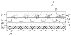
- FIG. 1 is a cross-sectional view of the solid-state imaging device according to the first embodiment of the present invention.
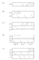
- 2A to 2E are cross-sectional views showing the method of manufacturing the solid-state imaging device according to the first embodiment of the present invention in the order of steps.
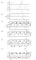
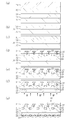
- 3A to 3F are cross-sectional views showing the method of manufacturing the solid-state imaging device according to the first embodiment of the present invention in the order of steps.
- 4A to 4E are cross-sectional views showing a method of manufacturing a solid-state imaging device according to the second embodiment of the present invention in the order of steps.
- FIG. 5A to FIG. 5G are cross-sectional views showing a method of manufacturing a solid-state imaging device according to the second embodiment of the present invention in the order of steps.
- FIGS. 6A to 6E are cross-sectional views showing a method of manufacturing a solid-state imaging device according to the third embodiment of the present invention in the order of steps.
- 7A to 7F are cross-sectional views showing the method of manufacturing the solid-state imaging device according to the first embodiment of the present invention in the order of steps.
- FIG. 8 is a schematic diagram showing fixed pattern noise due to activation spots of laser annealing.
- FIG. 9 is a schematic diagram showing impurity concentration spots of a semiconductor wafer manufactured by a conventional CZ method.
- 10 (a) to 10 (e) are cross-sectional views showing a method of manufacturing a back-illuminated solid-state imaging device using a conventional SOI wafer in the order of steps.
- FIG. 11 (a) to 11 (e) are cross-sectional views showing a method of manufacturing a back-illuminated solid-state imaging device using a conventional SOI wafer in the order of steps.
- FIG. 12 is a schematic diagram showing fixed pattern noise of a back-illuminated solid-state imaging device using a conventional SOI wafer.
- FIG. 1 shows a cross-sectional structure of a solid-state imaging device according to the first embodiment of the present invention.
- the solid-state imaging device includes a silicon single crystal layer 24 formed by an epitaxial method and a silicon oxide layer 22 having a surface formed by heat treatment.
- the silicon single crystal layer 24 is made p-type by introducing impurities so as to become the p-well 21.
- a photodiode 19 and a drain 26 are formed in the silicon single crystal layer 24, and a readout gate 25 and a wiring 27 are formed on the silicon single crystal layer 24.
- An interlayer insulating film 34 is formed on the silicon single crystal layer 24 so as to cover the read gate 25 and the wiring 27.
- the photodiode 19 is formed by forming an n-type region by ion implantation of arsenic, phosphorus, antimony or the like. The light receiving portion of the photodiode 19 is formed to face the silicon oxide layer 22.
- a p + -type depletion preventing layer 28 is formed under the silicon single crystal layer 24 by implanting, for example, boron (B) ions from the surface on which the silicon oxide layer 22 is formed.
- B boron
- the impurity concentration of the depletion preventing layer 28 varies depending on the impurity concentration of the photodiode 19, it is usually preferably 1 ⁇ 10 17 cm ⁇ 3 or more and 1 ⁇ 10 19 cm ⁇ 3 or less. In this case, since the depletion layer of the photodiode 19 does not extend to the interface with the silicon oxide layer 22, it is effective for suppressing dark signals generated by accumulation of noise electrons generated at the interface state in the photodiode 19. is there.
- a color filter 29 is formed on the surface of the silicon oxide layer 22 opposite to the silicon single crystal layer 24, and an on-chip microlens 30 is formed on the color filter 29.
- the solid-state imaging device does not include a silicon single crystal formed by the Czochralski (CZ) method, which cannot avoid concentric spots of impurity concentration, thereby preventing generation of fixed pattern noise and improving image quality. can do.
- CZ Czochralski
- FIGS. 2 (a) to 2 (e) and FIGS. 3 (a) to 3 (f) show the manufacturing method of the solid-state imaging device according to the first embodiment of the present invention in the order of steps.
- a bond wafer 20 that is a silicon single crystal is prepared.
- the conductivity type and impurity concentration of the bond wafer 20 are not directly related to the p-well 21 of the completed solid-state imaging device 18 shown in FIG. 2 and 3, the bond wafer 20 is shown so that the main surface is on the lower side.
- the bond wafer 20 may use a silicon single crystal manufactured by the CZ method.
- a silicon single crystal layer 24 into which a p-type impurity is introduced is deposited on the main surface of the bond wafer 20 by an epitaxial method.
- the silicon single crystal layer 24 must be equal to or greater than the thickness of the substrate on which the solid-state imaging device is finally formed.
- a film thickness of a substrate of several ⁇ m to 10 ⁇ m is required. Therefore, a deposited film thickness of the silicon single crystal layer 24 by the epitaxial method is also required to be several ⁇ m to 10 ⁇ m.
- the silicon oxide layer 22 is formed by thermally oxidizing the bond wafer 20. Although the formed silicon oxide layer 22 is shown only on the front surface (lower surface) side, the silicon oxide layer 22 is actually formed also on the back surface and the side surface of the bond wafer 20.
- a defect layer 23 is formed inside the silicon single crystal layer 24 by implanting hydrogen ions into the silicon single crystal layer 24 from the silicon oxide layer 22 side. After bonding the bond wafer 20 and the base wafer 17, the bond wafer 20 is peeled off at the defect layer 23. Therefore, the thickness of the silicon single crystal layer 24 in the SOI (Silicon-On-Insulator) wafer can be determined by adjusting the ion implantation depth by controlling the acceleration energy at the time of hydrogen ion implantation. Therefore, in the present embodiment, the depth of the defect layer 23 is the film thickness of the silicon single crystal that finally forms the solid-state imaging device 18.
- SOI Silicon-On-Insulator
- the film thickness is about several ⁇ m to 10 ⁇ m as described above. Since the deposited film thickness of the silicon single crystal layer 24 by the epitaxial method shown in FIG. 2B is larger than the film thickness of the silicon single crystal forming the solid-state imaging device 18, the defect layer 23 caused by hydrogen ion implantation is It is formed in the silicon single crystal layer 24 by the epitaxial method.
- a base wafer 17 for maintaining the strength of the SOI wafer 16 completed in FIG. 3 (b) is prepared, and the prepared base wafer 17, the silicon single crystal layer 24, Then, the surfaces of the base wafer 17 and the silicon single crystal layer 24 are bonded to each other. At this time, by simply pressing the base wafer 17 and the bond wafer 20 on which the silicon single crystal layer 24 is deposited, the flatness of each is sufficiently high.
- the cleaning process not only removes contaminants and particles, but also has the purpose of enhancing the adhesion effect by making each surface hydrophilic.
- the base wafer 17 may be a silicon single crystal manufactured by the CZ method.
- the base wafer 17 is shown as being thinner than the bond wafer 20, this is for convenience, and the base wafer 17 must have a film thickness that can maintain the strength as the SOI wafer 16. Therefore, when the diameter is 200 mm or more, a film thickness of 500 ⁇ m or more is usually required.
- the bond wafer 20 also needs to have the same film thickness as that of the base wafer 17 in order to go through the process up to the bonding with the base wafer 17.
- the silicon single crystal layer 24 is peeled off from the defect layer 23.
- part of the bond wafer 20 and the silicon single crystal layer 24 peeled off from the base wafer 17 is returned to the epitaxial growth step of FIG. 2B, and may be reused for manufacturing another SOI wafer.
- heat treatment is performed to strengthen the adhesion between the bonded surfaces.
- the temperature of this heat treatment is 400 ° C. or higher, preferably about 1000 ° C., considering the adhesive strength.
- the SOI wafer 16 composed of the base wafer 17, the silicon oxide layer 22, and the silicon single crystal layer 24 is completed by the above process.
- the silicon single crystal layer 24 is entirely formed by the epitaxial method, the impurity concentration unevenness is extremely small as compared with the conventional silicon single crystal layer formed by the CZ method. Is the feature.
- the photodiode 19 and the drain 26 are formed in the silicon single crystal layer 24, and the read gate 25 and the wiring 27 are formed on the silicon single crystal layer 24.
- a MOS type solid-state imaging device is formed.
- a charge-coupled device (CCD) type solid-state imaging device a photodiode, a charge transfer unit, a gate electrode, and a wiring replace this.
- an n-type region is formed by ion implantation of an impurity such as arsenic, phosphorus, or antimony to form the photodiode 19.
- an interlayer insulating film 34 is formed on the silicon single crystal layer 24 so as to cover the read gate 25 and the wiring 27.
- the p-type silicon single crystal layer 24 is formed by the epitaxial method in FIG. 2B, but this is n-type, and ion implantation is performed in the step shown in FIG. 3C.
- the p-well 21 may be formed by, for example, and the photodiode 19 may be formed in the formed p-well 21.
- the base wafer 17 is removed. It is efficient to perform etching with an alkaline solution after removing most of it by polishing, dry etching or the like. However, only etching with an alkaline solution may be used. Since the base wafer 17 is a silicon single crystal, it can be easily removed by etching with an alkaline solution, and since the intermediate silicon oxide layer 22 is not etched with an alkaline solution, it serves as an etching stopper, and the film of the SOI wafer 16 Thin film processing can be performed with high accuracy, whose thickness is mainly determined by the depth of hydrogen ion implantation.
- the film thickness accuracy is greatly increased. Is the advantage.
- the removal of the base wafer 17 may be limited to the light receiving region of the solid-state imaging device 18 using a mask process.
- the base wafer 17 is removed from the entire surface of the SOI wafer 16, the strength of the entire wafer is insufficient. Therefore, it is desirable to reinforce by attaching a quartz wafer or the like as a support wafer in advance on the surface side on which the wiring 27 and the like are formed. . However, it is omitted here. In the present embodiment, only the base wafer 17 is removed.
- the silicon oxide layer 22 is selectively removed by etching with an acid after the base wafer 17 is removed with an alkaline solution or the like, the film is removed.
- the thickness processing accuracy does not change, and the effect of using the SOI wafer 16 can be obtained.
- boron ions are implanted from the surface on which the silicon oxide layer 22 is formed, and in the vicinity of the interface between the silicon single crystal layer 24 and the silicon oxide 22 layer in the silicon single crystal layer 24. Then, a p + type depletion prevention layer 28 is formed.
- concentration of the depletion preventing layer 28 varies depending on the impurity concentration of the photodiode 19, it is usually preferably 1 ⁇ 10 17 cm ⁇ 3 or more and 1 ⁇ 10 19 cm ⁇ 3 or less.
- the depletion layer of the photodiode 19 extends to the interface with the silicon oxide layer 22, and noise electrons generated at the interface state can be prevented from accumulating in the photodiode 19 and becoming a dark signal. .
- the basic function as an imaging device can be obtained although the image quality is lowered.
- a color filter 29 and an on-chip microlens 30 are formed on the silicon oxide layer 22 as necessary, and only the silicon single crystal layer 24 is formed by an epitaxial method.
- the back-illuminated solid-state imaging device 18 thus completed is completed.
- the manufacturing method of the solid-state imaging device according to this embodiment can form a solid-state imaging device 18 that does not include a silicon single crystal formed by the CZ method in which concentric spots of impurity concentration cannot be avoided. It is possible to manufacture a solid-state imaging device that does not generate such fixed pattern noise.
- the back-illuminated solid-state imaging device has been described.
- a conventional front-side solid-state imaging device can be similarly manufactured using an SOI wafer. Thinning the light receiving region with a surface-type solid-state imaging device is effective, for example, when giving sensitivity only to a specific short wavelength, or when using light transmitted through the solid-state imaging device for some purpose.
- the depletion prevention layer 28 shown in FIG. 3 (e) needs to be formed by implanting boron ions into the opposite surface of the silicon single crystal layer 24, as shown in FIG. 3 (d). In the process.
- the manufacturing method is shown by taking the MOS type solid-state imaging device as an example, but a similar manufacturing method using an SOI wafer can be applied to the CCD type solid-state imaging device.
- the manufacturing method of the solid-state imaging device of the present invention can be applied to other conductive types.
- FIGS. 5 (a) to 5 (g) show a manufacturing method of the solid-state imaging device according to the second embodiment of the present invention in the order of steps.
- the silicon single crystal layer 24 in the first embodiment is the first silicon single crystal layer 32 in the present embodiment.
- a second silicon single crystal layer 31 is deposited on the first silicon single crystal layer 32 by an epitaxial method.
- a p-type impurity is introduced into the second silicon single crystal layer 31.
- the total thickness of the peeled first silicon single crystal layer 32 and second silicon single crystal layer 31 is the substrate thickness of the solid-state imaging device 18 shown in FIG.
- the film thickness of the substrate needs to be about several ⁇ m to 10 ⁇ m. Therefore, when the depth of the defect layer 23 in the first silicon single crystal layer 32 is d1, and the film thickness of the second silicon single crystal layer 31 deposited in FIG. 5C is d2, d1 + d2 and the target It is necessary to make the film thickness of the substrate of the solid-state imaging device 18 equal.
- the photodiode 19 and the drain 26 are formed in the second silicon single crystal layer 31, and the read gate 25 and the wiring 27 are formed on the second silicon single crystal layer 31.
- a MOS type solid-state imaging device is formed.
- a photodiode, a charge transfer unit, a gate electrode, and wiring replace this.
- an n-type region is formed by ion implantation of an impurity such as arsenic, phosphorus, or antimony in forming the photodiode 19. .
- an interlayer insulating film 34 is formed on the silicon single crystal layer 24 so as to cover the read gate 25 and the wiring 27.
- an n-type second silicon single crystal layer 31 is formed by an epitaxial method, and a p-well 21 is formed in the formed second silicon single crystal layer 31 by ion implantation or the like.
- a photodiode 19 or the like may be formed in the well 21.
- the base wafer 17 is removed. It is efficient to perform etching with an alkaline solution after removing most of it by polishing, dry etching or the like. However, only etching with an alkaline solution may be used. Since the base wafer 17 is a single crystal of silicon, it can be easily removed by etching with an alkaline solution, and the intermediate silicon oxide layer 22 is not etched with an alkaline solution, so that it serves as an etching stopper, and the film thickness of the SOI wafer 16 is reduced. However, it is possible to process a thin film with high accuracy determined mainly by the depth of hydrogen ion implantation.
- the film thickness accuracy is greatly increased. Is the advantage.
- the removal of the base wafer 17 may be limited to the light receiving region of the solid-state imaging device 18 using a mask process.
- the base wafer 17 is removed from the entire surface of the SOI wafer 16, the strength of the entire wafer is insufficient. Therefore, it is desirable to reinforce by attaching a quartz wafer or the like as a support wafer in advance on the surface side on which the wiring 27 and the like are formed. . However, it is omitted here. In the present embodiment, only the base wafer 17 is removed.
- the silicon oxide layer 22 is selectively removed by etching with an acid after the base wafer 17 is removed with an alkaline solution or the like, the film is removed.
- the thickness processing accuracy does not change, and the effect of using the SOI wafer 16 can be obtained.
- a p + type depletion preventing layer 28 is formed in the vicinity of the interface with the silicon layer 22.
- concentration of the depletion preventing layer 28 varies depending on the impurity concentration of the photodiode 19, it is usually preferably 1 ⁇ 10 17 cm ⁇ 3 or more and 1 ⁇ 10 19 cm ⁇ 3 or less.
- the depletion layer of the photodiode 19 extends to the interface with the silicon oxide layer 22, and noise electrons generated at the interface level are accumulated in the photodiode 19, thereby suppressing dark signals.
- this step is omitted, the basic function as an imaging device can be obtained although the image quality is lowered.
- a color filter 29 and an on-chip microlens 30 are formed on the silicon oxide layer 22 as necessary, and the first silicon single crystal layer 32 is formed by an epitaxial method. And the backside illumination type solid-state imaging device 18 formed only by the second silicon single crystal layer 31 is completed.
- the manufacturing method of the solid-state imaging device according to this embodiment can form a solid-state imaging device 18 that does not include a silicon single crystal formed by the CZ method in which concentric spots of impurity concentration cannot be avoided. It is possible to manufacture a solid-state imaging device that does not generate such fixed pattern noise.
- the SOI wafer 16 is formed by the hydrogen ion peeling method, but a large number of defect layers 23 are left on the peeling surface by the hydrogen ion implantation. Therefore, when the read gate 25, the drain 26, the wiring 27, and the like are formed on the separation surface by hydrogen ion implantation, the read gate 25 has a threshold voltage variation due to an increase in the interface state, the drain 26 has a dark output increase, and the wiring 27
- the solid-state imaging device may cause image quality deterioration due to an increase in noise or the like.
- the second silicon single crystal layer 31 is formed on the first silicon single crystal 32 having a large number of defect layers 23 remaining on the surface, the readout gate 25, the drain 26, and the The wiring 27 and the like can be formed on the surface of the second silicon single crystal layer 31 having no defect. Therefore, the image quality of the imaging device can be improved.
- epitaxial growth of single crystal silicon is usually performed at a high temperature of 1000 ° C. or higher using a silane-based source gas, hydrogen atoms ion-implanted from the silicon oxide layer 22 side into the first silicon single crystal layer 32 are removed. And has the effect of recovering defects caused by ion implantation.
- the boundary surface between the first silicon single crystal layer 32 and the second silicon single crystal layer 31 is not present in the depletion layer of the photodiode 19. This is because crystal defects remaining inside the photodiode 19 become a source of dark current and cause fixed pattern noise called white spots.
- the first silicon single crystal layer 32 and the second silicon are separated by setting the film thickness d1 of the first silicon single crystal layer 32 after peeling to be equal to or less than the thickness of the depletion prevention layer 28.
- the boundary surface with the single crystal layer 31 can be positioned inside the depletion prevention layer 28, and the boundary surface between the first silicon single crystal layer 32 and the second silicon single crystal layer 31 is depleted in the photodiode 19. It can be a structure that does not exist in the layer. With such a configuration, the image quality of the solid-state imaging device can be further improved.
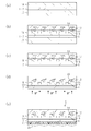
- FIGS. 7 (a) to 7 (f) show a method of manufacturing the solid-state imaging device according to the third embodiment of the present invention in the order of steps.
- FIG. 8 is a schematic diagram showing fixed pattern noise due to activation spots of laser annealing.
- the silicon single crystal layer 32 in the second embodiment is the first depletion prevention silicon single crystal layer 33 in this embodiment, and the conductivity type and impurity concentration are the depletion prevention layer in FIG. 28, that is, a p + type silicon single crystal of 1 ⁇ 10 17 cm ⁇ 3 or more and 1 ⁇ 10 19 cm ⁇ 3 or less.
- the depth of the defect layer 23 formed by hydrogen ion implantation is set to the thickness of the depletion prevention layer 28 in the first embodiment and the second embodiment. By making them substantially equal, the first depletion prevention silicon single crystal layer 33 functions as the depletion prevention layer 28 in the first and second embodiments, so that the B + ion implantation step is not required. The point is different.
- the color filter 29 is formed on the silicon oxide layer 22 as necessary. Then, the on-chip microlens 30 and the like are formed, and the back-illuminated solid-state imaging device 18 formed of only a silicon single crystal by epitaxial growth is completed.
- activation annealing In order for a silicon single crystal to exhibit a desired electrical conductivity by implantation of impurity ions such as boron, it is necessary to arrange impurity atoms at a stable position in the silicon single crystal by a heat treatment generally called activation annealing. .
- This activation annealing usually needs to be performed by heat treatment at 800 ° C. or higher.
- the wiring 27 may be formed of a metal such as aluminum or copper. Therefore, the temperature applied to the entire wafer takes into account the melting point of the wiring 27. It must be done and it is difficult to heat above 500 ° C. As a result, only a part of the ion-implanted impurities can be activated.
- a heating method called laser annealing can be used.
- This is a method in which a wafer is scanned with a powerful laser beam to heat the entire surface of the wafer, and one surface of the wafer can be locally heated.
- this method also has two problems.
- the first problem is heating spots caused by scanning with laser light.
- the diameter of the laser beam is several hundred ⁇ m to several mm at the maximum, and is smaller than the solid-state imaging device and larger than the pixel size.
- the heating spots resulting from the scanning of the laser beam become the spots for activating the impurities, causing spots of the conductive properties.
- the second problem is that since the thickness of the region where the photodiode 19 is formed is several ⁇ m to 10 ⁇ m, even when laser light is irradiated from the back surface of the SOI wafer 16, the surface (upper surface) of the wafer 16 is exposed. ) Side is also hot.
- an advantage of the backside illumination type solid-state imaging device is that the layout of the wiring 27 on the front surface side is not restricted by the pixel arrangement.
- the temperature of the part irradiated with the reflected light rises more than the other part. For this reason, there is a possibility that an impurity activation spot reflecting the layout of the wiring 27 may occur, and there is a concern about the generation of fixed pattern noise different from the scanning spot.
- the above problem may be improved if a laser annealing technique with a short wavelength is developed, but the heat treatment during the back surface processing is an essential problem of the back side illumination type solid-state imaging device.
- the manufacturing method of the solid-state imaging device it is not necessary to perform the activation annealing by forming the depletion prevention layer 28 by ion implantation after the formation of the read gate 25 and the wiring 27, and this is caused by the activation annealing.
- the generation of fixed pattern noise can be avoided.
- the impurity concentration of the first depletion-preventing silicon single crystal layer 33 is sufficient, depletion occurs at the boundary surface between the first depletion-preventing silicon single crystal layer 33 and the second silicon single crystal layer 31. It does not occur and the boundary surface is not included in the photodiode 19. For this reason, no white defect occurs and a good image quality can be obtained.
- the second silicon single crystal layer 31 is p-type and the photodiode 19 is n-type.
- the second silicon single crystal layer 31 may be n-type.
- a p-well may be formed in the second silicon single crystal layer 31 by ion implantation or the like, and the n-type photodiode 19 may be formed in the formed p-well.
- the solid-state imaging device and the manufacturing method thereof according to the present invention can prevent a fixed pattern noise because a solid-state imaging device not including a silicon single crystal formed by a CZ method in which concentric spots of impurity concentration cannot be avoided can be formed.
- a solid-state imaging device using an SOI substrate, a manufacturing method thereof, and the like.
Landscapes
- Solid State Image Pick-Up Elements (AREA)
- Engineering & Computer Science (AREA)
- Manufacturing & Machinery (AREA)
- Transforming Light Signals Into Electric Signals (AREA)
Priority Applications (3)
| Application Number | Priority Date | Filing Date | Title |
|---|---|---|---|
| US13/220,079 US20110316107A1 (en) | 2009-03-18 | 2011-08-29 | Solid-state image sensor and manufacturing method of the sensor |
| US14/061,750 US9018031B2 (en) | 2009-03-18 | 2013-10-23 | Manufacturing method of solid-state image sensor |
| US15/582,014 USRE47208E1 (en) | 2009-03-18 | 2017-04-28 | Manufacturing method of solid-state image sensor |
Applications Claiming Priority (2)
| Application Number | Priority Date | Filing Date | Title |
|---|---|---|---|
| JP2009066877A JP5356872B2 (ja) | 2009-03-18 | 2009-03-18 | 個体撮像装置の製造方法 |
| JP2009-066877 | 2009-03-18 |
Related Child Applications (1)
| Application Number | Title | Priority Date | Filing Date |
|---|---|---|---|
| US13/220,079 Continuation US20110316107A1 (en) | 2009-03-18 | 2011-08-29 | Solid-state image sensor and manufacturing method of the sensor |
Publications (1)
| Publication Number | Publication Date |
|---|---|
| WO2010106591A1 true WO2010106591A1 (ja) | 2010-09-23 |
Family
ID=42739265
Family Applications (1)
| Application Number | Title | Priority Date | Filing Date |
|---|---|---|---|
| PCT/JP2009/005509 Ceased WO2010106591A1 (ja) | 2009-03-18 | 2009-10-21 | 固体撮像装置及びその製造方法 |
Country Status (3)
| Country | Link |
|---|---|
| US (3) | US20110316107A1 (enExample) |
| JP (1) | JP5356872B2 (enExample) |
| WO (1) | WO2010106591A1 (enExample) |
Families Citing this family (11)
| Publication number | Priority date | Publication date | Assignee | Title |
|---|---|---|---|---|
| JP2013149712A (ja) | 2012-01-18 | 2013-08-01 | Toshiba Corp | 半導体装置の製造方法 |
| US8871608B2 (en) * | 2012-02-08 | 2014-10-28 | Gtat Corporation | Method for fabricating backside-illuminated sensors |
| JP6032963B2 (ja) * | 2012-06-20 | 2016-11-30 | キヤノン株式会社 | Soi基板、soi基板の製造方法および半導体装置の製造方法 |
| JP2014027123A (ja) * | 2012-07-27 | 2014-02-06 | Renesas Electronics Corp | 半導体装置およびその製造方法 |
| US9490128B2 (en) * | 2012-08-27 | 2016-11-08 | Ultratech, Inc. | Non-melt thin-wafer laser thermal annealing methods |
| JP2014086553A (ja) * | 2012-10-23 | 2014-05-12 | Toshiba Corp | 固体撮像装置および固体撮像装置の製造方法 |
| JP6118757B2 (ja) * | 2014-04-24 | 2017-04-19 | 信越半導体株式会社 | 貼り合わせsoiウェーハの製造方法 |
| JP6100200B2 (ja) * | 2014-04-24 | 2017-03-22 | 信越半導体株式会社 | 貼り合わせsoiウェーハの製造方法 |
| JP6598436B2 (ja) * | 2014-08-08 | 2019-10-30 | キヤノン株式会社 | 光電変換装置、撮像システム、及び光電変換装置の製造方法 |
| US10083843B2 (en) | 2014-12-17 | 2018-09-25 | Ultratech, Inc. | Laser annealing systems and methods with ultra-short dwell times |
| FR3083000B1 (fr) * | 2018-06-21 | 2024-11-29 | Soitec Silicon On Insulator | Substrat pour capteur d'image de type face avant et procede de fabrication d'un tel substrat |
Citations (3)
| Publication number | Priority date | Publication date | Assignee | Title |
|---|---|---|---|---|
| JPH10308355A (ja) * | 1997-05-09 | 1998-11-17 | Denso Corp | 半導体基板の製造方法 |
| JPH10321548A (ja) * | 1997-05-15 | 1998-12-04 | Denso Corp | 半導体基板の製造方法 |
| JP2008103668A (ja) * | 2006-09-20 | 2008-05-01 | Fujifilm Corp | 裏面照射型撮像素子及びこれを備えた撮像装置 |
Family Cites Families (26)
| Publication number | Priority date | Publication date | Assignee | Title |
|---|---|---|---|---|
| EP0387754A1 (de) | 1989-03-17 | 1990-09-19 | Schott Glaswerke | Kathetersystem zur Uebertragung von Laserstrahlung in Gefaesssysteme des menschlichen Koerpers |
| FR2681472B1 (fr) | 1991-09-18 | 1993-10-29 | Commissariat Energie Atomique | Procede de fabrication de films minces de materiau semiconducteur. |
| JP3438369B2 (ja) * | 1995-01-17 | 2003-08-18 | ソニー株式会社 | 部材の製造方法 |
| JP2959704B2 (ja) | 1995-03-27 | 1999-10-06 | 信越半導体株式会社 | 結合ウェーハの製造方法及びこの方法により製造された結合ウェーハ |
| US6251754B1 (en) | 1997-05-09 | 2001-06-26 | Denso Corporation | Semiconductor substrate manufacturing method |
| JPH11307747A (ja) * | 1998-04-17 | 1999-11-05 | Nec Corp | Soi基板およびその製造方法 |
| JP3385972B2 (ja) | 1998-07-10 | 2003-03-10 | 信越半導体株式会社 | 貼り合わせウェーハの製造方法および貼り合わせウェーハ |
| FR2781929B1 (fr) * | 1998-07-28 | 2002-08-30 | St Microelectronics Sa | Capteur d'image a reseau de photodiodes |
| JP4228419B2 (ja) | 1998-07-29 | 2009-02-25 | 信越半導体株式会社 | Soiウエーハの製造方法およびsoiウエーハ |
| US6979588B2 (en) * | 2003-01-29 | 2005-12-27 | Hynix Semiconductor Inc. | Method for manufacturing CMOS image sensor having microlens therein with high photosensitivity |
| JP4046069B2 (ja) * | 2003-11-17 | 2008-02-13 | ソニー株式会社 | 固体撮像素子及び固体撮像素子の製造方法 |
| JP4181487B2 (ja) * | 2003-11-28 | 2008-11-12 | 松下電器産業株式会社 | 固体撮像装置とその製造方法 |
| JP2005259828A (ja) | 2004-03-10 | 2005-09-22 | Sony Corp | 固体撮像素子及びその製造方法 |
| US7335963B2 (en) * | 2004-08-25 | 2008-02-26 | Micron Technology, Inc. | Light block for pixel arrays |
| US7425460B2 (en) * | 2004-09-17 | 2008-09-16 | California Institute Of Technology | Method for implementation of back-illuminated CMOS or CCD imagers |
| US7202543B2 (en) * | 2005-03-07 | 2007-04-10 | Micron Technology, Inc. | Method and structure to reduce optical crosstalk in a solid state imager |
| US7919827B2 (en) * | 2005-03-11 | 2011-04-05 | Taiwan Semiconductor Manufacturing Co., Ltd. | Method and structure for reducing noise in CMOS image sensors |
| KR100710204B1 (ko) * | 2005-09-08 | 2007-04-20 | 동부일렉트로닉스 주식회사 | 씨모스 이미지 센서 및 그 제조방법 |
| US7777287B2 (en) * | 2006-07-12 | 2010-08-17 | Micron Technology, Inc. | System and apparatus providing analytical device based on solid state image sensor |
| US7781715B2 (en) * | 2006-09-20 | 2010-08-24 | Fujifilm Corporation | Backside illuminated imaging device, semiconductor substrate, imaging apparatus and method for manufacturing backside illuminated imaging device |
| KR100829378B1 (ko) * | 2006-12-27 | 2008-05-13 | 동부일렉트로닉스 주식회사 | 이미지 센서 및 이의 제조 방법 |
| US20090200631A1 (en) * | 2008-02-08 | 2009-08-13 | Omnivision Technologies, Inc. | Backside illuminated imaging sensor with light attenuating layer |
| JP5288823B2 (ja) * | 2008-02-18 | 2013-09-11 | キヤノン株式会社 | 光電変換装置、及び光電変換装置の製造方法 |
| US7968923B2 (en) * | 2008-03-12 | 2011-06-28 | Omnivision Technologies, Inc. | Image sensor array with conformal color filters |
| JP5269454B2 (ja) * | 2008-03-25 | 2013-08-21 | 株式会社東芝 | 固体撮像素子 |
| US8211732B2 (en) * | 2008-09-11 | 2012-07-03 | Omnivision Technologies, Inc. | Image sensor with raised photosensitive elements |
-
2009
- 2009-03-18 JP JP2009066877A patent/JP5356872B2/ja active Active
- 2009-10-21 WO PCT/JP2009/005509 patent/WO2010106591A1/ja not_active Ceased
-
2011
- 2011-08-29 US US13/220,079 patent/US20110316107A1/en not_active Abandoned
-
2013
- 2013-10-23 US US14/061,750 patent/US9018031B2/en not_active Ceased
-
2017
- 2017-04-28 US US15/582,014 patent/USRE47208E1/en active Active
Patent Citations (3)
| Publication number | Priority date | Publication date | Assignee | Title |
|---|---|---|---|---|
| JPH10308355A (ja) * | 1997-05-09 | 1998-11-17 | Denso Corp | 半導体基板の製造方法 |
| JPH10321548A (ja) * | 1997-05-15 | 1998-12-04 | Denso Corp | 半導体基板の製造方法 |
| JP2008103668A (ja) * | 2006-09-20 | 2008-05-01 | Fujifilm Corp | 裏面照射型撮像素子及びこれを備えた撮像装置 |
Also Published As
| Publication number | Publication date |
|---|---|
| USRE47208E1 (en) | 2019-01-15 |
| US20140051203A1 (en) | 2014-02-20 |
| US9018031B2 (en) | 2015-04-28 |
| JP2010219439A (ja) | 2010-09-30 |
| JP5356872B2 (ja) | 2013-12-04 |
| US20110316107A1 (en) | 2011-12-29 |
Similar Documents
| Publication | Publication Date | Title |
|---|---|---|
| JP5356872B2 (ja) | 個体撮像装置の製造方法 | |
| US7843027B2 (en) | Solid-state imaging device, camera and method of producing the solid-state imaging device | |
| JP5347520B2 (ja) | 固体撮像装置の製造方法 | |
| TWI375320B (en) | Image sensor and manufacturing method thereof | |
| TW201027737A (en) | Technique for fabrication of backside illuminated image sensor | |
| JP2010503991A (ja) | 薄膜soiを用いるイメージセンサ | |
| CN101800232B (zh) | 固态摄像装置及其制作方法、摄像设备、半导体装置及其制作方法以及半导体衬底 | |
| JP5481419B2 (ja) | 半導体装置の製造方法 | |
| JP4997879B2 (ja) | 半導体装置及びその製造方法並びに固体撮像装置及びその製造方法並びに撮像装置 | |
| TW201238041A (en) | Solid-state imaging device and manufacturing method of solid-state imaging device | |
| US20090179295A1 (en) | Image sensor and method for manufacturing the same | |
| TW200929531A (en) | Image sensor and method for manufacturing the same | |
| US20090179242A1 (en) | Image sensor and method for manufacturing the same | |
| US8222587B2 (en) | Image sensor and method for manufacturing the same | |
| JP2008294479A (ja) | 固体撮像装置 | |
| US20100093128A1 (en) | Method for manufacturing image sensor | |
| JP2006041117A (ja) | 固体撮像素子の製造方法 | |
| JPH0613387A (ja) | 固体撮像装置 | |
| JP2010067735A (ja) | 固体撮像装置の製造方法および固体撮像装置の基板の製造方法 | |
| KR20100050725A (ko) | 이미지 센서의 제조 방법 |
Legal Events
| Date | Code | Title | Description |
|---|---|---|---|
| 121 | Ep: the epo has been informed by wipo that ep was designated in this application |
Ref document number: 09841799 Country of ref document: EP Kind code of ref document: A1 |
|
| NENP | Non-entry into the national phase |
Ref country code: DE |
|
| 122 | Ep: pct application non-entry in european phase |
Ref document number: 09841799 Country of ref document: EP Kind code of ref document: A1 |