WO2010100726A1 - プリント基板モジュール - Google Patents
プリント基板モジュール Download PDFInfo
- Publication number
- WO2010100726A1 WO2010100726A1 PCT/JP2009/054049 JP2009054049W WO2010100726A1 WO 2010100726 A1 WO2010100726 A1 WO 2010100726A1 JP 2009054049 W JP2009054049 W JP 2009054049W WO 2010100726 A1 WO2010100726 A1 WO 2010100726A1
- Authority
- WO
- WIPO (PCT)
- Prior art keywords
- circuit board
- printed circuit
- pedestal
- side wall
- top plate
- Prior art date
Links
Images


Classifications
-
- H—ELECTRICITY
- H05—ELECTRIC TECHNIQUES NOT OTHERWISE PROVIDED FOR
- H05K—PRINTED CIRCUITS; CASINGS OR CONSTRUCTIONAL DETAILS OF ELECTRIC APPARATUS; MANUFACTURE OF ASSEMBLAGES OF ELECTRICAL COMPONENTS
- H05K1/00—Printed circuits
- H05K1/02—Details
- H05K1/03—Use of materials for the substrate
-
- H—ELECTRICITY
- H05—ELECTRIC TECHNIQUES NOT OTHERWISE PROVIDED FOR
- H05K—PRINTED CIRCUITS; CASINGS OR CONSTRUCTIONAL DETAILS OF ELECTRIC APPARATUS; MANUFACTURE OF ASSEMBLAGES OF ELECTRICAL COMPONENTS
- H05K1/00—Printed circuits
- H05K1/02—Details
- H05K1/14—Structural association of two or more printed circuits
-
- H—ELECTRICITY
- H05—ELECTRIC TECHNIQUES NOT OTHERWISE PROVIDED FOR
- H05K—PRINTED CIRCUITS; CASINGS OR CONSTRUCTIONAL DETAILS OF ELECTRIC APPARATUS; MANUFACTURE OF ASSEMBLAGES OF ELECTRICAL COMPONENTS
- H05K3/00—Apparatus or processes for manufacturing printed circuits
- H05K3/36—Assembling printed circuits with other printed circuits
- H05K3/366—Assembling printed circuits with other printed circuits substantially perpendicularly to each other
-
- H—ELECTRICITY
- H01—ELECTRIC ELEMENTS
- H01L—SEMICONDUCTOR DEVICES NOT COVERED BY CLASS H10
- H01L2924/00—Indexing scheme for arrangements or methods for connecting or disconnecting semiconductor or solid-state bodies as covered by H01L24/00
- H01L2924/15—Details of package parts other than the semiconductor or other solid state devices to be connected
- H01L2924/151—Die mounting substrate
- H01L2924/1515—Shape
- H01L2924/15158—Shape the die mounting substrate being other than a cuboid
- H01L2924/15162—Top view
-
- H—ELECTRICITY
- H05—ELECTRIC TECHNIQUES NOT OTHERWISE PROVIDED FOR
- H05K—PRINTED CIRCUITS; CASINGS OR CONSTRUCTIONAL DETAILS OF ELECTRIC APPARATUS; MANUFACTURE OF ASSEMBLAGES OF ELECTRICAL COMPONENTS
- H05K1/00—Printed circuits
- H05K1/02—Details
- H05K1/14—Structural association of two or more printed circuits
- H05K1/141—One or more single auxiliary printed circuits mounted on a main printed circuit, e.g. modules, adapters
-
- H—ELECTRICITY
- H05—ELECTRIC TECHNIQUES NOT OTHERWISE PROVIDED FOR
- H05K—PRINTED CIRCUITS; CASINGS OR CONSTRUCTIONAL DETAILS OF ELECTRIC APPARATUS; MANUFACTURE OF ASSEMBLAGES OF ELECTRICAL COMPONENTS
- H05K2201/00—Indexing scheme relating to printed circuits covered by H05K1/00
- H05K2201/10—Details of components or other objects attached to or integrated in a printed circuit board
- H05K2201/10227—Other objects, e.g. metallic pieces
- H05K2201/1034—Edge terminals, i.e. separate pieces of metal attached to the edge of the PCB
-
- H—ELECTRICITY
- H05—ELECTRIC TECHNIQUES NOT OTHERWISE PROVIDED FOR
- H05K—PRINTED CIRCUITS; CASINGS OR CONSTRUCTIONAL DETAILS OF ELECTRIC APPARATUS; MANUFACTURE OF ASSEMBLAGES OF ELECTRICAL COMPONENTS
- H05K2201/00—Indexing scheme relating to printed circuits covered by H05K1/00
- H05K2201/10—Details of components or other objects attached to or integrated in a printed circuit board
- H05K2201/10227—Other objects, e.g. metallic pieces
- H05K2201/10424—Frame holders
-
- H—ELECTRICITY
- H05—ELECTRIC TECHNIQUES NOT OTHERWISE PROVIDED FOR
- H05K—PRINTED CIRCUITS; CASINGS OR CONSTRUCTIONAL DETAILS OF ELECTRIC APPARATUS; MANUFACTURE OF ASSEMBLAGES OF ELECTRICAL COMPONENTS
- H05K2201/00—Indexing scheme relating to printed circuits covered by H05K1/00
- H05K2201/10—Details of components or other objects attached to or integrated in a printed circuit board
- H05K2201/10613—Details of electrical connections of non-printed components, e.g. special leads
- H05K2201/10954—Other details of electrical connections
- H05K2201/10962—Component not directly connected to the PCB
-
- H—ELECTRICITY
- H05—ELECTRIC TECHNIQUES NOT OTHERWISE PROVIDED FOR
- H05K—PRINTED CIRCUITS; CASINGS OR CONSTRUCTIONAL DETAILS OF ELECTRIC APPARATUS; MANUFACTURE OF ASSEMBLAGES OF ELECTRICAL COMPONENTS
- H05K3/00—Apparatus or processes for manufacturing printed circuits
- H05K3/30—Assembling printed circuits with electric components, e.g. with resistor
- H05K3/301—Assembling printed circuits with electric components, e.g. with resistor by means of a mounting structure
-
- H—ELECTRICITY
- H05—ELECTRIC TECHNIQUES NOT OTHERWISE PROVIDED FOR
- H05K—PRINTED CIRCUITS; CASINGS OR CONSTRUCTIONAL DETAILS OF ELECTRIC APPARATUS; MANUFACTURE OF ASSEMBLAGES OF ELECTRICAL COMPONENTS
- H05K3/00—Apparatus or processes for manufacturing printed circuits
- H05K3/30—Assembling printed circuits with electric components, e.g. with resistor
- H05K3/32—Assembling printed circuits with electric components, e.g. with resistor electrically connecting electric components or wires to printed circuits
- H05K3/34—Assembling printed circuits with electric components, e.g. with resistor electrically connecting electric components or wires to printed circuits by soldering
- H05K3/3405—Edge mounted components, e.g. terminals
-
- H—ELECTRICITY
- H05—ELECTRIC TECHNIQUES NOT OTHERWISE PROVIDED FOR
- H05K—PRINTED CIRCUITS; CASINGS OR CONSTRUCTIONAL DETAILS OF ELECTRIC APPARATUS; MANUFACTURE OF ASSEMBLAGES OF ELECTRICAL COMPONENTS
- H05K3/00—Apparatus or processes for manufacturing printed circuits
- H05K3/30—Assembling printed circuits with electric components, e.g. with resistor
- H05K3/32—Assembling printed circuits with electric components, e.g. with resistor electrically connecting electric components or wires to printed circuits
- H05K3/34—Assembling printed circuits with electric components, e.g. with resistor electrically connecting electric components or wires to printed circuits by soldering
- H05K3/341—Surface mounted components
- H05K3/3421—Leaded components
Definitions
- the present invention relates to a printed circuit board module for mounting a printed circuit board in a vertical posture on the surface of a printed wiring board.
- a printed circuit board module is surface-mounted on a printed wiring board of a motherboard.
- the printed circuit board module includes a printed circuit board such as a memory board.
- a first mold having surface mount terminals is disposed on one side surface of the memory board.
- a second mold is disposed on the other side surface of the memory board so as to sandwich the memory board with the first mold. Self-supporting of the printed circuit board is established by the first mold and the second mold.
- a cap that defines a flat suction surface for suction by a robot is attached.
- the first mold and the second mold are attached to both side surfaces of the memory board.
- One end of the surface mount terminal of the first mold is soldered to a conductive pad on the memory board based on a reflow process.
- a cap is bonded to the upper end of the memory board. Since such a printed circuit board module has many components, the printed circuit board module has a complicated configuration. Many processes must be performed in assembling the printed circuit board module.
- the present invention has been made in view of the above circumstances, and an object thereof is to provide a printed circuit board module that can be easily configured.
- one specific example of the printed circuit board module includes a resin pedestal, a resin side wall that stands vertically from the pedestal and is integrated with the pedestal based on integral molding, and a predetermined spread.
- the pedestal, the side wall, and the top plate are integrated based on integral molding, so that the printed circuit board module is easily configured.
- the conductive terminals are used by fitting the printed circuit board.
- the printed circuit board is securely held between the conductive terminal and the top plate based on the elastic force of the conductive terminal.
- the printed circuit board module can stand by the function of the base.
- the printed circuit board establishes a vertical posture.
- the mounting area is reduced. Mounting density is improved.
- regulated upwards with a predetermined breadth is utilized as an adsorption
- the printed circuit board module include a resin pedestal, a resin side wall that stands vertically from the pedestal and is integrated with the pedestal based on integral molding, and a flat surface that faces upward with a predetermined spread. And a resin top plate integrated with the side wall based on integral molding while forming a predetermined space between the base, an elastic conductive terminal protruding from the surface of the base, and the predetermined space. And a printed circuit board which is accommodated in a vertical posture between the conductive terminal and the side wall based on the elastic force of the conductive terminal.
- the pedestal, the side wall, and the top plate are integrated based on integral molding, so that the printed circuit board module is easily configured.
- the conductive terminals are used by fitting the printed circuit board.
- the printed circuit board is securely held between the conductive terminal and the side wall based on the elastic force of the conductive terminal.
- the printed circuit board module can stand by the function of the base.
- the printed circuit board establishes a vertical posture.
- the mounting area is reduced. Mounting density is improved.
- regulated upwards with a predetermined breadth is utilized as an adsorption
- the printed circuit board module includes a pedestal having a first foot, a side wall that stands vertically from the pedestal and is integrated with the pedestal based on integral molding, and an upwardly flat surface with a predetermined spread. Prescribing and integrated with the side wall based on integral molding; a printed circuit board that is held on the side wall while spreading from the top panel toward the pedestal; and fixed to the surface of the printed circuit board, A second foot that establishes independence of the pedestal in cooperation with the first foot;
- the pedestal, the side wall, and the top plate are integrated based on integral molding, so that the printed circuit board module is easily configured.
- the pedestal that is, the printed circuit board module, can stand on its own based on the cooperation of the first and second legs.
- the printed circuit board establishes a vertical posture.
- the mounting area is reduced. Mounting density is improved.
- regulated upwards with a predetermined breadth is utilized as an adsorption
- FIG. 1 is a perspective view schematically showing a specific example of a printed circuit board unit according to the present invention, that is, a structure of a mother board. It is a perspective view showing roughly the structure of the printed circuit board module concerning a 1st embodiment of the present invention. It is a perspective view showing roughly the structure of the printed circuit board module concerning a 1st embodiment of the present invention.
- FIG. 5 is a cross-sectional view taken along line 5-5 of FIG.
- FIG. 6 is a cross-sectional view taken along line 6-6 in FIG. It is sectional drawing which shows a mode that a printed circuit board is engage
- FIG. 10 is a cross-sectional view taken along line 10-10 in FIG. It is sectional drawing which shows a mode that a printed circuit board is engage
- FIG. 13 is a cross-sectional view taken along line 13-13 in FIG. It is a perspective view which shows roughly the structure of the printed circuit board module which concerns on the other modification of 2nd Embodiment.
- FIG. 15 is a cross-sectional view taken along line 15-15 of FIG. It is a perspective view showing roughly the structure of the printed circuit board module concerning a 3rd embodiment of the present invention.
- FIG. 17 is a cross-sectional view taken along line 17-17 in FIG.
- FIG. 19 is a sectional view taken along line 18-18 in FIG. It is sectional drawing which shows a mode that a printed circuit board is engage
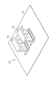
- FIG. 1 schematically shows an external appearance of a specific example of an electronic device, that is, a server computer device 11.
- the server computer device 11 includes a housing 12.
- a housing space is defined in the housing 12.
- a motherboard is disposed in the accommodation space.
- a semiconductor component such as an electronic component package and a main memory are mounted on the motherboard.
- the electronic component package executes various arithmetic processes based on, for example, software programs and data temporarily stored in the main memory.
- the software program and data may be stored in a large-capacity storage device such as a hard disk drive (HDD) that is similarly arranged in the accommodation space.
- HDD hard disk drive
- Such a server computer device 11 is mounted on a rack, for example.
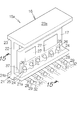
- FIG. 2 schematically shows the appearance of the printed circuit board unit according to the present invention, that is, the mother board 13.
- the motherboard 13 includes a large printed wiring board 14.
- a resin substrate is used for the printed wiring board 14.
- a surface mount type printed circuit board module 15 is mounted on the flat surface of the printed wiring board 14.
- the printed circuit board module 15 includes a mold 16 that stands upright from the surface of the printed wiring board 14.
- a printed circuit board 17 is held on the mold 16.
- the printed circuit board 17 establishes a vertical posture standing upright from the surface of the printed wiring board 14.
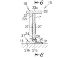
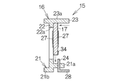
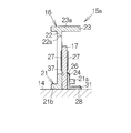
- FIG. 3 schematically shows the structure of the printed circuit board module 15 according to the first embodiment of the present invention.
- the mold 16 includes a pedestal 21 that spreads flat along the surface of the printed wiring board 14.
- the pedestal 21 is received on the surface of the object, that is, the printed wiring board 14 with a flat bottom surface. In this way, the base 21 is self-supporting on the surface of the printed wiring board 14.
- the mold 16 includes a side wall 22 that is integrated with the pedestal 21 based on integral molding.
- the side wall 22 is formed in a flat plate shape, for example.
- the side wall 22 stands vertically from the upper surface of the pedestal 21.
- the pedestal 21 defines a first pedestal 21 a on the front side of the side wall 22 and a second pedestal 21 b on the rear side of the side wall 22.
- the width of the first pedestal 21a defined in the second direction orthogonal to the first direction defined in the longitudinal direction of the pedestal 21 is set larger than the width of the second pedestal 21b defined in the second direction.
- the mold 16 includes a top plate 23 that is integrated with the upper end of the side wall 22 based on integral molding.
- the top plate 23 extends parallel to the pedestal 21.
- the top plate 23 is formed in a flat plate shape, for example.
- an upward flat surface 23a is defined with a predetermined spread. As will be described later, the flat surface 23a forms an adsorption surface.
- Such a mold 16 is integrally molded from an insulating resin material.
- a predetermined space is formed between the base 21 and the top plate 23.
- a printed circuit board 17 is fitted in this space. The back surface of the printed circuit board 17 is received by the side wall 22. Thus, the printed circuit board 17 establishes a vertical posture along the side wall 22.
- the mold 16 includes a plurality of conductive terminals 24 protruding from the surface of the first pedestal 21a on the front side of the surface of the printed circuit board 17, for example.
- the conductive terminals 24 are arranged in the first direction.
- Each conductive terminal 24 is individually electrically connected to a corresponding conductive pad 25 formed on the surface of the printed circuit board 17.
- Solder material 26 is used in establishing the electrical connection.
- Each conductive pad 25 is connected to a wiring pattern (not shown) formed on the front surface or the back surface of the printed circuit board 17, for example. Such a wiring pattern is connected to the electronic component chip 27 mounted on the front surface or the back surface of the printed circuit board 17.
- the mold 16 includes a plurality of surface mount terminals 28 protruding from the first pedestal 21 a along a virtual plane including the bottom surface of the pedestal 21.
- Each surface mount terminal 28 is electrically connected to a corresponding conductive pad 29 formed on the surface of the printed wiring board 14.
- Solder material 31 is used in establishing the electrical connection.
- a corresponding wiring pattern 32 formed on the surface of the printed wiring board 14 is connected to the conductive pad 29.
- the side wall 22 is formed from a frame, for example. Thus, a through hole 22 a is formed in the side wall 22.
- An electronic component chip 27 mounted on the back surface of the printed wiring board 14 is received in the through hole 22a.
- the conductive terminal 24 and the corresponding surface mount terminal 28 are integrated in the first pedestal 21a. That is, the conductive terminal 24 and the surface mount terminal 28 are partially embedded in the first pedestal 21a. In this way, other electronic components (not shown) on the printed wiring board 14 are connected to the electronic component chip 27 on the printed circuit board 17.
- the conductive terminal 24 extends along the surface of the first pedestal 21a.
- the conductive terminal 24 receives the lower end of the printed circuit board 17 based on elastic deformation. Based on the elastic force of the elastic terminal 24, the upper end of the printed circuit board 17 is pressed against the top plate 23. Thus, the printed circuit board 17 is fitted between the conductive terminals 24 and the top plate 23 in a vertical posture.
- the width of the mold 16 from the rear edge of the second pedestal 21 b to the front end of the surface mounting terminal 28 is set to about one half of the height from the surface of the printed wiring board 14 to the top plate 23. Is desirable.
- the mold 16, that is, the printed circuit board module 15 can stand on the surface of the printed wiring board 14.
- the first pedestal 21 a and the surface mount terminal 28 cooperate to constitute the first pedestal of the pedestal 21.
- the second pedestal 21 b constitutes the second pedestal of the pedestal 21.
- the independence of the pedestal 21, that is, the printed circuit board module 15 is established by the first leg and the second leg.
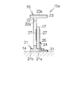
- a plurality of notches 33 are defined at the lower end of the printed circuit board 17.
- the notch 33 defines the outline of the printed circuit board 17.
- each notch 33 defines a semi-cylindrical space, for example.
- Each notch 33 receives a corresponding conductive terminal 24.
- the displacement of the printed circuit board 17 is regulated in the first direction by the action of the notches 33.
- the printed circuit board 17 is sandwiched between the conductive terminals 24 and the top plate 23. As a result, the printed board 17 is prevented from dropping from the mold 16.
- the above-described conductive pad 25 is formed around each notch 33.
- the printed circuit board module 15 is assembled. As shown in FIG. 7, in the mold 16, the conductive terminals 24 extend in parallel to the surface of the first pedestal 21a. The lower end of the inclined printed circuit board 17 is abutted against the conductive terminal 24. The conductive terminal 24 is received in the notch 33. Thus, the printed circuit board 17 is accurately positioned with respect to the mold 16. The conductive terminal 24 is elastically deformed. The printed circuit board 17 rotates from the inclined posture toward the vertical posture with the conductive terminal 24 as a fulcrum. Thus, the back surface of the printed circuit board 17 is received by the side wall 22. At the same time, the upper end of the printed circuit board 17 is received by the top plate 23. The printed circuit board 17 is fitted between the conductive terminal 24 and the top plate 23 based on the elastic deformation of the conductive terminal 24.
- the solder paste 34 may be applied in advance on the conductive pads 25 of the printed circuit board 17.
- the printed circuit board module 15 thus assembled is transported onto the printed wiring board 14.
- an automatic mounting robot 35 is attracted to the flat surface 23 a of the top plate 23.
- a solder paste (not shown) is previously applied on the conductive pads 29 on the printed wiring board 14.
- the surface mount terminals 28 are received by the solder paste on the conductive pads 29.
- the printed circuit board module 15 can stand by the function of the base 21. In this state, a reflow process is performed on the printed wiring board 14.
- the solder of the solder paste on the conductive pads 25 and 29 melts. Thereafter, the solder solidifies based on the cooling.
- the printed circuit board module 15 is mounted on the printed wiring board 14.
- the printed circuit board module 15 since the pedestal 21, the side wall 22 and the top plate 23 are integrated based on integral molding, the printed circuit board module 15 is simply configured.
- the conductive terminal 24 is used for fitting the printed circuit board 17.
- the printed circuit board 17 is securely held between the conductive terminal 24 and the top plate 23 based on the elastic force of the conductive terminal 24.
- the printed circuit board 17 is easily positioned with respect to the mold 16 by the action of the notches 33.
- the printed circuit board module 15 can stand on the printed wiring board 14 by the function of the base 21.
- the printed circuit board 17 establishes a vertical posture.
- the mounting area is reduced on the printed wiring board 14. Mounting density is improved.
- the solder paste is applied onto the conductive pads 25 and 29, the mounting of the printed circuit board module 15 is completed in a single reflow process. The manufacturing process is simplified.
- the top plate 23 can be used for suction of the automatic mounting robot 35.
- FIG. 9 schematically shows the structure of a printed circuit board module 15a according to the second embodiment of the present invention.
- the first pedestal 21 a is disposed at a predetermined height from the surface of the printed wiring board 14.
- the first pedestal 21a and the second pedestal 21b are arranged at different levels.
- the printed circuit board 17 is fitted in a vertical posture in a space formed between the first pedestal 21 a and the top plate 23.
- a pair of guide walls 36, 36 are integrated with the side wall 22.
- the guide walls 36, 36 protrude from the surface of the side wall 22.
- the printed circuit board 17 is accommodated between the guide walls 36 and 36.
- the printed circuit board 17 is easily positioned in the first direction by the action of the guide walls 36.
- the conductive terminal 24 protruding from the surface of the first base 21 a is pressed against the conductive pad 29 on the surface of the printed circuit board 17.
- the conductive pad 29 is formed along the contour of the lower end of the printed circuit board 17.
- the printed circuit board 17 is pressed toward the side wall 22 based on the elastic force of the conductive terminal 24.
- the surface mounting terminal 28 protrudes from the back surface of the first pedestal 21a and extends along the above-described virtual plane based on the bending.
- the surface mount terminal 28 forms the second foot of the base 21 as described above.
- Like reference numerals are attached to the structure or components equivalent to those of the aforementioned printed circuit board module 15. According to such a printed circuit board module 15a, the same effects as described above are realized.
- the printed circuit board 17 is pressed toward the side wall 22 above the upper end of the conductive terminal 24, as shown in FIG. At this time, the printed circuit board 17 is easily positioned with respect to the mold 16 in the first direction by the action of the guide walls 36 and 36. Thereafter, the printed circuit board 17 is pushed down toward the base 21 based on the guidance of the guide walls 36 and 36. As a result, the printed circuit board 17 is fitted between the conductive terminal 24 and the side wall 22 in a vertical posture. The conductive terminals 24 are positioned on corresponding conductive pads 25 on the printed circuit board 17. Then, the reflow process should just be implemented similarly to the above-mentioned.
- the first pedestal 21a may be arranged at the same height as the second pedestal 21b. In this way, the first pedestal 21 a is received on the surface of the printed wiring board 14 in the same manner as the printed circuit board module 15 described above. Referring also to FIG. 13, the surface mount terminal 28 protrudes from the front end of the first base 21 a along the above-described virtual plane. Like reference numerals are attached to the structure or components equivalent to those of the aforementioned printed circuit board module 15. According to such a printed circuit board module 15a, the same effects as described above are realized.
- a through hole 37 penetrating from the front surface to the back surface may be formed in the first pedestal 21a.
- the through hole 37 receives the printed circuit board 17.
- the formation of the guide walls 36, 36 may be omitted from the side wall 22.
- the first pedestal 21 a is disposed at a predetermined height from the surface of the printed wiring board 14.
- the printed circuit board 17 is positioned in the first direction by the action of the through hole 37.
- Like reference numerals are attached to the structure or components equivalent to those of the aforementioned printed circuit board module 15. According to such a printed circuit board module 15a, the same effects as described above are realized.
- FIG. 16 schematically shows the structure of a printed circuit board module 15b according to the third embodiment of the present invention.
- This printed circuit board module 15 b includes a mold 41.
- the mold 41 includes a pedestal 42.
- the pedestal 42 is received on the surface of the printed wiring board 14 with a flat bottom surface.
- the pedestal 42 has a first foot 42a.
- the side wall 22 is integrated with the pedestal 42 based on integral molding.
- a top plate 23 is integrated with the side wall 22 based on integral molding.
- Such a mold 41 is integrally molded from an insulating resin material.
- a printed circuit board 17 is held on the side wall 22.
- the printed circuit board 17 extends from the top plate 23 toward the base 42.
- a plurality of conductive terminals 24 extend in parallel along the surface of the printed circuit board 17.
- the conductive terminal 24 is fixed to the conductive pad 25 on the printed circuit board 17 by the solder material 26 described above. All the conductive terminals 24 are connected by a holding mold 43.
- the holding mold 43 is formed from an insulating resin material.
- a corresponding surface mount terminal 28 is integrated with each conductive terminal 24.
- the surface mounting terminal 28 extends along a virtual plane including the bottom surface of the base 42.
- the surface mounting terminals 28 are connected to the conductive pads 29 on the printed wiring board 14.
- the surface mount terminal 28 constitutes a second foot.
- the surface mount terminal 28 establishes self-support of the pedestal 42, that is, the printed circuit board module 15b, in cooperation with the first foot 42a.
- the protrusion 44 protrudes from the surface of the side wall 22.
- the protrusions 44 are arranged at the four corners on the surface of the side wall 22.
- the protrusion 44 is received in the through hole 45 that penetrates the printed circuit board 17 from the front surface to the back surface.
- the protrusion 44 includes a pair of shaft members 46 that face each other on an inward surface.
- the shaft member 46 can be elastically deformed.
- a locking piece 46 a that engages with the surface of the printed circuit board 17 is defined at the tip of the shaft member 46. Due to the action of the locking piece 46a, the printed board 17 is prevented from falling off from the protrusion 44.
- the printed circuit board 17 is held on the side wall 22, that is, the mold 41.
- the conductive terminals 24 are soldered to the surface of the printed circuit board 17.
- the conductive terminal 24 is held by the holding mold 43.
- the printed circuit board 17 is attached to the mold 41.
- the through hole 45 is positioned on the protrusion 44. As shown in FIG. 19, when the locking piece 46 a is pressed against the opening of the through hole 45, the locking pieces 46 a come closer to each other based on the elastic deformation of the shaft member 46. As a result, the locking piece 46 a is received in the through hole 45.
- the locking piece 46 a comes out of the through hole 45, the locking piece 46 a is received on the surface of the printed circuit board 17 based on the elastic restoring force of the shaft member 46. In this way, the printed circuit board 17 is held by the mold 41. Thus, the printed circuit board module 15b is assembled.
- the printed circuit board module 15b since the pedestal 42, the side wall 22 and the top plate 23 are integrated based on integral molding, the printed circuit board module 15b is simply configured. Moreover, the protrusions 44 are used for fitting the printed circuit board 17. The printed circuit board 17 is easily positioned with respect to the mold 41 by the action of the protrusions 44. Further, the printed circuit board module 15 b can stand on the printed wiring board 14 by the action of the base 42 and the surface mounting terminals 28. Mounting density is improved. In addition, the top plate 23 is used for suction of the automatic mounting robot 35 as described above.
- the mold 41 may be formed of, for example, a metal material.
- the metal material include aluminum and copper.
- the printed circuit board 17 is received by the side wall 22.
- the electronic component chip 27 generates heat energy based on heat generation. Thermal energy is transmitted to the side wall 22, that is, the mold 41 through the printed circuit board 17. Thermal energy is radiated from the mold 41 having a relatively large surface area to the atmosphere. Thus, an excessive temperature rise of the electronic component chip 27 is prevented.
Landscapes
- Engineering & Computer Science (AREA)
- Microelectronics & Electronic Packaging (AREA)
- Manufacturing & Machinery (AREA)
- Combinations Of Printed Boards (AREA)
- Casings For Electric Apparatus (AREA)
Abstract
Description
図3は本発明の第1実施形態に係るプリント基板モジュール15の構造を概略的に示す。このプリント基板モジュール15では、モールド16は、プリント配線板14の表面に沿って平たく広がる台座21を備える。台座21は、平坦な底面で対象物すなわちプリント配線板14の表面に受け止められる。こうして台座21はプリント配線板14の表面で自立する。モールド16は、一体成型に基づき台座21に一体化される側壁22を備える。側壁22は例えば平たい板状に形成される。側壁22は台座21の上面から垂直に立つ。台座21は、側壁22より前側の第1台座21aと、側壁22より後側の第2台座21bとを区画する。ここでは、台座21の長手方向に規定される第1方向に直交する第2方向に規定される第1台座21aの幅は、第2方向に規定される第2台座21bの幅より大きく設定される。
Claims (13)
- 樹脂製の台座と、
前記台座から垂直に立ち、一体成型に基づき前記台座に一体化される樹脂製の側壁と、
所定の広がりで上向きの平坦面を規定し、前記台座との間に所定の空間を形成しつつ一体成型に基づき前記側壁に一体化される樹脂製の天板と、
前記台座の表面から突き出る弾性の導電端子と、
前記所定の空間に収容され、前記導電端子の弾性力に基づき前記導電端子および前記天板の間に垂直姿勢ではめ込まれるプリント基板とを備えることを特徴とするプリント基板モジュール。 - 請求項1に記載のプリント基板モジュールにおいて、
前記プリント基板の輪郭を規定し、前記導電端子を受け入れる切り欠きと、
前記切り欠き周りで前記プリント基板の表面に形成される導電パッドとを備えることを特徴とするプリント基板モジュール。 - 請求項1または2に記載のプリント基板モジュールにおいて、
前記台座に形成されて対象物に受け止められる平坦な底面と、
前記底面を含む仮想平面に沿って前記台座から突き出て、前記導電端子に一体化される表面実装端子とを備えることを特徴とするプリント基板モジュール。 - プリント配線板と、平坦な底面で前記プリント配線板の表面に受け止められる樹脂製の台座と、前記台座から垂直に立ち、一体成型に基づき前記台座に一体化される樹脂製の側壁と、所定の広がりで上向きの平坦面を規定し、前記台座との間に所定の空間を形成しつつ一体成型に基づき前記側壁に一体化される樹脂製の天板と、前記台座の表面から突き出る弾性の導電端子と、前記所定の空間に収容され、前記導電端子の弾性力に基づき前記導電端子および前記天板の間に垂直姿勢ではめ込まれるプリント基板とを備えることを特徴とするプリント基板ユニット。
- 樹脂製の台座と、
前記台座から垂直に立ち、一体成型に基づき前記台座に一体化される樹脂製の側壁と、
所定の広がりで上向きの平坦面を規定し、前記台座との間に所定の空間を形成しつつ一体成型に基づき前記側壁に一体化される樹脂製の天板と、
前記台座の表面から突き出る弾性の導電端子と、
前記所定の空間に収容され、前記導電端子の弾性力に基づき前記導電端子および前記側壁の間に垂直姿勢ではめ込まれるプリント基板とを備えることを特徴とするプリント基板モジュール。 - 請求項5に記載のプリント基板モジュールにおいて、前記台座から突き出て前記台座の台足を構成し、前記導電端子に一体化される表面実装端子を備えることを特徴とするプリント基板モジュール。
- 請求項5に記載のプリント基板モジュールにおいて、
前記台座に形成されて対象物に受け止められる底面と、
前記底面を含む仮想平面に沿って前記台座から突き出て、前記導電端子に一体化される表面実装端子とを備えることを特徴とするプリント基板モジュール。 - プリント配線板と、平坦な底面で前記プリント配線板の表面に受け止められる樹脂製の台座と、前記台座から垂直に立ち、一体成型に基づき前記台座に一体化される樹脂製の側壁と、所定の広がりで上向きの平坦面を規定し、前記台座との間に所定の空間を形成しつつ一体成型に基づき前記側壁に一体化される樹脂製の天板と、前記台座の表面から突き出る弾性の導電端子と、前記所定の空間に収容され、前記導電端子の弾性力に基づき前記導電端子および前記側壁の間に垂直姿勢ではめ込まれるプリント基板とを備えることを特徴とするプリント基板ユニット。
- 第1台足を有する台座と、
前記台座から垂直に立ち、一体成型に基づき前記台座に一体化される側壁と、
所定の広がりで上向きの平坦面を規定し、一体成型に基づき前記側壁に一体化される天板と、
前記天板から前記台座に向かって広がりつつ前記側壁に保持されるプリント基板と、
前記プリント基板の表面に固定されて、前記第1台足と協働で前記台座の自立を確立する第2台足とを備えることを特徴とするプリント基板モジュール。 - 請求項9に記載のプリント基板モジュールにおいて、前記第2台足を構成する表面実装端子を備えることを特徴とするプリント基板モジュール。
- 請求項9または10に記載のプリント基板モジュールにおいて、前記台座、前記側壁および前記天板は樹脂材料から形成されることを特徴とするプリント基板モジュール。
- 請求項9または10に記載のプリント基板モジュールにおいて、前記台座、前記側壁および前記天板は金属材料から形成されることを特徴とするプリント基板モジュール。
- プリント配線板と、平坦な底面で前記プリント配線板の表面に受け止められ、第1台足を有する台座と、前記台座から垂直に立ち、一体成型に基づき前記台座に一体化される側壁と、所定の広がりで上向きの平坦面を規定し、一体成型に基づき前記側壁に一体化される天板と、前記天板から前記台座に向かって広がりつつ前記側壁に保持されるプリント基板と、前記プリント基板の表面に固定されて、前記第1台足と協働で前記台座の自立を確立する第2台足とを備えることを特徴とするプリント基板ユニット。
Priority Applications (6)
| Application Number | Priority Date | Filing Date | Title |
|---|---|---|---|
| CN200980157541.2A CN102334390B (zh) | 2009-03-04 | 2009-03-04 | 印刷基板模块 |
| KR1020117019714A KR101178827B1 (ko) | 2009-03-04 | 2009-03-04 | 프린트 기판 모듈 |
| JP2011502532A JP5120492B2 (ja) | 2009-03-04 | 2009-03-04 | プリント基板モジュール |
| PCT/JP2009/054049 WO2010100726A1 (ja) | 2009-03-04 | 2009-03-04 | プリント基板モジュール |
| EP09841091.3A EP2405724B1 (en) | 2009-03-04 | 2009-03-04 | Printed circuit board module |
| US13/218,017 US8455767B2 (en) | 2009-03-04 | 2011-08-25 | Printed circuit board module |
Applications Claiming Priority (1)
| Application Number | Priority Date | Filing Date | Title |
|---|---|---|---|
| PCT/JP2009/054049 WO2010100726A1 (ja) | 2009-03-04 | 2009-03-04 | プリント基板モジュール |
Related Child Applications (1)
| Application Number | Title | Priority Date | Filing Date |
|---|---|---|---|
| US13/218,017 Continuation US8455767B2 (en) | 2009-03-04 | 2011-08-25 | Printed circuit board module |
Publications (1)
| Publication Number | Publication Date |
|---|---|
| WO2010100726A1 true WO2010100726A1 (ja) | 2010-09-10 |
Family
ID=42709304
Family Applications (1)
| Application Number | Title | Priority Date | Filing Date |
|---|---|---|---|
| PCT/JP2009/054049 WO2010100726A1 (ja) | 2009-03-04 | 2009-03-04 | プリント基板モジュール |
Country Status (6)
| Country | Link |
|---|---|
| US (1) | US8455767B2 (ja) |
| EP (1) | EP2405724B1 (ja) |
| JP (1) | JP5120492B2 (ja) |
| KR (1) | KR101178827B1 (ja) |
| CN (1) | CN102334390B (ja) |
| WO (1) | WO2010100726A1 (ja) |
Cited By (1)
| Publication number | Priority date | Publication date | Assignee | Title |
|---|---|---|---|---|
| US20120099288A1 (en) * | 2010-10-22 | 2012-04-26 | Murata Power Solutions (Milton Keynes) Limited | Electronic component for surface mounting |
Families Citing this family (4)
| Publication number | Priority date | Publication date | Assignee | Title |
|---|---|---|---|---|
| DE102013207384A1 (de) * | 2013-04-24 | 2014-10-30 | Robert Bosch Gmbh | Schaltungsträger, Anordnung mit einem Schaltungsträger und Verfahren zum Herstellen einer elektrischen Kontaktierung |
| US10681821B2 (en) * | 2014-10-16 | 2020-06-09 | The Charles Stark Draper Laboratory, Inc. | Methods and devices for improved space utilization in wafer based modules |
| US10820428B2 (en) * | 2017-06-28 | 2020-10-27 | The Boeing Company | Attachment apparatus and methods for use |
| JP7088409B2 (ja) * | 2019-04-03 | 2022-06-21 | 株式会社村田製作所 | モジュール、端子集合体、及びモジュールの製造方法 |
Citations (9)
| Publication number | Priority date | Publication date | Assignee | Title |
|---|---|---|---|---|
| JPH0459971U (ja) * | 1990-09-29 | 1992-05-22 | ||
| JPH0528067U (ja) * | 1991-09-21 | 1993-04-09 | 太陽誘電株式会社 | 面実装用混成集積回路装置 |
| JPH0617269U (ja) * | 1992-07-31 | 1994-03-04 | ミツミ電機株式会社 | 立ち基板ホルダー |
| JP2000208819A (ja) * | 1999-01-14 | 2000-07-28 | Rohm Co Ltd | 発光ダイオ―ド表示器 |
| JP2004153178A (ja) | 2002-10-31 | 2004-05-27 | Matsushita Electric Works Ltd | 複数のプリント基板を有する電子装置 |
| US6815614B1 (en) | 2003-09-05 | 2004-11-09 | Power-One Limited | Arrangement for co-planar vertical surface mounting of subassemblies on a mother board |
| JP2005150498A (ja) * | 2003-11-18 | 2005-06-09 | Funai Electric Co Ltd | 立ち基板付き配線基板 |
| JP2006024746A (ja) | 2004-07-08 | 2006-01-26 | Matsushita Electric Ind Co Ltd | 電子回路装置 |
| JP2006173152A (ja) | 2004-12-13 | 2006-06-29 | Matsushita Electric Ind Co Ltd | 中継基板と立体配線構造体 |
Family Cites Families (10)
| Publication number | Priority date | Publication date | Assignee | Title |
|---|---|---|---|---|
| US4089042A (en) * | 1976-11-22 | 1978-05-09 | Gte Automatic Electric Laboratories Incorporated | Support for hybrid substrate carrying electrical circuit patterns and elements |
| DE3146608A1 (de) * | 1981-11-25 | 1983-07-07 | Robert Bosch Gmbh, 7000 Stuttgart | Anordnung aus einer leiterplatte, einer hybridplatte und einem halter |
| JP2637265B2 (ja) | 1990-06-28 | 1997-08-06 | 株式会社東芝 | 窒化珪素膜の形成方法 |
| JPH0528067A (ja) | 1991-07-19 | 1993-02-05 | Nec Corp | コンピユータシステム |
| JPH0617269A (ja) | 1992-07-03 | 1994-01-25 | Kawasaki Steel Corp | ステンレス冷延鋼板の製造方法 |
| AU2003266642A1 (en) | 2002-10-28 | 2004-05-13 | Matsushita Electric Works, Ltd. | High-pressure discharge lamp operation device and illumination appliance having the same |
| DE10337443A1 (de) * | 2003-08-14 | 2005-03-24 | Siemens Ag | Schaltungsanordnung insbesondere für ein Kraftfahrzeug- Insassenschutzsystem |
| US7613010B2 (en) * | 2004-02-02 | 2009-11-03 | Panasonic Corporation | Stereoscopic electronic circuit device, and relay board and relay frame used therein |
| US7845954B2 (en) * | 2005-07-14 | 2010-12-07 | Panasonic Corporation | Interconnecting board and three-dimensional wiring structure using it |
| CN101997187B (zh) * | 2009-08-21 | 2014-04-23 | 鸿富锦精密工业(深圳)有限公司 | 微机电系统插头及插座连接器、其制作方法及连接器组合 |
-
2009
- 2009-03-04 WO PCT/JP2009/054049 patent/WO2010100726A1/ja active Application Filing
- 2009-03-04 KR KR1020117019714A patent/KR101178827B1/ko not_active IP Right Cessation
- 2009-03-04 CN CN200980157541.2A patent/CN102334390B/zh not_active Expired - Fee Related
- 2009-03-04 EP EP09841091.3A patent/EP2405724B1/en not_active Not-in-force
- 2009-03-04 JP JP2011502532A patent/JP5120492B2/ja not_active Expired - Fee Related
-
2011
- 2011-08-25 US US13/218,017 patent/US8455767B2/en not_active Expired - Fee Related
Patent Citations (9)
| Publication number | Priority date | Publication date | Assignee | Title |
|---|---|---|---|---|
| JPH0459971U (ja) * | 1990-09-29 | 1992-05-22 | ||
| JPH0528067U (ja) * | 1991-09-21 | 1993-04-09 | 太陽誘電株式会社 | 面実装用混成集積回路装置 |
| JPH0617269U (ja) * | 1992-07-31 | 1994-03-04 | ミツミ電機株式会社 | 立ち基板ホルダー |
| JP2000208819A (ja) * | 1999-01-14 | 2000-07-28 | Rohm Co Ltd | 発光ダイオ―ド表示器 |
| JP2004153178A (ja) | 2002-10-31 | 2004-05-27 | Matsushita Electric Works Ltd | 複数のプリント基板を有する電子装置 |
| US6815614B1 (en) | 2003-09-05 | 2004-11-09 | Power-One Limited | Arrangement for co-planar vertical surface mounting of subassemblies on a mother board |
| JP2005150498A (ja) * | 2003-11-18 | 2005-06-09 | Funai Electric Co Ltd | 立ち基板付き配線基板 |
| JP2006024746A (ja) | 2004-07-08 | 2006-01-26 | Matsushita Electric Ind Co Ltd | 電子回路装置 |
| JP2006173152A (ja) | 2004-12-13 | 2006-06-29 | Matsushita Electric Ind Co Ltd | 中継基板と立体配線構造体 |
Non-Patent Citations (1)
| Title |
|---|
| See also references of EP2405724A4 |
Cited By (3)
| Publication number | Priority date | Publication date | Assignee | Title |
|---|---|---|---|---|
| US20120099288A1 (en) * | 2010-10-22 | 2012-04-26 | Murata Power Solutions (Milton Keynes) Limited | Electronic component for surface mounting |
| CN102457177A (zh) * | 2010-10-22 | 2012-05-16 | 村田电源技术(米尔顿凯恩斯)有限公司 | 用于表面安装的电子部件 |
| US8923010B2 (en) * | 2010-10-22 | 2014-12-30 | Murata Power Solutions (Milton Keynes) Limited | Electronic component for surface mounting |
Also Published As
| Publication number | Publication date |
|---|---|
| US8455767B2 (en) | 2013-06-04 |
| EP2405724A1 (en) | 2012-01-11 |
| EP2405724A4 (en) | 2013-04-03 |
| CN102334390A (zh) | 2012-01-25 |
| EP2405724B1 (en) | 2014-06-04 |
| KR101178827B1 (ko) | 2012-09-03 |
| KR20110119750A (ko) | 2011-11-02 |
| US20110308839A1 (en) | 2011-12-22 |
| JPWO2010100726A1 (ja) | 2012-09-06 |
| CN102334390B (zh) | 2014-01-22 |
| JP5120492B2 (ja) | 2013-01-16 |
Similar Documents
| Publication | Publication Date | Title |
|---|---|---|
| JP5120492B2 (ja) | プリント基板モジュール | |
| JP4985779B2 (ja) | プリント基板ユニットおよびソケット | |
| JP2006279485A (ja) | 高安定圧電発振器 | |
| US9942988B2 (en) | Circuit board and power supply apparatus | |
| US20090129024A1 (en) | Inverted through circuit board mounting with heat sink | |
| JP2001143840A (ja) | 電子部品用ソケット | |
| US9004959B2 (en) | Electrical connecting device | |
| US7320602B2 (en) | Substrate structure, substrate manufacturing method and electronic device | |
| JP2008213926A (ja) | テーピング部品 | |
| JP2009193677A (ja) | アダプタ、ソケット、電子装置および実装方法 | |
| KR100829100B1 (ko) | 부품실장 회로기판 및 이를 가지는 전자장치 | |
| JP2004207565A (ja) | 基板接続構造及びそれを用いた電源装置 | |
| JP6447401B2 (ja) | コネクタ実装基板 | |
| JP2008166525A (ja) | 電子回路モジュール | |
| JP2011034914A (ja) | コンタクト及びそれを備えるソケット | |
| US20050026478A1 (en) | Solder bearing conductive terminal | |
| JP2003187890A (ja) | 電気接続端子 | |
| JP2008016419A (ja) | ソケット | |
| JPH0353477Y2 (ja) | ||
| JPH05327161A (ja) | 電子回路モジュール | |
| JPS635248Y2 (ja) | ||
| US6648655B1 (en) | Land grid array socket with supporting members | |
| JP2013219234A (ja) | 回路基板 | |
| JP5618140B2 (ja) | 回路構成体および電気接続箱 | |
| JPH11121117A (ja) | コネクタ付きモジュール及びその製造方法 |
Legal Events
| Date | Code | Title | Description |
|---|---|---|---|
| WWE | Wipo information: entry into national phase |
Ref document number: 200980157541.2 Country of ref document: CN |
|
| 121 | Ep: the epo has been informed by wipo that ep was designated in this application |
Ref document number: 09841091 Country of ref document: EP Kind code of ref document: A1 |
|
| WWE | Wipo information: entry into national phase |
Ref document number: 2011502532 Country of ref document: JP |
|
| ENP | Entry into the national phase |
Ref document number: 20117019714 Country of ref document: KR Kind code of ref document: A |
|
| WWE | Wipo information: entry into national phase |
Ref document number: 2009841091 Country of ref document: EP |
|
| NENP | Non-entry into the national phase |
Ref country code: DE |