WO2010098500A1 - 半導体装置及びその製造方法 - Google Patents
半導体装置及びその製造方法 Download PDFInfo
- Publication number
- WO2010098500A1 WO2010098500A1 PCT/JP2010/053487 JP2010053487W WO2010098500A1 WO 2010098500 A1 WO2010098500 A1 WO 2010098500A1 JP 2010053487 W JP2010053487 W JP 2010053487W WO 2010098500 A1 WO2010098500 A1 WO 2010098500A1
- Authority
- WO
- WIPO (PCT)
- Prior art keywords
- island
- lead
- resin package
- wire
- semiconductor device
- Prior art date
- Legal status (The legal status is an assumption and is not a legal conclusion. Google has not performed a legal analysis and makes no representation as to the accuracy of the status listed.)
- Ceased
Links
Images




Classifications
-
- H—ELECTRICITY
- H10—SEMICONDUCTOR DEVICES; ELECTRIC SOLID-STATE DEVICES NOT OTHERWISE PROVIDED FOR
- H10W—GENERIC PACKAGES, INTERCONNECTIONS, CONNECTORS OR OTHER CONSTRUCTIONAL DETAILS OF DEVICES COVERED BY CLASS H10
- H10W70/00—Package substrates; Interposers; Redistribution layers [RDL]
- H10W70/40—Leadframes
- H10W70/411—Chip-supporting parts, e.g. die pads
-
- H—ELECTRICITY
- H10—SEMICONDUCTOR DEVICES; ELECTRIC SOLID-STATE DEVICES NOT OTHERWISE PROVIDED FOR
- H10W—GENERIC PACKAGES, INTERCONNECTIONS, CONNECTORS OR OTHER CONSTRUCTIONAL DETAILS OF DEVICES COVERED BY CLASS H10
- H10W72/00—Interconnections or connectors in packages
- H10W72/01—Manufacture or treatment
- H10W72/019—Manufacture or treatment of bond pads
-
- H—ELECTRICITY
- H10—SEMICONDUCTOR DEVICES; ELECTRIC SOLID-STATE DEVICES NOT OTHERWISE PROVIDED FOR
- H10W—GENERIC PACKAGES, INTERCONNECTIONS, CONNECTORS OR OTHER CONSTRUCTIONAL DETAILS OF DEVICES COVERED BY CLASS H10
- H10W72/00—Interconnections or connectors in packages
- H10W72/01—Manufacture or treatment
- H10W72/015—Manufacture or treatment of bond wires
- H10W72/01551—Changing the shapes of bond wires
-
- H—ELECTRICITY
- H10—SEMICONDUCTOR DEVICES; ELECTRIC SOLID-STATE DEVICES NOT OTHERWISE PROVIDED FOR
- H10W—GENERIC PACKAGES, INTERCONNECTIONS, CONNECTORS OR OTHER CONSTRUCTIONAL DETAILS OF DEVICES COVERED BY CLASS H10
- H10W72/00—Interconnections or connectors in packages
- H10W72/01—Manufacture or treatment
- H10W72/0198—Manufacture or treatment batch processes
-
- H—ELECTRICITY
- H10—SEMICONDUCTOR DEVICES; ELECTRIC SOLID-STATE DEVICES NOT OTHERWISE PROVIDED FOR
- H10W—GENERIC PACKAGES, INTERCONNECTIONS, CONNECTORS OR OTHER CONSTRUCTIONAL DETAILS OF DEVICES COVERED BY CLASS H10
- H10W72/00—Interconnections or connectors in packages
- H10W72/071—Connecting or disconnecting
- H10W72/0711—Apparatus therefor
- H10W72/07141—Means for applying energy, e.g. ovens or lasers
-
- H—ELECTRICITY
- H10—SEMICONDUCTOR DEVICES; ELECTRIC SOLID-STATE DEVICES NOT OTHERWISE PROVIDED FOR
- H10W—GENERIC PACKAGES, INTERCONNECTIONS, CONNECTORS OR OTHER CONSTRUCTIONAL DETAILS OF DEVICES COVERED BY CLASS H10
- H10W72/00—Interconnections or connectors in packages
- H10W72/071—Connecting or disconnecting
- H10W72/0711—Apparatus therefor
- H10W72/07178—Means for aligning
-
- H—ELECTRICITY
- H10—SEMICONDUCTOR DEVICES; ELECTRIC SOLID-STATE DEVICES NOT OTHERWISE PROVIDED FOR
- H10W—GENERIC PACKAGES, INTERCONNECTIONS, CONNECTORS OR OTHER CONSTRUCTIONAL DETAILS OF DEVICES COVERED BY CLASS H10
- H10W72/00—Interconnections or connectors in packages
- H10W72/071—Connecting or disconnecting
- H10W72/073—Connecting or disconnecting of die-attach connectors
-
- H—ELECTRICITY
- H10—SEMICONDUCTOR DEVICES; ELECTRIC SOLID-STATE DEVICES NOT OTHERWISE PROVIDED FOR
- H10W—GENERIC PACKAGES, INTERCONNECTIONS, CONNECTORS OR OTHER CONSTRUCTIONAL DETAILS OF DEVICES COVERED BY CLASS H10
- H10W72/00—Interconnections or connectors in packages
- H10W72/071—Connecting or disconnecting
- H10W72/075—Connecting or disconnecting of bond wires
- H10W72/07502—Connecting or disconnecting of bond wires using an auxiliary member
-
- H—ELECTRICITY
- H10—SEMICONDUCTOR DEVICES; ELECTRIC SOLID-STATE DEVICES NOT OTHERWISE PROVIDED FOR
- H10W—GENERIC PACKAGES, INTERCONNECTIONS, CONNECTORS OR OTHER CONSTRUCTIONAL DETAILS OF DEVICES COVERED BY CLASS H10
- H10W72/00—Interconnections or connectors in packages
- H10W72/071—Connecting or disconnecting
- H10W72/075—Connecting or disconnecting of bond wires
- H10W72/07511—Treating the bonding area before connecting, e.g. by applying flux or cleaning
-
- H—ELECTRICITY
- H10—SEMICONDUCTOR DEVICES; ELECTRIC SOLID-STATE DEVICES NOT OTHERWISE PROVIDED FOR
- H10W—GENERIC PACKAGES, INTERCONNECTIONS, CONNECTORS OR OTHER CONSTRUCTIONAL DETAILS OF DEVICES COVERED BY CLASS H10
- H10W72/00—Interconnections or connectors in packages
- H10W72/071—Connecting or disconnecting
- H10W72/075—Connecting or disconnecting of bond wires
- H10W72/07521—Aligning
-
- H—ELECTRICITY
- H10—SEMICONDUCTOR DEVICES; ELECTRIC SOLID-STATE DEVICES NOT OTHERWISE PROVIDED FOR
- H10W—GENERIC PACKAGES, INTERCONNECTIONS, CONNECTORS OR OTHER CONSTRUCTIONAL DETAILS OF DEVICES COVERED BY CLASS H10
- H10W72/00—Interconnections or connectors in packages
- H10W72/071—Connecting or disconnecting
- H10W72/075—Connecting or disconnecting of bond wires
- H10W72/07531—Techniques
- H10W72/07532—Compression bonding, e.g. thermocompression bonding
- H10W72/07533—Ultrasonic bonding, e.g. thermosonic bonding
-
- H—ELECTRICITY
- H10—SEMICONDUCTOR DEVICES; ELECTRIC SOLID-STATE DEVICES NOT OTHERWISE PROVIDED FOR
- H10W—GENERIC PACKAGES, INTERCONNECTIONS, CONNECTORS OR OTHER CONSTRUCTIONAL DETAILS OF DEVICES COVERED BY CLASS H10
- H10W72/00—Interconnections or connectors in packages
- H10W72/071—Connecting or disconnecting
- H10W72/075—Connecting or disconnecting of bond wires
- H10W72/07541—Controlling the environment, e.g. atmosphere composition or temperature
-
- H—ELECTRICITY
- H10—SEMICONDUCTOR DEVICES; ELECTRIC SOLID-STATE DEVICES NOT OTHERWISE PROVIDED FOR
- H10W—GENERIC PACKAGES, INTERCONNECTIONS, CONNECTORS OR OTHER CONSTRUCTIONAL DETAILS OF DEVICES COVERED BY CLASS H10
- H10W72/00—Interconnections or connectors in packages
- H10W72/071—Connecting or disconnecting
- H10W72/075—Connecting or disconnecting of bond wires
- H10W72/07551—Connecting or disconnecting of bond wires characterised by changes in properties of the bond wires during the connecting
- H10W72/07553—Connecting or disconnecting of bond wires characterised by changes in properties of the bond wires during the connecting changes in shapes
-
- H—ELECTRICITY
- H10—SEMICONDUCTOR DEVICES; ELECTRIC SOLID-STATE DEVICES NOT OTHERWISE PROVIDED FOR
- H10W—GENERIC PACKAGES, INTERCONNECTIONS, CONNECTORS OR OTHER CONSTRUCTIONAL DETAILS OF DEVICES COVERED BY CLASS H10
- H10W72/00—Interconnections or connectors in packages
- H10W72/30—Die-attach connectors
- H10W72/321—Structures or relative sizes of die-attach connectors
- H10W72/325—Die-attach connectors having a filler embedded in a matrix
-
- H—ELECTRICITY
- H10—SEMICONDUCTOR DEVICES; ELECTRIC SOLID-STATE DEVICES NOT OTHERWISE PROVIDED FOR
- H10W—GENERIC PACKAGES, INTERCONNECTIONS, CONNECTORS OR OTHER CONSTRUCTIONAL DETAILS OF DEVICES COVERED BY CLASS H10
- H10W72/00—Interconnections or connectors in packages
- H10W72/30—Die-attach connectors
- H10W72/351—Materials of die-attach connectors
- H10W72/352—Materials of die-attach connectors comprising metals or metalloids, e.g. solders
-
- H—ELECTRICITY
- H10—SEMICONDUCTOR DEVICES; ELECTRIC SOLID-STATE DEVICES NOT OTHERWISE PROVIDED FOR
- H10W—GENERIC PACKAGES, INTERCONNECTIONS, CONNECTORS OR OTHER CONSTRUCTIONAL DETAILS OF DEVICES COVERED BY CLASS H10
- H10W72/00—Interconnections or connectors in packages
- H10W72/50—Bond wires
- H10W72/531—Shapes of wire connectors
- H10W72/536—Shapes of wire connectors the connected ends being ball-shaped
-
- H—ELECTRICITY
- H10—SEMICONDUCTOR DEVICES; ELECTRIC SOLID-STATE DEVICES NOT OTHERWISE PROVIDED FOR
- H10W—GENERIC PACKAGES, INTERCONNECTIONS, CONNECTORS OR OTHER CONSTRUCTIONAL DETAILS OF DEVICES COVERED BY CLASS H10
- H10W72/00—Interconnections or connectors in packages
- H10W72/50—Bond wires
- H10W72/531—Shapes of wire connectors
- H10W72/5363—Shapes of wire connectors the connected ends being wedge-shaped
-
- H—ELECTRICITY
- H10—SEMICONDUCTOR DEVICES; ELECTRIC SOLID-STATE DEVICES NOT OTHERWISE PROVIDED FOR
- H10W—GENERIC PACKAGES, INTERCONNECTIONS, CONNECTORS OR OTHER CONSTRUCTIONAL DETAILS OF DEVICES COVERED BY CLASS H10
- H10W72/00—Interconnections or connectors in packages
- H10W72/50—Bond wires
- H10W72/531—Shapes of wire connectors
- H10W72/5366—Shapes of wire connectors the bond wires having kinks
-
- H—ELECTRICITY
- H10—SEMICONDUCTOR DEVICES; ELECTRIC SOLID-STATE DEVICES NOT OTHERWISE PROVIDED FOR
- H10W—GENERIC PACKAGES, INTERCONNECTIONS, CONNECTORS OR OTHER CONSTRUCTIONAL DETAILS OF DEVICES COVERED BY CLASS H10
- H10W72/00—Interconnections or connectors in packages
- H10W72/50—Bond wires
- H10W72/541—Dispositions of bond wires
- H10W72/5434—Dispositions of bond wires the connected ends being on auxiliary connecting means on bond pads, e.g. on other bond wires
-
- H—ELECTRICITY
- H10—SEMICONDUCTOR DEVICES; ELECTRIC SOLID-STATE DEVICES NOT OTHERWISE PROVIDED FOR
- H10W—GENERIC PACKAGES, INTERCONNECTIONS, CONNECTORS OR OTHER CONSTRUCTIONAL DETAILS OF DEVICES COVERED BY CLASS H10
- H10W72/00—Interconnections or connectors in packages
- H10W72/50—Bond wires
- H10W72/541—Dispositions of bond wires
- H10W72/5449—Dispositions of bond wires not being orthogonal to a side surface of the chip, e.g. fan-out arrangements
-
- H—ELECTRICITY
- H10—SEMICONDUCTOR DEVICES; ELECTRIC SOLID-STATE DEVICES NOT OTHERWISE PROVIDED FOR
- H10W—GENERIC PACKAGES, INTERCONNECTIONS, CONNECTORS OR OTHER CONSTRUCTIONAL DETAILS OF DEVICES COVERED BY CLASS H10
- H10W72/00—Interconnections or connectors in packages
- H10W72/50—Bond wires
- H10W72/551—Materials of bond wires
- H10W72/552—Materials of bond wires comprising metals or metalloids, e.g. silver
- H10W72/5522—Materials of bond wires comprising metals or metalloids, e.g. silver comprising gold [Au]
-
- H—ELECTRICITY
- H10—SEMICONDUCTOR DEVICES; ELECTRIC SOLID-STATE DEVICES NOT OTHERWISE PROVIDED FOR
- H10W—GENERIC PACKAGES, INTERCONNECTIONS, CONNECTORS OR OTHER CONSTRUCTIONAL DETAILS OF DEVICES COVERED BY CLASS H10
- H10W72/00—Interconnections or connectors in packages
- H10W72/50—Bond wires
- H10W72/551—Materials of bond wires
- H10W72/552—Materials of bond wires comprising metals or metalloids, e.g. silver
- H10W72/5525—Materials of bond wires comprising metals or metalloids, e.g. silver comprising copper [Cu]
-
- H—ELECTRICITY
- H10—SEMICONDUCTOR DEVICES; ELECTRIC SOLID-STATE DEVICES NOT OTHERWISE PROVIDED FOR
- H10W—GENERIC PACKAGES, INTERCONNECTIONS, CONNECTORS OR OTHER CONSTRUCTIONAL DETAILS OF DEVICES COVERED BY CLASS H10
- H10W72/00—Interconnections or connectors in packages
- H10W72/50—Bond wires
- H10W72/59—Bond pads specially adapted therefor
-
- H—ELECTRICITY
- H10—SEMICONDUCTOR DEVICES; ELECTRIC SOLID-STATE DEVICES NOT OTHERWISE PROVIDED FOR
- H10W—GENERIC PACKAGES, INTERCONNECTIONS, CONNECTORS OR OTHER CONSTRUCTIONAL DETAILS OF DEVICES COVERED BY CLASS H10
- H10W72/00—Interconnections or connectors in packages
- H10W72/851—Dispositions of multiple connectors or interconnections
- H10W72/874—On different surfaces
- H10W72/884—Die-attach connectors and bond wires
-
- H—ELECTRICITY
- H10—SEMICONDUCTOR DEVICES; ELECTRIC SOLID-STATE DEVICES NOT OTHERWISE PROVIDED FOR
- H10W—GENERIC PACKAGES, INTERCONNECTIONS, CONNECTORS OR OTHER CONSTRUCTIONAL DETAILS OF DEVICES COVERED BY CLASS H10
- H10W72/00—Interconnections or connectors in packages
- H10W72/90—Bond pads, in general
- H10W72/921—Structures or relative sizes of bond pads
- H10W72/923—Bond pads having multiple stacked layers
-
- H—ELECTRICITY
- H10—SEMICONDUCTOR DEVICES; ELECTRIC SOLID-STATE DEVICES NOT OTHERWISE PROVIDED FOR
- H10W—GENERIC PACKAGES, INTERCONNECTIONS, CONNECTORS OR OTHER CONSTRUCTIONAL DETAILS OF DEVICES COVERED BY CLASS H10
- H10W72/00—Interconnections or connectors in packages
- H10W72/90—Bond pads, in general
- H10W72/931—Shapes of bond pads
- H10W72/932—Plan-view shape, i.e. in top view
-
- H—ELECTRICITY
- H10—SEMICONDUCTOR DEVICES; ELECTRIC SOLID-STATE DEVICES NOT OTHERWISE PROVIDED FOR
- H10W—GENERIC PACKAGES, INTERCONNECTIONS, CONNECTORS OR OTHER CONSTRUCTIONAL DETAILS OF DEVICES COVERED BY CLASS H10
- H10W72/00—Interconnections or connectors in packages
- H10W72/90—Bond pads, in general
- H10W72/931—Shapes of bond pads
- H10W72/934—Cross-sectional shape, i.e. in side view
-
- H—ELECTRICITY
- H10—SEMICONDUCTOR DEVICES; ELECTRIC SOLID-STATE DEVICES NOT OTHERWISE PROVIDED FOR
- H10W—GENERIC PACKAGES, INTERCONNECTIONS, CONNECTORS OR OTHER CONSTRUCTIONAL DETAILS OF DEVICES COVERED BY CLASS H10
- H10W72/00—Interconnections or connectors in packages
- H10W72/90—Bond pads, in general
- H10W72/951—Materials of bond pads
- H10W72/952—Materials of bond pads comprising metals or metalloids, e.g. PbSn, Ag or Cu
-
- H—ELECTRICITY
- H10—SEMICONDUCTOR DEVICES; ELECTRIC SOLID-STATE DEVICES NOT OTHERWISE PROVIDED FOR
- H10W—GENERIC PACKAGES, INTERCONNECTIONS, CONNECTORS OR OTHER CONSTRUCTIONAL DETAILS OF DEVICES COVERED BY CLASS H10
- H10W72/00—Interconnections or connectors in packages
- H10W72/90—Bond pads, in general
- H10W72/981—Auxiliary members, e.g. spacers
- H10W72/983—Reinforcing structures, e.g. collars
-
- H—ELECTRICITY
- H10—SEMICONDUCTOR DEVICES; ELECTRIC SOLID-STATE DEVICES NOT OTHERWISE PROVIDED FOR
- H10W—GENERIC PACKAGES, INTERCONNECTIONS, CONNECTORS OR OTHER CONSTRUCTIONAL DETAILS OF DEVICES COVERED BY CLASS H10
- H10W74/00—Encapsulations, e.g. protective coatings
-
- H—ELECTRICITY
- H10—SEMICONDUCTOR DEVICES; ELECTRIC SOLID-STATE DEVICES NOT OTHERWISE PROVIDED FOR
- H10W—GENERIC PACKAGES, INTERCONNECTIONS, CONNECTORS OR OTHER CONSTRUCTIONAL DETAILS OF DEVICES COVERED BY CLASS H10
- H10W90/00—Package configurations
- H10W90/701—Package configurations characterised by the relative positions of pads or connectors relative to package parts
- H10W90/731—Package configurations characterised by the relative positions of pads or connectors relative to package parts of die-attach connectors
- H10W90/736—Package configurations characterised by the relative positions of pads or connectors relative to package parts of die-attach connectors between a chip and a stacked lead frame, conducting package substrate or heat sink
-
- H—ELECTRICITY
- H10—SEMICONDUCTOR DEVICES; ELECTRIC SOLID-STATE DEVICES NOT OTHERWISE PROVIDED FOR
- H10W—GENERIC PACKAGES, INTERCONNECTIONS, CONNECTORS OR OTHER CONSTRUCTIONAL DETAILS OF DEVICES COVERED BY CLASS H10
- H10W90/00—Package configurations
- H10W90/701—Package configurations characterised by the relative positions of pads or connectors relative to package parts
- H10W90/751—Package configurations characterised by the relative positions of pads or connectors relative to package parts of bond wires
- H10W90/756—Package configurations characterised by the relative positions of pads or connectors relative to package parts of bond wires between a chip and a stacked lead frame, conducting package substrate or heat sink
-
- H—ELECTRICITY
- H10—SEMICONDUCTOR DEVICES; ELECTRIC SOLID-STATE DEVICES NOT OTHERWISE PROVIDED FOR
- H10W—GENERIC PACKAGES, INTERCONNECTIONS, CONNECTORS OR OTHER CONSTRUCTIONAL DETAILS OF DEVICES COVERED BY CLASS H10
- H10W99/00—Subject matter not provided for in other groups of this subclass
Definitions
- the present invention relates to a semiconductor device wire-bonded using a copper wire and a method of manufacturing the same.
- JP-A-7-29943 the following manufacturing method is known as an example of a conventional manufacturing method of a semiconductor device.
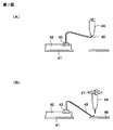
- 7 (A) and 7 (B) are cross-sectional views for explaining a conventional method of manufacturing a semiconductor device.
- FIG. 7A after the semiconductor element 42 is fixed on the die pad 41 of the lead frame, the lead frame is placed in a wire bonding apparatus.
- the electrode pad 43 of the semiconductor element 42 is heated to about 200 ° C., and the capillary 44 is moved onto the electrode pad 43.
- the metal ball formed at the tip of the capillary 44 is connected to the electrode pad 43 by the thermocompression bonding technique in combination with ultrasonic vibration. Generally this is called ball bonding.
- FIG. 7A after the semiconductor element 42 is fixed on the die pad 41 of the lead frame, the lead frame is placed in a wire bonding apparatus.
- the electrode pad 43 of the semiconductor element 42 is heated to about 200 ° C., and the capillary 44 is moved onto the electrode pad 43.
- the capillary 44 moves above the tip of the inner lead 46 and presses the fine metal wire 45 against the inner lead 46 with a desired load.
- the inner lead 46 is heated to about 200 ° C., and the thin metal wire 45 is connected to the inner lead 46 by a thermocompression bonding technique in combination with ultrasonic vibration.
- the capillary 44 ascends in a state where the wire clamper 47 is closed, and the thin metal wire 45 is broken at the connection point of the inner lead 46. Generally this is called stitch bonding.
- stitch bonding by repeating the wire bonding operation described in FIGS. 7A and 7B, all the electrode pads 43 of the semiconductor element 42 and the inner leads 46 are electrically connected by the fine metal wires 45.
- 17 (A) to 17 (C) are cross-sectional views for illustrating a conventional method of manufacturing a semiconductor device.
- the semiconductor chip 112 is mounted on the wiring substrate 111.
- a plurality of electrode pads 113 are disposed on the top surface of the semiconductor chip 112, and metal balls 115 formed at the tip of the capillary 114 are connected to the electrode pads 113.
- the capillary 114 ascends in a state where the wire clamper 116 is closed, and the thin metal wire 117 is cut from the metal ball 115.
- FIG. 17A the semiconductor chip 112 is mounted on the wiring substrate 111.
- a plurality of electrode pads 113 are disposed on the top surface of the semiconductor chip 112, and metal balls 115 formed at the tip of the capillary 114 are connected to the electrode pads 113.
- the capillary 114 ascends in a state where the wire clamper 116 is closed, and the thin metal wire 117 is cut from the metal ball 115.
- the capillary 114 is moved onto the metal ball 115 in a state where the fine metal wire 117 is led out from the tip of the capillary 114. Then, stitch bonding is performed on the metal ball 115, and the thin metal wire 117 drawn from the tip of the capillary 114 is connected to the metal ball 115. Thereafter, the capillary 114 moves above the wiring layer 118 in a state where the wire clamper 116 is open. Next, as shown in FIG. 17C, stitch bonding is performed on the wiring layer 118, and the fine metal wires 117 drawn from the tip of the capillary 114 are connected to the wiring layer 118. Thereafter, with the wire clamper 116 closed, the capillary 114 ascends and breaks the thin metal wire 117 at the connection point of the wiring layer 118
- the fine metal wires 45 are placed under high temperature during the wire bonding operation for all the electrode pads 43.
- the problem of oxidation was not regarded as important.
- a copper wire as the thin metal wire 45
- the copper wire is oxidized during the operation.
- the manufacturing method of the MAP (Matrix Array Packaging metod) method a large number of mounting portions are disposed on the lead frame. And, by increasing the number of wires to be wire-bonded, the working time becomes longer, and the above-mentioned oxidation problem is regarded as important.
- the die pad 41 and the inner leads 46 and the like also have a problem that they are oxidized by the above-described operation if the plating process or the like is not performed.
- wire bonding is performed in a state in which the plurality of inner leads 46 are collectively fixed by a clamper (not shown).
- a clamper not shown.
- the gold wire is soft and has a small ductility as compared with the copper wire. Therefore, the gold wire was easy to cut at the time of stitch bonding, and the fixation of the lead by the clamper was not particularly important.
- the gold wire has a specific resistance larger than that of the copper wire, the current capacity is small, and the use amount of the gold wire is increased in the semiconductor element handling a large current, which causes the problem of extra material cost.
- copper wire is harder than gold wire, for example, when ball bonding a copper ball directly to an electrode pad made of aluminum, the electrode pad softer than copper wire is pushed around the copper ball. , Splash around the copper ball. And the problem that the electrode pad which adjoins will short-circuit by the splash generate
- the electrode pad itself is made thin in order to prevent short circuit due to splash, damage to the insulating layer below the electrode pad is further increased as described above. Furthermore, most of the electrode pads on the bottom surface of the copper ball move as splash, reducing the connection area between the copper ball and the electrode pad, increasing the connection resistance or causing a connection failure.
- the present invention has been made in view of the above-described circumstances, and in the semiconductor device according to the present invention, the island, the plurality of leads disposed so as to surround the island, and the island are fixed via the adhesive.
- a semiconductor device comprising: a semiconductor element; a copper wire electrically connecting the electrode pad of the semiconductor element to the lead; and a resin package covering the island, the lead, the copper wire, and the semiconductor element.
- a plurality of through holes may be formed around the fixing area of the semiconductor element, and the through holes may be filled with a resin forming the resin package. Therefore, in the present invention, the material cost is reduced by using a copper wire. Then, the adhesion between the island and the resin package is improved by utilizing the through holes. Further, in the method of manufacturing a semiconductor device according to the present invention, a collective block including a plurality of mounting portions including an island, a plurality of leads arranged to surround the island, and a suspension lead extending from the island. A lead frame provided with a plurality of through holes is provided in the island, and a semiconductor element is fixed on the island, and then the electrode pad of the semiconductor element and the lead are wired with copper wires.
- the inert gas supplied to the mounting portion is positioned on a gas venting hole provided on a mounting table of the bonding apparatus, and Through the hole, characterized in that withdrawn from the gas vent hole. Therefore, in the present invention, the inert gas is likely to be filled around the wire-bonded copper wire, and the oxidation of the copper wire is prevented.
- an island a plurality of leads arranged to surround the island, a semiconductor element fixed on the island via an adhesive, an electrode pad of the semiconductor element, and
- a semiconductor device having a copper wire electrically connecting to a lead, and the resin package covering the island, the lead, the copper wire, and the semiconductor element, the copper wire is ball-bonded to the lead, and Stitch bonding is performed with gold balls formed on the electrode pads. Therefore, in the present invention, the material cost is reduced by using a copper wire. Then, by forming gold balls on the electrode pads, it is possible to prevent shorting of adjacent electrode pads.
- a collective block including a plurality of mounting portions including an island, a plurality of leads arranged to surround the island, and a suspension lead extending from the island.
- a lead frame provided with a plurality of through holes in each of the islands, a semiconductor element is fixed on the island, and gold balls are formed on electrode pads of the semiconductor element; Semiconductor bonding the gold balls and the leads by wire bonding with copper wires, completing the electrical connection in the aggregate block, covering the aggregate block with resin, forming a resin package, and singulating the resin package
- the through hole is positioned on a degassing hole provided on a mounting table of a wire bonding apparatus, The inert gas supplied to the mounting portion through the through-hole, characterized in that withdrawn from the gas vent hole.
- the inert gas is likely to be filled around the wire-bonded copper wire, and the oxidation of the copper wire is prevented.
- the material cost is reduced as compared to the case where a gold wire is used.
- the through holes of the island are buried by a part of the resin package, and the adhesion between the island and the resin package is improved.
- the inert gas supplied to the wire bonding area is drawn through the through holes formed in the island. And, by allowing the inert gas to be easily filled around the wire-bonded copper wire, the oxidation of the copper wire is prevented.
- the wire bonding operation is performed in a state where the plurality of leads are individually fixed by the clamper. And the relief of the load at the time of stitch bonding is prevented, and the cut portion of the copper wire is stabilized. Also, a good connection state can be realized. Further, in the present invention, by filling the resin to the through holes of the island and the back surface side of the suspension lead, it is possible to realize a structure in which the island is less likely to come off the resin package. Further, according to the present invention, by forming a gold ball on the electrode pad, it is possible to prevent shorting due to splash between adjacent electrode pads. Further, in the present invention, by forming the buffer material layer in the electrode pad, it is possible to prevent the occurrence of a crack in the insulating layer on the lower surface of the electrode pad.
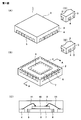
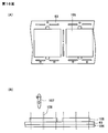
- FIG. 1 is a view for explaining a semiconductor device according to an embodiment of the present invention
- FIG. 1 (A) is a perspective view
- FIG. 1 (B) is a perspective view
- FIG. (C) is a cross-sectional view
- FIG. 1 (D) is a perspective view
- FIG. 1 (E) is a perspective view
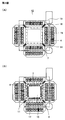
- FIG. 2 explains a semiconductor device according to an embodiment of the present invention.
- 2 (A) is a plan view
- FIG. 2 (B) is a plan view
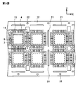
- FIG. 3 explains a method of manufacturing a semiconductor device according to an embodiment of the present invention.
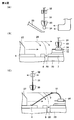
- 4 (A) is a plan view for explaining the method of manufacturing a semiconductor device according to the embodiment of the present invention
- FIG. 4 (A) is a plan view.
- FIG. 5 is a cross-sectional view
- FIG. 5 is a view for explaining a method of manufacturing a semiconductor device according to an embodiment of the present invention
- FIG. 5 (A) is a cross-section 5 (B) is a cross-sectional view
- FIG. 5 (C) is a cross-sectional view
- FIG. 6 is a view for explaining a method of manufacturing a semiconductor device according to an embodiment of the present invention.
- 6 (A) is a plan view
- FIG. 6 (B) is a cross-sectional view
- FIG. 7 is a view for explaining a method of manufacturing a semiconductor device according to a conventional embodiment.
- 7 (A) is a sectional view
- FIG. 7 (B) is a sectional view
- FIG. 8 is a view for explaining a semiconductor device according to another embodiment of the present invention
- 8 (A) is a perspective view
- FIG. 8 (B) is a perspective view
- FIG. 8 (C) is a cross-sectional view
- FIG. 8 (D) is a perspective view
- (E) is a perspective view
- FIG. 9 is a view for explaining a semiconductor device according to another embodiment of the present invention
- FIG. 9 (A) is a plan view
- FIG. 10 is a plan view
- FIG. 10 is a view for explaining a semiconductor device according to another embodiment of the present invention
- FIG. 10 (A) is a cross sectional view
- FIG. 10 (B) is a cross sectional view
- FIG. 10 (B) is a cross sectional view
- FIG. 11 is a view for explaining a semiconductor device according to another embodiment of the present invention
- FIG. 11 (A) is a cross-sectional view
- FIG. 11 (B) is a cross-sectional view
- FIG. 12 is a view for explaining a semiconductor device according to another embodiment of the present invention
- FIG. 12 (A) is a sectional view
- FIG. 12 (B) is a sectional view
- FIG. 13 is a plan view for explaining a method of manufacturing a semiconductor device in another embodiment of the present invention
- FIG. 14 is a diagram for explaining a method of manufacturing a semiconductor device in another embodiment of the present invention.
- FIG. 14 (A) is a plan view
- FIG. 14 (B) is a cross-sectional view
- FIG. 15 is a diagram for explaining a method of manufacturing a semiconductor device in another embodiment of the present invention
- FIG. 15 (A) is a cross-sectional view
- FIG. 15 (B) is a cross-sectional view
- FIG. FIG. 16C is a cross-sectional view
- FIG. 16 is a view for explaining a method of manufacturing a semiconductor device in another embodiment of the present invention
- FIG. 16A is a plan view
- FIG. 16 (B) is a cross-sectional view
- FIG. 17 is a view for explaining a method of manufacturing a semiconductor device in the conventional embodiment
- FIG. 17 (A) is a cross-sectional view
- FIG. (B) is a cross-sectional view
- FIG. 17 (C) is a cross-sectional view.
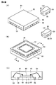
- FIG. 1 (A), (B), (D) and (E) are perspective views for explaining a resin package.
- FIG. 1 (C) is a cross-sectional view for explaining a resin package.
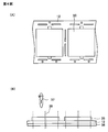
- FIG. 2 (A) is a plan view for explaining a lead frame.
- FIG. 2 (B) is a figure which shows the condition which carried out the wire bonding to FIG. 2 (A).
- the semiconductor device 1 comprises, for example, a resin package 2 of the MAP system.
- the leads 4 are exposed from the side surface 3 of the resin package 2 in order to be singulated by dicing.
- the exposed leads 4 form the same surface as the side surface 3 of the resin package 2.
- the exposed shape of the lead 4 is not limited to the illustrated shape.
- the exposed shape of the leads 4 may be T-shaped.
- the dicing region on the back surface side of the lead 4 is half-etched and the exposed surface of the lead 4 is separated from the side 5 of the resin package 2 to the surface side of the resin package 2 But it is good.
- the island 7 is exposed on the back surface 6 of the resin package 2 and this island 7 forms substantially the same surface as the back surface 6 of the resin package 2.
- FIG. 1 (C) is a cross-sectional view taken along the line A-A shown in FIG. 1 (B), and is a cross-section including the through holes 8 formed in the island 7.
- the semiconductor element 10 is fixed on the island 7 by an adhesive 9 such as Ag paste or solder, for example.
- the electrode pad of the semiconductor element 10 and the lead 4 are electrically connected by the copper wire 11 which is the subject of the present invention.
- the copper wire 11 is made of, for example, 33 to 50 ⁇ m in diameter and 99.9 to 99.99 wt% of copper.
- the copper wire 11 is ball-bonded onto the electrode pad of the semiconductor element 10 and stitch-bonded onto the lead 4.
- the diameter of the copper wire 11 can be arbitrarily changed in design in accordance with the application to be used.
- the island 7 is made of, for example, a frame whose main material is copper having a thickness of about 100 to 250 ⁇ m, and a plurality of through holes 8 are formed in the island 7.
- the through holes 8 are used as a flow path of an inert gas (forming gas) at the time of die bonding or wire bonding, the through holes 8 are arranged in the outer peripheral region of the fixing region of the semiconductor element 10. Then, at the time of resin molding, the through holes 8 are buried by the insulating resin. By this structure, the contact area between the resin package 2 and the island 7 is increased, the resin enters the island 7, and the island 7 is firmly supported in the resin package 2. In the resin package 2, for example, low-molecular components contained in the resin package 2 and the adhesive 9 are vaporized by the driving heat of the semiconductor element 10 or the like to generate a gas.
- the gas receives an external force in a direction in which the island 7 is pushed out of the resin package 2 by the gas.
- the adhesion between the island 7 and the resin package 2 is weak, and the island 7 is easily pushed out of the resin package 2 by the gas. Therefore, by improving the degree of adhesion between the resin package 2 and the island 7 in a circular manner around the island 7, the island 7 is less likely to come off the resin package 2.
- the through hole 8 is also used as a discharge path of the gas generated in the resin package 2, particularly around the island 7.
- a frame mainly made of copper is generally used as the lead frame 12, but a frame mainly made of Fe-Ni may be used, and other metal materials may be used. Even when it consists of.
- a plurality of mounting portions 13 indicated by alternate long and short dash lines are formed on the lead frame 12 made of these materials. Although one mounting portion 13 is shown in the figure, as shown in FIG. 3, for example, one collective block is formed by gathering four of the mounting portions 13. Then, resin molding is integrally performed on each of the collective blocks.
- the mounting portion 13 mainly includes the island 7, the suspension leads 14 supporting the island 7, the leads 4 located in the vicinity of four sides of the island 7, and the tie bars 15 supporting the plurality of leads 4. Be done. And, the suspension leads 14 extend from the four corners of the island 7 and connect with the cross support areas 16 of the tie bars 15.
- the support area 16 is integral with the lead frame 12 and the island 7 is supported by the lead frame 12. Then, since the region shown by the dotted line in the island 7 becomes the fixing region of the semiconductor element 10, the through hole 8 which is the point of the present invention is arranged at a position surrounding the fixing region. Further, the hatched area of the suspension lead 14 is etched by about 0.05 to 0.15 ⁇ m from the back surface side of the lead frame 12 to become a recessed area.
- the recessed area of the suspension lead 14 is filled with a resin, and the suspension lead 14 is supported by the resin package 2 to obtain an anchor effect. Then, the gas generated in the resin package 2 and the adhesive 9 may receive an external force that pushes the island 7 out of the resin package 2. In this case, the island 7 is supported in the resin package 2 by the suspension leads 14, and the island 7 does not easily come off the resin package 2. As shown in FIG. 1 (B), the suspension leads 14 are not exposed from the back surface 6 of the resin package 2. Further, the hatched area of the lead 4 is also etched from, for example, about 0.05 to 0.18 ⁇ m from the back surface side of the lead frame 12 to become a recessed area. And the recessed area shown by hatching becomes a dicing line.
- the lead frame 12 can be easily divided into individual resin packages 2.
- the semiconductor element 10 is fixed on the island 7, and the electrode pad 17 and the lead 4 are electrically connected by the copper wire 11. Then, it is necessary to prevent the oxidation of the connection portion between the copper wire 11 or the copper wire 11 and the electrode pad 17 or the like.
- the inert gas flows from the upper side to the bonding area from the upper side by the structure where the inert gas is drawn out from the through hole 8, and the arrangement area of the copper wire 11 is always It becomes easy to be filled with inert gas.
- the copper wire 11 is a material which is easy to oxidize, the oxidation is prevented by the existence of inactive gas.
- the copper wire 11 can be used as the wire bonding material in place of the gold wire which is an inert and stable material, and the material cost can be reduced by using the copper wire.
- the shape of the through hole 8 is circular, oval or rectangular, and the width of the through hole 8 is equal to or larger than the separation width between the adjacent leads 4.
- the through hole 8 becomes a flow path of the inert gas, whereby the oxidation of the side surface of the through hole 8 is prevented, and the adhesion with the insulating resin in which the through hole 8 is embedded is also improved.
- a semiconductor device that handles a large current
- a gold wire a plurality of gold wires are used for one electrode pad to cope with a large current, but in the case of a copper wire, the resistance is small. Since the current capacity is large, it can cope with a large current with a smaller number than in the case of the gold wire. As a result, the area of the bonding region can be made smaller than in the case of the gold wire, and miniaturization of the semiconductor element can be realized.
- the MAP type resin package 2 has been described, but the present invention is not limited to this package.
- individual mold type packages such as QFP (Quad Flat Package) type packages and QFN (Quad Flat Non-leaded Package) type packages
- wires made of copper wire can be provided by providing through holes in the islands. Bonding is possible, and the same effects as described above can be obtained.
- various modifications can be made without departing from the scope of the present invention.
- FIG. 3 is a plan view for explaining the lead frame.
- FIG. 4 (A) is a plan view for explaining a clamper.
- FIG. 3 is a plan view for explaining the lead frame.
- FIG. 4 (A) is a plan view for explaining a clamper.
- FIG. 4 (B) is a cross-sectional view for explaining the flow of the inert gas at the time of wire bonding.
- 5 (A) to 5 (C) are cross-sectional views for explaining a wire bonding process.
- FIG. 6 (A) is a plan view for explaining a resin molding process.
- FIG. 6 (B) is a cross-sectional view for explaining a dicing process.
- the same components as those of the semiconductor device described with reference to FIGS. 1 and 2 are denoted by the same reference numerals.
- FIG. 1 and FIG. 2 it will be described using FIG. 1 and FIG. 2 as appropriate.
- a lead frame 12 mainly made of copper is prepared.
- a plurality of mounting portions 13 are formed on the lead frame 12 as indicated by alternate long and short dash lines.
- the longitudinal direction of the lead frame 12 (in the X-axis direction in the drawing) is divided by the slits 21 at regular intervals.
- one collective block composed of a set of four mounting parts 13 is formed in one section of the lead frame 12 divided by the slits 21, for example.
- a plurality of the collective blocks are formed in the longitudinal direction of the lead frame 12.
- index holes 22 are provided at constant intervals in the upper and lower end regions thereof, and are used for positioning in each process.
- the detailed structure of the mounting portion 13 is as described in FIG. 2 (A).
- the area indicated by the dotted line in FIG. 3 is the arrangement area of the gas venting holes 29 of the mounting table 23.
- the gas venting holes 29 of the mounting table 23 For example, on one gas venting hole 29.
- a plurality of through holes 8 are arranged.
- the semiconductor elements 10 are continuously fixed on the plurality of islands 7.
- the details are the same as the flow of the inert gas in the wire bonding step described in FIG. 4 (B), but the inert gas flows into the working area from the clamper fixing the lead frame 12.
- the inert gas is drawn to the mounting table side through the through holes 8 of the island 7, whereby the periphery of the lead frame 12 is filled with the inert gas.
- the lead frame 12 is mainly made of copper and is placed under high temperature conditions for a long time, but its oxidation is prevented.
- the lead frame 12 is disposed on the mounting table 23 of the wire bonding apparatus. Wire bonding is performed every 13.
- the clamper 24 shown in FIG. 4 (A) will be described.
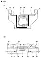
- the clamper 24 has a pipe 25 for feeding an inert gas, and an opening area 26 opened in accordance with the size of the mounting portion 13. Then, the inert gas blown from the pipe 25 of the clamper 24 is blown into the opening area 26 from between the lead fixing areas 27.
- nitrogen gas including some hydrogen gas
- the copper wire 11 is easily oxidized by being placed in the high temperature working area, but the oxidation of the copper wire 11 is prevented by the presence of the inert gas. Furthermore, in the clamper 24 around the opening area 26, a plurality of lead fixing areas 27 are arranged in a comb-tooth shape in accordance with the shape of the leads 4 of the mounting portion 13. Then, the plurality of leads 4 are individually fixed on the mounting table 23 (see FIG. 4B) by the lead fixing regions 27. At the lead 4 side, wire bonding stitch bonding is performed. At this time, the copper wire 11 is harder than a gold wire, but has ductility. Therefore, the load at the time of stitch bonding (the load applied from the capillary 30 (see FIG.
- the plurality of leads 4 are individually fixed by the lead fixing regions 27 of the clamper 24 corresponding to the respective shapes, so that the relief of the load at the time of the stitch bonding is prevented. Then, the copper wire 11 is cut in a state in which the copper wire 11 is securely adhered on the lead 4, and the cut portion of the copper wire 11 is stabilized, whereby the shape of the copper wire 11 after cutting is also stabilized. Next, the flow of the inert gas shown in FIG. 4 (B) will be described. A gas venting hole 29 is formed in the mounting table 23 having the heating mechanism 28.
- the lead frame 12 is disposed on the mounting table 23 so that the through holes 8 of the island 7 are positioned on the upper surface of the gas venting hole 29.
- the inert gas is blown from between the lead fixing regions 27 of the clamper 24 to the center side (mounting portion) of the opening region 26. That is, in the opening area 26, the inert gas is blown from the entire periphery to the center side.
- the opening region 26 is not capped, and the inside of the opening region 26 is in a high temperature state, so that the inert gas is released above the opening region 26 by the upward air flow.
- the inert gas blown from the side of the lead 4 by suctioning the inert gas from the degassing holes 29 of the mounting table 23 through the through holes 8 mainly corresponds to that of the island 7. It flows to the through hole 8 side.
- the main flow of the inert gas is on the lower side of the opening area 26 (on the side of the mounting table 23), and the arrangement area of the copper wire 11 is an area easily filled with the inert gas.
- the heating mechanism 28 maintains the inside of the working area inside the opening area 26 of the clamper 24 at, for example, about 250 ° C. to 260 ° C.
- the wire bonding of the copper wire 11 is high temperature until the wire bonding is completed to all the electrode pads of the semiconductor device 10 (for example, the wire bonding is completed to all the semiconductor devices 10 in one collective block) Placed in the working area of the state. Therefore, by causing the above-described flow of the inert gas, the periphery of the copper wire 11 is easily filled with the inert gas, and the oxidation of the copper wire 11 is efficiently prevented. Further, although the lead frame 12 such as the leads 4 is also easily oxidized, the inert gas flows toward the mounting table 23 so that the lead frame 12 is also efficiently prevented from being oxidized.
- the inert gas blown into the opening area 26 is not sucked from the degassing holes 29 of the mounting table 23, and a part of the inert gas flows above the opening area 26. Then, the opening region 26 and the periphery thereof become a region filled with the inert gas.
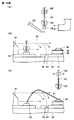
- the copper wire 31 is inserted into the center hole of the capillary 30, and a wire clamper 32 for clamping the copper wire 31 is disposed above the capillary 30.
- the wire clamper 32 is opened, a copper wire 31 having a desired length is drawn from the tip of the capillary 30, and discharged from the torch 33 located in the vicinity of the capillary 30, and the initial ball 34 is formed at the tip of the capillary 30. Be done.
- a current of, for example, 125 mA is required when forming the initial ball 34.
- a current of 75 mA is required when forming an initial ball using a gold wire of the same diameter.
- the copper wire 31 is a material having high thermal conductivity and excellent heat dissipation compared to the gold wire, and the copper wire 31 is easily cooled by the inert gas.
- the inert gas is supplied to the work area where the initial ball 34 is formed. Therefore, the spherical shape of the initial ball 34 is stably formed by the oxidation-reduction action by hydrogen contained in the inert gas.
- FIG. 5 (B) the capillary 30 descends onto the electrode pad 17 of the semiconductor element 10 and presses the initial ball 34 against the upper surface of the electrode pad 17.
- the initial ball 34 formed at the tip of the capillary 30 is connected to the electrode pad 17 by the thermocompression bonding technique in combination with ultrasonic vibration.
- the wire clamper 32 is in an open state.
- the capillary 30 is moved to the upper surface of the lead 4 while drawing a fixed loop in a state where the wire clamper 32 is opened.
- the capillary 30 descends onto the lead 4 and presses the copper wire 31 against the upper surface of the lead 4.
- the copper wire 31 is connected to the lead 4 by the thermocompression bonding technique in combination with ultrasonic vibration. Thereafter, the capillary 30 ascends to cut the copper wire 31.
- the common resin package 35 is cut from the lead frame 12 for each mounting portion 13 into individual resin packages 2.
- the common resin package 35 and the lead frame 12 are simultaneously diced along the dicing lines 38 using the dicing blade 37 of the dicing apparatus.
- the dicing blade 37 of the dicing apparatus is simultaneously diced along the dicing lines 38 using the dicing blade 37 of the dicing apparatus.
- the hatching area of the lead 4 shown in FIG. 2 (A) is disposed on the dicing line. Then, by cutting the recessed area of the lead 4 with the dicing blade 37, the load on the dicing blade 37 is reduced and the long-term use becomes possible.
- the temperature of the inert gas to be blown is not particularly limited.
- the inert gas may be heated and then blown into the opening region 26.
- the copper wire 31 is not easily cooled by the inert gas, and the current efficiency at the time of initial ball formation can be improved.
- the lid member such as a plate
- the lid member may slide in accordance with the working area.
- the upper part of the opening area 26 is generally covered by the lid member, so that the inside of the opening area 26 is easily filled with the inert gas. And the supply amount of inert gas is also reduced, and the effect that the manufacturing cost can be suppressed is also obtained.
- the present invention is not limited to this case. For example, when individual leads can be firmly fixed according to the lead configuration and the lead arrangement situation such as the height of the leads, the adjacent plural leads may be divided and fixed by the lead fixing area. .
- FIGS. 8 (A), (B), (D) and (E) are perspective views for explaining a resin package.
- FIG. 8 (C) is a cross-sectional view for explaining a resin package.
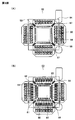
- FIG. 9 (A) is a plan view for explaining a lead frame.
- FIG. 9 (B) is a plan view for explaining the situation where wire bonding is performed on the lead frame.
- the semiconductor device 51 comprises, for example, a resin package 52 of the MAP system.
- the leads 54 are exposed from the side surface 53 of the resin package 52 in order to singulate by dicing. Then, the exposed leads 54 form the same surface as the side surface 53 of the resin package 52.
- the exposed shape of the lead 54 is not limited to the illustrated shape. For example, as shown in FIG.
- the exposed shape of the lead 54 may be T-shaped. Further, as shown in FIG. 8E, the dicing region on the back surface side of the lead 54 is half-etched, and the exposed surface of the lead 54 is separated from the side 55 of the resin package 52 to the surface side of the resin package 52 But it is good. As shown in FIG. 8B, the island 57 is exposed on the back surface 56 of the resin package 52, and the island 57 forms substantially the same surface as the back surface 56 of the resin package 52. Then, a plurality of through holes 58 are formed in the outer peripheral region in the island 57, and the through holes 58 are filled with the insulating resin constituting the resin package 52.
- FIG. 8C shows a cross-sectional view in the direction of the line B-B shown in FIG. 8B, and is a cross section including the through holes 58 formed in the island 57.
- the semiconductor element 60 is fixed on the island 57 by an adhesive 59 such as Ag paste or solder.
- a plurality of electrode pads 68 are formed on the upper surface of the semiconductor element 60, and gold balls 62 are formed on the upper surface of the electrode pad 68.
- the gold ball 62 and the inner lead portion of the lead 54 are connected by the copper wire 61, which is the subject matter of the present invention.
- the copper wire 61 is made of, for example, copper having a diameter of 33 to 50 ⁇ m and 99.9 to 99.99 wt%. Then, as illustrated, the copper wire 61 is ball bonded onto the lead 54 and stitch bonded onto the gold ball 62 of the electrode pad 68.
- the diameter of the copper wire 61 can be arbitrarily changed in design depending on the application to be used.
- the island 57 is, for example, a frame whose main material is copper having a thickness of about 100 to 250 ⁇ m, and a plurality of through holes 58 are formed in the island 57.
- the through holes 58 are used as a flow path of an inert gas (forming gas) at the time of die bonding or wire bonding, the through holes 58 are disposed in the outer peripheral region of the fixing region of the semiconductor element 60. Then, at the time of resin molding, the through holes 58 are buried by the insulating resin. By this structure, the contact area between the resin package 52 and the island 57 is increased, the resin enters the island 57, and the island 57 is firmly supported in the resin package 52. Furthermore, since the through holes 58 serve as a flow path for the inert gas, oxidation of the side surfaces of the through holes 58 is prevented, and the degree of adhesion between the island 57 and the resin package 52 is improved.
- an inert gas forming gas
- the resin package 52 low molecular weight components contained in the resin package 52 and the adhesive 59 are vaporized by the driving heat of the semiconductor element 60 or the like to generate gas.
- the gas receives an external force in a direction in which the island 57 is pushed out of the resin package 52 by the gas.
- the thickness of the island 57 is as thin as 100 to 250 ⁇ m, the degree of adhesion between the island 57 and the resin package 52 is weak, and the island 57 is easily pushed out of the resin package 52 by the gas.
- the through holes 58 in the outer peripheral region of the island 57, the degree of adhesion between the resin package 52 and the island 57 is improved, and the island 57 is less likely to come off from the resin package 52.
- the through hole 58 is also used as a discharge path of the gas generated in the resin package 52, particularly around the island 57.
- the island 57 is unlikely to be pushed out of the resin package 52 by the gas.
- a frame mainly made of copper is generally used as the lead frame 63, but a frame mainly made of Fe-Ni may be used, and other metal materials may be used. Even when it consists of.
- a plurality of mounting portions 64 indicated by alternate long and short dash lines are formed on the lead frame 63 made of these materials. Although one mounting portion 64 is shown in the figure, as shown in FIG.
- the mounting portion 64 mainly includes an island 57, a suspension lead 65 for supporting the island 57, a lead 54 whose one end is located near four sides of the island 57, and a tie bar 66 for supporting a plurality of leads 54. And consists of And, the suspension leads 65 extend from the four corners of the island 57 and connect with the cross support areas 67 of the tie bars 66.
- the support region 67 is integral with the lead frame 63, and the island 57 is supported by the lead frame 63.
- a region indicated by a dotted line in the island 57 is a fixing region of the semiconductor element 60, and the through holes 58 are arranged so as to surround the fixing region.
- two through holes 58 are disposed along one side of the island 57, and the length of the through hole 58 is about half the length of one side of the island 57.
- the details will be described later with reference to FIG. 14 (B).
- the through hole is enlarged even when the lead frame is slightly deviated by the increase of the opening area of the through hole 58.
- the degassing holes 99 are easily disposed below the portion 58, and the suction force of the inert gas can be properly maintained.
- the shape of the through hole 58 is not limited to the illustrated shape.
- the shape of the through hole 58 may be, for example, circular, oval or rectangular, and the through hole 58 has a width equal to or larger than the separation width between the adjacent leads 54 good.
- the hatched area of the suspension lead 65 is etched by about 0.05 to 0.15 ⁇ m from the back surface side of the lead frame 63 to become a recessed area. Then, the recessed area of the suspension lead 65 is filled with resin, the suspension lead 65 is supported by the resin package 52, and an anchor effect is obtained.
- the gas generated in the resin package 52 and the adhesive 59 may receive an external force that pushes the island 57 out of the resin package 52.
- the island 57 is supported in the resin package 52 by the suspension lead 65, and the island 57 is not easily detached from the resin package 52.
- the suspension leads 65 are not exposed from the back surface 56 of the resin package 52.
- the semiconductor element 60 is fixed on the island 57, and a gold ball 62 is formed on the upper surface of the electrode pad 68.
- the copper wire 61 is ball bonded to the upper surface of the lead 54 and then stitch bonded to the upper surface of the gold ball 62.
- the inert gas flows from the upper side to the bonding area from the upper side by the structure of extracting the inert gas from the through hole 58, and the arrangement area of the copper wire 61 is always It is easily filled with an inert gas and its oxidation is prevented by the presence of the inert gas.
- the copper wire 61 can be used in place of the gold wire, and the cost can be significantly reduced.
- multiple gold wires are used for one electrode pad to cope with large currents.
- a silicon oxide film, a boron phosphosilicate glass (BPSG) film, a tetra-ethyl-orso-silicate (TEOS) film or a spin on glass (SOG) film is formed on a silicon substrate 69.
- An insulating layer 70 such as a film is formed.
- an electrode pad 68 is formed on the insulating layer 70, and the film thickness of the electrode pad 68 is, for example, 0.4 to 3.0 ⁇ m.
- the electrode pad 68 is formed of, for example, an aluminum layer or an alloy layer mainly composed of aluminum.
- the alloy layer is, for example, an aluminum-silicon film, an aluminum-silicon-copper film, an aluminum-copper film or the like.
- a shield layer 71 made of, for example, a silicon nitride film is formed on the insulating layer 70, and an opening 72 is formed in the shield layer 71 on the electrode pad 68.
- the above-described alloy layer is mainly made of aluminum, and silicon, copper and the like are substantially uniformly arranged in the aluminum.
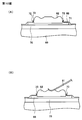
- Gold balls 62 are ball bonded on the electrode pads 68 exposed from the openings 72. Then, the gold ball 62 slightly bites into the electrode pad 68 due to the load at the time of ball bonding, and a slight splash 73 may occur around the gold ball 62. However, the gold ball 62 is soft compared to the copper ball, and the load at bonding is smaller than that of the copper ball. Therefore, the splash 73 is generated between the side surface of the opening 72 and the gold ball 62 and does not occur beyond the formation area of the electrode pad 68. With this structure, the splashes 73 do not contact each other on the adjacent electrode pads 68 and do not short.
- the gold ball 62 may be connected on the electrode pad 68 only by the thermocompression bonding technique without using the ultrasonic vibration technique.
- the generation of the splash 73 described above can be minimized. it can.
- the bonding load can be adjusted by reducing the size of the gold ball 62, and the generation of the splash 73 described above can be minimized.
- the electrode pad 68 sufficiently remains between the bottom of the gold ball 62 and the insulating layer 70. According to this structure, the bottom surface of the gold ball 62 is in a state of being securely connected to the electrode pad 68, and an increase in connection resistance value at the electrode pad 68 can be prevented. Also, connection failure at the electrode pad 68 can be prevented.
- the copper wire 61 is stitch-bonded onto the gold ball 62.
- the load at the time of bonding of the copper wire 61 is dispersed by the gold ball 62. That is, the gold ball 62 is used as a buffer material, and it is possible to prevent damage such as a crack on the insulating layer 70 below the electrode pad 68 due to an impact at the time of bonding.
- the dispersion of the bonding load prevents the splash 73 from being significantly increased, and is slightly larger than the splash 73 generated when the gold ball 62 is connected as shown in FIG. 10A.
- the electrode pads 68 adjacent to each other due to the splash 73 are not short-circuited. Furthermore, the copper wire 61 is stitch-bonded onto the gold ball 62, so that the height above the semiconductor element 60 is suppressed, and thinning of the resin package 52 is realized. On the other hand, although not shown, the copper wire 61 is ball-bonded onto the lead 54, whereby the connection area with the lead 54 is increased more than the stitch bonding. As a result, even when the thickness of the lead 54 is reduced, the lead 54 is less likely to be bent by an impact at the time of bonding, and a further reduction in thickness of the resin package 52 is realized.
- the copper wire 61 may be stitch-bonded to the gold ball 62 and the lead 54, or may be ball-bonded to the gold ball 62 and stitch-bonded to the lead 54. Also in these cases, as described above, the short circuit by the splash 73 is prevented, and the damage to the insulating layer 70 is also prevented.
- FIG. 11 and FIG. 12 without using the gold ball 62 (see FIG. 10), the structure of the electrode pad corresponds to the problem of short due to splash and the problem of cracks in the insulating layer.
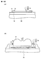
- the electrode pad 74 has a structure in which the buffer material layer 76 is disposed between the aluminum layers 75 and 77.
- the film thickness of the aluminum layer 75 is about 0.4 ⁇ m
- the film thickness of the buffer material layer 76 is about 0.1 ⁇ m
- the film thickness of the aluminum layer 77 is about 2 to 9 ⁇ m.
- the film thickness of 74 is about 3.4 ⁇ m.
- the buffer material layer 76 is a film harder than the aluminum layers 75 and 77, and is formed of, for example, a refractory metal layer such as a titanium nitride (TiN) layer or a titanium tungsten (TiW) layer.
- a refractory metal layer such as a titanium nitride (TiN) layer or a titanium tungsten (TiW) layer.
- an alloy layer mainly composed of aluminum may be disposed on the upper and lower surfaces of the buffer material layer 76. As shown in FIG.
- the buffer material layer 76 is disposed on the aluminum layer 75, so that the structure is difficult to be removed around the copper ball 78 at the time of bonding. As a result, the aluminum layer 75 reliably exists on the bottom surface of the copper ball 78, and connection failure at the electrode pad 74 is prevented. Furthermore, by arranging the buffer material layer 76 between the aluminum layers 75 and 77, the bonding load can be relieved by the buffer material layer 76, and damage to the insulating layer 70 below the electrode pad 74 can be prevented. . Furthermore, the shock-absorbing material layer 76 is fractured by the bonding load, whereby the aluminum layers 75 and 77 are directly connected in the fractured area.
- the electrode pad 80 is formed by forming the buffer material layer 81 on the upper surface of the insulating layer 70 and arranging the aluminum layer 82 so as to cover the buffer material layer 81.
- the buffer material layer 81 is disposed inward of the opening 72 of the shield layer 71 and has a width W2 smaller than the width W1 of the opening 72.
- the shape of the shock absorbing material layer 81 is a shape in which the shape of the opening 72 is similarly reduced.
- the thickness of the buffer material layer 81 is, for example, 0.5 to 1.0 ⁇ m
- the thickness of the aluminum layer 82 is, for example, 0.4 to 3.0 ⁇ m.
- the above-described protruding region may be formed on the electrode pad 80, and the buffer material layer 81 may be disposed in the aluminum layer as in the structure of FIG.
- copper balls 83 are ball bonded onto the electrode pads 80 exposed from the openings 72 of the shield layer 71. Then, due to the load at the time of ball bonding, the copper ball 83 slightly bites into the electrode pad 80, and a splash 84 is generated around the copper ball 83.
- the copper ball 83 is ball-bonded to the protruding area of the electrode pad 80, whereby the aluminum layer 82 in the protruding area is driven to the side of the opening 72 as shown by the dotted arrow.
- the driven aluminum layer 82 first moves to a recessed area 85 (see FIG. 12A) around the protruding area, and embeds the recessed area 85. Then, the aluminum layer 82 overflowing from the recessed area 85 becomes the splash 84, and the splash 84 itself becomes smaller. With this structure, the splashes 84 can be prevented from coming into contact and shorting at adjacent electrode pads 80. Furthermore, since the buffer material layer 81 is disposed in the region where the copper balls 83 are ball bonded, the bonding load is relaxed by the buffer material layer 81 and damages such as cracks are caused to the insulating layer 70 below the electrode pad 80. Can be prevented.
- a plurality of through holes 58 are formed in the island 57, and the flow of the inert gas is adjusted through the through holes 58 to prevent the oxidation of the copper wire 61 and the connection region thereof.
- the flow of the inert gas may be adjusted by utilizing the gap between the island 57 and the lead 54 or the gap between the leads 54.
- the flow of the inert gas described above may be adjusted by using the through holes 58 in combination with the aforementioned gaps.
- FIGS. 13A and 13B are plan views for explaining the lead frame.
- FIG. 14 (A) is a plan view for explaining a clamper.
- FIG. 14 (B) is a cross-sectional view for explaining the flow of the inert gas at the time of wire bonding.
- FIG. 15 (A) to 15 (C) are cross-sectional views for explaining a wire bonding step.
- FIG. 16 (A) is a plan view for explaining a resin molding process.
- FIG. 16 (B) is a cross-sectional view for explaining the dicing step.
- the same components as those of the semiconductor device described with reference to FIGS. 8 to 10 are denoted by the same reference numerals. Further, in the description of the manufacturing method of the present embodiment, the description will be made using FIGS. 8 to 10 as appropriate.
- a lead frame 63 mainly made of copper is prepared.
- a plurality of mounting portions 64 are formed on the lead frame 63, as indicated by an alternate long and short dash line.
- the longitudinal direction of the lead frame 63 (in the X-axis direction in the drawing) is divided by the slits 91 at regular intervals. Then, in one section of the lead frame 63 divided by the slits 91, for example, one collective block consisting of a set of four mounting parts 64 is formed. Then, a plurality of the collective blocks are formed in the longitudinal direction of the lead frame 63. In the longitudinal direction of the lead frame 63, index holes 92 are provided at constant intervals in the upper and lower end regions thereof, and are used for positioning in each process.
- the detailed structure of the mounting portion 64 is as described in FIG. 9 (A). Further, although described later with reference to FIG. 14 (B), the area indicated by the dotted line in FIG.
- the degassing holes 99 are larger than the through holes 58.
- the space between the island 57 and the lead 54 or the space between the leads 54 may be used to draw out the inert gas.
- the semiconductor element 60 is fixed on the island 57 using the adhesive 59 (see FIG. 8C) for each mounting portion 64 of the lead frame 63.
- the lead frame 63 is disposed on the mounting table of the die bonding apparatus in which the heating mechanism is incorporated, and the lead frame 63 is fixed on the mounting table by the clamper.
- the semiconductor element 60 is continuously fixed on the island 57.
- the inert gas flows into the working area from the clamper fixing the lead frame 63. Then, the inert gas is drawn to the mounting table side through the through holes 58 of the island 57, whereby the periphery of the lead frame 63 is filled with the inert gas. As a result, the lead frame 63 is placed under a high temperature condition for a long time, but its oxidation is prevented. Next, the lead frame 63 is disposed on the mounting table 93 of the wire bonding apparatus, and wire bonding is performed for each mounting portion 64 of the lead frame 63. First, the clamper 94 shown in FIG. 14 (A) will be described.
- the clamper 94 has a pipe 95 for feeding an inert gas, and an opening area 96 opened to the size of the mounting portion 64. Then, the inert gas blown from the pipe 95 of the clamper 94 is blown into the opening area 96 from between the lead fixing areas 97.
- nitrogen gas including some hydrogen gas
- the copper wire 61 is easily oxidized by being placed in the high temperature work area, but the oxidation of the copper wire 61 is prevented by the presence of the inert gas.
- a plurality of lead fixing areas 97 are arranged in a comb-tooth shape in accordance with the shape of the leads 54 of the mounting portion 64.
- the plurality of leads 54 are individually fixed on the mounting table 93 (see FIG. 14 (B)) by the lead fixing regions 97.
- the copper wire 61 is harder than a gold wire, but has ductility, so the load at the time of ball bonding (the load applied from the capillary 100 (see FIG. 15 (A)) becomes larger than the gold wire.
- the plurality of leads 54 are individually fixed by the lead fixing regions 97 of the clampers 94 corresponding to the respective shapes, so that the escape of the load at the time of bonding is prevented.
- a gas venting hole 99 is formed in the mounting table 93 having the heating mechanism 98.
- the lead frame 63 is disposed on the mounting table 93 so that the through holes 58 of the island 57 are positioned on the upper surface of the gas venting hole 99.
- the inert gas is blown from between the lead fixing regions 97 of the clamper 94 to the center side (mounting portion) of the opening region 96. That is, in the opening area 96, the inert gas is blown from the entire periphery to the center side.
- the opening area 96 is not shielded and the inside of the opening area 96 is in a high temperature state, so that the inert gas is released above the opening area 96 by the upward air flow. Therefore, in the present embodiment, the inert gas blown from the top of the lead 54 is mainly the island 57, by sucking the inert gas from the gas vent holes 99 of the mounting table 93 through the through holes 58. Flow to the through hole 58 side of the As a result, the main flow of the inert gas is on the lower side (the mounting table 93 side) of the opening area 96, and the arrangement area of the copper wire 61 is an area which is easily filled with the inert gas.
- the inside of the open area 96 of the clamper 94 is maintained at, for example, about 250 to 260 ° C. by the heating mechanism 98.
- the wire bonding of the copper wire 61 is high temperature until the wire bonding is completed to all the electrode pads of the semiconductor device 60 (for example, the wire bonding is completed to all the semiconductor devices 60 in one collective block) Placed in the working area of the state. Therefore, by causing the above-described flow of the inert gas, the periphery of the copper wire 61 can be easily filled with the inert gas, and the oxidation of the copper wire 61 can be efficiently prevented.
- the lead frame 63 such as the leads 54 is also easily oxidized, but the inert gas flows to the mounting table 93 side, whereby the lead frame 63 is also effectively prevented from being oxidized.
- the inert gas is not limited to the case of being blown in from between the lead fixing regions 97 of the clamper 94, and may be, for example, the case of being blown into the opening region 96 using a gas nozzle.
- all the inert gas blown into the opening area 96 is not necessarily sucked from the gas vent holes 99 of the mounting table 93, and a part of the inert gas flows above the opening area 96. Then, the opening region 96 and the periphery thereof become a region filled with the inert gas.
- the copper wire 101 is inserted into the central hole of the capillary 100, and a wire clamper 102 for clamping the copper wire 101 is disposed above the capillary 100. Then, a copper wire 101 having a desired length is drawn out from the tip of the capillary 100 in advance and discharged from the torch 103 located in the vicinity of the capillary 100, and an initial ball (copper ball) 104 is formed at the tip of the capillary 100. .
- the inert gas is supplied to the work area where the initial ball 104 is formed. Therefore, the spherical shape of the initial ball 104 is stably formed by the oxidation-reduction action by hydrogen contained in the inert gas.
- the capillary 100 is lowered onto the lead 54 to press the initial ball 104 against the top surface of the lead 54. Then, the initial ball 104 formed at the tip of the capillary 100 is connected to the lead 54 by the thermocompression bonding technique in combination with ultrasonic vibration. At this time, the wire clamper 102 is in an open state.
- the capillary 100 is moved to the upper surface of the electrode pad 68 of the semiconductor element 60 while the wire clamper 102 is opened, while drawing a fixed loop.
- the capillary 100 descends onto the electrode pad 68 and presses the copper wire 101 against the upper surface of the gold ball 62 on the electrode pad 68. Then, the copper wire 101 is connected to the gold ball 62 by the thermocompression bonding technique in combination with ultrasonic vibration. Thereafter, the capillary 100 ascends, and the copper wire 101 having a length to be an initial ball is drawn out from the tip of the capillary 100, and the copper wire 101 is cut. Thereafter, the copper wire 101 derived from the tip of the capillary 100 is processed into an initial ball as described above. Thereafter, the wire bonding operation described above with reference to FIGS.
- the resin sealing mold is filled with the insulating resin to form a common resin package 105 for each of the assembly blocks.
- the four resin mounts 64 are included in the common resin package 105.
- the common resin package 105 is cut from the lead frame 63 for each mounting portion 64 and separated into individual resin packages 52.
- the common resin package 105 and the lead frame 63 are simultaneously diced along the dicing lines 108 using the dicing blade 107 of the dicing apparatus. At this time, only a part of the sheet 106 is cut, whereby the individualized resin packages 52 are supported on the sheet 106.
- the temperature of the inert gas blown into the opening area 96 of the clamper 94 is not particularly limited. However, for example, the inert gas may be blown into the opening region 96 after being heated equivalent to the inside of the opening region by installing a heating mechanism in the clamper 94 or the like. In this case, the copper wire 101 is difficult to be cooled by the inert gas, and the current efficiency at the time of initial ball formation can be improved.
- the lid member such as a plate
- the upper side of the opening area 96 may be covered by a lid member opened only in the working area, and the lid member may slide in accordance with the working area.
- the upper part of the opening area 96 is generally covered by the lid member, so that the inside of the opening area 96 is easily filled with the inert gas. And the supply amount of inert gas is also reduced, and the effect that the manufacturing cost can be suppressed is also obtained.
- the present invention is not limited to this case.
- a copper wire may be directly wire-bonded onto the electrode pad.
- the case where the individual leads 54 are individually fixed by the lead fixing region 97 of the clamper 94 has been described, but the present invention is not limited to this case.
- the lead arrangement condition such as the shape of the lead and the height of the lead, the adjacent plural leads may be divided and fixed by the lead fixing region.
- the number of lead fixing regions is smaller than the total number of leads, but the method of blowing inert gas is the same as the method of blowing from between the lead fixing regions as described above. Besides the above, various modifications can be made without departing from the scope of the present invention.
Landscapes
- Wire Bonding (AREA)
- Lead Frames For Integrated Circuits (AREA)
Abstract
アイランド7上に半導体素子10が固着され、半導体素子10の固着領域の周囲のアイランド7には、複数の貫通孔8が形成される。そして、半導体素子10の電極パッドとリード4とは銅線11により電気的に接続される。この構造により、銅線11を用いることで金線の場合と比較して材料コストが低減される。また、樹脂パッケージ2の一部が貫通孔8内を埋設することで、アイランド7が樹脂パッケージ2内に支持され易い構造となる。
Description
本発明は、銅線を用いてワイヤーボンディングされる半導体装置及びその製造方法に関する。
特開平7−29943号公報では、従来の半導体装置の製造方法の一実施例として、下記の製造方法が知られている。第7図(A)及び(B)は、従来の半導体装置の製造方法を説明するための断面図である。
先ず、第7図(A)に示す如く、リードフレームのダイパッド41上に半導体素子42を固着した後、リードフレームをワイヤーボンディング装置に設置する。半導体素子42の電極パッド43を約200℃に加熱し、キャピラリ44が電極パッド43上へと移動する。そして、超音波振動併用の熱圧着技術により、キャピラリ44の先端に形成された金属ボールを電極パッド43へと接続する。一般にこれをボールボンディングと言う。
次に、第7図(B)に示す如く、キャピラリ44がインナーリード46の先端部上方へ移動し、インナーリード46に対し金属細線45を所望の荷重にて押し付ける。このとき、インナーリード46を約200℃に加熱し、インナーリード46に対し超音波振動併用の熱圧着技術により金属細線45を接続する。その後、ワイヤークランパー47を閉じた状態にてキャピラリ44が上昇し、金属細線45をインナーリード46の接続箇所にて破断する。一般にこれをステッチボンディングと言う。
そして、第7図(A)及び(B)にて説明したワイヤーボンディング作業を繰り返すことで、半導体素子42の全ての電極パッド43とインナーリード46とを金属細線45にて電気的に接続する。
また、特開2005−86200号公報では、従来の半導体装置の製造方法の他の実施例として、下記の製造方法が知られている。第17図(A)から(C)は、従来の半導体装置の製造方法を説明するための断面図である。
先ず、第17図(A)に示す如く、配線基板111上に半導体チップ112を実装する。半導体チップ112上面には複数の電極パッド113が配置され、キャピラリ114の先端に形成された金属ボール115を電極パッド113へと接続する。その後、ワイヤークランパー116が閉じた状態にてキャピラリ114が上昇し、金属細線117を金属ボール115から切断する。
次に、第17図(B)に示す如く、キャピラリ114の先端から金属細線117が導出した状態にて、キャピラリ114が金属ボール115上に移動する。そして、金属ボール115に対してステッチボンディングを行い、キャピラリ114の先端から導出する金属細線117を金属ボール115へと接続する。その後、ワイヤークランパー116が開放した状態にてキャピラリ114が配線層118上方へ移動する。
次に、第17図(C)に示す如く、配線層118に対してステッチボンディングを行い、キャピラリ114の先端から導出する金属細線117が配線層118へと接続する。その後、ワイヤークランパー116が閉じた状態にてキャピラリ114が上昇し、金属細線117を配線層118の接続箇所にて破断する
前述したように、ワイヤーボンディング工程では、金属細線45は、全ての電極パッド43に対するワイヤーボンディング作業中は高温状態下に置かれる。このとき、従前の技術では、金属細線として金線を用いることで、特に、酸化の問題は重要視されなかった。
しかしながら、金属細線45として銅線を用いる場合には、作業中に銅線が酸化されるという問題が発生する。特に、MAP(Matrix Array Packagingmetod)方式の製造方法においては、リードフレームに多数の搭載部が配置される。そして、ワイヤーボンディングされるワイヤーの本数も多くなることで、その作業時間が長くなり、上記酸化の問題が重要視される。また、ダイパッド41やインナーリード46等も、メッキ処理等の対応が成されていない場合には、上記作業により酸化されるという問題が発生する。
また、従前の技術では、複数のインナーリード46はクランパー(図示せず)にて一括して固定された状態にてワイヤーボンディングが行われる。金属細線45の材料として金線と銅線とを比較すると、金線は、銅線と比較して軟らかく延性が小さい。そのため、金線は、ステッチボンディング時の切断が容易であり、クランパーによるリードの固定状況が特に重要視されなかった。
しかしながら、銅線は金線よりも硬いが、延性を有するため、ステッチボンディング時の荷重が金線よりも大きくなる。そのため、クランパーとリードとの間に隙間が存在すると、ステッチボンディング時の荷重が逃げ、金属細線45が切断し難く、金属細線45の切断箇所が安定し難いという問題が発生する。また、クランパーとリードとの間に隙間が存在すると、リードの固定状態が悪く、ワイヤーボンディング時の荷重が逃げ易く、接続不良が起こり易いという問題が発生する。
更に、金線は銅線と比較して材料費が高く、原価コストを引き上げる問題がある。しかも、金線は銅線よりも比抵抗が大きいため電流容量が小さく、大電流を扱う半導体素子では金線の使用量が増大し、材料コストが余分に掛かるという問題が発生する。
更に、銅線は金線と比較して硬いため、例えば、アルミから成る電極パッドに対して、直接、銅ボールをボールボンディングした場合、銅線よりも軟らかい電極パッドが銅ボールの周囲に追いやられ、銅ボールの周囲にスプラッシュが発生する。そして、そのスプラッシュにより隣り合う電極パッドがショートするという問題が発生する。また、銅ボールをボールボンディングした際の衝撃により、電極パッド下方の絶縁層にクラック等のダメージが発生する問題もある。
特に、スプラッシュによるショートを防止するため、電極パッド自体を薄くした場合には、前述したように電極パッド下方の絶縁層へのダメージが更に大きくなる。更に、銅ボール底面の電極パッドの大部分がスプラッシュとして移動し、銅ボールと電極パッドの接続領域が低減し、接続抵抗値が増大し、あるいは接続不良が起こるという問題が発生する。
上述した各事情に鑑みて成されたものであり、本発明の半導体装置では、アイランドと、前記アイランドを囲むように配置された複数のリードと、前記アイランド上に接着材を介して固着された半導体素子と、前記半導体素子の電極パッドと前記リードとを電気的に接続する銅線と、前記アイランド、前記リード、前記銅線及び前記半導体素子とを被覆する樹脂パッケージとを有する半導体装置において、前記アイランドには、前記半導体素子の固着領域の周囲に複数の貫通孔が形成され、前記貫通孔は前記樹脂パッケージを構成する樹脂により充填されることを特徴とする。従って、本発明では、銅線を用いることで材料コストが低減される。そして、貫通孔を利用することでアイランドと樹脂パッケージの密着性が向上される。
また、本発明の半導体装置の製造方法では、アイランドと、前記アイランドを囲むように配置された複数のリードと、前記アイランドから延在された吊りリードとを有する搭載部が複数個集合した集合ブロックが設けられ、前記アイランドには、それぞれ複数の貫通孔が設けられたリードフレームを準備し、前記アイランド上に半導体素子を固着した後、前記半導体素子の電極パッドと前記リードとを銅線によりワイヤーボンディングし、前記集合ブロック内の電気的接続を完了し、前記集合ブロックを樹脂で被覆し、樹脂パッケージを形成し、前記樹脂パッケージを個片化する半導体装置の製造方法において、前記貫通孔をワイヤーボンディング装置の載置台に設けられたガス抜き孔上に位置させ、前記搭載部へ供給した不活性ガスを前記貫通孔を介して前記ガス抜き孔から引き抜くことを特徴とする。従って、本発明では、ワイヤーボンディングされた銅線の周囲に不活性ガスが充満され易く、銅線の酸化が防止される。
また、本発明の半導体装置では、アイランドと、前記アイランドを囲むように配置された複数のリードと、前記アイランド上に接着材を介して固着された半導体素子と、前記半導体素子の電極パッドと前記リードとを電気的に接続する銅線と、前記アイランド、前記リード、前記銅線及び前記半導体素子を被覆する樹脂パッケージとを有する半導体装置において、前記銅線は、前記リードとボールボンディングし、前記電極パッド上に形成された金ボールとステッチボンディングすることを特徴とする。従って、本発明では、銅線を用いることで材料コストが低減される。そして、電極パッド上に金ボールを形成することで、隣り合う電極パッドがショートすることを防止できる。
また、本発明の半導体装置の製造方法では、アイランドと、前記アイランドを囲むように配置された複数のリードと、前記アイランドから延在された吊りリードとを有する搭載部が複数個集合した集合ブロックが設けられ、前記アイランドには、それぞれ複数の貫通孔が設けられたリードフレームを準備し、前記アイランド上に半導体素子を固着し、前記半導体素子の電極パッド上に金ボールを形成した後、前記金ボールと前記リードとを銅線によりワイヤーボンディングし、前記集合ブロック内の電気的接続を完了し、前記集合ブロックを樹脂で被覆し、樹脂パッケージを形成し、前記樹脂パッケージを個片化する半導体装置の製造方法において、前記貫通孔をワイヤーボンディング装置の載置台に設けられたガス抜き孔上に位置させ、前記搭載部へ供給した不活性ガスを前記貫通孔を介して前記ガス抜き孔から引き抜くことを特徴とする。従って、本発明では、ワイヤーボンディングされた銅線の周囲に不活性ガスが充満され易く、銅線の酸化が防止される。
本発明では、銅線を用いてワイヤーボンディングが行われることで、金線が用いられる場合と比較して材料コストが低減される。
また、本発明では、アイランドの貫通孔が、樹脂パッケージの一部により埋設され、アイランドと樹脂パッケージとの密着性が向上される。
また、本発明では、ワイヤーボンディング領域に供給された不活性ガスをアイランドに形成された貫通孔を介して引き抜く。そして、ワイヤーボンディングされた銅線の周囲に不活性ガスが充満され易くすることで、銅線の酸化が防止される。
また、本発明では、クランパーにより複数のリードを個別に固定した状態にてワイヤーボンディング作業を行う。そして、ステッチボンディング時の荷重の逃げを防止し、銅線の切断箇所を安定させる。また、良好な接続状態を実現できる。
また、本発明では、アイランドの貫通孔と吊りリードの裏面側まで樹脂を充填することで、アイランドが樹脂パッケージから抜け落ち難い構造を実現できる。
また、本発明では、電極パッド上に金ボールを形成することで、隣り合う電極パッドがスプラッシュによりショートすることを防止できる。
また、本発明では、電極パッド内に緩衝材層を形成することで、電極パッド下面の絶縁層へのクラック発生を防止できる。
第1図は本発明の一実施の形態における半導体装置を説明するための図であり、第1図(A)は斜視図であり、第1図(B)は斜視図であり、第1図(C)は断面図であり、第1図(D)は斜視図であり、第1図(E)は斜視図であり、第2図は本発明の一実施の形態における半導体装置を説明するための図であり、第2図(A)は平面図であり、第2図(B)は平面図であり、第3図は本発明の一実施の形態における半導体装置の製造方法を説明するための平面図であり、第4図は本発明の一実施の形態における半導体装置の製造方法を説明するための図であり、第4図(A)は平面図であり、第4図(B)は断面図であり、第5図は本発明の一実施の形態における半導体装置の製造方法を説明するための図であり、第5図(A)は断面図であり、第5図(B)は断面図であり、第5図(C)は断面図であり、第6図は本発明の一実施の形態における半導体装置の製造方法を説明するための図であり、第6図(A)は平面図であり、第6図(B)は断面図であり、第7図は従来の実施の形態における半導体装置の製造方法を説明するための図であり、第7図(A)は断面図であり、第7図(B)は断面図であり、第8図は本発明の他の実施の形態における半導体装置を説明するための図であり、第8図(A)は斜視図であり、第8図(B)は斜視図であり、第8図(C)は断面図であり、第8図(D)は斜視図であり、第8図(E)は斜視図であり、第9図は本発明の他の実施の形態における半導体装置を説明するための図であり、第9図(A)は平面図であり、第9図(B)は平面図であり、第10図は本発明の他の実施の形態における半導体装置を説明するための図であり、第10図(A)は断面図であり、第10図(B)は断面図であり、第11図は本発明の他の実施の形態における半導体装置を説明するための図であり、第11図(A)は断面図であり、第11図(B)は断面図であり、第12図は本発明の他の実施の形態における半導体装置を説明するための図であり、第12図(A)は断面図であり、第12図(B)は断面図であり、第13図は本発明の他の実施の形態における半導体装置の製造方法を説明するための平面図であり、第14図は本発明の他の実施の形態における半導体装置の製造方法を説明するための図であり、第14図(A)は平面図であり、第14図(B)は断面図であり、第15図は本発明の他の実施の形態における半導体装置の製造方法を説明するための図であり、第15図(A)は断面図であり、第15図(B)は断面図であり、第15図(C)は断面図であり、第16図は本発明の他の実施の形態における半導体装置の製造方法を説明するための図であり、第16図(A)は平面図であり、第16図(B)は断面図であり、第17図は従来の実施の形態における半導体装置の製造方法を説明するための図であり、第17図(A)は断面図であり、第17図(B)は断面図であり、第17図(C)は断面図である。
1 半導体装置
2 樹脂パッケージ
7 アイランド
8 貫通孔
24 クランパー
26 開口領域
27 リード固定領域
29 ガス抜き孔
51 半導体装置
52 樹脂パッケージ
57 アイランド
58 貫通孔
94 クランパー
96 開口領域
97 リード固定領域
99 ガス抜き孔
2 樹脂パッケージ
7 アイランド
8 貫通孔
24 クランパー
26 開口領域
27 リード固定領域
29 ガス抜き孔
51 半導体装置
52 樹脂パッケージ
57 アイランド
58 貫通孔
94 クランパー
96 開口領域
97 リード固定領域
99 ガス抜き孔
以下に、本発明の一実施の形態である半導体装置について説明する。第1図(A)、(B)、(D)及び(E)は、樹脂パッケージを説明するための斜視図である。第1図(C)は、樹脂パッケージを説明するための断面図である。第2図(A)は、リードフレームを説明するための平面図である。第2図(B)は、第2図(A)にワイヤーボンディングした状況を示す図である。
第1図(A)に示す如く、半導体装置1は、例えば、MAP方式の樹脂パッケージ2から成る。第6図を用いて後述するが、集合ブロックを一括封止後、ダイシングにより個片化するため、樹脂パッケージ2の側面3からリード4が露出する。そして、露出するリード4は、樹脂パッケージ2の側面3と同一面を形成する。尚、リード4の露出形状は、図示した形状に限定するものではない。例えば、第1図(D)に示すように、ダイシングブレードの消耗を抑制するため、リード4の露出形状がT字型となる場合でも良い。また、第1図(E)に示すように、リード4の裏面側のダイシング領域がハーフエッチングされ、リード4の露出面が樹脂パッケージ2の側辺5から樹脂パッケージ2の表面側へ離間する場合でも良い。
第1図(B)に示す如く、樹脂パッケージ2の裏面6にはアイランド7が露出し、このアイランド7は、樹脂パッケージ2の裏面6とほぼ同一面を形成する。そして、アイランド7内の外周領域には複数の貫通孔8が形成され、貫通孔8には樹脂パッケージ2を構成する絶縁性樹脂が充填される。また、樹脂パッケージ2の裏面6にはリード4が露出し、アイランド7を囲むように配置される。
第1図(C)では、第1図(B)に示すA−A線方向の断面図を示し、アイランド7に形成された貫通孔8を含む断面である。図示したように、アイランド7上には、例えば、Agペースト、半田等の接着材9により半導体素子10が固着される。半導体素子10の電極パッドとリード4とは本願のテーマである銅線11により電気的に接続される。銅線11は、例えば、径が33から50μm、99.9から99.99wt%の銅から成るものが使用される。そして、銅線11は、半導体素子10の電極パッド上にボールボンディングされ、リード4上にステッチボンディングされる。尚、銅線11の径は、使用される用途に応じて任意の設計変更が可能である。
また、アイランド7は、例えば、厚さが約100から250μmの銅を主材料とするフレームから成り、アイランド7には複数の貫通孔8が形成される。詳細は後述するが、貫通孔8は、ダイボンディング時やワイヤーボンディング時に不活性ガス(フォーミングガス)の流通経路として利用されるため、半導体素子10の固着領域の外周領域に配置される。そして、樹脂モールド時には、貫通孔8は絶縁性樹脂により埋設される。この構造により、樹脂パッケージ2とアイランド7との密着領域が増大し、アイランド7内に樹脂が入り込み、アイランド7が樹脂パッケージ2内へと強固に支持される。樹脂パッケージ2内では、例えば、樹脂パッケージ2や接着材9内に含まれる低分子成分が半導体素子10の駆動熱等により気化し、ガスが発生する。上記ガスによりアイランド7は樹脂パッケージ2から押し出される方向へと外力を受ける。特に、アイランド7が樹脂パッケージ2の裏面6側から露出する薄型パッケージでは、アイランド7と樹脂パッケージ2の密着度も弱く、上記ガスによりアイランド7が樹脂パッケージ2から押し出され易い。そこで、アイランド7の周囲において、一環状に樹脂パッケージ2とアイランド7との密着度を向上させることで、樹脂パッケージ2からアイランド7が抜け落ち難い構造となる。
更に、貫通孔8は、樹脂パッケージ2内、特に、アイランド7周囲にて発生した上記ガスの排出経路としても利用される。上記ガスが、貫通孔8を介して短い経路で樹脂パッケージ2外部へと排出されることで、上記ガスによりアイランド7が樹脂パッケージ2外部へと押し出され難くなる。
第2図(A)に示す如く、リードフレーム12としては、一般には銅を主材料とするフレームが用いられるが、Fe−Niを主材料とするフレームの場合でも良く、また、他の金属材料から成る場合でも良い。そして、これらの材料から成るリードフレーム12には、一点鎖線で示す搭載部13が複数形成される。尚、図では、1つの搭載部13が示されているが、第3図に示す如く、例えば、この搭載部13が4つ集まることで1つの集合ブロックが形成される。そして、この集合ブロック毎に一体に樹脂モールドされる。
この搭載部13は、主に、アイランド7と、アイランド7を支持する吊りリード14と、アイランド7の4側辺の近傍に位置するリード4と、複数のリード4を支持するタイバー15とから構成される。そして、吊りリード14はアイランド7の4つのコーナー部から延在し、タイバー15の交差する支持領域16と連結する。支持領域16はリードフレーム12と一体となり、アイランド7がリードフレーム12に支持される。そして、アイランド7に点線で示す領域が半導体素子10の固着領域となることから、本発明のポイントである貫通孔8は、固着領域を囲むような位置に配置される。
また、吊りリード14のハッチングにて示す領域は、リードフレーム12の裏面側から0.05から0.15μm程度エッチングされ、窪んだ領域となる。そして、吊りリード14の上記窪んだ領域には樹脂が充填され、吊りリード14が樹脂パッケージ2に支持され、アンカー効果が得られる。
そして、樹脂パッケージ2や接着材9内に発生した上記ガスにより、アイランド7が樹脂パッケージ2から押し出される外力を受ける場合もある。この場合には、アイランド7は、吊りリード14により樹脂パッケージ2内に支持され、樹脂パッケージ2からアイランド7が抜け落ち難い構造となる。尚、第1図(B)に示すように、樹脂パッケージ2の裏面6からは、吊りリード14が露出しない構造となる。
また、リード4のハッチングにて示す領域も、リードフレーム12の裏面側から、例えば、0.05から0.18μm程度エッチングされ、窪んだ領域となる。そして、ハッチングで示す窪んだ領域が、ダイシングラインとなる。この構造により、容易にリードフレーム12から個々の樹脂パッケージ2に分割することができる。
第2図(B)に示す如く、アイランド7上には半導体素子10が固着され、電極パッド17とリード4とは銅線11により電気的に接続される。そして、銅線11や銅線11と電極パッド17との接続部位等の酸化を防止する必要がある。第4図(B)を用いて後述するが、貫通孔8から不活性ガスを引き抜く構造とすることで、不活性ガスは上方からボンディング領域へと流れ、常時、銅線11の配置領域が、不活性ガスにより満たされ易くなる。そして、銅線11は、酸化し易い材料であるが、不活性ガスの存在によりその酸化が防止される。その結果、ワイヤーボンディング材料として、不活性で安定した材料である金線に換えて銅線11を用いることが可能となり、銅線を用いることで材料コストが低減される。
また、貫通孔8の形状は、円形、楕円形または矩形から成り、貫通孔8の幅は、隣り合うリード4間の離間幅と同等または大きくなる。この構造により、不活性ガスの吸引力も大きくなり、銅線11の酸化が防止される。そして、貫通孔8が不活性ガスの流路となることで、貫通孔8側面の酸化が防止され、貫通孔8を埋設する絶縁性樹脂との密着性も向上される。
また、大電流を扱う半導体素子では、金線の場合には、1つの電極パッドに対して複数本の金線を用いて大電流に対応するが、銅線の場合には、非抵抗が小さく、電流容量が大きいため金線の場合よりも少ない本数で大電流に対応できる。その結果、金線の場合よりもボンディング領域の面積を小さくでき、半導体素子の微細化が実現される。
尚、本実施の形態では、MAP方式の樹脂パッケージ2について説明したが、このパッケージに限定するものではない。例えば、QFP(Quad Flat Package)方式のパッケージやQFN(Quad Flat Non−leaded Package)方式のパッケージ等のように、個別モールド型のパッケージにおいても、アイランドに貫通孔を設けることで、銅線によるワイヤーボンディングが可能となり、上述した同様な効果が得られる。その他、本発明の要旨を逸脱しない範囲で、種々の変更が可能である。
次に、本発明の一実施の形態である半導体装置の製造方法について説明する。第3図は、リードフレームを説明するための平面図である。第4図(A)は、クランパーを説明するための平面図である。第4図(B)は、ワイヤーボンディング時における不活性ガスの流れを説明するための断面図である。第5図(A)から(C)は、ワイヤーボンディング工程を説明するための断面図である。第6図(A)は、樹脂モールド工程を説明するための平面図である。第6図(B)は、ダイシング工程を説明するための断面図である。尚、以下の説明では、第1図及び第2図を用いて説明した半導体装置の各構成要素と同じ構成要素には同じ符番を付す。また、本実施の形態の製造方法の説明において、適宜、第1図及び第2図を用いて説明する。
先ず、第3図に示す如く、例えば、銅を主材料とするリードフレーム12を準備する。第2図(A)を用いて上述したように、リードフレーム12には、一点鎖線で示すように、複数の搭載部13が形成される。リードフレーム12の長手方向(紙面X軸方向)は、スリット21により一定間隔に区切られる。そして、スリット21にて区切られたリードフレーム12の1区間には、例えば、4つの搭載部13の集合から成る1つの集合ブロックが形成される。そして、この集合ブロックが、リードフレーム12の長手方向に複数形成される。また、リードフレーム12の長手方向には、その上下端部領域にインデックス孔22が一定の間隔で設けられ、各工程での位置決めに用いられる。尚、搭載部13を構成する詳細の構造は、第2図(A)にて説明した通りである。
また、第4図(B)を用いて後述するが、第3図の点線にて示す領域が、載置台23のガス抜き孔29の配置領域であり、例えば、1つのガス抜き孔29上に複数の貫通孔8が配置される。この構造により、載置台23上にリードフレーム12を配置する際に、リードフレーム12が若干ずれた場合でも、貫通孔8を介して確実に不活性ガスを吸引することが可能となる。尚、本実施の形態では、貫通孔8とガス抜き孔29との大きさ関係は、上述した場合に限定するものではなく、逆の関係の場合でも良い。この場合には、1つの貫通孔8の下方に複数のガス抜き孔29が配置されることで、リードフレーム12が若干ずれた場合でも、貫通孔8を介して確実に不活性ガスを吸引することが可能となる。また、この場合には、貫通孔8の大きさにより密着領域が増大し、貫通孔8と絶縁性樹脂との密着性が更に向上される。
次に、第2図(B)に示す如く、リードフレーム12の搭載部13毎に、アイランド7上に接着材9(第1図(C)参照)を用いて半導体素子10を固着する。このとき、加熱機構が組み込まれたダイボンド装置の載置台上にリードフレーム12を配置し、クランパーにてリードフレーム12を固定する。そして、リードフレーム12のアイランド7やその作業領域内を、例えば、250から260℃程度に加熱した状態にて、複数のアイランド7上に連続して半導体素子10を固着する。詳細は第4図(B)にて説明するワイヤーボンディング工程の不活性ガスの流れと同様であるが、リードフレーム12を固定するクランパーからその作業領域内に不活性ガスが流入される。そして、不活性ガスが、アイランド7の貫通孔8を介して載置台側へと引き抜かれることで、リードフレーム12の周囲は不活性ガスにより満たされる。その結果、リードフレーム12は銅を主材料とし、長時間高温状態下に配置されるが、その酸化が防止される。
次に、第4図(A)、(B)及び第5図(A)から(C)に示す如く、ワイヤーボンディング装置の載置台23上にリードフレーム12を配置し、リードフレーム12の搭載部13毎にワイヤーボンディングを行う。
先ず、第4図(A)に示すクランパー24について説明する。クランパー24は、不活性ガスを送り込むパイプ25と、搭載部13の大きさに合わせて開口された開口領域26とを有する。そして、クランパー24のパイプ25から送風された不活性ガスは、リード固定領域27間から開口領域26へと吹き込む。銅線11の径が45μmの場合には、例えば、1.9リットル/分の窒素ガス(若干の水素ガスが含まれる)が用いられる。そして、銅線11は、高温状態の作業領域内に置かれることで酸化し易い状態となるが、上記不活性ガスの存在により銅線11の酸化が防止される。
更に、開口領域26の周囲のクランパー24には、搭載部13のリード4形状に合わせて複数のリード固定領域27が、櫛歯形状に配置される。そして、複数のリード4は、リード固定領域27により個別に載置台23(第4図(B)参照)上に固定される。リード4側では、ワイヤーボンディングのステッチボンディングが行われる。このとき、銅線11は金線と比較して硬いが、延性を有する。そのため、確実に銅線11を切断するためにステッチボンディング時の荷重(キャピラリ30(第5図(A)参照)から加えられる荷重)が金線よりも大きくなる。そして、複数のリード4は、それぞれの形状に対応したクランパー24のリード固定領域27により個別に固定されることで、ステッチボンディング時の荷重の逃げが防止される。そして、銅線11はリード4上に確実に接着した状態にて切断され、銅線11の切断箇所が安定することで、切断後の銅線11の形状も安定する。
次に、第4図(B)に示す不活性ガスの流れについて説明する。加熱機構28を有する載置台23には、ガス抜き孔29が形成される。そして、ガス抜き孔29上面にアイランド7の貫通孔8が位置するように、載置台23上にリードフレーム12を配置する。点線の矢印で示すように、不活性ガスは、クランパー24のリード固定領域27間から開口領域26の中央側(搭載部)へと吹き込まれる。つまり、開口領域26では、その全周囲から中央側へと不活性ガスが吹き込まれる。そして、開口領域26には蓋がされてなく、開口領域26内が高温状態となることで、不活性ガスは、上昇気流により開口領域26上方へと放出されてしまう。そこで、本実施の形態では、貫通孔8を介して載置台23のガス抜き孔29から不活性ガスを吸引することで、リード4側から吹き込まれた不活性ガスは、主に、アイランド7の貫通孔8側へと流れる。その結果、不活性ガスの主たる流れは、開口領域26の下方側(載置台23側)へとなり、銅線11の配置領域は不活性ガスにて満たされ易い領域となる。
そして、クランパー24の開口領域26内である作業領域内は、加熱機構28により、例えば、250から260℃程度に維持される。ワイヤーボンディングされた銅線11は、半導体素子10の全ての電極パッドに対しワイヤーボンディングが終わる(例えば、1つの集合ブロック内の全ての半導体素子10に対してワイヤーボンディングが終わる)までは、その高温状態の作業領域内に置かれる。そこで、上述した不活性ガスの流れを起すことで、銅線11の周囲には不活性ガス充満し易く、効率的に銅線11の酸化が防止される。また、リード4等のリードフレーム12も酸化され易い状況下に置かれるが、不活性ガスが載置台23側へと流れることで、リードフレーム12も効率的に酸化が防止される。
尚、開口領域26内に吹き込まれた全ての不活性ガスが、載置台23のガス抜き孔29から吸引される訳ではなく、不活性ガスの一部は開口領域26上方へと流れる。そして、開口領域26及びその周辺は、不活性ガスにより満たされた領域となる。
次に、第5図(A)に示す如く、キャピラリ30の中心孔には銅線31が挿通され、キャピラリ30の上方には銅線31を挟持するためのワイヤークランパー32が配置される。そして、ワイヤークランパー32が開放し、キャピラリ30の先端からは所望の長さの銅線31が導出し、キャピラリ30近傍に位置するトーチ33から放電され、キャピラリ30の先端にはイニシャルボール34が形成される。ここで、径が45μmの銅線31を用いた場合、イニシャルボール34の形成時には、例えば、125mAの電流が必要となる。そして、同じ径の金線を用いてイニシャルボールを形成する際には、例えば、75mAの電流が必要となる。この電流の相違は、銅線31が金線と比較して熱伝導率が高く、放熱性に優れる材料であり、銅線31は不活性ガスにより冷却され易いからである。尚、図示したように、イニシャルボール34を形成する作業領域には、上記不活性ガスが供給される。そのため、不活性ガス内に含まれる水素による酸化還元作用により、イニシャルボール34の球面形状が安定して形成される。
次に、第5図(B)に示す如く、キャピラリ30が半導体素子10の電極パッド17上に向けて下降し、イニシャルボール34を電極パッド17上面に押し付ける。そして、超音波振動併用の熱圧着技術により、キャピラリ30の先端に形成されたイニシャルボール34が電極パッド17と接続する。尚、この作業時には、ワイヤークランパー32は開放された状態である。
次に、第5図(C)に示す如く、ワイヤークランパー32が開放された状態にて、一定のループを描きながらキャピラリ30がリード4上面に移動する。そして、ワイヤークランパー32にて銅線31を挟持した後、キャピラリ30がリード4上に下降し、銅線31をリード4上面に押し付ける。そして、超音波振動併用の熱圧着技術により銅線31がリード4と接続する。その後、キャピラリ30が上昇し、銅線31を切断する。その後、半導体素子10の全ての電極パッド17とリード4に対して第5図(A)から(C)を用いて上述したワイヤーボンディング作業を繰り返す。上述したように、リード4は、それぞれ個別にクランパー24のリード固定領域27により載置台23上に固定されることで、銅線31が確実に切断される。
次に、第6図(A)に示す如く、リードフレーム12上の集合ブロック毎に樹脂モールドし、共通の樹脂パッケージ35を形成する。例えば、リードフレーム12の裏面側に樹脂モールド用のシート36(第6図(B)参照)を貼り合せた後、リードフレーム12を樹脂封止金型内に配置する。そして、樹脂封止金型内に絶縁性樹脂を充填することで、集合ブロック毎に共通の樹脂パッケージ35を形成する。上述したように、共通の樹脂パッケージ35内には、4つの搭載部13が含まれる。
最後に、第6図(B)に示す如く、リードフレーム12から搭載部13毎に共通の樹脂パッケージ35を切断して、個々の樹脂パッケージ2に個片化する。切断にはダイシング装置のダイシングブレード37を用い、ダイシングライン38に沿って共通の樹脂パッケージ35とリードフレーム12とを同時にダイシングする。このとき、シート36は、その一部のみが切断されることで、個片化された個々の樹脂パッケージ2はシート36上に支持される。また、本実施の形態では、第2図(A)に示すリード4のハッチング領域が、ダイシングラインに配置される。そして、リード4の窪んだ領域をダイシングブレード37にて切断することで、ダイシングブレード37の負担が軽減され、長期間の使用が可能となる。
尚、本実施の形態では、吹き込まれる不活性ガスの温度に関し特に限定していないが、例えば、不活性ガスを加熱した後、開口領域26内に吹き込む場合でも良い。この場合には、銅線31が不活性ガスにより冷却され難く、イニシャルボール形成時の電流効率を向上させることができる。
また、ワイヤーボンディングの際、クランパー24の開口領域26上方がプレート等の蓋部材によりカバーされない状況にて作業を行う場合について説明したが、この場合に限定するものではない。例えば、作業領域のみ開口した蓋部材により開口領域26上方をカバーし、その蓋部材が作業領域に合わせてスライドする場合でもよい。この場合には、開口領域26上方が概ね蓋部材によりカバーされることで、開口領域26内が不活性ガスで充満され易くなる。そして、不活性ガスの供給量も低減され、製造コストを抑制できる効果も得られる。
また、ワイヤーボンディングの際、個々のリード4が、それぞれクランパー24のリード固定領域27により固定される場合について説明したがこの場合に限定するものではない。例えば、リードの形状やリードの高さ等のリード配置状況に応じて、しっかりと個々のリードが固定出来る場合には、隣接する複数のリード毎に区分けしてリード固定領域により固定する場合でもよい。この場合には、リード固定領域の数は、リードの総数よりも少なくなるが、不活性ガスの吹き込み方法は、上述したようにリード固定領域間から吹き込む方法と同様である。その他、本発明の要旨を逸脱しない範囲で、種々の変更が可能である。
以下に、本発明の他の実施の形態である半導体装置について説明する。第8図(A)、(B)、(D)及び(E)は、樹脂パッケージを説明する斜視図である。第8図(C)は、樹脂パッケージを説明する断面図である。第9図(A)は、リードフレームを説明する平面図である。第9図(B)は、リードフレームにワイヤーボンディングした状況を説明する平面図である。第10図(A)及び(B)は、電極パッドでの接続状態を説明する断面図である。第11図(A)及び(B)は、電極パッドでの接続状態を説明する断面図である。
第8図(A)に示す如く、半導体装置51は、例えば、MAP方式の樹脂パッケージ52から成る。第16図を用いて後述するが、集合ブロックを一括封止後、ダイシングにより個片化するため、樹脂パッケージ52の側面53からリード54が露出する。そして、露出するリード54は、樹脂パッケージ52の側面53と同一面を形成する。尚、リード54の露出形状は、図示した形状に限定するものではない。例えば、第8図(D)に示すように、ダイシングブレードの消耗を抑制するため、リード54の露出形状がT字型となる場合でも良い。また、第8図(E)に示すように、リード54の裏面側のダイシング領域がハーフエッチングされ、リード54の露出面が樹脂パッケージ52の側辺55から樹脂パッケージ52の表面側へ離間する場合でも良い。
第8図(B)に示す如く、樹脂パッケージ52の裏面56にはアイランド57が露出し、このアイランド57は、樹脂パッケージ52の裏面56とほぼ同一面を形成する。そして、アイランド57内の外周領域には複数の貫通孔58が形成され、貫通孔58には樹脂パッケージ52を構成する絶縁性樹脂が充填される。また、樹脂パッケージ52の裏面56にはリード54が露出し、アイランド57を囲むように配置される。
第8図(C)では、第8図(B)に示すB−B線方向の断面図を示し、アイランド57に形成された貫通孔58を含む断面である。図示したように、アイランド57上には、例えば、Agペースト、半田等の接着材59により半導体素子60が固着される。半導体素子60の上面には複数の電極パッド68(第9図(B)参照)が形成され、電極パッド68上面には金ボール62が形成される。そして、金ボール62とリード54のインナーリード部分とは本願テーマである銅線61により接続される。銅線61は、例えば、径が33から50μm、99.9から99.99wt%の銅から成るものが使用される。そして、図示したように、銅線61は、リード54上にボールボンディングされ、電極パッド68の金ボール62上にステッチボンディングされる。尚、銅線61の径は、使用される用途に応じて任意の設計変更が可能である。
また、アイランド57は、例えば、厚さが約100から250μmの銅を主材料とするフレームから成り、アイランド57には複数の貫通孔58が形成される。詳細は後述するが、貫通孔58は、ダイボンディング時やワイヤーボンディング時に不活性ガス(フォーミングガス)の流通経路として利用されるため、半導体素子60の固着領域の外周領域に配置される。そして、樹脂モールド時には、貫通孔58は絶縁性樹脂により埋設される。この構造により、樹脂パッケージ52とアイランド57との密着領域が増大し、アイランド57内に樹脂が入り込み、アイランド57が樹脂パッケージ52内へと強固に支持される。更に、貫通孔58が不活性ガスの流路となることで、貫通孔58側面の酸化が防止され、アイランド57と樹脂パッケージ52との密着度が向上される。
例えば、樹脂パッケージ52内では、樹脂パッケージ52や接着材59内に含まれる低分子成分が半導体素子60の駆動熱等により気化し、ガスが発生する。上記ガスによりアイランド57は樹脂パッケージ52から押し出される方向へと外力を受ける。特に、アイランド57は、100から250μmとその厚みが薄く、アイランド57と樹脂パッケージ52の密着度も弱く、上記ガスによりアイランド57が樹脂パッケージ52外へと押し出され易い。しかしながら、アイランド57の外周領域に貫通孔58を配置することで、樹脂パッケージ52とアイランド57との密着度が向上し、樹脂パッケージ52からアイランド57が抜け落ち難い構造となる。
更に、貫通孔58は、樹脂パッケージ52内、特に、アイランド57周囲にて発生した上記ガスの排出経路としても利用される。上記ガスが、貫通孔58を介して短い経路で樹脂パッケージ52外部へと排出されることで、上記ガスによりアイランド57が樹脂パッケージ52外部へと押し出され難くなる。
第9図(A)に示す如く、リードフレーム63としては、一般には銅を主材料とするフレームが用いられるが、Fe−Niを主材料とするフレームの場合でも良く、また、他の金属材料から成る場合でも良い。そして、これらの材料から成るリードフレーム63には、一点鎖線で示す搭載部64が複数形成される。尚、図では、1つの搭載部64が示されているが、第13図に示す如く、例えば、この搭載部64が4つ集まることで1つの集合ブロックが形成される。そして、この集合ブロック毎に一体に樹脂モールドされる。
この搭載部64は、主に、アイランド57と、アイランド57を支持する吊りリード65と、アイランド57の4側辺の近傍にその一端が位置するリード54と、複数のリード54を支持するタイバー66とから構成される。そして、吊りリード65はアイランド57の4つのコーナー部から延在し、タイバー66の交差する支持領域67と連結する。支持領域67はリードフレーム63と一体となり、アイランド57がリードフレーム63に支持される。
そして、アイランド57に点線で示す領域が半導体素子60の固着領域であり、貫通孔58はその固着領域を囲むように配置される。貫通孔58は、例えば、アイランド57の1側辺に沿って2つ配置され、貫通孔58の長さは、アイランド57の1側辺の半分程度の長さを有する。詳細は第14図(B)を用いて後述するが、リードフレームを載置台上に設置する際に、貫通孔58の開口面積が大きくなることで、リードフレームが若干ずれた場合でも、貫通孔58下方にはガス抜き孔99が配置され易く、不活性ガスの吸引力を適正に維持できる。更に、貫通孔58内を埋設する絶縁性樹脂との密着領域が増大し、前述した樹脂パッケージ52との密着度も向上される。尚、貫通孔58の形状は、図示した形状に限定するものではない。貫通孔58の形状は、例えば、円形、楕円形または矩形の場合でも良く、貫通孔58は、隣り合うリード54間の離間幅と同等の幅か、またはそれ以上の幅を有するものであれば良い。
また、吊りリード65のハッチングにて示す領域は、リードフレーム63の裏面側から0.05から0.15μm程度エッチングされ、窪んだ領域となる。そして、吊りリード65の上記窪んだ領域には樹脂が充填され、吊りリード65が樹脂パッケージ52に支持され、アンカー効果が得られる。
そして、樹脂パッケージ52や接着材59内に発生した上記ガスにより、アイランド57が樹脂パッケージ52から押し出される外力を受ける場合もある。この場合には、アイランド57は、吊りリード65により樹脂パッケージ52内に支持され、樹脂パッケージ52からアイランド57が抜け落ち難い構造となる。尚、第8図(B)に示すように、樹脂パッケージ52の裏面56からは、吊りリード65が露出しない構造となる。
第9図(B)に示す如く、アイランド57上には半導体素子60が固着され、電極パッド68上面には金ボール62が形成される。銅線61は、リード54上面にボールボンディングされた後、金ボール62上面にステッチボンディングされる。そして、銅線61や銅線61と金ボール62との接続部位等の酸化を防止する必要がある。第14図(B)を用いて後述するが、貫通孔58から不活性ガスを引き抜く構造とすることで、不活性ガスは上方からボンディング領域へと流れ、常時、銅線61の配置領域が、不活性ガスにより満たされ易く、不活性ガスの存在によりその酸化が防止される。その結果、金線に換えて銅線61を用いることが可能となり、大幅なコスト低減が可能となる。
また、大電流を扱う半導体素子では、1つの電極パッドに対して複数本の金線を用いて大電流に対応するが、銅線の場合には、非抵抗が小さく、電流容量が大きいため金線の場合よりも少ない本数で大電流に対応できる。その結果、金線の場合よりもボンディング領域の面積を小さくでき、半導体素子の微細化が実現される。
第10図(A)に示す如く、シリコン基板69上には、例えば、シリコン酸化膜、BPSG(Boron Phospho Silicate Glass)膜、TEOS(Tetra−Ethyl−Orso−Silicate)膜やSOG(Spin On Glass)膜等の絶縁層70が形成される。そして、絶縁層70上には電極パッド68が形成され、電極パッド68の膜厚は、例えば、0.4から3.0μmである。電極パッド68は、例えば、アルミニウム層やアルミニウムを主体とする合金層により形成される。その合金層は、例えば、アルミニウム−シリコン膜、アルミニウム−シリコン−銅膜、アルミニウム−銅膜等である。そして、絶縁層70上には、例えば、シリコン窒化膜から成るシールド層71が形成され、電極パッド68上のシールド層71には開口部72が形成される。尚、前述した合金層では、アルミニウムを主体とし、そのアルミニウム内にシリコンや銅等がほぼ均一に配置されている。
金ボール62が、開口部72から露出する電極パッド68上にボールボンディングされる。そして、ボールボンディング時の荷重により金ボール62は、若干、電極パッド68内へと食い込み、金ボール62の周囲には、若干、スプラッシュ73が発生する場合もある。しかしながら、金ボール62は銅ボールと比較して軟らかく、ボンディング時の荷重が銅ボールの場合よりも小さい。そのため、スプラッシュ73は、開口部72側面と金ボール62との間に発生する程度であり、電極パッド68の形成領域を超えて発生することはない。この構造により、隣り合う電極パッド68において、スプラッシュ73が接触し、ショートすることはない。尚、金ボール62は、超音波振動技術を用いることなく、熱圧着技術のみにて電極パッド68上に接続される場合でも良く、この場合には、前述したスプラッシュ73の発生を極力抑えることができる。あるいは、金ボール62の大きさを小さくすることでボンディング荷重を調整し、前述したスプラッシュ73の発生を極力抑えることもできる。
更に、前述したように、スプラッシュ73の発生を低減することで、金ボール62底面と絶縁層70との間には電極パッド68が、十分に残存する。この構造により、金ボール62の底面は、電極パッド68と確実に接続した状態となり、電極パッド68での接続抵抗値の増大を防止出来る。また、電極パッド68での接続不良も防止できる。
第10図(B)に示す如く、銅線61が金ボール62上にステッチボンディングされる。前述したように、金ボール62は電極パッド68と広い接続領域を有するため、銅線61のボンディング時の荷重は金ボール62により分散される。つまり、金ボール62が緩衝材として利用され、ボンディング時の衝撃により電極パッド68下方の絶縁層70にクラック等のダメージを与えることを防止できる。また、ボンディング荷重が分散することで、スプラッシュ73が大幅に増大することを防止し、第10図(A)に示す金ボール62接続時に発生するスプラッシュ73よりも、若干、大きくなる程度である。そのため、スプラッシュ73により隣り合う電極パッド68同士がショートすることもない。
更に、銅線61は、金ボール62上にステッチボンディングされることで、半導体素子60上の高さが抑えられ、樹脂パッケージ52の薄型化が実現される。一方、図示していないが、銅線61は、リード54上にボールボンディングされることで、ステッチボンディングよりもリード54との接続面積が増大する。そのことで、リード54の厚みを薄くした場合でも、ボンディング時の衝撃によりリード54が折れ曲がり難くなり、樹脂パッケージ52の更なる薄型化が実現される。
尚、銅線61は、金ボール62及びリード54に対してステッチボンディングされる場合でも良く、金ボール62に対してボールボンディングされ、リード54に対してステッチボンディングされる場合でも良い。これらの場合にも、前述したように、スプラッシュ73によるショートが防止され、絶縁層70へのダメージも防止される。
次に、第11図及び第12図では、金ボール62(第10図参照)を用いることなく、電極パッドの構造により前述したスプラッシュによるショートの問題や絶縁層へのクラックの問題に対応する。尚、以下の説明では、第10図を用いて説明した半導体装置の各構成要素と同じ構成要素には同じ符番を付す。
第11図(A)に示す如く、電極パッド74は、アルミニウム層75、77間に緩衝材層76が配置される構造である。例えば、アルミニウム層75の膜厚は、0.4μm程度であり、緩衝材層76の膜厚は、0.1μm程度であり、アルミニウム層77の膜厚は、2,9μm程度であり、電極パッド74の膜厚は、3.4μm程度となる。そして、緩衝材層76は、アルミニウム層75、77よりも硬い膜質であり、例えば、チタンナイトライド(TiN)層、チタンタングステン(TiW)層等の高融点金属層により形成される。尚、前述したように、緩衝材層76の上下面には、アルミニウムを主体とする合金層が配置される場合でも良い。
第11図(B)に示す如く、銅ボール78が、シールド層71の開口部72から露出する電極パッド74上にボールボンディングされる。そして、ボールボンディング時の荷重により銅ボール78は、若干、電極パッド74内へと食い込み、銅ボール78の周囲には、スプラッシュ79が発生する。
前述したように、電極パッド74を3層構造とすることで、電極パッド74自体の膜厚は従前と同様であるが、アルミニウム層77の膜厚を薄くできる。その結果、ボンディング荷重により銅ボール78の周囲に追いやられる量が低減し、スプラッシュ79自体が小さくなる。この構造により、隣り合う電極パッド74において、スプラッシュ79が接触し、ショートすることを防止できる。その一方で、アルミニウム層75上には緩衝材層76が配置されることで、ボンディング時に銅ボール78の周囲に追いやられ難い構造となる。その結果、銅ボール78の底面には確実にアルミニウム層75が存在し、電極パッド74での接続不良が防止される。
更に、アルミニウム層75、77間に緩衝材層76を配置することで、ボンディング荷重が緩衝材層76にて緩和され、電極パッド74下方の絶縁層70にクラック等のダメージを与えることを防止できる。更に、ボンディング荷重により緩衝材層76が破砕することで、その破砕した領域ではアルミニウム層75、77が直接接続する。そして、電流はその低抵抗領域を積極的に流れることで、電極パッド74での接続抵抗値の増大を緩和できる。尚、前述したように、緩衝材層76は低比抵抗な金属層から形成されることで、緩衝材層76が破砕しない場合でも、電極パッド74での接続抵抗値が大幅に増大することはない。
第12図(A)に示す如く、電極パッド80は、絶縁層70上面に緩衝材層81を形成し、緩衝材層81を被覆するようにアルミニウム層82を配置して形成される。緩衝材層81は、シールド層71の開口部72よりも内側に配置され、開口部72の幅W1よりも狭い幅W2となる。緩衝材層81の形状は、開口部72の形状を相似的小さくした形状である。そして、緩衝材層81の膜厚は、例えば、0.5から1.0μmであり、アルミニウム層82の膜厚は、例えば、0.4から3.0μmである。この構造により、電極パッド80では、緩衝材層81とアルミニウム層82との積層領域は、その他の領域よりも突出領域となる。尚、緩衝材層81の材料は、緩衝材層76と同様であり、緩衝材層81の材料は、開口部72内に配置されれば任意の設計変更が可能である。また、電極パッド80に前述した突出領域が形成されれば良く、第11図の構造と同様に緩衝材層81がアルミニウム層内に配置される場合でも良い。
第12図(B)に示す如く、銅ボール83が、シールド層71の開口部72から露出する電極パッド80上にボールボンディングされる。そして、ボールボンディング時の荷重により銅ボール83は、若干、電極パッド80内へと食い込み、銅ボール83の周囲には、スプラッシュ84が発生する。
銅ボール83は、電極パッド80の突出領域にボールボンディングされることで、点線の矢印で示すように、突出領域のアルミニウム層82は、開口部72の側面側へと追いやられる。このとき、追いやられアルミニウム層82は、先ず、突出領域の周囲の窪んだ領域85(第12図(A)参照)へと移動し、その窪んだ領域85を埋設する。そして、窪んだ領域85から溢れたアルミニウム層82がスプラッシュ84となり、スプラッシュ84自体が小さくなる。この構造により、隣り合う電極パッド80において、スプラッシュ84が接触し、ショートすることを防止できる。
更に、銅ボール83がボールボンディングされる領域に緩衝材層81が配置されることで、ボンディング荷重が緩衝材層81にて緩和され、電極パッド80下方の絶縁層70にクラック等のダメージを与えることを防止できる。尚、ボンディング荷重により緩衝材層81にクラック等が発生しても特に問題はない。
尚、本実施の形態では、アイランド57に複数の貫通孔58が形成され、その貫通孔58を介して不活性ガスの流れを調整し、銅線61やその接続領域の酸化を防止する場合について説明したが、この場合に限定するものではない。例えば、アイランド57に貫通孔58が配置されない場合でも、アイランド57とリード54との隙間やリード54同士の隙間を利用し、前述した不活性ガスの流れを調整する場合でも良い。また、貫通孔58と前述した隙間とを組み合わせて利用し、前述した不活性ガスの流れを調整する場合でも良い。
また、MAP方式の樹脂パッケージ52について説明したが、このパッケージに限定するものではない。例えば、QFP(Quad Flat Package)方式のパッケージやQFN(Quad Flat Non−leaded Package)方式のパッケージ等のように、個別モールド型のパッケージにおいても、上述した同様な効果が得られる。その他、本発明の要旨を逸脱しない範囲で、種々の変更が可能である。
次に、本発明の他の実施の形態である半導体装置の製造方法について説明する。第13図(A)及び(B)は、リードフレームを説明する平面図である。第14図(A)は、クランパーを説明する平面図である。第14図(B)は、ワイヤーボンディング時における不活性ガスの流れを説明する断面図である。第15図(A)~(C)は、ワイヤーボンディング工程を説明する断面図である。第16図(A)は、樹脂モールド工程を説明する平面図である。第16図(B)は、ダイシング工程を説明する断面図である。尚、以下の説明では、第8図から第10図を用いて説明した半導体装置の各構成要素と同じ構成要素には同じ符番を付す。また、本実施の形態の製造方法の説明において、適宜、第8図から第10図を用いて説明する。
先ず、第13図(A)に示す如く、例えば、銅を主材料とするリードフレーム63を準備する。このリードフレーム63には、一点鎖線で示すように、複数の搭載部64が形成される。リードフレーム63の長手方向(紙面X軸方向)は、スリット91により一定間隔に区切られる。そして、スリット91にて区切られたリードフレーム63の1区間には、例えば、4つの搭載部64の集合から成る1つの集合ブロックが形成される。そして、この集合ブロックが、リードフレーム63の長手方向に複数形成される。また、リードフレーム63の長手方向には、その上下端部領域にインデックス孔92が一定の間隔で設けられ、各工程での位置決めに用いられる。尚、搭載部64を構成する詳細の構造は、第9図(A)にて説明した通りである。
また、第14図(B)を用いて後述するが、第13図(B)の点線にて示す領域が、載置台93のガス抜き孔99の配置領域であり、例えば、1つの貫通孔58に対して1つのガス抜き孔99が配置される。そして、個々の貫通孔58の長さLを大きくすることで、載置台93上にリードフレーム63を配置する際に、リードフレーム63が若干ずれた場合でも、貫通孔58を介して確実に不活性ガスを吸引することが可能となる。尚、本実施の形態では、不活性ガスの流れを載置台93側へと向け、その流れの中に銅線61や銅線61の接続部等を配置し、それらの酸化を防止するものである。そのため、ガス抜き孔99が貫通孔58よりも大きくても良く、例えば、アイランド57とリード54との間のスペースやリード54同士間のスペースを利用して不活性ガスを引き抜く場合でも良い。
次に、第9図(B)に示す如く、リードフレーム63の搭載部64毎に、アイランド57上に接着材59(第8図(C)参照)を用いて半導体素子60を固着する。このとき、加熱機構が組み込まれたダイボンド装置の載置台上にリードフレーム63を配置し、クランパーにてリードフレーム63を載置台上に固定する。そして、リードフレーム63のアイランド57やその作業領域内を、例えば、250から260℃程度に加熱した状態にして、それぞれアイランド57上に連続して半導体素子60を固着する。詳細は第14図(B)にて説明するワイヤーボンディング工程の不活性ガスの流れと同様であるが、リードフレーム63を固定するクランパーからその作業領域内に不活性ガスが流入される。そして、不活性ガスが、アイランド57の貫通孔58を介して載置台側へと引き抜かれることで、リードフレーム63の周囲は不活性ガスにより満たされる。その結果、リードフレーム63は、長時間に渡り高温状態下に配置されるが、その酸化が防止される。
次に、ワイヤーボンディング装置の載置台93上にリードフレーム63を配置し、リードフレーム63の搭載部64毎にワイヤーボンディングを行う。
先ず、第14図(A)に示すクランパー94について説明する。クランパー94は、不活性ガスを送り込むパイプ95と、搭載部64の大きさに合わせて開口された開口領域96とを有する。そして、クランパー94のパイプ95から送風された不活性ガスは、リード固定領域97間から開口領域96へと吹き込む。銅線61の径が45μmの場合には、例えば、1.9リットル/分の窒素ガス(若干の水素ガスが含まれる)が用いられる。そして、銅線61は、高温状態の作業領域内に置かれることで酸化し易い状態となるが、上記不活性ガスの存在により銅線61の酸化が防止される。
更に、開口領域96の周囲のクランパー94には、搭載部64のリード54形状に合わせて複数のリード固定領域97が、櫛歯形状に配置される。そして、複数のリード54は、リード固定領域97により個別に載置台93(第14図(B)参照)上に固定される。このとき、銅線61は金線と比較して硬いが、延性を有するため、ボールボンディング時の荷重(キャピラリ100(第15図(A)参照)から加えられる荷重)が金線よりも大きくなる。そして、複数のリード54は、それぞれの形状に対応したクランパー94のリード固定領域97により個別に固定されることで、ボンディング時の荷重の逃げが防止される。そして、銅線61はリード54上に確実に接着され、接続不良が防止される。
次に、第14図(B)に示す不活性ガスの流れについて説明する。加熱機構98を有する載置台93には、ガス抜き孔99が形成される。そして、ガス抜き孔99上面にアイランド57の貫通孔58が位置するように、載置台93上にリードフレーム63を配置する。点線の矢印で示すように、不活性ガスは、クランパー94のリード固定領域97間から開口領域96の中央側(搭載部)へと吹き込まれる。つまり、開口領域96では、その全周囲から中央側へと不活性ガスが吹き込まれる。そして、開口領域96上は遮蔽されてなく、開口領域96内が高温状態となることで、不活性ガスは、上昇気流により開口領域96上方へと放出されてしまう。そこで、本実施の形態では、貫通孔58を介して載置台93のガス抜き孔99から不活性ガスを吸引することで、リード54の上から吹き込まれた不活性ガスは、主に、アイランド57の貫通孔58側へと流れる。その結果、不活性ガスの主たる流れは、開口領域96の下方側(載置台93側)へとなり、銅線61の配置領域は不活性ガスにて満たされ易い領域となる。
そして、クランパー94の開口領域96内は、加熱機構98により、例えば、250~260℃程度に維持される。ワイヤーボンディングされた銅線61は、半導体素子60の全ての電極パッドに対しワイヤーボンディングが終わる(例えば、1つの集合ブロック内の全ての半導体素子60に対してワイヤーボンディングが終わる)までは、その高温状態の作業領域内に置かれる。そこで、上述した不活性ガスの流れを起すことで、銅線61の周囲には不活性ガス充満し易く、効率的に銅線61の酸化が防止される。また、リード54等のリードフレーム63も酸化され易い状況下に置かれるが、不活性ガスが載置台93側へと流れることで、リードフレーム63も効率的に酸化が防止される。
尚、不活性ガスは、クランパー94のリード固定領域97間から吹き込まれる場合に限定されるものではなく、例えば、ガスノズルを利用して開口領域96内に吹き込まれる場合でも良い。また、開口領域96内に吹き込まれた全ての不活性ガスが、載置台93のガス抜き孔99から吸引される訳ではなく、不活性ガスの一部は開口領域96上方へと流れる。そして、開口領域96及びその周辺は、不活性ガスにより満たされた領域となる。
次に、第15図(A)に示す如く、キャピラリ100の中心孔には銅線101が挿通され、キャピラリ100の上方には銅線101を挟持するためのワイヤークランパー102が配置される。そして、予めキャピラリ100の先端からは所望の長さの銅線101が導出し、キャピラリ100近傍に位置するトーチ103から放電され、キャピラリ100の先端にはイニシャルボール(銅ボール)104が形成される。尚、図示したように、イニシャルボール104を形成する作業領域には、上記不活性ガスが供給される。そのため、不活性ガス内に含まれる水素による酸化還元作用により、イニシャルボール104の球面形状が安定して形成される。
次に、第15図(B)に示す如く、キャピラリ100がリード54上に向けて下降し、イニシャルボール104をリード54上面に押し付ける。そして、超音波振動併用の熱圧着技術により、キャピラリ100の先端に形成されたイニシャルボール104がリード54と接続する。尚、この作業時には、ワイヤークランパー102は開放された状態である。
次に、第15図(C)に示す如く、ワイヤークランパー102が開放された状態にて、一定のループを描きながらキャピラリ100が半導体素子60の電極パッド68上面に移動する。そして、ワイヤークランパー102にて銅線101を挟持した後、キャピラリ100が電極パッド68上に下降し、銅線101を電極パッド68上の金ボール62上面に押し付ける。そして、超音波振動併用の熱圧着技術により銅線101が金ボール62と接続する。その後、キャピラリ100が上昇し、イニシャルボールとなる長さの銅線101をキャピラリ100の先端から導出し、銅線101を切断する。その後、キャピラリ100の先端から導出した銅線101が、前述したようにイニシャルボールへと加工される。
その後、半導体素子60の全ての電極パッド68上の金ボール62とリード54に対して、第15図(A)から(C)を用いて前述したワイヤーボンディング作業を繰り返す。尚、金ボール62が、ワイヤーボンディング工程前に予め電極パッド68上に接続されることで、第10図を用いて前述したように、スプラッシュの問題や絶縁層へのクラックの問題が解決される。
次に、第16図(A)に示す如く、リードフレーム63上の集合ブロック毎に樹脂モールドし、共通の樹脂パッケージ105を形成する。例えば、リードフレーム63の裏面側に樹脂モールド用のシート106(第16図(B)参照)を樹脂性接着材等により貼り合せた後、リードフレーム63を樹脂封止金型内に配置する。そして、樹脂封止金型内に絶縁性樹脂を充填することで、集合ブロック毎に共通の樹脂パッケージ105を形成する。上述したように、共通の樹脂パッケージ105内には、4つの搭載部64が含まれる。
最後に、第16図(B)に示す如く、リードフレーム63から搭載部64毎に共通の樹脂パッケージ105を切断して、個々の樹脂パッケージ52に個片化する。切断にはダイシング装置のダイシングブレード107を用い、ダイシングライン108に沿って共通の樹脂パッケージ105とリードフレーム63とを同時にダイシングする。このとき、シート106は、その一部のみが切断されることで、個片化された個々の樹脂パッケージ52はシート106上に支持される。また、本実施の形態では、第9図(A)に示すリード54のハッチング領域が、ダイシングラインに配置される。そして、リード54の窪んだ領域をダイシングブレード107にて切断することで、ダイシングブレード107の負担が軽減され、長期間の使用が可能となる。
尚、本実施の形態では、クランパー94の開口領域96内に吹き込まれる不活性ガスの温度に関し特に限定していない。しかし、例えば、クランパー94内に加熱機構を設置する等により、不活性ガスを開口領域内と同等に加熱した後、開口領域96内に吹き込む場合でも良い。この場合には、銅線101が不活性ガスにより冷却され難く、イニシャルボール形成時の電流効率を向上させることができる。
また、ワイヤーボンディングの際、クランパー94の開口領域96上方がプレート等の蓋部材によりカバーされない状況にて作業を行う場合について説明したが、この場合に限定するものではない。例えば、作業領域のみ開口した蓋部材により開口領域96上方をカバーし、その蓋部材が作業領域に合わせてスライドする場合でもよい。この場合には、開口領域96上方が概ね蓋部材によりカバーされることで、開口領域96内が不活性ガスで充満され易くなる。そして、不活性ガスの供給量も低減され、製造コストを抑制できる効果も得られる。
また、電極パッド68上に金ボール62を形成した後、銅線61によるワイヤーボンディングを行う場合について説明したが、この場合に限定するものではない。例えば、第11図及び第12図を用いて前述した電極パッド構造とすることで、直接電極パッド上に銅線をワイヤーボンディングする場合でも良い。
また、ワイヤーボンディングの際、個々のリード54が、個別にクランパー94のリード固定領域97により固定される場合について説明したがこの場合に限定するものではない。例えば、リードの形状やリードの高さ等のリード配置状況に応じて、隣接する複数のリード毎に区分けしてリード固定領域により固定する場合でもよい。この場合には、リード固定領域の数は、リードの総数よりも少なくなるが、不活性ガスの吹き込み方法は、上述したようにリード固定領域間から吹き込む方法と同様である。その他、本発明の要旨を逸脱しない範囲で、種々の変更が可能である。
Claims (16)
- アイランドと、前記アイランドを囲むように配置された複数のリードと、前記アイランド上に接着材を介して固着された半導体素子と、前記半導体素子の電極パッドと前記リードとを電気的に接続する銅線と、前記アイランド、前記リード、前記銅線及び前記半導体素子とを被覆する樹脂パッケージとを有する半導体装置において、
前記アイランドには、前記半導体素子の固着領域の周囲に複数の貫通孔が形成され、前記貫通孔は前記樹脂パッケージを構成する樹脂により充填されることを特徴とする半導体装置。 - 前記貫通孔の形状は、円形、楕円形または矩形であり、前記貫通孔の幅は、前記隣り合うリード間の離間幅と同等またはそれ以上の幅であることを特徴とする請求の範囲第1項に記載の半導体装置。
- 前記アイランドから延在し、前記樹脂パッケージの裏面側からエッチングされた吊りリードを有し、前記吊りリードのエッチングされた領域には前記樹脂パッケージを構成する樹脂により充填されることを特徴とする請求の範囲第1項または請求の範囲第2項に記載の半導体装置。
- アイランドと、前記アイランドを囲むように配置された複数のリードと、前記アイランドから延在された吊りリードとを有する搭載部が複数個集合した集合ブロックが設けられ、前記アイランドには、それぞれ複数の貫通孔が設けられたリードフレームを準備し、
前記アイランド上に半導体素子を固着した後、前記半導体素子の電極パッドと前記リードとを銅線によりワイヤーボンディングし、前記集合ブロック内の電気的接続を完了し、
前記集合ブロックを樹脂で被覆し、樹脂パッケージを形成し、前記樹脂パッケージを個片化する半導体装置の製造方法において、
前記貫通孔をワイヤーボンディング装置の載置台に設けられたガス抜き孔上に位置させ、前記搭載部へ供給した不活性ガスを前記貫通孔を介して前記ガス抜き孔から引き抜くことを特徴とする半導体装置の製造方法。 - 前記リードに対応したリード固定領域を有するクランパーにより前記リードを個別に固定することで、前記リードフレームを前記載置台上に配置し、
前記クランパーでは、前記リード固定領域間から前記不活性ガスを供給することを特徴とする請求の範囲第4項に記載の半導体装置の製造方法。 - 前記樹脂パッケージを形成するときに前記貫通孔内に前記樹脂を充填させ、前記樹脂パッケージと前記貫通孔内の樹脂とを一体に形成することを特徴とする請求の範囲第4項または請求の範囲第5項に記載の半導体装置の製造方法。
- 前記吊りリードはその裏面からエッチングされ、前記樹脂パッケージを形成するときに前記エッチングされた領域に前記樹脂を充填させ、前記樹脂パッケージと前記エッチングされた領域の樹脂とを一体に形成することを特徴とする請求の範囲第4項から請求の範囲第6項のいずれか1項に記載の半導体装置の製造方法。
- アイランドと、前記アイランドを囲むように配置された複数のリードと、前記アイランド上に接着材を介して固着された半導体素子と、前記半導体素子の電極パッドと前記リードとを電気的に接続する銅線と、前記アイランド、前記リード、前記銅線及び前記半導体素子を被覆する樹脂パッケージとを有する半導体装置において、
前記銅線は、前記リードとボールボンディングし、前記電極パッド上に形成された金ボールとステッチボンディングすることを特徴とする半導体装置。 - アイランドと、前記アイランドを囲むように配置された複数のリードと、前記アイランド上に接着材を介して固着された半導体素子と、前記半導体素子の電極パッドと前記リードとを電気的に接続する銅線と、前記アイランド、前記リード、前記銅線及び前記半導体素子を被覆する樹脂パッケージとを有する半導体装置において、
前記電極パッド内または前記電極パッド下面には緩衝材層が配置され、前記銅線は前記電極パッドとボールボンディングすることを特徴とする半導体装置。 - 前記緩衝材層は、前記電極パッドを構成する金属層よりも硬い金属層であり、前記金属パッド内にて破砕していることを特徴とする請求の範囲第9項に記載の半導体装置。
- 前記電極パッドは前記半導体素子表面を被覆するシールド層の開口部から露出し、前記緩衝材層は前記開口部の開口面積よりも小さく、前記開口部内に配置されることを特徴とする請求の範囲第9項または請求の範囲第10項に記載の半導体装置。
- 前記アイランドには、前記半導体素子の固着領域の周囲に複数の貫通孔が形成され、前記貫通孔は前記樹脂パッケージを構成する樹脂により充填されることを特徴とする請求の範囲第8項または請求の範囲第9項に記載の半導体装置。
- 前記貫通孔の形状は、円形、楕円形または矩形であり、前記貫通孔の幅は、前記隣り合うリード間の離間幅と同等またはそれ以上の幅であることを特徴とする請求の範囲第12項に記載の半導体装置。
- アイランドと、前記アイランドを囲むように配置された複数のリードと、前記アイランドから延在された吊りリードとを有する搭載部が複数個集合した集合ブロックが設けられ、前記アイランドには、それぞれ複数の貫通孔が設けられたリードフレームを準備し、
前記アイランド上に半導体素子を固着し、前記半導体素子の電極パッド上に金ボールを形成した後、前記金ボールと前記リードとを銅線によりワイヤーボンディングし、前記集合ブロック内の電気的接続を完了し、
前記集合ブロックを樹脂で被覆し、樹脂パッケージを形成し、前記樹脂パッケージを個片化する半導体装置の製造方法において、
前記貫通孔をワイヤーボンディング装置の載置台に設けられたガス抜き孔上に位置させ、前記搭載部へ供給した不活性ガスを前記貫通孔を介して前記ガス抜き孔から引き抜くことを特徴とする半導体装置の製造方法。 - 前記銅線は、前記リードとボールボンディングした後、前記金ボールとステッチボンディングすることを特徴とする請求の範囲第14項に記載の半導体装置の製造方法。
- 前記リードに対応したリード固定領域を有するクランパーにより前記リードを個別に固定することで、前記リードフレームを前記載置台上に配置し、
前記クランパーでは、前記リード固定領域間から前記不活性ガスを供給することを特徴とする請求の範囲第14項または請求の範囲第15項に記載の半導体装置の製造方法。
Priority Applications (1)
| Application Number | Priority Date | Filing Date | Title |
|---|---|---|---|
| US13/203,439 US8692370B2 (en) | 2009-02-27 | 2010-02-25 | Semiconductor device with copper wire ball-bonded to electrode pad including buffer layer |
Applications Claiming Priority (4)
| Application Number | Priority Date | Filing Date | Title |
|---|---|---|---|
| JP2009045569A JP5411529B2 (ja) | 2009-02-27 | 2009-02-27 | 半導体装置の製造方法 |
| JP2009-045569 | 2009-02-27 | ||
| JP2009085847A JP5411553B2 (ja) | 2009-03-31 | 2009-03-31 | 半導体装置の製造方法 |
| JP2009-085847 | 2009-03-31 |
Publications (1)
| Publication Number | Publication Date |
|---|---|
| WO2010098500A1 true WO2010098500A1 (ja) | 2010-09-02 |
Family
ID=42665694
Family Applications (1)
| Application Number | Title | Priority Date | Filing Date |
|---|---|---|---|
| PCT/JP2010/053487 Ceased WO2010098500A1 (ja) | 2009-02-27 | 2010-02-25 | 半導体装置及びその製造方法 |
Country Status (2)
| Country | Link |
|---|---|
| US (1) | US8692370B2 (ja) |
| WO (1) | WO2010098500A1 (ja) |
Cited By (1)
| Publication number | Priority date | Publication date | Assignee | Title |
|---|---|---|---|---|
| JP2014021065A (ja) * | 2012-07-23 | 2014-02-03 | Denso Corp | 物理量センサ |
Families Citing this family (7)
| Publication number | Priority date | Publication date | Assignee | Title |
|---|---|---|---|---|
| US20130175677A1 (en) * | 2012-01-06 | 2013-07-11 | Texas Instruments Incorporated | Integrated Circuit Device With Wire Bond Connections |
| US8916463B2 (en) | 2012-09-06 | 2014-12-23 | International Business Machines Corporation | Wire bond splash containment |
| JP6354467B2 (ja) | 2014-09-01 | 2018-07-11 | 株式会社デンソー | 半導体装置 |
| JP6603169B2 (ja) * | 2016-04-22 | 2019-11-06 | ルネサスエレクトロニクス株式会社 | 半導体装置の製造方法および半導体装置 |
| US10777489B2 (en) * | 2018-05-29 | 2020-09-15 | Katoh Electric Co., Ltd. | Semiconductor module |
| CN110945649B (zh) * | 2018-05-29 | 2023-06-16 | 新电元工业株式会社 | 半导体模块 |
| CN113838808A (zh) * | 2021-08-12 | 2021-12-24 | 珠海越亚半导体股份有限公司 | 侧边排气基板及其制造方法 |
Citations (4)
| Publication number | Priority date | Publication date | Assignee | Title |
|---|---|---|---|---|
| JP2001313363A (ja) * | 2000-05-01 | 2001-11-09 | Rohm Co Ltd | 樹脂封止型半導体装置 |
| JP2002083918A (ja) * | 2000-06-22 | 2002-03-22 | Mitsui High Tec Inc | リードフレーム及び半導体装置 |
| JP2003303919A (ja) * | 2002-04-10 | 2003-10-24 | Hitachi Ltd | 半導体装置及びその製造方法 |
| JP2008153709A (ja) * | 2008-03-17 | 2008-07-03 | Sanyo Electric Co Ltd | 半導体装置の製造方法 |
Family Cites Families (10)
| Publication number | Priority date | Publication date | Assignee | Title |
|---|---|---|---|---|
| JPH06105726B2 (ja) * | 1989-10-13 | 1994-12-21 | 三菱電機株式会社 | 半導体集積回路装置 |
| JP2531099B2 (ja) | 1993-07-13 | 1996-09-04 | 日本電気株式会社 | ワイヤ―ボンディング方法 |
| US6700186B2 (en) | 2000-12-21 | 2004-03-02 | Mitsui High-Tec, Inc. | Lead frame for a semiconductor device, a semiconductor device made from the lead frame, and a method of making a semiconductor device |
| KR100536898B1 (ko) | 2003-09-04 | 2005-12-16 | 삼성전자주식회사 | 반도체 소자의 와이어 본딩 방법 |
| US7404513B2 (en) * | 2004-12-30 | 2008-07-29 | Texas Instruments Incorporated | Wire bonds having pressure-absorbing balls |
| JP2006318996A (ja) | 2005-05-10 | 2006-11-24 | Matsushita Electric Ind Co Ltd | リードフレームおよび樹脂封止型半導体装置 |
| DE102005028951B4 (de) * | 2005-06-22 | 2018-05-30 | Infineon Technologies Ag | Anordnung zur elektrischen Verbindung einer Halbleiter-Schaltungsanordnung mit einer äusseren Kontakteinrichtung |
| JP4881620B2 (ja) | 2006-01-06 | 2012-02-22 | ルネサスエレクトロニクス株式会社 | 半導体装置及びその製造方法 |
| US20080246129A1 (en) | 2007-04-04 | 2008-10-09 | Matsushita Electric Industrial Co., Ltd. | Method of manufacturing semiconductor device and semiconductor device |
| JP2008277751A (ja) | 2007-04-04 | 2008-11-13 | Panasonic Corp | 半導体装置の製造方法、および半導体装置 |
-
2010
- 2010-02-25 US US13/203,439 patent/US8692370B2/en active Active
- 2010-02-25 WO PCT/JP2010/053487 patent/WO2010098500A1/ja not_active Ceased
Patent Citations (4)
| Publication number | Priority date | Publication date | Assignee | Title |
|---|---|---|---|---|
| JP2001313363A (ja) * | 2000-05-01 | 2001-11-09 | Rohm Co Ltd | 樹脂封止型半導体装置 |
| JP2002083918A (ja) * | 2000-06-22 | 2002-03-22 | Mitsui High Tec Inc | リードフレーム及び半導体装置 |
| JP2003303919A (ja) * | 2002-04-10 | 2003-10-24 | Hitachi Ltd | 半導体装置及びその製造方法 |
| JP2008153709A (ja) * | 2008-03-17 | 2008-07-03 | Sanyo Electric Co Ltd | 半導体装置の製造方法 |
Cited By (1)
| Publication number | Priority date | Publication date | Assignee | Title |
|---|---|---|---|---|
| JP2014021065A (ja) * | 2012-07-23 | 2014-02-03 | Denso Corp | 物理量センサ |
Also Published As
| Publication number | Publication date |
|---|---|
| US20110304046A1 (en) | 2011-12-15 |
| US8692370B2 (en) | 2014-04-08 |
Similar Documents
| Publication | Publication Date | Title |
|---|---|---|
| US7211467B2 (en) | Method for fabricating leadless packages with mold locking characteristics | |
| CN101587869B (zh) | 可颠倒无引线封装及其堆叠和制造方法 | |
| US8692370B2 (en) | Semiconductor device with copper wire ball-bonded to electrode pad including buffer layer | |
| US20100200981A1 (en) | Semiconductor package and method of manufacturing the same | |
| US20090189261A1 (en) | Ultra-Thin Semiconductor Package | |
| KR20040111395A (ko) | 웨이퍼 레벨의 코팅된 구리 스터드 범프 | |
| JPWO2011121756A1 (ja) | 半導体装置およびその製造方法 | |
| JP2009094118A (ja) | リードフレーム、それを備える電子部品及びその製造方法 | |
| HK1198783A1 (en) | Method of manufacturing semiconductor device and semiconductor device | |
| JP5227501B2 (ja) | スタックダイパッケージ及びそれを製造する方法 | |
| US12283559B2 (en) | Copper wire bond on gold bump on semiconductor die bond pad | |
| JP2008103685A (ja) | 半導体装置及びその製造方法 | |
| KR20120031132A (ko) | 반도체 디바이스용 높은 접착 라인 두께 | |
| JP2008263210A (ja) | 電力用半導体装置 | |
| CN100541748C (zh) | 引线框架、半导体芯片封装、及该封装的制造方法 | |
| US20100123243A1 (en) | Flip-chip chip-scale package structure | |
| CN102208391A (zh) | 具有凹陷的单元片接合区域的引线框 | |
| JP2010258286A (ja) | 半導体装置及びその製造方法 | |
| TWI761123B (zh) | 封裝結構 | |
| JP5411553B2 (ja) | 半導体装置の製造方法 | |
| KR101355987B1 (ko) | 미세한 알루미늄 배선용 알루미늄 범프 본딩 | |
| JP5411529B2 (ja) | 半導体装置の製造方法 | |
| JP2005327967A (ja) | 半導体装置 | |
| JP4207791B2 (ja) | 半導体装置 | |
| JP5285289B2 (ja) | 回路装置およびその製造方法 |
Legal Events
| Date | Code | Title | Description |
|---|---|---|---|
| 121 | Ep: the epo has been informed by wipo that ep was designated in this application |
Ref document number: 10746370 Country of ref document: EP Kind code of ref document: A1 |
|
| WWE | Wipo information: entry into national phase |
Ref document number: 13203439 Country of ref document: US |
|
| NENP | Non-entry into the national phase |
Ref country code: DE |
|
| 122 | Ep: pct application non-entry in european phase |
Ref document number: 10746370 Country of ref document: EP Kind code of ref document: A1 |