WO2010095355A1 - 半導体ウェーハのダイシング方法 - Google Patents
半導体ウェーハのダイシング方法 Download PDFInfo
- Publication number
- WO2010095355A1 WO2010095355A1 PCT/JP2010/000343 JP2010000343W WO2010095355A1 WO 2010095355 A1 WO2010095355 A1 WO 2010095355A1 JP 2010000343 W JP2010000343 W JP 2010000343W WO 2010095355 A1 WO2010095355 A1 WO 2010095355A1
- Authority
- WO
- WIPO (PCT)
- Prior art keywords
- semiconductor wafer
- elements
- cutting
- cutting line
- defective
- Prior art date
- Legal status (The legal status is an assumption and is not a legal conclusion. Google has not performed a legal analysis and makes no representation as to the accuracy of the status listed.)
- Ceased
Links
Images


Classifications
-
- H—ELECTRICITY
- H10—SEMICONDUCTOR DEVICES; ELECTRIC SOLID-STATE DEVICES NOT OTHERWISE PROVIDED FOR
- H10P—GENERIC PROCESSES OR APPARATUS FOR THE MANUFACTURE OR TREATMENT OF DEVICES COVERED BY CLASS H10
- H10P54/00—Cutting or separating of wafers, substrates or parts of devices
Definitions
- the present invention relates to a semiconductor wafer dicing method.
- the present invention claims priority based on Japanese Patent Application No. 2009-038240 filed in Japan on February 20, 2009, the contents of which are incorporated herein by reference.
- Silicon carbide semiconductors have superior characteristics such as higher breakdown voltage, wider energy band gap, and higher thermal conductivity than silicon semiconductors, so light emitting elements, high power power devices, high temperature resistant elements, radiation resistant elements Applications to devices, high frequency devices, etc. are expected.
- an epitaxial growth layer is formed as an active region of the semiconductor element on a silicon carbide substrate (SiC substrate), and the epitaxial growth layer is selected. It is necessary to control the conductivity type and carrier concentration in the region. Therefore, it is possible to form various p-type or n-type impurity doped regions by partially injecting impurity dopant atoms into the epitaxial growth layer, which is an active region, and to configure semiconductor elements such as transistors and diodes. Become.
- Dicing is used as a means for separating the elements.
- dicing a wafer is usually cut into a lattice using a rotating blade of a dicer without considering dicing positions due to good or bad characteristics (for example, Patent Document 1). Further, in the dicing method described in Patent Document 2, a diode in which a plurality of diodes are connected is formed without considering the dicing position depending on the quality.
- a dicing method described in Patent Document 3 is known as a dicing method that cuts and separates a semiconductor element reflecting the quality of characteristics.
- the cutting line is cut. Have. For this reason, it is possible to omit the cutting process for unnecessary cutting lines.
- the present invention has been made in view of the above circumstances, and an object thereof is to provide a semiconductor wafer dicing method capable of simultaneously obtaining a plurality of different sized elements from a semiconductor wafer with a high yield.
- the inventor of the present application evaluates the characteristics of the elements on the semiconductor wafer, and then collects the necessary number of non-defective elements as a large current element, and the remaining one is diced as a small current element, so that the current can be
- the present invention has been completed by finding that elements of a plurality of different sizes can be obtained with good yield.
- the present invention relates to the following.
- a semiconductor wafer dicing method in which a semiconductor wafer on which a plurality of elements are formed is cut and separated for each single element or an aggregate element in which two or more elements are combined.
- a step of cutting the semiconductor wafer is
- the step of determining a cutting line for cutting and separating the non-defective area on the semiconductor wafer on which the non-defective element is formed for each predetermined element includes the step of determining a collective element in which two or more elements are coupled to the non-defective area.
- a second step of determining a cutting line a third step of gradually repeating the second step until a collective element in which two elements are combined, and cutting of a single element from a non-defective area where each cutting line is not determined
- a fourth step of determining a line The method for dicing a semiconductor wafer according to (1) above, (3) The semiconductor wafer dicing method as described in (1) or (2) above, wherein the single element and the collective element obtained by combining the two or more elements do not include defective elements. . (4) The method for dicing a semiconductor wafer according to any one of (1) to (3), wherein the step of cutting the semiconductor wafer along each cutting line uses a laser beam.
- the cutting line for cutting and separating the non-defective area on the semiconductor wafer on which the non-defective element is formed is separated for each single element or an aggregate element in which two or more elements are combined. It has a configuration to determine.
- the non-defective area on the semiconductor wafer can be cut into elements of a plurality of sizes at the same time, so that the non-defective area can be utilized as an element without waste. Therefore, a plurality of elements having different sizes can be simultaneously obtained from the semiconductor wafer with a high yield.
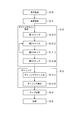
- FIG. 1 is a view showing a flowchart of the semiconductor wafer dicing method of the present embodiment.
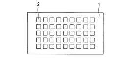
- FIG. 2 is an element layout diagram for explaining the semiconductor wafer dicing method of this embodiment.
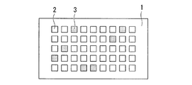
- FIG. 3 is an element layout diagram for explaining the semiconductor wafer dicing method of this embodiment.
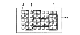
- FIG. 4 is an element layout diagram for explaining the semiconductor wafer dicing method of this embodiment.
- FIG. 5 is an element layout diagram for explaining the semiconductor wafer dicing method of this embodiment.
- FIG. 6 is an element layout diagram for explaining the semiconductor wafer dicing method of this embodiment.
- FIG. 7 is an element layout diagram for explaining the semiconductor wafer dicing method of this embodiment.
- 8A and 8B are diagrams for explaining a conventional dicing method of a semiconductor wafer.
- FIG. 8A shows a case of a large element size
- FIG. 8B shows a case of a small element size.
- the semiconductor wafer dicing method of this embodiment includes a step of forming a plurality of elements on the semiconductor wafer (element forming step), and a step of evaluating non-defective elements by evaluating the characteristics of the elements. (Decision determination step), a step (dicing line determination step) for determining a cutting line for cutting and separating the non-defective area on the semiconductor wafer on which the non-defective element is formed for each predetermined element, and along each cutting line And a step of cutting the semiconductor wafer (dicing step).
- an element formation step indicated by S-0 in FIG. 1 is performed.
- a plurality of chips (elements) 2 serving as a basic unit are formed on a semiconductor wafer 1 as shown in FIG.
- 9 ⁇ 5 chips will be described as an example.
- the semiconductor wafer 1 is not particularly limited, and examples thereof include a Si semiconductor substrate and a silicon carbide semiconductor substrate. In particular, when a silicon carbide semiconductor substrate in which many defects are likely to remain in the substrate and the epitaxial growth layer is used, the effect of the present invention becomes remarkable. Further, the size of the semiconductor wafer 1 is not particularly limited. For example, a semiconductor wafer having a size of 2 to 6 inches can be preferably used.
- the chip 2 is not particularly limited, and examples include a chip having a Schottky barrier diode, a vertical MOSFET, a lateral MOSFET, a PN diode, and the like. Further, the size and quantity of the chips 2 formed on the semiconductor wafer 1 are not particularly limited. For example, it is preferable to form about 2 to 9 elements of 1 to 10 mm square. In the present embodiment, the plurality of chips 2 formed on the semiconductor wafer 1 are connected by adjacent chips until dicing.
- a pass / fail judgment step indicated by S-1 in FIG. 1 is performed.
- a predetermined element characteristic evaluation is performed on all the chips 2 formed on the semiconductor wafer 1 to determine pass / fail.
- element characteristic evaluation is not specifically limited, Specifically, electrical characteristic evaluation can be illustrated.
- the non-defective chip 2 can be identified by marking the chip 3 determined to be defective as a result of the quality determination.
- an area on the semiconductor wafer 1 where a non-defective chip 2 other than the non-defective chip 3 is disposed is referred to as a non-defective area.
- the dicing line determination step includes a first step of determining a cutting line in which a predetermined number of chips can be arranged in the aggregate chip in which two or more chips are bonded to the non-defective area; A second step for determining a cutting line in which the next largest chip can be arranged from the non-defective area where the cutting line has not been determined, and a second step for gradually repeating the second step until a collective chip is formed by combining the two chips. 3 steps, and a fourth step of determining a cutting line for a single chip from a non-defective product area in which each cutting line is not determined.
- a cutting line in which the largest number of chips of a predetermined size can be arranged among the collective chips in which two or more chips are bonded to the non-defective area is determined.
- the aggregate chips of a predetermined size are coupled by 2 chips ⁇ 2 chips 2.
- a collective chip 4 a well-known technique can be used as means for arranging the largest number of collective chips 4 in the non-defective area. For example, image processing means, optimal cutting line calculation by a computer, and the like can be mentioned. In this way, the cutting line 4 a of the collective chip 4 is determined in the non-defective area on the semiconductor wafer 1.
- the second step shown in S-2-2 in FIG. 1 is performed.
- a cutting line on which the largest aggregate chip next to the aggregate chip 4 can be arranged is determined from the non-defective area where the cutting line 4a has not been determined.
- the non-defective product area in which the cutting line 4a is not determined refers to a good product area in which the collective chip 4 is not disposed as shown in FIG.
- the next largest aggregate chip after the aggregate chip 4 is an aggregate chip 5 in which two chips 2 are combined in a 1 ⁇ 2 configuration.
- the means for arranging the aggregate chips 5 in the non-defective area the same means as in the first step can be used. In this way, the cutting line 5a of the collective chip 5 is further determined in the non-defective area on the semiconductor wafer 1 where the cutting line 4a of the collective chip 4 is provided.
- the aggregate chip 5 is formed by combining two chips.
- the aggregate chip size may be determined in multiple stages.
- the second step can be repeated a plurality of times until a collective chip in which two chips are combined (S-2-3 in FIG. 1). As a result, more sized collective chips can be taken out from one semiconductor wafer 1 in stages.
- the fourth step shown in S-2-4 in FIG. 1 is performed.
- the cutting line 2a of the single chip 2 is determined from the non-defective area where the cutting lines 4a and 5a are not determined. That is, the fourth step is provided for taking out the non-defective chip 2 alone when a desired collective chip cannot be taken out from the non-defective area.
- the non-defective chip can be made from the non-defective area formed on the semiconductor wafer 1, so that the yield can be improved. As described above, as shown in FIG.
- the dicing line 6 for cutting and separating the non-defective area on the semiconductor wafer 1 on which the non-defective chip 2 is formed into chips 2, 4 and 5 of a predetermined size. decide.
- the dicing line 6 is a cutting line in which the cutting lines 2a, 4a and 5a are assembled.
- a dicing step indicated by S-3 in FIG. 1 is performed.
- the semiconductor wafer 1 is cut along the dicing line 6 including the cutting lines 2a, 4a, and 5a.
- a dicer capable of cutting the semiconductor wafer 1 into an arbitrary shape can be used.
- the cutting method of the semiconductor wafer 1 is not particularly limited, and examples thereof include a method using a laser beam and a method using a high-pressure water flow. More specifically, for example, a laser dicer manufactured by DISCO or a laser dicing system LDS200 manufactured by SYNOVA can be applied as a method using laser light.
- the dicing step includes a dicing execution step for cutting the semiconductor wafer 1 with the dicer after performing the dicing line input step (S-3-1 in FIG. 1) for inputting the dicing line 6 to the dicer (FIG. 1). S-3-2) is performed. Thereby, the non-defective area on the semiconductor wafer 1 can be simultaneously cut into a plurality of collective chips 2, 4 and 5 of a plurality of sizes.
- a chip classification step indicated by S-4 in FIG. 1 and a shipping step indicated by S-5 in FIG. 1 are performed.
- This chip classification step is a step of removing each defective chip 3 on the semiconductor wafer 1 and classifying each set chip 2, 4, 5 taken out by dicing for each set.
- the shipping step is a step for performing inspection, packing, and shipping work before shipping.
- the conventional semiconductor wafer dicing method for example, when it is desired to form a relatively large element having a current per one element (chip) of about 30 A, a chip of a desired size is formed on the entire surface of the semiconductor wafer, It was taken out by dicing. In such a case, the area occupied by one element is large, and even if a minute defect is included in the region on the semiconductor wafer, it becomes a defective product, and it is difficult to improve the yield.
- a relatively small element having a current per element of about 10 A is formed, even if a small defect is included in the region on the semiconductor wafer because the area occupied by one element is small. The influence on the yield is small (see FIGS. 8A and 8B).
- a relatively large element is formed in a region on a semiconductor wafer that does not include a minute defect, and a relatively small element is formed in a region that includes a minute defect.
- good elements having different sizes can be taken out without waste, and it is considered that productivity can be improved.
- the use of a method of grasping the position of a minute defect on a semiconductor wafer in advance and changing the product layout for each semiconductor wafer has a problem of increasing the cost.
- the basic minimum unit chip 2 is formed on the semiconductor wafer 1, and when the current per chip is 10A, for example, the non-defective product 2
- the collective chip connecting the individual pieces is used as a 20A element, and the collective chip connecting the three pieces is used as a 30A element.
- the cutting line 4a of the largest collective chip 4a is set, and then the cutting line of the gradually smaller collective chip is set, and the dicing line 6 is set.
- the basic minimum unit element is finally diced and one non-defective chip can be taken out from the non-defective area, productivity can be improved.
- the non-defective area on the semiconductor wafer 1 on which the non-defective chip 2 is formed is a collective chip in which a single element 2 or two or more elements are combined. It has the structure which determines the cutting lines 2a, 4a, and 5a for cutting and separating every 4 and 5.
- the non-defective area on the semiconductor wafer 1 can be simultaneously cut into a plurality of sized chips 2, 4 and 5, so that the non-defective area can be used as a chip (element) without waste. Therefore, a plurality of chips 2, 4, and 5 having different sizes can be simultaneously obtained from the semiconductor wafer 1 with a high yield.
- a semiconductor wafer cutting method that determines and cuts a semiconductor wafer along a cutting line. By this method, a plurality of elements of different sizes can be simultaneously obtained from the semiconductor wafer with a high yield.
Landscapes
- Dicing (AREA)
Abstract
半導体ウエーハ上に形成された素子の特性を評価して、良品の素子を識別するステップと、良品の素子が形成された半導体ウェーハ上の良品エリアを、所定の素子ごとに切断分離するための切断ラインを決定するステップと、各切断ラインに沿って半導体ウェーハを切断するステップと、を備えることを特徴とする半導体ウェーハのダイシング方法によって、半導体ウエーハから複数の異なるサイズの素子を同時に歩留まり良く取得することができる。
Description
本発明は、半導体ウェーハのダイシング方法に関するものである。
本発明は、2009年2月20日に、日本に出願された特願2009-038240号に基づき優先権を主張し、その内容をここに援用する。
本発明は、2009年2月20日に、日本に出願された特願2009-038240号に基づき優先権を主張し、その内容をここに援用する。
炭化珪素半導体は、シリコン半導体よりも絶縁破壊電圧が大きく、エネルギーバンドギャップが広く、また、熱伝導度が高いなど優れた特徴を有するので、発光素子、大電力パワーデバイス、耐高温素子、耐放射線素子、高周波素子等への応用が期待されている。
上記炭化珪素半導体を用いて素子(SiC半導体素子)を形成するためには、例えば、炭化珪素基板(SiC基板)上に半導体素子の活性領域としてエピタキシャル成長層を形成し、このエピタキシャル成長層の選択された領域で導電型やキャリア濃度を制御することが必要となる。そこで、不純物ドーパント原子を活性領域であるエピタキシャル成長層中に部分的に注入することによって、p型又はn型の各種不純物ドープ領域を形成し、トランジスタやダイオードなどの半導体素子を構成することが可能となる。
しかしながら、炭化珪素半導体には、炭化珪素基板中及びエピタキシャル成長層中に多くの欠陥が残存している。これらの欠陥は、素子特性を悪化させ、歩留まりを低下させる原因となるため、低減することが望まれるが、未だ十分なレベルに低減できていないのが実情である。
素子を分離する手段としては、ダイシングが用いられる。ダイシングは通常、特性の良否によるダイシング位置を考慮せずに、ダイサーの回転するブレードを用いて、ウェーハを格子状に切断する(例えば特許文献1)。また、特許文献2に記載のダイシング方法では、特性の良否によるダイシング位置を考慮せずに、複数のダイオードを連結したダイオードを形成している。
特性の良否を反映して半導体素子を切断分離するダイシング方法としては、例えば、特許文献3に記載のダイシング方法が知られている。具体的に特許文献3に記載のダイシング方法では、電気的特性試験結果に基づいて良品とされた素子を切断分離するのに必要な切断ラインを決定した後に、この切断ラインについて切断を行う構成を有している。このため、不必要な切断ラインに対する切断工程の省略が可能とされている。
上述したように、特許文献1のダイシング方法では、素子が形成された半導体ウェーハが素子のサイズでダイシングされるものである。このため、素子を不良にする欠陥密度(個/cm2)が同一である場合に、半導体ウェーハ上の占有面積が小さい素子を形成する場合と比較して、半導体ウェーハ上の占有面積が大きい素子を形成する場合に、基板等に残存する欠陥による歩留まり低下への影響が大きいという問題があった(図8(a)及び図8(b)参照)。特に、パワー半導体では、素子のサイズを大きくすることで大きな電流を流すことのできる素子が望まれているという事情があった。
本発明は、上記事情を鑑みてなされたもので、半導体ウェーハから複数の異なるサイズの素子を同時に歩留まりよく取得可能な半導体ウェーハのダイシング方法を提供することを目的とする。
本願発明者は、半導体ウェーハ上の素子の特性を評価後、良品の素子を必要数だけ繋げた集合素子を大電流素子とし、残ったものは小電流素子としてダイシングすることにより、一度に電流の異なる複数のサイズの素子を歩留まり良く得られることを見出して本願発明を完成させた。
すなわち、本発明は以下に関する。
(1) 複数の素子が形成された半導体ウェーハを、単独の素子又は2以上の素子が結合した集合素子ごとに切断分離する半導体ウェーハのダイシング方法であって、素子の特性を評価して、良品の素子を識別するステップと、良品の素子が形成された半導体ウェーハ上の良品エリアを、所定の素子ごとに切断分離するための切断ラインを決定するステップと、各切断ラインに沿って半導体ウェーハを切断するステップと、を備えることを特徴とする半導体ウェーハのダイシング方法。
(2) 良品の素子が形成された半導体ウェーハ上の良品エリアを、所定の素子ごとに切断分離するための切断ラインを決定するステップが、良品エリアに、2以上の素子が結合した集合素子の中で所定の大きさの素子を最も多く配置可能な切断ラインを決定する第1ステップと、切断ラインが決定されていない良品エリアから、所定の大きさのよりも小さい素子を最も多く配置可能な切断ラインを決定する第2ステップと、2つの素子が結合した集合素子となるまで前記第2ステップを漸次繰り返す第3ステップと、各切断ラインが決定されていない良品エリアから、単独の素子の切断ラインを決定する第4ステップと、を備えることを特徴とする前項(1)に記載の半導体ウェーハのダイシング方法。
(3) 前記単独の素子及び前記2以上の素子が結合した集合素子には、不良品の素子が含まれないことを特徴とする前項(1)又は(2)に記載の半導体ウェーハのダイシング方法。
(4) 各切断ラインに沿って半導体ウェーハを切断するステップが、レーザー光を用いることを特徴とする前項(1)乃至(3)のいずれか一項に記載の半導体ウェーハのダイシング方法。
(5) 各切断ラインに沿って半導体ウェーハを切断するステップが、高圧水流を用いることを特徴とする前項(1)乃至(3)のいずれか一項に記載の半導体ウェーハのダイシング方法。
(6) 前記半導体ウェーハが、炭化珪素半導体基板であることを特徴とする前項(1)乃至(5)のいずれか一項に記載の半導体ウェーハのダイシング方法。
(7) 前記素子が、ショットキーバリアダイオード、縦型MOSFET、横型MOSFET、PNダイオードのいずれかであることを特徴とする前項(1)乃至(6)のいずれか一項に記載の半導体ウェーハのダイシング方法。
(1) 複数の素子が形成された半導体ウェーハを、単独の素子又は2以上の素子が結合した集合素子ごとに切断分離する半導体ウェーハのダイシング方法であって、素子の特性を評価して、良品の素子を識別するステップと、良品の素子が形成された半導体ウェーハ上の良品エリアを、所定の素子ごとに切断分離するための切断ラインを決定するステップと、各切断ラインに沿って半導体ウェーハを切断するステップと、を備えることを特徴とする半導体ウェーハのダイシング方法。
(2) 良品の素子が形成された半導体ウェーハ上の良品エリアを、所定の素子ごとに切断分離するための切断ラインを決定するステップが、良品エリアに、2以上の素子が結合した集合素子の中で所定の大きさの素子を最も多く配置可能な切断ラインを決定する第1ステップと、切断ラインが決定されていない良品エリアから、所定の大きさのよりも小さい素子を最も多く配置可能な切断ラインを決定する第2ステップと、2つの素子が結合した集合素子となるまで前記第2ステップを漸次繰り返す第3ステップと、各切断ラインが決定されていない良品エリアから、単独の素子の切断ラインを決定する第4ステップと、を備えることを特徴とする前項(1)に記載の半導体ウェーハのダイシング方法。
(3) 前記単独の素子及び前記2以上の素子が結合した集合素子には、不良品の素子が含まれないことを特徴とする前項(1)又は(2)に記載の半導体ウェーハのダイシング方法。
(4) 各切断ラインに沿って半導体ウェーハを切断するステップが、レーザー光を用いることを特徴とする前項(1)乃至(3)のいずれか一項に記載の半導体ウェーハのダイシング方法。
(5) 各切断ラインに沿って半導体ウェーハを切断するステップが、高圧水流を用いることを特徴とする前項(1)乃至(3)のいずれか一項に記載の半導体ウェーハのダイシング方法。
(6) 前記半導体ウェーハが、炭化珪素半導体基板であることを特徴とする前項(1)乃至(5)のいずれか一項に記載の半導体ウェーハのダイシング方法。
(7) 前記素子が、ショットキーバリアダイオード、縦型MOSFET、横型MOSFET、PNダイオードのいずれかであることを特徴とする前項(1)乃至(6)のいずれか一項に記載の半導体ウェーハのダイシング方法。
本発明の半導体ウェーハのダイシング方法によれば、良品の素子が形成された半導体ウェーハ上の良品エリアを、単独の素子又は2以上の素子が結合した集合素子ごとに切断分離するための切断ラインを決定する構成を有している。これにより、半導体ウェーハ上の良品エリアを同時に複数のサイズの素子ごとに切断することができるため、良品エリアを無駄なく素子として活用することができる。したがって、半導体ウェーハから複数の異なるサイズの素子を同時に歩留まりよく取得することができる。
以下、本発明を適用した一実施形態である半導体ウェーハのダイシング方法について、図面を用いて詳細に説明する。なお、以下の説明で用いる図面は、特徴をわかりやすくするために、便宜上特徴となる部分を拡大して示している場合があり、各構成要素の寸法比率などが実際と同じであるとは限らない。
図1に示すように、本実施形態の半導体ウェーハのダイシング方法は、半導体ウェーハ上に複数の素子を形成するステップ(素子形成ステップ)と、素子の特性を評価して良品の素子を識別するステップ(良否判定ステップ)と、良品の素子が形成された半導体ウェーハ上の良品エリアを所定の素子ごとに切断分離するための切断ラインを決定するステップ(ダイシングライン決定ステップ)と、各切断ラインに沿って半導体ウェーハを切断するステップ(ダイシングステップ)とから概略構成されている。
(素子形成ステップ)
先ず、図1中のS-0に示す素子形成ステップを行う。この素子形成ステップでは、図2に示すように、半導体ウェーハ1上に、基礎となる最小単位のチップ(素子)2を複数形成する。なお、本実施形態では、9×5個のチップを例にして説明する。
先ず、図1中のS-0に示す素子形成ステップを行う。この素子形成ステップでは、図2に示すように、半導体ウェーハ1上に、基礎となる最小単位のチップ(素子)2を複数形成する。なお、本実施形態では、9×5個のチップを例にして説明する。
半導体ウェーハ1は、特に限定されるものではないが、Si半導体基板や炭化珪素半導体基板を例示することができる。特に、基板中及びエピタキシャル成長層中に多くの欠陥が残存しやすい炭化珪素半導体基板を用いた場合に、本発明の効果が顕著となる。また、半導体ウェーハ1のサイズは、特に限定されるものではないが、例えば、2~6インチのサイズの半導体ウェーハを好適に用いることができる。
チップ2は、特に限定されるものではないが、例えば、ショットキーバリアダイオード、縦型MOSFET、横型MOSFET、PNダイオード等を有するものを例示することができる。また、半導体ウェーハ1上に形成するチップ2のサイズ及び数量は、特に限定されるものではないが、例えば、1~10mm角の素子を2~9個程度形成することが好ましい。なお、本実施形態では、半導体ウェーハ1上に形成された複数のチップ2は、ダイシングされるまでは隣接するチップ同士で接続されている。
(良否判定ステップ)
次に、図1中のS-1に示す良否判定ステップを行う。この良否判定ステップでは、半導体ウェーハ1上に形成したチップ2の全てに対して、所定の素子特性評価を行って良否を判定する。素子特性評価は、特に限定されるものではないが、具体的には、電気的特性評価を例示することができる。また、図3に示すように、良否判定の結果、不良品と判定されたチップ3にマーキング等を施すことにより、良品のチップ2を識別可能とする。なお、以下の説明において、半導体ウェーハ1上の領域であって、不良品と判定されたチップ3が配置された以外の、良品のチップ2が配置された領域を良品エリアという。
次に、図1中のS-1に示す良否判定ステップを行う。この良否判定ステップでは、半導体ウェーハ1上に形成したチップ2の全てに対して、所定の素子特性評価を行って良否を判定する。素子特性評価は、特に限定されるものではないが、具体的には、電気的特性評価を例示することができる。また、図3に示すように、良否判定の結果、不良品と判定されたチップ3にマーキング等を施すことにより、良品のチップ2を識別可能とする。なお、以下の説明において、半導体ウェーハ1上の領域であって、不良品と判定されたチップ3が配置された以外の、良品のチップ2が配置された領域を良品エリアという。
(ダイシングライン決定ステップ)
次に、図1中のS-2に示すダイシングライン決定ステップを行う。より具体的には、このダイシングライン決定ステップは、良品エリアに2以上のチップが結合した集合チップの中で所定の大きさのチップを最も多く配置可能な切断ラインを決定する第1ステップと、切断ラインが決定されていない良品エリアから、次に大きなチップを最も多く配置可能な切断ラインを決定する第2ステップと、2つのチップが結合した集合チップとなるまで前記第2ステップを漸次繰り返す第3ステップと、各切断ラインが決定されていない良品エリアから、単独のチップの切断ラインを決定する第4ステップと、を備えている。
次に、図1中のS-2に示すダイシングライン決定ステップを行う。より具体的には、このダイシングライン決定ステップは、良品エリアに2以上のチップが結合した集合チップの中で所定の大きさのチップを最も多く配置可能な切断ラインを決定する第1ステップと、切断ラインが決定されていない良品エリアから、次に大きなチップを最も多く配置可能な切断ラインを決定する第2ステップと、2つのチップが結合した集合チップとなるまで前記第2ステップを漸次繰り返す第3ステップと、各切断ラインが決定されていない良品エリアから、単独のチップの切断ラインを決定する第4ステップと、を備えている。
(第1ステップ)
先ず、図1中のS-2-1に示す第1ステップを行う。この第1ステップでは、良品エリアに2以上のチップが結合した集合チップの中で所定の大きさのチップを最も多く配置可能な切断ラインを決定する。ここで、図4に示すように、本実施形態では、2以上のチップ2が結合した集合チップの中で所定の大きさの集合チップを、4つのチップ2が2個×2個で結合した集合チップ4とする。また、良品エリアに集合チップ4を最も多く配置する手段としては、公知の技術を用いることができる。例えば、画像処理手段、コンピュータによる最適切断ライン計算等が挙げられる。このようにして、半導体ウェーハ1上の良品エリアに集合チップ4の切断ライン4aを決定する。
先ず、図1中のS-2-1に示す第1ステップを行う。この第1ステップでは、良品エリアに2以上のチップが結合した集合チップの中で所定の大きさのチップを最も多く配置可能な切断ラインを決定する。ここで、図4に示すように、本実施形態では、2以上のチップ2が結合した集合チップの中で所定の大きさの集合チップを、4つのチップ2が2個×2個で結合した集合チップ4とする。また、良品エリアに集合チップ4を最も多く配置する手段としては、公知の技術を用いることができる。例えば、画像処理手段、コンピュータによる最適切断ライン計算等が挙げられる。このようにして、半導体ウェーハ1上の良品エリアに集合チップ4の切断ライン4aを決定する。
(第2ステップ)
次に、図1中のS-2-2に示す第2ステップを行う。この第2ステップでは、切断ライン4aが決定されていない良品エリアから、集合チップ4の次に大きな集合チップを最も多く配置可能な切断ラインを決定する。ここで、切断ライン4aが決定されていない良品エリアとは、図5に示すように、集合チップ4が配置されていない良品エリアをいう。
また、本実施形態では、集合チップ4の次に大きな集合チップは、2つのチップ2が1個×2個で結合した集合チップ5とする。さらに、良品エリアに集合チップ5を最も多く配置する手段としては、上記第1ステップと同じ手段を用いることができる。このようにして、集合チップ4の切断ライン4aが設けられた半導体ウェーハ1上の良品エリアに、さらに集合チップ5の切断ライン5aを決定する。
次に、図1中のS-2-2に示す第2ステップを行う。この第2ステップでは、切断ライン4aが決定されていない良品エリアから、集合チップ4の次に大きな集合チップを最も多く配置可能な切断ラインを決定する。ここで、切断ライン4aが決定されていない良品エリアとは、図5に示すように、集合チップ4が配置されていない良品エリアをいう。
また、本実施形態では、集合チップ4の次に大きな集合チップは、2つのチップ2が1個×2個で結合した集合チップ5とする。さらに、良品エリアに集合チップ5を最も多く配置する手段としては、上記第1ステップと同じ手段を用いることができる。このようにして、集合チップ4の切断ライン4aが設けられた半導体ウェーハ1上の良品エリアに、さらに集合チップ5の切断ライン5aを決定する。
(第3ステップ)
本実施形態では、第1ステップから第2ステップを実施したところで2つのチップが結合した集合チップ5となるが、これよりも多段階的に集合チップのサイズを決定してもよい。かかる場合には、第3ステップとして、2つのチップが結合した集合チップとなるまで前記第2ステップを複数回繰り返すことができる(図1中のS-2-3)。これにより、1枚の半導体ウェーハ1から、より多くのサイズの集合チップを段階的に取り出すことができる。
本実施形態では、第1ステップから第2ステップを実施したところで2つのチップが結合した集合チップ5となるが、これよりも多段階的に集合チップのサイズを決定してもよい。かかる場合には、第3ステップとして、2つのチップが結合した集合チップとなるまで前記第2ステップを複数回繰り返すことができる(図1中のS-2-3)。これにより、1枚の半導体ウェーハ1から、より多くのサイズの集合チップを段階的に取り出すことができる。
(第4ステップ)
次に、図1中のS-2-4に示す第4ステップを行う。この第4ステップでは、図6に示すように、各切断ライン4a及び5aが決定されていない良品エリアから、単独のチップ2の切断ライン2aを決定する。すなわち、この第4ステップでは、良品エリアから所望の集合チップが取り出せない場合において、良品のチップ2を単独で取り出すために設けられている。この第4ステップにより、半導体ウェーハ1上に形成された良品エリアから良品チップを余すところなく製品とすることができるため、歩留まりを向上させることができる。以上のようにして、図7に示すように、良品のチップ2が形成された半導体ウェーハ1上の良品エリアを所定のサイズのチップ2,4,5ごとに切断分離するためのダイシングライン6を決定する。なお、ダイシングライン6は、各切断ライン2a,4a,5aの集合した切断ラインである。
次に、図1中のS-2-4に示す第4ステップを行う。この第4ステップでは、図6に示すように、各切断ライン4a及び5aが決定されていない良品エリアから、単独のチップ2の切断ライン2aを決定する。すなわち、この第4ステップでは、良品エリアから所望の集合チップが取り出せない場合において、良品のチップ2を単独で取り出すために設けられている。この第4ステップにより、半導体ウェーハ1上に形成された良品エリアから良品チップを余すところなく製品とすることができるため、歩留まりを向上させることができる。以上のようにして、図7に示すように、良品のチップ2が形成された半導体ウェーハ1上の良品エリアを所定のサイズのチップ2,4,5ごとに切断分離するためのダイシングライン6を決定する。なお、ダイシングライン6は、各切断ライン2a,4a,5aの集合した切断ラインである。
(ダイシングステップ)
次に、図1中のS-3に示すダイシングステップを行う。このダイシングステップでは、各切断ライン2a,4a,5aからなるダイシングライン6に沿って半導体ウェーハ1を切断する。本実施形態のダイシングステップには、半導体ウェーハ1を任意の形状に切断できるダイサーを用いることができる。また、半導体ウェーハ1の切断方法は、特に限定されるものではないが、レーザー光を用いる方法や高圧水流を用いる方法を例示することができる。より具体的には、レーザー光を用いる方法としては、例えば、DISCO社のレーザダイサーやSYNOVA社のレーザー・ダイシング・システムLDS200等を適用することができる。
次に、図1中のS-3に示すダイシングステップを行う。このダイシングステップでは、各切断ライン2a,4a,5aからなるダイシングライン6に沿って半導体ウェーハ1を切断する。本実施形態のダイシングステップには、半導体ウェーハ1を任意の形状に切断できるダイサーを用いることができる。また、半導体ウェーハ1の切断方法は、特に限定されるものではないが、レーザー光を用いる方法や高圧水流を用いる方法を例示することができる。より具体的には、レーザー光を用いる方法としては、例えば、DISCO社のレーザダイサーやSYNOVA社のレーザー・ダイシング・システムLDS200等を適用することができる。
具体的にダイシングステップは、ダイサーにダイシングライン6を入力するダイシングライン入力ステップ(図1中のS-3-1)を行った後、ダイサーによって半導体ウェーハ1を切断するダイシング実行ステップ(図1中のS-3-2)を行う。これにより、半導体ウェーハ1上の良品エリアを同時に複数のサイズの集合チップ2,4,5ごとに切断することができる。
なお、本実施形態の半導体ウェーハのダイシング方法の後工程としては、図1中のS-4に示すチップ分類ステップと、図1中のS-5に示す出荷ステップを行う。このチップ分類ステップは、半導体ウェーハ1上の不良品のチップ3を取り除くと共にダイシングによって取り出した各集合チップ2,4,5を集合ごとに分類するステップである。また、出荷ステップは、出荷前の検査、梱包、出荷作業を行うステップである。
ところで、従来の半導体ウェーハのダイシング方法によれば、例えば1素子(チップ)あたりの電流が30A程度の比較的大きな素子を形成したい場合、半導体ウェーハ上の全面に所望のサイズのチップを形成し、ダイシングを行うことで取り出していた。かかる場合に、1素子が占有する面積は大きく、半導体ウェーハ上の領域に微小な欠陥が含まれていた場合であっても不良品となるため、歩留まりの改善が困難であった。一方、1素子あたりの電流が10A程度の比較的小さな素子を形成した場合は、1素子が占有する面積が小さいために半導体ウェーハ上の領域に微小な欠陥が含まれていた場合であっても歩留まりへの影響が少ない(図8(a)及び図8(b)参照)。
ここで、従来の半導体ウェーハのダイシング方法において、微小な欠陥が含まれていない半導体ウェーハ上の領域には比較的大きな素子を形成し、微小な欠陥が含まれている領域に比較的小さな素子を形成すると、サイズの異なる良品の素子を無駄なく取り出すことができるため、生産性を向上することができるとも考えられる。しかしながら、例えば半導体ウェーハ上の微小な欠陥の位置を事前に把握して、半導体ウェーハごとに製品レイアウトを変更する方法の採用は、コストを上昇させてしまうという問題があった。
これに対して、本実施形態の半導体ウェーハのダイシング方法では、半導体ウェーハ1上に基本となる最小単位のチップ2を形成し、例えば、この1チップあたりの電流を10Aとしたときに、良品2個を繋げた集合チップを20A素子、3個を繋げた集合チップを30A素子として用いる。そして、半導体ウェーハ1上の良品のチップ2が形成された良品エリアから、先ず最も大きい集合チップ4aの切断ライン4aを設定し、それから漸次小さい集合チップの切断ラインを設定して、ダイシングライン6を決定している。このため、不良品のチップ3を含むことなく、大きなチップから優先的に効率よく取得することができる。また、最後に基本となる最小単位の素子をダイシングして、良品エリアから1つ残らず良品チップを取り出すことができるため、生産性を向上することができる。
以上説明したように、本実施形態の半導体ウェーハのダイシング方法によれば、良品のチップ2が形成された半導体ウェーハ1上の良品エリアを、単独の素子2又は2以上の素子が結合した集合チップ4,5ごとに切断分離するための切断ライン2a,4a,5aを決定する構成を有している。これにより、半導体ウェーハ1上の良品エリアを同時に複数のサイズのチップ2,4,5ごとに切断することができるため、良品エリアを無駄なくチップ(素子)として活用することができる。したがって、半導体ウェーハ1から複数の異なるサイズのチップ2,4,5を同時に歩留まりよく取得することができる。
多数の素子が形成された半導体ウエーハの素子の特性を評価して良品の素子を識別し、良品からなる単独の素子または2以上の素子が結合した集合素子ごとに切断分離するための切断ラインを決定し、切断ラインに沿って半導体のウエーハを切断する半導体ウエーハの切断方法であって、この方法によって、半導体ウエーハから複数の異なるサイズの素子を同時に歩留まり良く取得することができる。
1・・・半導体ウェーハ
2・・・チップ(素子)
2a・・・切断ライン
3・・・不良品と判定されたチップ
4,5・・・集合チップ
4a,5a・・・切断ライン
6・・・ダイシングライン
2・・・チップ(素子)
2a・・・切断ライン
3・・・不良品と判定されたチップ
4,5・・・集合チップ
4a,5a・・・切断ライン
6・・・ダイシングライン
Claims (7)
- 複数の素子が形成された半導体ウェーハを、単独の素子又は2以上の素子が結合した集合素子ごとに切断分離する半導体ウェーハのダイシング方法であって、
素子の特性を評価して、良品の素子を識別するステップと、
良品の素子が形成された半導体ウェーハ上の良品エリアを、所定の素子ごとに切断分離するための切断ラインを決定するステップと、
各切断ラインに沿って半導体ウェーハを切断するステップと、を備えることを特徴とする半導体ウェーハのダイシング方法。 - 良品の素子が形成された半導体ウェーハ上の良品エリアを、所定の素子ごとに切断分離するための切断ラインを決定するステップが、
良品エリアに、2以上の素子が結合した集合素子の中で所定の大きさの素子を最も多く配置可能な切断ラインを決定する第1ステップと、
切断ラインが決定されていない良品エリアから、所定の大きさのよりも小さい素子を最も多く配置可能な切断ラインを決定する第2ステップと、
2つの素子が結合した集合素子となるまで前記第2ステップを漸次繰り返す第3ステップと、
各切断ラインが決定されていない良品エリアから、単独の素子の切断ラインを決定する第4ステップと、を備えることを特徴とする請求項1に記載の半導体ウェーハのダイシング方法。 - 前記単独の素子及び前記2以上の素子が結合した集合素子には、不良品の素子が含まれないことを特徴とする請求項1又は2に記載の半導体ウェーハのダイシング方法。
- 各切断ラインに沿って半導体ウェーハを切断するステップが、レーザー光を用いることを特徴とする請求項1乃至3のいずれか一項に記載の半導体ウェーハのダイシング方法。
- 各切断ラインに沿って半導体ウェーハを切断するステップが、高圧水流を用いることを特徴とする請求項1乃至3のいずれか一項に記載の半導体ウェーハのダイシング方法。
- 前記半導体ウェーハが、炭化珪素半導体基板であることを特徴とする請求項1乃至5のいずれか一項に記載の半導体ウェーハのダイシング方法。
- 前記素子が、ショットキーバリアダイオード、縦型MOSFET、横型MOSFET、PNダイオードのいずれかであることを特徴とする請求項1乃至6のいずれか一項に記載の半導体ウェーハのダイシング方法。
Applications Claiming Priority (2)
| Application Number | Priority Date | Filing Date | Title |
|---|---|---|---|
| JP2009038240A JP2010192837A (ja) | 2009-02-20 | 2009-02-20 | 半導体ウェーハのダイシング方法 |
| JP2009-038240 | 2009-02-20 |
Publications (1)
| Publication Number | Publication Date |
|---|---|
| WO2010095355A1 true WO2010095355A1 (ja) | 2010-08-26 |
Family
ID=42633647
Family Applications (1)
| Application Number | Title | Priority Date | Filing Date |
|---|---|---|---|
| PCT/JP2010/000343 Ceased WO2010095355A1 (ja) | 2009-02-20 | 2010-01-21 | 半導体ウェーハのダイシング方法 |
Country Status (2)
| Country | Link |
|---|---|
| JP (1) | JP2010192837A (ja) |
| WO (1) | WO2010095355A1 (ja) |
Cited By (1)
| Publication number | Priority date | Publication date | Assignee | Title |
|---|---|---|---|---|
| CN111696983A (zh) * | 2020-06-24 | 2020-09-22 | 悦虎晶芯电路(苏州)股份有限公司 | 多芯片水平封装的芯片模组、晶圆结构和加工方法 |
Families Citing this family (4)
| Publication number | Priority date | Publication date | Assignee | Title |
|---|---|---|---|---|
| US9093356B2 (en) | 2010-12-28 | 2015-07-28 | Nichia Corporation | Semiconductor light emitting element |
| EP2660882B1 (en) | 2010-12-28 | 2018-10-03 | Nichia Corporation | Semiconductor light-emitting device |
| JP6645520B2 (ja) | 2016-02-01 | 2020-02-14 | 株式会社ニコン | 撮像素子の製造方法、撮像素子、および撮像装置 |
| JP2022085738A (ja) * | 2020-11-27 | 2022-06-08 | パナソニックIpマネジメント株式会社 | チップの製造方法 |
Citations (4)
| Publication number | Priority date | Publication date | Assignee | Title |
|---|---|---|---|---|
| JPH0878617A (ja) * | 1994-08-22 | 1996-03-22 | Internatl Business Mach Corp <Ibm> | 電子モジュールおよびその製造方法 |
| JPH09199450A (ja) * | 1996-01-22 | 1997-07-31 | Oki Electric Ind Co Ltd | ウエハ上の半導体素子ダイシング方法及び装置 |
| JPH11330256A (ja) * | 1998-05-19 | 1999-11-30 | Tif:Kk | 半導体装置およびその製造方法 |
| JP2004327708A (ja) * | 2003-04-24 | 2004-11-18 | Sanyo Electric Co Ltd | 半導体装置およびその製造方法 |
-
2009
- 2009-02-20 JP JP2009038240A patent/JP2010192837A/ja active Pending
-
2010
- 2010-01-21 WO PCT/JP2010/000343 patent/WO2010095355A1/ja not_active Ceased
Patent Citations (4)
| Publication number | Priority date | Publication date | Assignee | Title |
|---|---|---|---|---|
| JPH0878617A (ja) * | 1994-08-22 | 1996-03-22 | Internatl Business Mach Corp <Ibm> | 電子モジュールおよびその製造方法 |
| JPH09199450A (ja) * | 1996-01-22 | 1997-07-31 | Oki Electric Ind Co Ltd | ウエハ上の半導体素子ダイシング方法及び装置 |
| JPH11330256A (ja) * | 1998-05-19 | 1999-11-30 | Tif:Kk | 半導体装置およびその製造方法 |
| JP2004327708A (ja) * | 2003-04-24 | 2004-11-18 | Sanyo Electric Co Ltd | 半導体装置およびその製造方法 |
Cited By (2)
| Publication number | Priority date | Publication date | Assignee | Title |
|---|---|---|---|---|
| CN111696983A (zh) * | 2020-06-24 | 2020-09-22 | 悦虎晶芯电路(苏州)股份有限公司 | 多芯片水平封装的芯片模组、晶圆结构和加工方法 |
| CN111696983B (zh) * | 2020-06-24 | 2024-03-15 | 悦虎晶芯电路(苏州)股份有限公司 | 多芯片水平封装的芯片模组、晶圆结构和加工方法 |
Also Published As
| Publication number | Publication date |
|---|---|
| JP2010192837A (ja) | 2010-09-02 |
Similar Documents
| Publication | Publication Date | Title |
|---|---|---|
| KR101766562B1 (ko) | 탄화규소 반도체 장치의 제조 방법 | |
| Marcon et al. | Manufacturing challenges of GaN-on-Si HEMTs in a 200 mm CMOS fab | |
| JP6729757B2 (ja) | 炭化珪素半導体基板、炭化珪素半導体基板の製造方法、半導体装置および半導体装置の製造方法 | |
| WO2010095355A1 (ja) | 半導体ウェーハのダイシング方法 | |
| TW200849670A (en) | Process for producing compound semiconductor device and compound semiconductor device | |
| WO2018150861A1 (ja) | 炭化ケイ素積層基板およびその製造方法 | |
| TW200903869A (en) | Semiconductor light-emitting device and method for manufacturing the same | |
| CN111326612A (zh) | 混搭不同等级led芯片的布局方法及显示装置 | |
| JP2017055010A (ja) | 半導体装置 | |
| JP2020004856A (ja) | 半導体装置の製造方法 | |
| JP7209513B2 (ja) | 半導体チップの製造方法および半導体ウェハ | |
| US8987867B2 (en) | Wafer and method of manufacturing the same | |
| JP5599675B2 (ja) | Ledデバイスチップの製造方法 | |
| JP6883745B2 (ja) | 半導体装置およびその製造方法 | |
| JP2009200382A (ja) | 半導体発光素子の製造方法 | |
| US5766973A (en) | Method for manufacturing a semiconductor arrangement by introducing crystal disorder structures and varying diffusion rates | |
| JP6956064B2 (ja) | 半導体装置、基板、及び、半導体装置の製造方法。 | |
| CN103579439B (zh) | 发光二极管管芯及其制造方法 | |
| US11424322B2 (en) | Semiconductor device and method of manufacturing the same | |
| JP2018113288A (ja) | 炭化珪素半導体装置の製造方法 | |
| CN102825668A (zh) | 一种含介电层的半导体原件的切割方法 | |
| US20110095399A1 (en) | Method For Manufacturing Semiconductor Chips From A Wafer | |
| US8900925B2 (en) | Method for manufacturing a diode, and a diode | |
| JP2017041616A (ja) | 化合物半導体素子 | |
| JP5989422B2 (ja) | 半導体装置の製造方法 |
Legal Events
| Date | Code | Title | Description |
|---|---|---|---|
| 121 | Ep: the epo has been informed by wipo that ep was designated in this application |
Ref document number: 10743488 Country of ref document: EP Kind code of ref document: A1 |
|
| NENP | Non-entry into the national phase |
Ref country code: DE |
|
| 122 | Ep: pct application non-entry in european phase |
Ref document number: 10743488 Country of ref document: EP Kind code of ref document: A1 |