WO2010064560A1 - 接続フィルム、並びに、接合体及びその製造方法 - Google Patents
接続フィルム、並びに、接合体及びその製造方法 Download PDFInfo
- Publication number
- WO2010064560A1 WO2010064560A1 PCT/JP2009/069798 JP2009069798W WO2010064560A1 WO 2010064560 A1 WO2010064560 A1 WO 2010064560A1 JP 2009069798 W JP2009069798 W JP 2009069798W WO 2010064560 A1 WO2010064560 A1 WO 2010064560A1
- Authority
- WO
- WIPO (PCT)
- Prior art keywords
- general formula
- film according
- following structural
- group
- connection film
- Prior art date
- Legal status (The legal status is an assumption and is not a legal conclusion. Google has not performed a legal analysis and makes no representation as to the accuracy of the status listed.)
- Ceased
Links
Images




Classifications
-
- C—CHEMISTRY; METALLURGY
- C09—DYES; PAINTS; POLISHES; NATURAL RESINS; ADHESIVES; COMPOSITIONS NOT OTHERWISE PROVIDED FOR; APPLICATIONS OF MATERIALS NOT OTHERWISE PROVIDED FOR
- C09J—ADHESIVES; NON-MECHANICAL ASPECTS OF ADHESIVE PROCESSES IN GENERAL; ADHESIVE PROCESSES NOT PROVIDED FOR ELSEWHERE; USE OF MATERIALS AS ADHESIVES
- C09J5/00—Adhesive processes in general; Adhesive processes not provided for elsewhere, e.g. relating to primers
- C09J5/06—Adhesive processes in general; Adhesive processes not provided for elsewhere, e.g. relating to primers involving heating of the applied adhesive
-
- C—CHEMISTRY; METALLURGY
- C09—DYES; PAINTS; POLISHES; NATURAL RESINS; ADHESIVES; COMPOSITIONS NOT OTHERWISE PROVIDED FOR; APPLICATIONS OF MATERIALS NOT OTHERWISE PROVIDED FOR
- C09J—ADHESIVES; NON-MECHANICAL ASPECTS OF ADHESIVE PROCESSES IN GENERAL; ADHESIVE PROCESSES NOT PROVIDED FOR ELSEWHERE; USE OF MATERIALS AS ADHESIVES
- C09J7/00—Adhesives in the form of films or foils
- C09J7/30—Adhesives in the form of films or foils characterised by the adhesive composition
-
- C—CHEMISTRY; METALLURGY
- C08—ORGANIC MACROMOLECULAR COMPOUNDS; THEIR PREPARATION OR CHEMICAL WORKING-UP; COMPOSITIONS BASED THEREON
- C08L—COMPOSITIONS OF MACROMOLECULAR COMPOUNDS
- C08L33/00—Compositions of homopolymers or copolymers of compounds having one or more unsaturated aliphatic radicals, each having only one carbon-to-carbon double bond, and only one being terminated by only one carboxyl radical, or of salts, anhydrides, esters, amides, imides or nitriles thereof; Compositions of derivatives of such polymers
- C08L33/24—Homopolymers or copolymers of amides or imides
-
- C—CHEMISTRY; METALLURGY
- C08—ORGANIC MACROMOLECULAR COMPOUNDS; THEIR PREPARATION OR CHEMICAL WORKING-UP; COMPOSITIONS BASED THEREON
- C08L—COMPOSITIONS OF MACROMOLECULAR COMPOUNDS
- C08L35/00—Compositions of homopolymers or copolymers of compounds having one or more unsaturated aliphatic radicals, each having only one carbon-to-carbon double bond, and at least one being terminated by a carboxyl radical, and containing at least one other carboxyl radical in the molecule, or of salts, anhydrides, esters, amides, imides or nitriles thereof; Compositions of derivatives of such polymers
- C08L35/06—Copolymers with vinyl aromatic monomers
-
- C—CHEMISTRY; METALLURGY
- C09—DYES; PAINTS; POLISHES; NATURAL RESINS; ADHESIVES; COMPOSITIONS NOT OTHERWISE PROVIDED FOR; APPLICATIONS OF MATERIALS NOT OTHERWISE PROVIDED FOR
- C09J—ADHESIVES; NON-MECHANICAL ASPECTS OF ADHESIVE PROCESSES IN GENERAL; ADHESIVE PROCESSES NOT PROVIDED FOR ELSEWHERE; USE OF MATERIALS AS ADHESIVES
- C09J9/00—Adhesives characterised by their physical nature or the effects produced, e.g. glue sticks
- C09J9/02—Electrically-conducting adhesives
-
- H—ELECTRICITY
- H05—ELECTRIC TECHNIQUES NOT OTHERWISE PROVIDED FOR
- H05K—PRINTED CIRCUITS; CASINGS OR CONSTRUCTIONAL DETAILS OF ELECTRIC APPARATUS; MANUFACTURE OF ASSEMBLAGES OF ELECTRICAL COMPONENTS
- H05K1/00—Printed circuits
- H05K1/02—Details
- H05K1/0266—Marks, test patterns or identification means
- H05K1/0269—Marks, test patterns or identification means for visual or optical inspection
-
- H—ELECTRICITY
- H05—ELECTRIC TECHNIQUES NOT OTHERWISE PROVIDED FOR
- H05K—PRINTED CIRCUITS; CASINGS OR CONSTRUCTIONAL DETAILS OF ELECTRIC APPARATUS; MANUFACTURE OF ASSEMBLAGES OF ELECTRICAL COMPONENTS
- H05K3/00—Apparatus or processes for manufacturing printed circuits
- H05K3/30—Assembling printed circuits with electric components, e.g. with resistors
- H05K3/32—Assembling printed circuits with electric components, e.g. with resistors electrically connecting electric components or wires to printed circuits
- H05K3/321—Assembling printed circuits with electric components, e.g. with resistors electrically connecting electric components or wires to printed circuits by conductive adhesives
- H05K3/323—Assembling printed circuits with electric components, e.g. with resistors electrically connecting electric components or wires to printed circuits by conductive adhesives by applying an anisotropic conductive adhesive layer over an array of pads
-
- C—CHEMISTRY; METALLURGY
- C08—ORGANIC MACROMOLECULAR COMPOUNDS; THEIR PREPARATION OR CHEMICAL WORKING-UP; COMPOSITIONS BASED THEREON
- C08K—Use of inorganic or non-macromolecular organic substances as compounding ingredients
- C08K5/00—Use of organic ingredients
- C08K5/0008—Organic ingredients according to more than one of the "one dot" groups of C08K5/01 - C08K5/59
-
- C—CHEMISTRY; METALLURGY
- C09—DYES; PAINTS; POLISHES; NATURAL RESINS; ADHESIVES; COMPOSITIONS NOT OTHERWISE PROVIDED FOR; APPLICATIONS OF MATERIALS NOT OTHERWISE PROVIDED FOR
- C09J—ADHESIVES; NON-MECHANICAL ASPECTS OF ADHESIVE PROCESSES IN GENERAL; ADHESIVE PROCESSES NOT PROVIDED FOR ELSEWHERE; USE OF MATERIALS AS ADHESIVES
- C09J2301/00—Additional features of adhesives in the form of films or foils
- C09J2301/40—Additional features of adhesives in the form of films or foils characterized by the presence of essential components
- C09J2301/416—Additional features of adhesives in the form of films or foils characterized by the presence of essential components use of irradiation
-
- H—ELECTRICITY
- H05—ELECTRIC TECHNIQUES NOT OTHERWISE PROVIDED FOR
- H05K—PRINTED CIRCUITS; CASINGS OR CONSTRUCTIONAL DETAILS OF ELECTRIC APPARATUS; MANUFACTURE OF ASSEMBLAGES OF ELECTRICAL COMPONENTS
- H05K2203/00—Indexing scheme relating to apparatus or processes for manufacturing printed circuits covered by H05K3/00
- H05K2203/16—Inspection; Monitoring; Aligning
- H05K2203/161—Using chemical substances, e.g. colored or fluorescent, for facilitating optical or visual inspection
-
- H—ELECTRICITY
- H05—ELECTRIC TECHNIQUES NOT OTHERWISE PROVIDED FOR
- H05K—PRINTED CIRCUITS; CASINGS OR CONSTRUCTIONAL DETAILS OF ELECTRIC APPARATUS; MANUFACTURE OF ASSEMBLAGES OF ELECTRICAL COMPONENTS
- H05K2203/00—Indexing scheme relating to apparatus or processes for manufacturing printed circuits covered by H05K3/00
- H05K2203/16—Inspection; Monitoring; Aligning
- H05K2203/163—Monitoring a manufacturing process
-
- H—ELECTRICITY
- H10—SEMICONDUCTOR DEVICES; ELECTRIC SOLID-STATE DEVICES NOT OTHERWISE PROVIDED FOR
- H10W—GENERIC PACKAGES, INTERCONNECTIONS, CONNECTORS OR OTHER CONSTRUCTIONAL DETAILS OF DEVICES COVERED BY CLASS H10
- H10W72/00—Interconnections or connectors in packages
- H10W72/071—Connecting or disconnecting
- H10W72/073—Connecting or disconnecting of die-attach connectors
-
- H—ELECTRICITY
- H10—SEMICONDUCTOR DEVICES; ELECTRIC SOLID-STATE DEVICES NOT OTHERWISE PROVIDED FOR
- H10W—GENERIC PACKAGES, INTERCONNECTIONS, CONNECTORS OR OTHER CONSTRUCTIONAL DETAILS OF DEVICES COVERED BY CLASS H10
- H10W74/00—Encapsulations, e.g. protective coatings
- H10W74/10—Encapsulations, e.g. protective coatings characterised by their shape or disposition
- H10W74/15—Encapsulations, e.g. protective coatings characterised by their shape or disposition on active surfaces of flip-chip devices, e.g. underfills
-
- H—ELECTRICITY
- H10—SEMICONDUCTOR DEVICES; ELECTRIC SOLID-STATE DEVICES NOT OTHERWISE PROVIDED FOR
- H10W—GENERIC PACKAGES, INTERCONNECTIONS, CONNECTORS OR OTHER CONSTRUCTIONAL DETAILS OF DEVICES COVERED BY CLASS H10
- H10W90/00—Package configurations
- H10W90/701—Package configurations characterised by the relative positions of pads or connectors relative to package parts
- H10W90/721—Package configurations characterised by the relative positions of pads or connectors relative to package parts of bump connectors
- H10W90/724—Package configurations characterised by the relative positions of pads or connectors relative to package parts of bump connectors between a chip and a stacked insulating package substrate, interposer or RDL
-
- H—ELECTRICITY
- H10—SEMICONDUCTOR DEVICES; ELECTRIC SOLID-STATE DEVICES NOT OTHERWISE PROVIDED FOR
- H10W—GENERIC PACKAGES, INTERCONNECTIONS, CONNECTORS OR OTHER CONSTRUCTIONAL DETAILS OF DEVICES COVERED BY CLASS H10
- H10W90/00—Package configurations
- H10W90/701—Package configurations characterised by the relative positions of pads or connectors relative to package parts
- H10W90/731—Package configurations characterised by the relative positions of pads or connectors relative to package parts of die-attach connectors
- H10W90/734—Package configurations characterised by the relative positions of pads or connectors relative to package parts of die-attach connectors between a chip and a stacked insulating package substrate, interposer or RDL
Definitions
- the present invention relates to a connection film, a joined body, and a manufacturing method thereof, and more particularly, a connection film capable of electrically and mechanically connecting circuit members such as an IC chip and a liquid crystal panel (LCD panel) in a liquid crystal display (LCD).
- a connection film capable of electrically and mechanically connecting circuit members such as an IC chip and a liquid crystal panel (LCD panel) in a liquid crystal display (LCD).
- the present invention relates to a joined body including a connection film and a manufacturing method thereof.
- a tape-like connection material for example, anisotropic conductive film (ACF) in which a curable resin in which conductive particles are dispersed is applied to a release film.
- ACF anisotropic conductive film
- This anisotropic conductive film (connection film) is used when, for example, a terminal of a flexible printed circuit board (FPC) or an IC chip is connected to an ITO (Indium Tin Oxide) electrode formed on the glass substrate of the LCD panel. First, it is used when various terminals are bonded and electrically connected.
- connection film includes one in which conductive particles are dispersed in an epoxy resin, and one in which conductive particles are dispersed in an acrylic resin. These connection films (organic resin layers) are cured by heating to connect the substrates (circuit members).
- connection state of the substrate (circuit member) is usually grasped by measuring the curing degree of the connection film (organic resin layer) using an analyzer such as IR or DSC.
- an analyzer such as IR or DSC.
- connection film organic resin layer
- imidazole-based curing agent an imidazole-based curing agent
- the red color of the connection film has been used as a standard for the completion of curing by utilizing the characteristic that the connection film turns red (for example, Patent Document 1).
- connection film using the imidazole curing agent instead of the connection film using the imidazole curing agent, the acrylic connection film using the radical curing agent is actively used. It is supposed to be. Therefore, in acrylic connection films using radical curing agents, the development of technology that can visually estimate the degree of cure of the connection film (organic resin layer) is similar to connection films using imidazole curing agents. In particular, there is a strong demand from device manufacturers.
- connection films for example, Patent Documents 2 and 3 in which a coloring component develops color as curing progresses are disclosed.
- the coloring components are colored after being pressed onto the substrate, and it is difficult to distinguish the corroded part in appearance inspection (such as inspection of the number of conductive particles and crushing state) and corrosion tests. There was a problem of becoming.
- these connecting films have a problem that the recognition sensor cannot be recognized when the adhesive film is set in the temporary attachment device because the coloring component is not colored before the pressure bonding.
- Patent Document 4 an adhesive (for example, Patent Document 4) containing a decoloring component (a salt of a cyanine dye and an organic boron compound) that is colored at the time of application and becomes colorless by light irradiation after application is disclosed.
- a decoloring component a salt of a cyanine dye and an organic boron compound
- Patent Document 4 is not a decoloring reaction caused by the reaction of the curing agent as in the present invention. Therefore, if the adhesive of Patent Document 4 is transferred to the connection film as it is, it will not be decolored to express the degree of cure, and the decolored part will not necessarily be a part where curing has progressed. This is also a cause (Patent Document 4 is an invention for identifying the application state by decoloring to the last).
- JP-A-4-145180 JP-A-11-307154 JP 2007-91798 A Japanese Patent Laid-Open No. 5-132655
- the present invention makes it a subject to solve the said conventional problems and to achieve the following objectives. That is, the present invention can grasp the connection state with the substrate visually, and can easily determine the corroded portion in the appearance inspection and the corrosion test after being crimped to the substrate, and An object of the present invention is to provide a joined body joined by the connection film and a method for producing the joined body.
- connection film comprising an organic resin layer containing a decolorizable dye, a curable organic resin, a curing agent, and conductive particles.
- the connection film according to ⁇ 1> since the pigment contained in the organic resin layer has a decoloring property, the connection state with the substrate can be grasped visually, and after being pressure-bonded to the substrate. Appearance inspection and corrosion test can be easily performed.
- the connection film according to the above ⁇ 1> is colored even before being bonded to the substrate, it is possible to facilitate reading of the recognition sensor when setting the temporary attachment device.
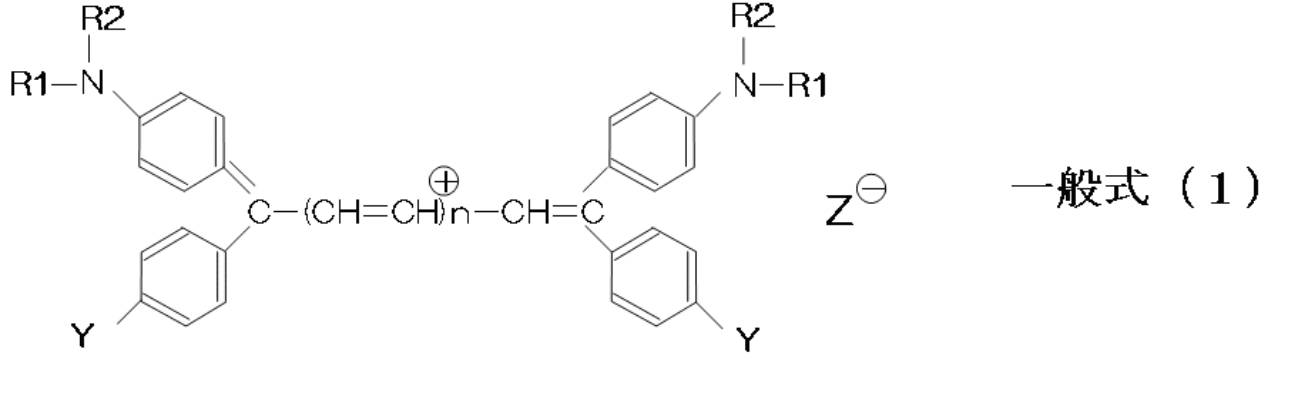
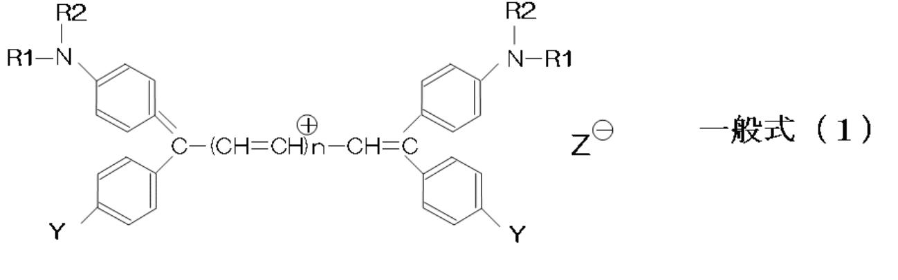
- connection film according to ⁇ 1> wherein the decolorizable dye includes a compound represented by the following general formula (1).
- R1 and R2 are each a hydrogen atom, an alkyl group, or an aryl group
- Y is a hydrogen atom, a halogen atom, an alkyl group, an aryl group, a dimethylamino group, or a diethylamino group.
- a methoxy group, or an ethoxy group, Z ⁇ is a counter anion
- n is 0-3.
- R1 and R2 are each a hydrogen atom, an alkyl group, or an aryl group
- Y is a hydrogen atom, a halogen atom, an alkyl group, an aryl group, a dimethylamino group, or a diethylamino group.
- Z ⁇ is a counter anion
- n is an integer of 0 to 3.
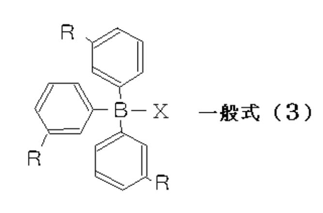
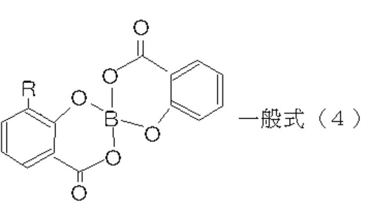
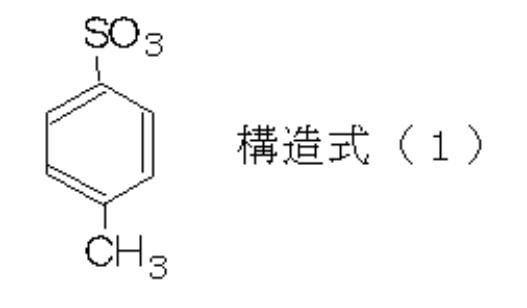
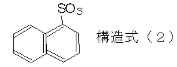
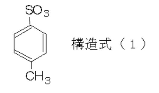
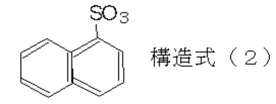
- ⁇ 4> Z is represented by ClO 4 , BF 4 , CF 3 SO 3 , a compound represented by the following general formula (3), a compound represented by the following general formula (4), and the following structural formula (1).
- connection film according to any one of ⁇ 2> to ⁇ 3>, which is any one of a compound represented by the following structural formula (2):
- R is either a hydrogen atom or a fluorine atom
- X is an alkyl group.
- R is either a hydrogen atom or a fluorine atom.
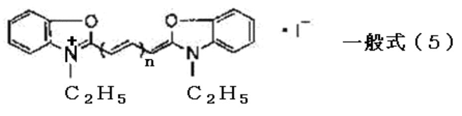
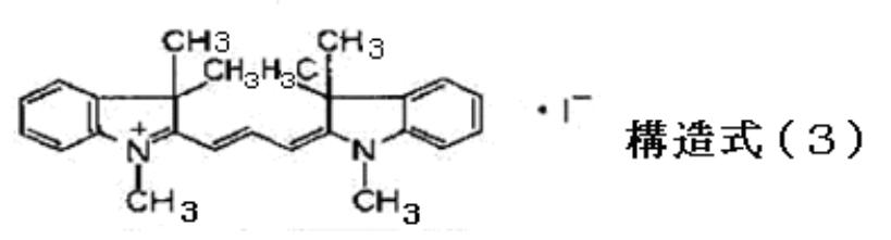
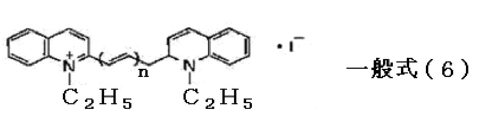
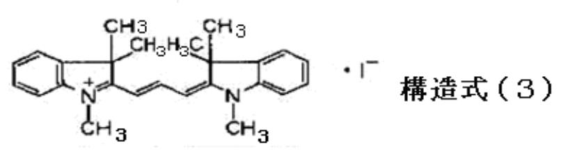
- ⁇ 5> A compound having a decolorizable dye represented by the following general formula (5), a compound represented by the following general formula (6), a compound represented by the following structural formula (3), and the following structural formula (4) ) And at least one selected from the compounds represented by the following general formula (7).
- n is an integer of 1 to 3.
- n is an integer of 1 to 3.
- n is an integer of 1 to 3.
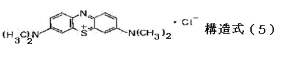
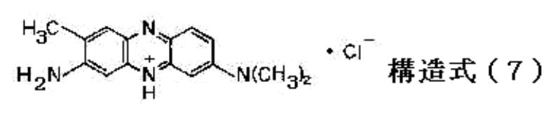
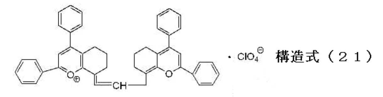
- ⁇ 6> The connection film according to ⁇ 1>, wherein the decolorizable dye includes at least one selected from compounds represented by the following structural formulas (5) to (7).
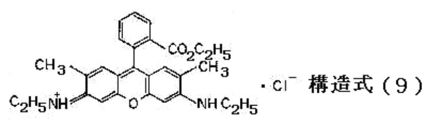
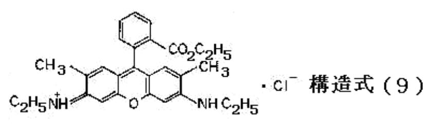
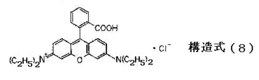
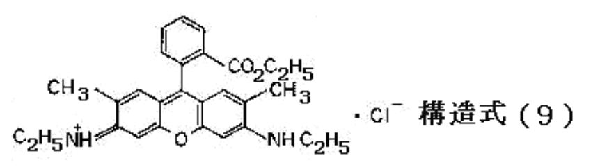
- ⁇ 7> The connection film according to ⁇ 1>, wherein the decolorizable dye includes at least one selected from compounds represented by the following structural formulas (8) to (9).
- ⁇ 8> The connection film according to ⁇ 1>, wherein the decolorizable dye includes at least one selected from compounds represented by the following structural formulas (10) to (11).
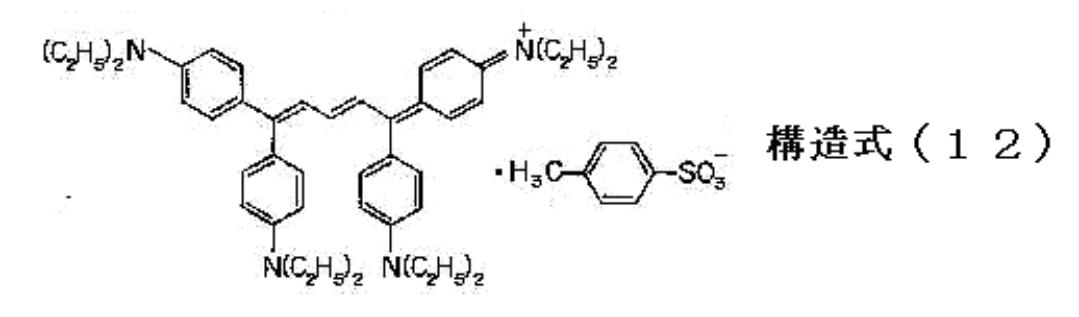
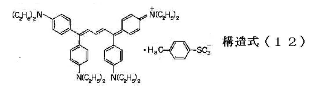
- ⁇ 9> The connection film according to ⁇ 1>, wherein the decolorizable dye includes a compound represented by the following structural formula (12).
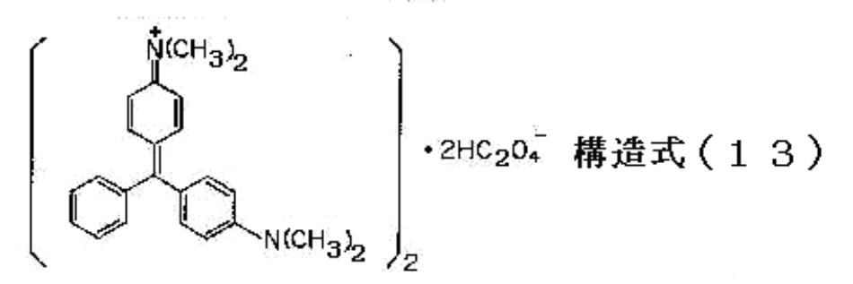
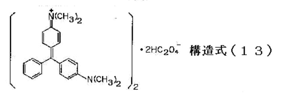
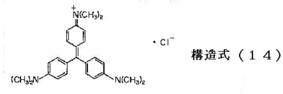
- connection film according to ⁇ 1> wherein the decolorizable dye includes at least one selected from compounds represented by the following structural formulas (13) to (15).
- the decolorizable dye includes at least one selected from compounds represented by the following structural formulas (16) to (17).
- the decolorizable dye includes at least one selected from compounds represented by the following structural formulas (18) to (19).
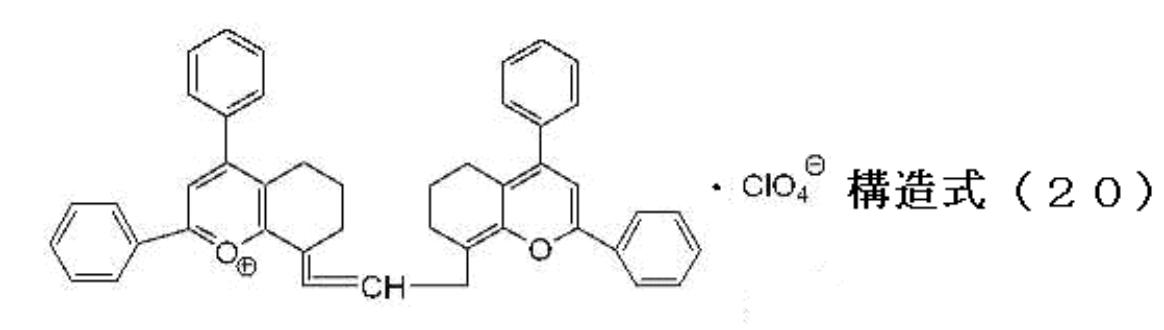
- the decolorizable dye includes at least one selected from compounds represented by the following structural formulas (20) to (21).
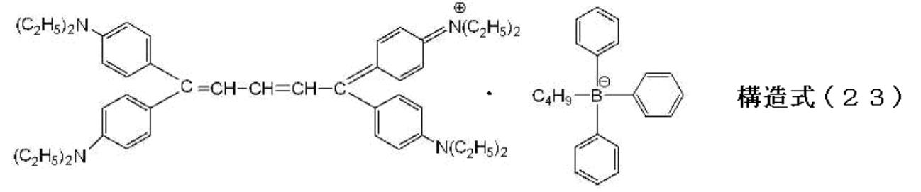
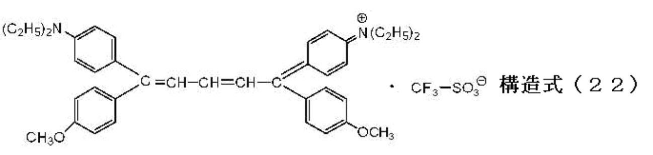
- connection film according to ⁇ 1> wherein the decolorizable dye includes at least one selected from compounds represented by the following structural formulas (22) to (23).
- the curable organic resin is an acrylic resin, and the curing agent is a radical curing agent.
- the curable organic resin is an epoxy resin, and the curing agent is a cationic curing agent.
- ⁇ 17> including a connection step of bonding the first and second substrates by heating or irradiation with light through the connection film according to any one of ⁇ 1> to ⁇ 16>, wherein the connection step In the method for producing a joined body, the decolorizable dye is decolored when the curing reaction of the organic resin layer is completed.
- the connection step In the method for producing a joined body, the decolorizable dye is decolored when the curing reaction of the organic resin layer is completed.
- ⁇ 18> A joined body produced by the method for producing a joined body according to ⁇ 17>.
- connection film capable of easily distinguishing a corroded portion in a property test, a joined body joined by the connection film, and a method for manufacturing the same.
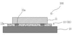
- FIG. 1 is a schematic explanatory view showing a joined body of the present invention.
- FIG. 2 is a schematic explanatory view showing the connection film of the present invention.
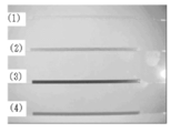
- FIG. 3 is a photograph showing a state of the connection film before pressure bonding.
- (1) is a radical bonding material R1
- (2) is a radical bonding material A2
- (3) is a radical bonding material R2
- (4) is a radical bonding material R3.
- FIG. 4 is a photograph showing the result of decoloring confirmation after mounting of Comparative Example 1.
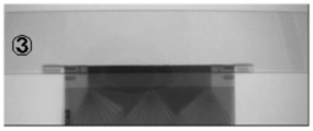
- FIG. 5 is a photograph showing the result of decoloring confirmation after mounting of Example 2.
- FIG. 6 is a photograph showing the result of decoloring confirmation after mounting of Comparative Example 3.
- FIG. 7 is a photograph showing the result of decoloring confirmation after mounting of Comparative Example 4.
- the joined body of the present invention includes a first substrate (first circuit member), a second substrate (second circuit member), and a connection film, and further appropriately selected as necessary. It has other members.
- the joined body 100 includes a first substrate (first circuit member) 10, a second substrate (second circuit member) 11, and a connection film 12 (an organic resin described later). Layer 21). Terminals 11a on the second substrate (second circuit member) 11, conductive particles 12a dispersed in the connection film 12, and terminals (not shown) on the first substrate (first circuit member) 10. Is electrically connected, the first substrate (first circuit member) 10 and the second substrate (second circuit member) 11 are electrically connected.
- substrate (1st circuit member) There is no restriction
- connection film has an organic resin layer, and further has other layers appropriately selected as necessary.
- the organic resin layer is a conductive particle-containing organic resin layer containing conductive particles.
- the connection film 12 includes a release layer (separator) 20 and a conductive particle-containing organic resin layer 21 formed on the release layer (separator) 20.
- Organic resin layer is disposed between the first substrate (first circuit member) and the second substrate (second circuit member), and has a decolorizable dye, a curable organic resin, a curing agent, and If it contains electroconductive particle, there will be no restriction
- the organic resin layer may be a single layer or a plurality of layers. When the organic resin layer is a plurality of layers, the decolorizable dye, the curable organic resin, the curing agent, and the conductive particles may be included in the same layer or in different layers. . Further, the bonding material for forming the organic resin layer may be a paste or a film.
- Discolorable Dye examples include those that decolorize after the connection film is pressure-bonded (not only those that change colorlessly, but also have the same color (yellow to light yellow) as the color of the conductive fine particles described later (light yellow). As long as it is discolored), it can be appropriately selected according to the purpose.
- These decolorizable dyes may be included alone or in combination of two or more. Furthermore, a plurality of cation parts (parts other than the counter anion) of these decolorizable dyes may be contained.
- the preferable content of the decolorizable dye is 0.5 to 3.0 parts by mass with respect to 100 parts by mass of the whole binder (including curable resin and other resins) contained in the organic resin layer.
- the amount is preferably 3.0 parts by mass to 6.0 parts by mass with respect to 100 parts by mass of the curable resin contained in the organic resin layer.
- the compound represented by the following structural formula (3) is red before the connection film is pressure-bonded, but becomes colorless after pressure-bonding the connection film, and the compound represented by the following structural formula (5) is Although it is blue before the connection film is pressure-bonded, it turns pale yellow after the connection film is pressure-bonded, and the compound represented by the following structural formula (7) is purple before the connection film is pressure-bonded.
- the compound represented by the following structural formula (8) turns red after the film is pressure-bonded, and is red before the connection film is pressure-bonded, but becomes colorless after the connection film is pressure-bonded, and is represented by the following structural formula (9).
- the compound represented is red before the connection film is pressure-bonded, but becomes colorless after the connection film is pressure-bonded, and the compound represented by the following structural formula (10) is It is yellow before pressure bonding, but becomes light yellow after pressure bonding the connection film, and the compound represented by the following structural formula (11) is yellow before pressure bonding the connection film.
- the compound represented by the following structural formula (12) is blue before the connection film is pressure-bonded, but becomes colorless after the connection film is pressure-bonded, and is represented by the following structural formula (13).
- the compound represented is blue before the connection film is pressure-bonded, but becomes colorless after the connection film is pressure-bonded, and the compound represented by the following structural formula (14) is blue before the connection film is pressure-bonded. However, it becomes light yellow after the connection film is pressure-bonded.
- R1 and R2 are each a hydrogen atom, an alkyl group, or an aryl group
- Y is a hydrogen atom, a halogen atom, an alkyl group, an aryl group, a dimethylamino group, or a diethylamino group.
- a methoxy group, or an ethoxy group, Z ⁇ is a counter anion, and n is 0-3.
- Examples of the counter anion (Z ⁇ ) include halogen ions, perchlorate ions, p-toluenesulfonate ions, trifluoromethanesulfonate ions, trifluoroacetate ions, tetraalkylboron anions, tetrafluoroboron ions, oxalate ions, and the like.
- any structure may be used as long as it has a high stability.
- the reaction rate, storage stability, etc. can be increased, and can be used properly depending on the application.
- the counter anion Z - Specific examples of Z in the, ClO 4, BF 4, CF 3 SO 3, a compound represented by the following general formula (3), a compound represented by the following general formula (4), the following structure Examples thereof include a compound represented by the formula (1) and a compound represented by the following structural formula (2).
- R is either a hydrogen atom or a fluorine atom
- X is an alkyl group
- R is either a hydrogen atom or a fluorine atom.
- R1 and R2 are each a hydrogen atom, an alkyl group, or an aryl group
- Y is a hydrogen atom, a halogen atom, an alkyl group, an aryl group, a dimethylamino group, or a diethylamino group.
- a methoxy group, and an ethoxy group, Z ⁇ is a counter anion, and n is an integer of 0 to 3.
- the counter anion (Z ⁇ ) is the same as the counter anion in the general formula (1).
- n is an integer of 1 to 3.
- n is an integer of 1 to 3.
- n is an integer of 1 to 3.
- a light stabilizer may be added to the decolorizable dye.
- the light stabilizer is not particularly limited and may be appropriately selected depending on the intended purpose. Examples thereof include benzotriazole light stabilizers and hindered amine light stabilizers. By adding the light stabilizer, discoloration before use can be suppressed.
- the decolorization reaction due to the cation reaction is considered to be due to the reaction represented by the following reaction formula (2). Moreover, in the decoloring reaction by a cation reaction, it is thought that the decoloring reaction by the said radical reaction has also occurred simultaneously.
- Curable organic resin >>>
- a thermosetting organic resin is preferable and an acrylic resin, an epoxy resin, etc. are more preferable.
- Acrylic resin is not particularly limited and may be appropriately selected depending on the intended purpose.
- acrylic resins such as cartons and urethane acrylates. These may be used individually by 1 type and may use 2 or more types together. Moreover, what made the
- Epoxy resin >>>>>
- fever such as bisphenol A type epoxy resin, bisphenol F type epoxy resin, novolac type epoxy resin, and those modified epoxy resins
- a curable epoxy resin is mentioned. These may be used individually by 1 type and may use 2 or more types together.
- the curing agent is not particularly limited and may be appropriately selected depending on the purpose. However, when the curable organic resin is an acrylic resin, a radical curing agent is preferable, and when the curable organic resin is an epoxy resin. Cationic curing agents are preferred.
- Radical curing agent >>>>>
- curing agent there is no restriction
- ⁇ cationic curing agent >>>>>
- a sulfonium salt, onium salt, etc. can be mentioned, Among these, an aromatic sulfonium salt is preferable.
- the conductive particles are not particularly limited, and those used in conventional anisotropic conductive adhesives (connection films) can be used.
- metal particles or metal-coated resins having a particle diameter of 1 to 50 ⁇ m. Particles can be used.
- the metal particles include nickel, cobalt, copper and the like. In order to prevent such surface oxidation, particles whose surfaces are coated with gold or palladium may be used. Furthermore, you may use the surface which gave the metal film or the insulating film with organic substance.
- the metal-coated resin particles include true spherical particles plated with one or more of nickel, cobalt, copper and the like. Similarly, particles whose outermost surface is coated with gold or palladium may be used. Furthermore, you may use the surface which gave the metal film or the insulating film with organic substance.
- a peeling layer can be mentioned.
- the shape, structure, size, thickness, material (material), etc. of the release layer are not particularly limited and can be appropriately selected according to the purpose.
- a transparent release PET (polyethylene terephthalate) sheet coated with a release agent such as silicone is preferable.
- a PTFE (polytetrafluoroethylene) sheet may be used.
- the manufacturing method of the joined body of the present invention includes at least a joining step and further includes other steps appropriately selected as necessary.
- the joining step is a step of joining the first and second substrates by heating or irradiation with light through the connection film of the present invention.
- the heating is determined by the total amount of heat.
- the heating is performed at a heating temperature of 120 ° C. to 220 ° C.
- the light irradiation is performed by a UV irradiation apparatus such as a mercury lamp or a metal halide lamp.
- the pressure bonding differs depending on the type of the second substrate.
- the second substrate is FPC or TAB (Tape Automated Bonding)
- the pressure is 2 MPa to 6 MPa
- the second substrate is an IC chip
- the pressure is 30 MPa or more. It is performed at 150 MPa for 3 seconds to 10 seconds, respectively. Bonding may be performed using ultrasonic waves.
- a part shows a mass part.
- radical bonding material R1 60 parts of a phenoxy resin (product name: YP50, manufactured by Tohto Kasei Co., Ltd.), 35 parts of a radical polymerizable resin (product name: EB-600, manufactured by Daicel Cytec Co., Ltd.) as a curable resin, and a silane coupling agent (product name: KBM) -503, manufactured by Shin-Etsu Chemical Co., Ltd.) and 3 parts of a reaction initiator as a radical curing agent (Product name: Perhexa C, 10 hours half-life temperature 90.7 ° C., manufactured by NOF Corporation)
- This radical bonding material R1 was light yellow which is the color of the conductive particles (see (1) in FIG.
- radical bonding material R2 (Production of radical bonding material R2) To the radical bonding material R1, a quinone dye (CI Solvent Blue 35: AMMONIUM, ETHYL (4- (p- (ETHYL (m-SULFOFENZYL) AMINO) -alpha- (o-SULFOPHENYL) BENZYLIDENE) -2,5- A radical bonding material R2 containing 1 part of CYCLOHEXADIEN-1-YLIDENE) (m-SULFOBENZYL)-, HYDROXIDE, manufactured by Hodogaya Chemical Co., Ltd. was obtained. The color of the radical bonding material R2 was blue (see (3) in FIG. 3).
- radical bonding material R3 (Preparation of radical bonding material R3) To the radical bonding material R1, triphenylmethane dye (C.I Solvent Red 18: AMMONIUM, (6- (DIETHYLAMINO) -9- (2,4-DISULFOPHENYL) -3H-XANTHEN-3-YLIDENE) DIETHYL-, HYDROXIDE Radical bonding material R3 containing 1 part of Hodogaya Chemical Co., Ltd.) was obtained. The color of the radical bonding material R3 was red. (See (4) in FIG. 3).
- triphenylmethane dye C.I Solvent Red 18: AMMONIUM, (6- (DIETHYLAMINO) -9- (2,4-DISULFOPHENYL) -3H-XANTHEN-3-YLIDENE) DIETHYL-, HYDROXIDE Radical bonding material R3 containing 1 part of Hodogaya Chemical Co., Ltd.
- cation bonding material C1 60 parts of phenoxy resin (product name: YP50, manufactured by Toto Kasei Co., Ltd.), 35 parts of epoxy resin (product name: EP-828, manufactured by Japan Epoxy Resin Co., Ltd.) as a curable resin, and silane coupling agent (product name: KBM-403) , Manufactured by Shin-Etsu Chemical Co., Ltd.) and an adhesive composed of 3 parts of a reaction initiator (product name: SI-80L, manufactured by Sanshin Chemical Co., Ltd.) as a cationic curing agent.
- phenoxy resin product name: YP50, manufactured by Toto Kasei Co., Ltd.
- epoxy resin product name: EP-828, manufactured by Japan Epoxy Resin Co., Ltd.
- silane coupling agent product name: KBM-403
- Conductive particles (product name: AUL704) , Sekisui Chemical Co., Ltd.) was dispersed to a particle density of 10,000 particles / mm 2 to obtain a cationic bonding material C1 having a thickness of 15 ⁇ m.
- the cation bonding material C1 was light yellow, which is the color of the conductive particles.
- Radical bonding materials A1 to A10 in which R1, R2, Y, n, and Z each include one part each of dyes P1 to P10 of the following general formula (1) having the structure shown in Table 1 are obtained in the radical bonding material R1. It was. All of these radical bonding materials A1 to A10 were blue.
- Radical bonding material A2 (bonding material using P2 (1,1,5,5-tetrakis [4- (diethylamino) phenyl] -1,4-pentadiene-3-ylium-p-toluenesulfonate) as a dye)
- the photograph of (2) in FIG. 3 is shown.
- radical bonding material A11 In the production of the radical bonding material A1, instead of using perhexa C (10-hour half-life temperature 90.7 ° C., manufactured by NOF Corporation) as a reaction initiator, perocta ND (10-hour half-life temperature 40.7 ° C., NOF Corporation) A radical bonding material A11 was obtained in the same manner as in the preparation of the radical bonding material A1 except that the product was used.
- radical bonding material A12 In the production of the radical bonding material A1, instead of using perhexa C (10-hour half-life temperature 90.7 ° C., manufactured by NOF Corporation) as a reaction initiator, perhexine 25B (10-hour half-life temperature 128.4 ° C., NOF Corporation) A radical bonding material A12 was obtained in the same manner as in the preparation of the radical bonding material A1, except that the product was used.
- Radical bonding materials A13 to A17 were obtained, in which the radical bonding material R1 further contained one part each of the dyes P11 to P15 of the following structural formulas (7) to (9), (12), and (13).
- Example 1 Preparation of joined body
- COF substrate (Sony Chemical & Information Device Co., Ltd. evaluation substrate, 50 ⁇ m P, Sn plated 8 ⁇ m thick Cu, 38 ⁇ m thick S'perflex substrate) and ITO coating glass (Sony Chemical & Information Device Co., Ltd. evaluation)
- base material for use an entire surface ITO coat, and a glass thickness of 0.7 mm.
- a radical bonding material A1 slit to a width of 1.5 mm is laminated on ITO coated glass, and a COF substrate is temporarily fixed thereon, and then a buffer material (100 ⁇ m thick Teflon ( Using a registered trademark)), bonding was performed under a bonding condition of 190 ° C.-3 MPa-10 seconds to obtain a bonded body AJ1.
- a buffer material 100 ⁇ m thick Teflon ( Using a registered trademark)
- Example 2 In Example 1, instead of using the radical bonding material A1, a bonded body was produced in the same manner as in Example 1 except that the radical bonding material A2 was used to obtain a bonded body AJ2. Moreover, the decoloring confirmation after mounting (refer FIG. 5), the connection resistance measurement of a joined body, and the adhesive strength measurement of the joined body were performed similarly to Example 1. FIG. The results are shown in Table 2.
- Example 3 In Example 1, instead of using the radical bonding material A1, a bonded body was produced in the same manner as in Example 1 except that the radical bonding material A3 was used to obtain a bonded body AJ3. Further, in the same manner as in Example 1, decoloration confirmation after mounting, connection resistance measurement of the joined body, and adhesive strength measurement of the joined body were performed. The results are shown in Table 2.
- Example 4 In Example 1, instead of using the radical bonding material A1, a bonded body was produced in the same manner as in Example 1 except that the radical bonding material A4 was used to obtain a bonded body AJ4. Further, in the same manner as in Example 1, decoloration confirmation after mounting, connection resistance measurement of the joined body, and adhesive strength measurement of the joined body were performed. The results are shown in Table 2.
- Example 5 In Example 1, instead of using the radical bonding material A1, a bonded body was produced in the same manner as in Example 1 except that the radical bonding material A5 was used to obtain a bonded body AJ5. Further, in the same manner as in Example 1, decoloration confirmation after mounting, connection resistance measurement of the joined body, and adhesive strength measurement of the joined body were performed. The results are shown in Table 2.
- Example 6 In Example 1, instead of using the radical bonding material A1, a bonded body was produced in the same manner as in Example 1 except that the radical bonding material A6 was used to obtain a bonded body AJ6. Further, in the same manner as in Example 1, decoloration confirmation after mounting, connection resistance measurement of the joined body, and adhesive strength measurement of the joined body were performed. The results are shown in Table 2.
- Example 7 In Example 1, instead of using the radical bonding material A1, a bonded body was produced in the same manner as in Example 1 except that the radical bonding material A7 was used to obtain a bonded body AJ7. Further, in the same manner as in Example 1, decoloration confirmation after mounting, connection resistance measurement of the joined body, and adhesive strength measurement of the joined body were performed. The results are shown in Table 2.
- Example 8 In Example 1, instead of using the radical bonding material A1, a bonded body was produced in the same manner as in Example 1 except that the radical bonding material A8 was used to obtain a bonded body AJ8. Further, in the same manner as in Example 1, decoloration confirmation after mounting, connection resistance measurement of the joined body, and adhesive strength measurement of the joined body were performed. The results are shown in Table 2.
- Example 9 In Example 1, instead of using the radical bonding material A1, a bonded body was manufactured in the same manner as in Example 1 except that the radical bonding material A9 was used to obtain a bonded body AJ9. Further, in the same manner as in Example 1, decoloration confirmation after mounting, connection resistance measurement of the joined body, and adhesive strength measurement of the joined body were performed. The results are shown in Table 2.
- Example 10 In Example 1, instead of using the radical bonding material A1, a bonded body was produced in the same manner as in Example 1 except that the radical bonding material A10 was used to obtain a bonded body AJ10. Further, in the same manner as in Example 1, decoloration confirmation after mounting, connection resistance measurement of the joined body, and adhesive strength measurement of the joined body were performed. The results are shown in Table 2.
- Example 11 In Example 1, instead of using the radical bonding material A1, a bonded body was manufactured in the same manner as in Example 1 except that the radical bonding material A11 was used to obtain a bonded body AJ11. Further, in the same manner as in Example 1, decoloration confirmation after mounting, connection resistance measurement of the joined body, and adhesive strength measurement of the joined body were performed. The results are shown in Table 2.
- Example 12 In Example 1, instead of using the radical bonding material A1, a bonded body was produced in the same manner as in Example 1 except that the radical bonding material A12 was used to obtain a bonded body AJ12. Further, in the same manner as in Example 1, decoloration confirmation after mounting, connection resistance measurement of the joined body, and adhesive strength measurement of the joined body were performed. The results are shown in Table 2.
- Comparative Example 1 In Comparative Example 1, a joined body was produced in the same manner as in Example 1 except that the radical joining material R1 was used instead of the radical joining material A1, and a joined body RJ1 was obtained. Further, in the same manner as in Example 1, decoloration confirmation after mounting, connection resistance measurement of the joined body, and adhesive strength measurement of the joined body were performed. The results are shown in Table 2.
- Example 13 In Example 1, instead of using the radical bonding material A1, a bonded body was produced in the same manner as in Example 1 except that the radical bonding material A13 was used to obtain a bonded body AJ13. Further, in the same manner as in Example 1, decoloration confirmation after mounting, connection resistance measurement of the joined body, and adhesive strength measurement of the joined body were performed. The results are shown in Table 3.
- Example 14 In Example 1, instead of using the radical bonding material A1, a bonded body was produced in the same manner as in Example 1 except that the radical bonding material A14 was used to obtain a bonded body AJ14. Further, in the same manner as in Example 1, decoloration confirmation after mounting, connection resistance measurement of the joined body, and adhesive strength measurement of the joined body were performed. The results are shown in Table 3.
- Example 15 In Example 1, instead of using the radical bonding material A1, a bonded body was manufactured in the same manner as in Example 1 except that the radical bonding material A15 was used to obtain a bonded body AJ15. Further, in the same manner as in Example 1, decoloration confirmation after mounting, connection resistance measurement of the joined body, and adhesive strength measurement of the joined body were performed. The results are shown in Table 3.
- Example 16 In Example 1, instead of using the radical bonding material A1, a bonded body was produced in the same manner as in Example 1 except that the radical bonding material A16 was used to obtain a bonded body AJ16. Further, in the same manner as in Example 1, decoloration confirmation after mounting, connection resistance measurement of the joined body, and adhesive strength measurement of the joined body were performed. The results are shown in Table 3.
- Example 17 In Example 1, instead of using the radical bonding material A1, a bonded body was produced in the same manner as in Example 1 except that the radical bonding material A17 was used to obtain a bonded body AJ17. Further, in the same manner as in Example 1, decoloration confirmation after mounting, connection resistance measurement of the joined body, and adhesive strength measurement of the joined body were performed. The results are shown in Table 3.
- Example 18 In Example 1, instead of using the radical bonding material A1, a bonded body was produced in the same manner as in Example 1 except that the cationic bonding material A18 was used to obtain a bonded body AJ18. Further, in the same manner as in Example 1, decoloration confirmation after mounting, connection resistance measurement of the joined body, and adhesive strength measurement of the joined body were performed. The results are shown in Table 3.
- Example 19 (Preparation of joined body) COF substrate (Sony Chemical & Information Device Co., Ltd. Evaluation base, 50 ⁇ m P, Sn plated 8 ⁇ m thick Cu, 38 ⁇ m thick S'perflex substrate) and ITO coating glass ((Sony Chemical & Information Device Co., Ltd.)
- a cation bonding material A18 slit to a width of 1.5 mm is laminated on an ITO coated glass, and then COF is laminated thereon.
- the substrate temporarily fixed is placed on the ITO coating glass, covered with a buffer material (100 ⁇ m thick Teflon (registered trademark)), and the COF substrate is pushed in with a force of 5 MPa with a 1.5 mm width tool.
- a metal halide lamp from the ITO coated glass side, the amount of light 3, At mJ / cm 2 performs bonding by irradiation for 20 seconds to obtain a bonded body AJ19.
- Example 18 (Comparative Example 2) In Example 18, a joined body was produced in the same manner as in Example 18 except that the cationic joining material C1 was used instead of the cationic joining material A18, to obtain a joined body CJ1. In addition, in the same manner as in Example 18, the decoloring confirmation after mounting, the connection resistance measurement of the joined body, and the adhesive strength measurement of the joined body were performed. The results are shown in Table 3.
- Example 3 (Comparative Example 3) In Example 1, instead of using the radical bonding material A1, a bonded body was manufactured in the same manner as in Example 1 except that the radical bonding material R2 was used to obtain a bonded body RJ2. Moreover, the decoloring confirmation after mounting (refer FIG. 6), the connection resistance measurement of a joined body, and the adhesive strength measurement of the joined body were performed similarly to Example 1. FIG. The results are shown in Table 4.
- Example 4 (Comparative Example 4) In Example 1, instead of using the radical bonding material A1, a bonded body was produced in the same manner as in Example 1 except that the radical bonding material R3 was used to obtain a bonded body RJ3. Moreover, the decoloring confirmation after mounting (refer FIG. 7), the connection resistance measurement of a joined body, and the adhesive strength measurement of the joined body were performed similarly to Example 1. FIG. The results are shown in Table 4.
- Example 2 since the radical bonding material A2 is blue (blue-green) (see (2) in FIG. 3), the attachment position of the adhesive film can be clearly identified, and the blue (blue-green) disappears after pressure bonding. Therefore (see FIG. 5), the degree of cure of the adhesive film can be visually determined, and at the same time, the appearance inspection of the joined surface of the joined body AJ2 (inspection of the number of conductive particles and the crushed state, etc.) and the corrosive test of the joined body AJ2 It was easy to distinguish corrosive parts in The same applies to Examples 1 and 3 to 19. On the other hand, in Comparative Example 1, since the radical bonding material R1 does not contain a pigment and is light yellow ((1) in FIG.
Landscapes
- Chemical & Material Sciences (AREA)
- Organic Chemistry (AREA)
- Polymers & Plastics (AREA)
- Health & Medical Sciences (AREA)
- Chemical Kinetics & Catalysis (AREA)
- Medicinal Chemistry (AREA)
- Engineering & Computer Science (AREA)
- Microelectronics & Electronic Packaging (AREA)
- Manufacturing & Machinery (AREA)
- Adhesives Or Adhesive Processes (AREA)
- Adhesive Tapes (AREA)
- Paints Or Removers (AREA)
- Combinations Of Printed Boards (AREA)
- Non-Insulated Conductors (AREA)
- Manufacture Of Macromolecular Shaped Articles (AREA)
- Compositions Of Macromolecular Compounds (AREA)
Abstract
Description
この異方性導電フィルム(接続フィルム)は、例えば、フレキシブルプリント基板(FPC)やICチップの端子と、LCDパネルのガラス基板上に形成されたITO(Indium Tin Oxide)電極とを接続する場合を始めとして、種々の端子同士を接着すると共に電気的に接続する場合に用いられている。
<1> 消色性色素、硬化性有機樹脂、硬化剤及び導電性粒子を含有する有機樹脂層を有することを特徴とする接続フィルムである。
該<1>に記載の接続フィルムにおいては、有機樹脂層に含有される色素が消色性を有するので、基板との接続状態を目視にて把握することができると共に、基板に圧着した後の外観検査及び腐食性試験を容易に行うことができる。また、前記<1>に記載の接続フィルムは、基板に圧着する前においても着色しているので、仮貼り装置にセッティングする際に、認識センサの読み取りを容易にすることもできる。
<2> 消色性色素が、下記一般式(1)で表される化合物を含む前記<1>に記載の接続フィルムである。
<3> 消色性色素が、下記一般式(2)で表される化合物を含む前記<1>に記載の接続フィルムである。

<4> Zが、ClO4、BF4、CF3SO3、下記一般式(3)で表される化合物、下記一般式(4)で表される化合物、下記構造式(1)で表される化合物及び下記構造式(2)で表される化合物のいずれかである前記<2>から<3>のいずれかに記載の接続フィルムである。

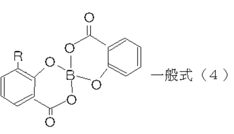
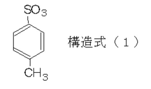


<6> 消色性色素が、下記構造式(5)~(7)で表される化合物から選択された少なくとも1種を含む前記<1>に記載の接続フィルムである。


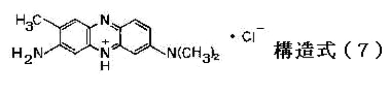
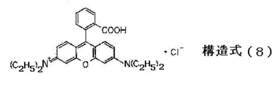



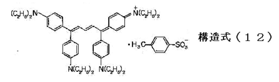
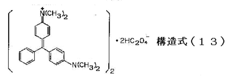
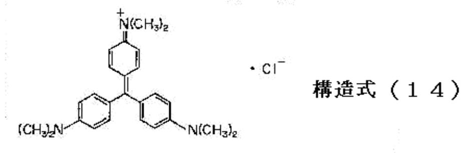
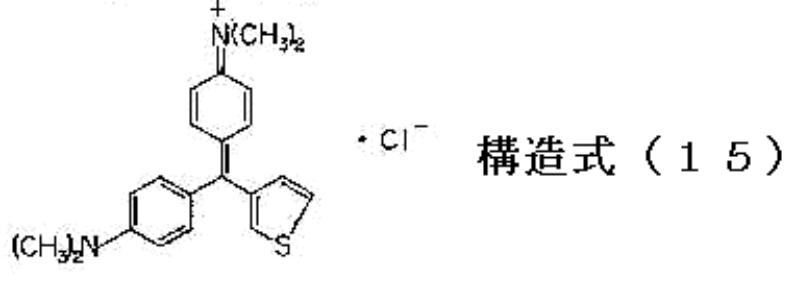

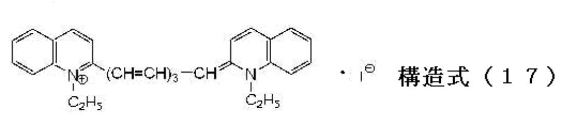

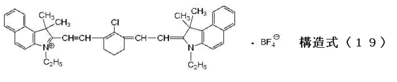

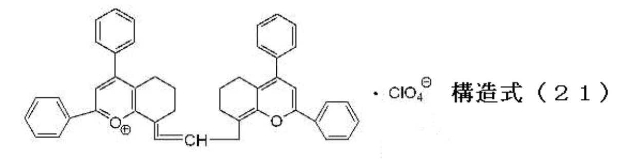
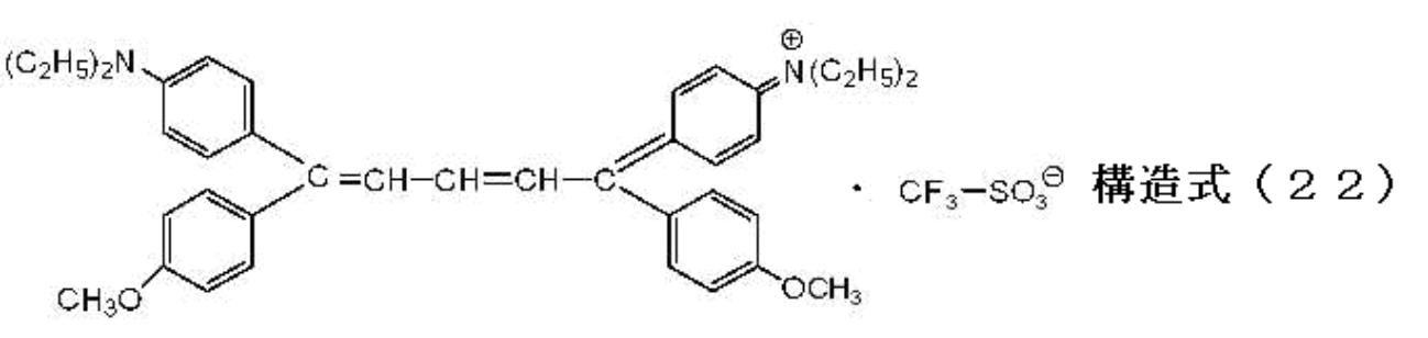
<16> 硬化性有機樹脂がエポキシ樹脂であり、硬化剤がカチオン硬化剤である前記<1>から<14>のいずれかに記載の接続フィルムである。
<17> 前記<1>から<16>のいずれかに記載の接続フィルムを介して、第1及び第2の基板を加熱乃至光照射しながら圧着して接合する接続工程を含み、前記接続工程において、前記有機樹脂層の硬化反応が終了したときに、前記消色性色素が消色していることを特徴とする接合体の製造方法である。
<18> 前記<17>に記載の接合体の製造方法により製造されたことを特徴とする接合体である。
本発明の接合体は、第1の基板(第1の回路部材)と、第2の基板(第2の回路部材)と、接続フィルムとを有してなり、さらに、必要に応じて適宜選択した、その他の部材を有してなる。
例えば、図1に示すように、接合体100は、第1の基板(第1の回路部材)10と、第2の基板(第2の回路部材)11と、接続フィルム12(後述する有機樹脂層21)とを有する。第2の基板(第2の回路部材)11における端子11aと、接続フィルム12中に分散された導電性粒子12aと、第1の基板(第1の回路部材)10における端子(不図示)とが導通されることにより、第1の基板(第1の回路部材)10と第2の基板(第2の回路部材)11とが電気的に接続される。
前記第1の基板(第1の回路部材)としては、特に制限はなく、目的に応じて適宜選択することができ、例えば、FPC基板、PWB基板、ガラス製のLCD基板(LCDパネル)、ガラス製のPDP基板(PDPパネル)、ガラス製の有機EL基板(有機ELパネル)等が挙げられる。
前記第2の基板(第2の回路部材)としては、特に制限はなく、目的に応じて適宜選択することができ、例えば、FPC基板、COF基板、TCP基板、PWB基板、IC基板等が挙げられる。
前記接続フィルムは、有機樹脂層を有してなり、さらに、必要に応じて適宜選択した、その他の層を有してなる。前記有機樹脂層は、導電性粒子を含有する導電性粒子含有有機樹脂層である。
例えば、図2に示すように、接続フィルム12は、剥離層(セパレータ)20と、剥離層(セパレータ)20上に形成された導電性粒子含有有機樹脂層21とを有する。
前記有機樹脂層としては、前記第1の基板(第1の回路部材)及び前記第2の基板(第2の回路部材)間に配置され、消色性色素、硬化性有機樹脂、硬化剤及び導電性粒子を含有するものであれば、特に制限はなく、目的に応じて適宜選択することができ、例えば、シランカップリング剤、界面活性剤などをさらに含有していてもよい。
また、前記有機樹脂層は、単層であっても複数層であってもよい。有機樹脂層が複数層である場合において、消色性色素、硬化性有機樹脂、硬化剤及び導電性粒子は、それぞれ、同一層に含まれていてもよく、異なる層に含まれていてもよい。
また、有機樹脂層を形成する接合材料は、ペースト状であってもフィルム状であってもよい。
前記消色性色素としては、接続フィルムを圧着した後に消色するもの(無色に変色するもののみならず、後述する導電性微粒子の色(薄黄色)と同系統の色(黄色乃至薄黄色)に変色するもの)であれば、特に制限はなく、目的に応じて適宜選択することができ、例えば、アミノ基または誘導アミノ基を有するジアリールメタン系色素、トリアリールメタン系色素、シアニン系色素、ポリメチン系色素、及びキサンテン、アジン、アクリジン、チアジン、オキサジンのいずれか1つ以上を骨格に有する複素環色素などが挙げられ、より具体的には、下記一般式(1)、(2)及び(5)~(7)で表される化合物、下記構造式(3)~(23)で表される化合物などが挙げられる。これらの消色性色素は、1種のみ含まれていてもよく、また、2種以上含まれていてもよい。さらに、これらの消色性色素のカチオン部(カウンターアニオン以外の部分)が複数含まれていてもよい。
また、前記消色性色素の好ましい含有量としては、有機樹脂層に含まれるバインダー(硬化性樹脂及びその他の樹脂を含む)全体100質量部に対して0.5質量部~3.0質量部が好ましく、有機樹脂層に含まれる硬化性樹脂100質量部に対して3.0質量部~6.0質量部が好ましい。








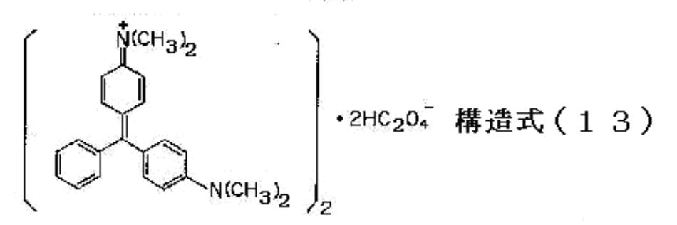

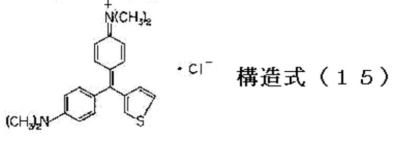

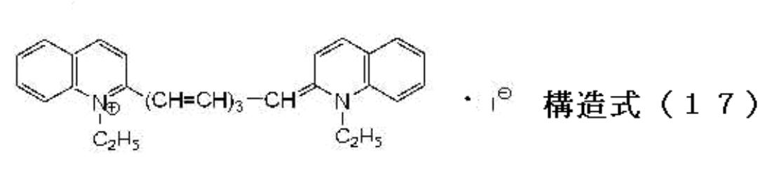


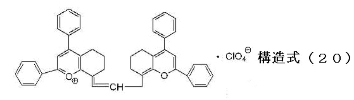


前記消色性色素の消色原理を以下に説明する。
ラジカル反応における消色反応は、下記反応式(1)に示されるように、熱乃至光によりラジカル系硬化剤が解離して、ラジカルを放出し、該放出されたラジカルと消色性色素とが結合することによるものと考えられる。


前記硬化性有機樹脂としては、特に制限はなく、目的に応じて適宜選択することができるが、熱硬化性有機樹脂が好ましく、アクリル樹脂、エポキシ樹脂などがより好ましい。
前記アクリル樹脂としては、特に制限はなく、目的に応じて適宜選択することができ、例えば、メチルアクリレート、エチルアクリレート、イソプロピルアクリレート、イソブチルアクリレート、エポキシアクリレート、エチレングリコールジアクリレート、ジエチレングリコールジアクリレート、トリメチロールプロパントリアクリレート、ジメチロールトリシクロデカンジアクリレート、テトラメチレングリコールテトラアクリレート、2-ヒドロキシ-1,3-ジアクリロキシプロパン、2,2-ビス[4-(アクリロキシメトキシ)フェニル]プロパン、2,2-ビス[4-(アクリロキシエトキシ)フェニル]プロパン、ジシクロペンテニルアクリレート、トリシクロデカニルアクリレート、トリス(アクリロキシエチル)イソシアヌレート、ウレタンアクリレートなどのアクリル樹脂が挙げられる。これらは、1種単独で使用してもよいし、2種以上を併用してもよい。
また、前記アクリレートをメタクリレートにしたものが挙げられ、これらは、1種単独で使用してもよいし、2種以上を併用してもよい。
前記エポキシ樹脂としては、特に制限はなく、目的に応じて適宜選択することができ、例えば、ビスフェノールA型エポキシ樹脂、ビスフェノールF型エポキシ樹脂、ノボラック型エポキシ樹脂や、それらの変性エポキシ樹脂などの熱硬化性エポキシ樹脂が挙げられる。これらは、1種単独で使用してもよいし、2種以上を併用してもよい。
前記硬化剤としては、特に制限はなく、目的に応じて適宜選択することができるが、硬化性有機樹脂がアクリル樹脂の場合はラジカル系硬化剤が好ましく、硬化性有機樹脂がエポキシ樹脂の場合はカチオン系硬化剤が好ましい。
前記ラジカル系硬化剤としては、特に制限はなく、目的に応じて適宜選択することができ、例えば、有機過酸化物を挙げることができる。
前記カチオン系硬化剤としては、特に制限はなく、目的に応じて適宜選択することができ、例えば、スルホニウム塩、オニウム塩等を挙げることができ、これらの中でも、芳香族スルホニウム塩が好ましい。
前記導電性粒子としては、特に制限はなく、従来の異方性導電接着剤(接続フィルム)において用いられているものが利用でき、例えば、粒子の直径が1~50μmの金属粒子又は金属被覆樹脂粒子を使用することができる。
前記金属粒子としては、ニッケル、コバルト、銅等が挙げられる。それらの表面酸化を防ぐ目的で、表面に金、パラジウムをコーティングした粒子を用いてもよい。さらに、表面に金属突起や有機物で絶縁皮膜を施したものを用いてもよい。
前記金属被覆樹脂粒子としては、ニッケル、コバルト、銅等の1種以上でメッキを施した真球状の粒子が挙げられる。同様に、最外表面に金、パラジウムをコーティングした粒子を用いてもよい。さらに、表面に金属突起や有機物で絶縁皮膜を施したものを用いてもよい。
前記その他の層としては、特に制限はなく、目的に応じて適宜選択することができ、例えば、剥離層を挙げることができる。
前記剥離層としては、その形状、構造、大きさ、厚み、材料(材質)などについては、特に制限はなく、目的に応じて適宜選択することができるが、剥離性の良好なものや耐熱性が高いものが好ましく、例えば、シリコーン等の剥離剤が塗布された透明な剥離PET(ポリエチレンテレフタレート)シートなどが好適に挙げられる。また、PTFE(ポリテトラフルオロエチレン)シートを用いてもよい。
前記その他の部材としては、特に制限はなく、目的に応じて適宜選択することができる。
本発明の接合体の製造方法は、少なくとも接合工程を含み、さらに、必要に応じて適宜選択した、その他の工程を含む。
前記接合工程は、本発明の接続フィルムを介して、第1及び第2の基板を加熱乃至光照射しながら圧着して接合する工程である。
前記加熱は、トータル熱量により決定され、接続時間10秒以下で接合を完了する場合は、加熱温度120℃~220℃で行われる。
前記光照射は、水銀ランプ、メタルハライドランプ等のUV照射装置で行われる。
前記圧着は、第2の基板の種類によって異なり、第2の基板がFPC、TAB(Tape Automated Bonding)である場合は圧力2MPa~6MPaで、第2の基板がICチップである場合は圧力30MPa~150MPaで、それぞれ3秒間~10秒間行われる。
なお、接合を超音波を用いて行ってもよい。
フェノキシ樹脂(品名:YP50、東都化成社製)60部と、硬化性樹脂としてのラジカル重合性樹脂(品名:EB-600、ダイセル・サイテック社製)35部と、シランカップリング剤(品名:KBM-503、信越化学工業社製)2部と、ラジカル硬化剤としての反応開始剤(品名:パーヘキサC、10時間半減期温度90.7℃、日本油脂社製)3部とで構成された接着剤中に導電性粒子(品名:AUL704、積水化学工業社製)を粒子密度10,000個/mm2になるよう分散させた厚み15μmのラジカル接合材料R1を得た。このラジカル接合材料R1は導電性粒子の色である薄黄色であった(図3における(1)参照)。
ラジカル接合材料R1に、キノン系色素(C.I Solvent Blue 35:AMMONIUM,ETHYL(4-(p-(ETHYL(m-SULFOBENZYL)AMINO)-alpha-(o-SULFOPHENYL)BENZYLIDENE)-2,5-CYCLOHEXADIEN-1-YLIDENE)(m-SULFOBENZYL)-,HYDROXIDE、保土谷化学工業製)を1部含有させたラジカル接合材料R2を得た。このラジカル接合材料R2の色は青色であった(図3における(3)参照)。
ラジカル接合材料R1に、トリフェニルメタン系色素(C.I Solvent Red 18:AMMONIUM,(6-(DIETHYLAMINO)-9-(2,4-DISULFOPHENYL)-3H-XANTHEN-3-YLIDENE)DIETHYL-, HYDROXIDE、保土谷化学工業製)を1部含有させたラジカル接合材料R3を得た。このラジカル接合材料R3の色は赤色であった。(図3における(4)参照)。
フェノキシ樹脂(品名:YP50、東都化成社製)60部と、硬化性樹脂としてのエポキシ樹脂(品名:EP-828、ジャパンエポキシレジン社製)35部と、シランカップリング剤(品名:KBM-403、信越化学工業社製)2部と、カチオン硬化剤としての反応開始剤(品名:SI-80L、三新化学社製)3部とで構成された接着剤中に導電性粒子(品名:AUL704、積水化学工業社製)を粒子密度10,000個/mm2になるよう分散させた厚み15μmのカチオン接合材料C1を得た。このカチオン接合材料C1は導電性粒子の色である薄黄色であった。
ラジカル接合材料R1に、R1、R2、Y、n、Zが表1の構造である下記一般式(1)の色素P1~P10をそれぞれ各1部ずつ含有させたラジカル接合材料A1~A10を得た。これらのラジカル接合材料A1~A10の色はどれも青色であった。ラジカル接合材料A2(色素としてP2(1,1,5,5,-テトラキス[4-(ジエチルアミノ)フェニル]-1,4-ペンタジエン-3-イリウム-p-トルエンスルホナート)を用いた接合材料)の写真を図3における(2)に示す。


ラジカル接合材料A1の作製において、反応開始剤としてパーヘキサC(10時間半減期温度90.7℃、日本油脂社製)を用いる代わりに、パーオクタND(10時間半減期温度40.7℃、日本油脂社製)を用いた以外は、ラジカル接合材料A1の作製と同様にして、ラジカル接合材料A11を得た。
ラジカル接合材料A1の作製において、反応開始剤としてパーヘキサC(10時間半減期温度90.7℃、日本油脂社製)を用いる代わりに、パーヘキシン25B(10時間半減期温度128.4℃、日本油脂社製)を用いた以外は、ラジカル接合材料A1の作製と同様にして、ラジカル接合材料A12を得た。
ラジカル接合材料R1に下記構造式(7)~(9)、(12)、(13)の色素P11~P15をそれぞれ各1部ずつさらに含有させたラジカル接合材料A13~A17を得た。



カチオン接合材料C1の作製において、下記構造式(12)の色素P14を1部をさらに含有させたカチオン接合材料A18を得た。

(接合体の作製)
COF基板(ソニーケミカル&インフォメーションデバイス株式会社評価用基材、50μmP、Snメッキされた8μm厚のCu、38μm厚のS’perflex基材)と、ITOコーテティングガラス(ソニーケミカル&インフォメーションデバイス株式会社評価用基材、全表面ITOコート、ガラス厚0.7mm)との接合をおこなった。まず、ITOコーティングガラス上に1.5mm幅にスリットされたラジカル接合材料A1をラミネートし、その上にCOF基板を仮固定した後、1.5mm幅のヒートツールで、緩衝材(100μm厚テフロン(登録商標))を用いて、接合条件190℃‐3MPa-10秒間で接合を行い、接合体AJ1を得た。
作製した接合体AJ1における接続フィルムについて目視で消色具合を確認した。結果を表2に示す。
作製した接合体AJ1について、デジタルマルチメータ(品番:デジタルメルチメータ7555、横河電機社製)を用いて4端子法にて電流1mAを流したときの接合抵抗の抵抗値(Ω)の測定をおこなった。結果を表2に示す。
作製した接合体AJ1について、引っ張り試験機(品番:RTC1201、AND社製)を用いて測定速度50mm/secでCOF基板を引き上げたときのCOF基板とITOコーティングガラスの接着強度測定をおこなった。結果を表2に示す。
実施例1において、ラジカル接合材料A1を用いる代わりに、ラジカル接合材料A2を用いた以外は、実施例1と同様にして接合体を作製し、接合体AJ2を得た。また、実施例1と同様に、実装後の消色確認(図5参照)、接合体の接続抵抗測定、接合体の接着強度測定を行った。結果を表2に示す。
実施例1において、ラジカル接合材料A1を用いる代わりに、ラジカル接合材料A3を用いた以外は、実施例1と同様にして接合体を作製し、接合体AJ3を得た。また、実施例1と同様に、実装後の消色確認、接合体の接続抵抗測定、接合体の接着強度測定を行った。結果を表2に示す。
実施例1において、ラジカル接合材料A1を用いる代わりに、ラジカル接合材料A4を用いた以外は、実施例1と同様にして接合体を作製し、接合体AJ4を得た。また、実施例1と同様に、実装後の消色確認、接合体の接続抵抗測定、接合体の接着強度測定を行った。結果を表2に示す。
実施例1において、ラジカル接合材料A1を用いる代わりに、ラジカル接合材料A5を用いた以外は、実施例1と同様にして接合体を作製し、接合体AJ5を得た。また、実施例1と同様に、実装後の消色確認、接合体の接続抵抗測定、接合体の接着強度測定を行った。結果を表2に示す。
実施例1において、ラジカル接合材料A1を用いる代わりに、ラジカル接合材料A6を用いた以外は、実施例1と同様にして接合体を作製し、接合体AJ6を得た。また、実施例1と同様に、実装後の消色確認、接合体の接続抵抗測定、接合体の接着強度測定を行った。結果を表2に示す。
実施例1において、ラジカル接合材料A1を用いる代わりに、ラジカル接合材料A7を用いた以外は、実施例1と同様にして接合体を作製し、接合体AJ7を得た。また、実施例1と同様に、実装後の消色確認、接合体の接続抵抗測定、接合体の接着強度測定を行った。結果を表2に示す。
実施例1において、ラジカル接合材料A1を用いる代わりに、ラジカル接合材料A8を用いた以外は、実施例1と同様にして接合体を作製し、接合体AJ8を得た。また、実施例1と同様に、実装後の消色確認、接合体の接続抵抗測定、接合体の接着強度測定を行った。結果を表2に示す。
実施例1において、ラジカル接合材料A1を用いる代わりに、ラジカル接合材料A9を用いた以外は、実施例1と同様にして接合体を作製し、接合体AJ9を得た。また、実施例1と同様に、実装後の消色確認、接合体の接続抵抗測定、接合体の接着強度測定を行った。結果を表2に示す。
実施例1において、ラジカル接合材料A1を用いる代わりに、ラジカル接合材料A10を用いた以外は、実施例1と同様にして接合体を作製し、接合体AJ10を得た。また、実施例1と同様に、実装後の消色確認、接合体の接続抵抗測定、接合体の接着強度測定を行った。結果を表2に示す。
実施例1において、ラジカル接合材料A1を用いる代わりに、ラジカル接合材料A11を用いた以外は、実施例1と同様にして接合体を作製し、接合体AJ11を得た。また、実施例1と同様に、実装後の消色確認、接合体の接続抵抗測定、接合体の接着強度測定を行った。結果を表2に示す。
実施例1において、ラジカル接合材料A1を用いる代わりに、ラジカル接合材料A12を用いた以外は、実施例1と同様にして接合体を作製し、接合体AJ12を得た。また、実施例1と同様に、実装後の消色確認、接合体の接続抵抗測定、接合体の接着強度測定を行った。結果を表2に示す。
比較例1において、ラジカル接合材料A1を用いる代わりに、ラジカル接合材料R1を用いた以外は、実施例1と同様にして接合体を作製し、接合体RJ1を得た。また、実施例1と同様に、実装後の消色確認、接合体の接続抵抗測定、接合体の接着強度測定を行った。結果を表2に示す。

実施例1において、ラジカル接合材料A1を用いる代わりに、ラジカル接合材料A13を用いた以外は、実施例1と同様にして接合体を作製し、接合体AJ13を得た。また、実施例1と同様に、実装後の消色確認、接合体の接続抵抗測定、接合体の接着強度測定を行った。結果を表3に示す。
実施例1において、ラジカル接合材料A1を用いる代わりに、ラジカル接合材料A14を用いた以外は、実施例1と同様にして接合体を作製し、接合体AJ14を得た。また、実施例1と同様に、実装後の消色確認、接合体の接続抵抗測定、接合体の接着強度測定を行った。結果を表3に示す。
実施例1において、ラジカル接合材料A1を用いる代わりに、ラジカル接合材料A15を用いた以外は、実施例1と同様にして接合体を作製し、接合体AJ15を得た。また、実施例1と同様に、実装後の消色確認、接合体の接続抵抗測定、接合体の接着強度測定を行った。結果を表3に示す。
実施例1において、ラジカル接合材料A1を用いる代わりに、ラジカル接合材料A16を用いた以外は、実施例1と同様にして接合体を作製し、接合体AJ16を得た。また、実施例1と同様に、実装後の消色確認、接合体の接続抵抗測定、接合体の接着強度測定を行った。結果を表3に示す。
実施例1において、ラジカル接合材料A1を用いる代わりに、ラジカル接合材料A17を用いた以外は、実施例1と同様にして接合体を作製し、接合体AJ17を得た。また、実施例1と同様に、実装後の消色確認、接合体の接続抵抗測定、接合体の接着強度測定を行った。結果を表3に示す。
実施例1において、ラジカル接合材料A1を用いる代わりに、カチオン接合材料A18を用いた以外は、実施例1と同様にして接合体を作製し、接合体AJ18を得た。また、実施例1と同様に、実装後の消色確認、接合体の接続抵抗測定、接合体の接着強度測定を行った。結果を表3に示す。
(接合体の作製)
COF基板(ソニーケミカル&インフォメーションデバイス株式会社評価用基材、50μmP、Snメッキされた8μm厚のCu、38μm厚のS’perflex基材)と、ITOコーテティングガラス((ソニーケミカル&インフォメーションデバイス株式会社評価用基材、全表面ITOコート、ガラス厚0.7mm)との接合をおこなった。まず、ITOコーティングガラス上に1.5mm幅にスリットされたカチオン接合材料A18をラミネートし、その上にCOF基板を仮固定したものをITOコーテティングガラス上に載置し、緩衝材(100μm厚テフロン(登録商標))を被せて、1.5mm幅のツールで5MPaの力でCOF基板を押し込んだ状態で、ITOコーティングガラス側からメタルハライドランプを用いて光量3,000mJ/cm2にて20秒間照射して接合を行い、接合体AJ19を得た。
作製した接合体AJ19における接続フィルム接合材料A18について目視で消色具合を確認した。結果を表3に示す。
作製した接合体AJ19について、デジタルマルチメータ(品番:デジタルメルチメータ7555、横河電機社製)を用いて4端子法にて電流1mAを流したときの接合抵抗の抵抗値(Ω)の測定をおこなった。結果を表3に示す。
作製した接合体AJ19について、引っ張り試験機(品番:RTC1201、AND社製)を用いて測定速度50mm/secでCOF基板を引き上げたときのCOF基板とITOコーティングガラスの接着強度測定をおこなった。結果を表3に示す。
実施例18において、カチオン接合材料A18を用いる代わりに、カチオン接合材料C1を用いた以外は、実施例18と同様にして接合体を作製し、接合体CJ1を得た。また、実施例18と同様に、実装後の消色確認、接合体の接続抵抗測定、接合体の接着強度測定を行った。結果を表3に示す。

実施例1において、ラジカル接合材料A1を用いる代わりに、ラジカル接合材料R2を用いた以外は、実施例1と同様にして接合体を作製し、接合体RJ2を得た。また、実施例1と同様に、実装後の消色確認(図6参照)、接合体の接続抵抗測定、接合体の接着強度測定を行った。結果を表4に示す。
実施例1において、ラジカル接合材料A1を用いる代わりに、ラジカル接合材料R3を用いた以外は、実施例1と同様にして接合体を作製し、接合体RJ3を得た。また、実施例1と同様に、実装後の消色確認(図7参照)、接合体の接続抵抗測定、接合体の接着強度測定を行った。結果を表4に示す。

一方、比較例1では、ラジカル接合材料R1には色素が含有されておらず、薄黄色であるため(図3における(1))、接着フィルムの貼付位置を明確に判別することができず、また、圧着後における接着フィルムの硬化度についても目視で確認することができなかった(図4参照)。なお、比較例2についても同様であった。
また、比較例3及び4では、ラジカル接合材料R2及びR3に含有される色素が圧着後においても消色しないため(図6及び図7参照)、接合体RJ2及びRJ3の接合面の外観検査(導電性粒子の数及び潰れ状態の検査など)、接合体RJ2及びRJ3の腐食性試験における腐食性部分の判別が困難であった。
11 第2の基板
11a 端子
12 接続フィルム
12a 導電性粒子
20 剥離層(セパレータ)
21 有機樹脂層
100 接合体
Claims (18)
- 消色性色素、硬化性有機樹脂、硬化剤及び導電性粒子を含有する有機樹脂層を有することを特徴とする接続フィルム。
- 消色性色素が、下記一般式(1)で表される化合物を含む請求項1に記載の接続フィルム。

- 消色性色素が、下記一般式(2)で表される化合物を含む請求項1に記載の接続フィルム。

- Zが、ClO4、BF4、CF3SO3、下記一般式(3)で表される化合物、下記一般式(4)で表される化合物、下記構造式(1)で表される化合物及び下記構造式(2)で表される化合物のいずれかである請求項2から3のいずれかに記載の接続フィルム。


- 消色性色素が、下記一般式(5)で表される化合物、下記一般式(6)で表される化合物、下記構造式(3)で表される化合物、下記構造式(4)で表される化合物、及び下記一般式(7)で表される化合物から選択された少なくとも1種を含む請求項1に記載の接続フィルム。



- 消色性色素が、下記構造式(5)~(7)で表される化合物から選択された少なくとも1種を含む請求項1に記載の接続フィルム。



- 消色性色素が、下記構造式(8)~(9)で表される化合物から選択された少なくとも1種を含む請求項1に記載の接続フィルム。
- 消色性色素が、下記構造式(10)~(11)で表される化合物から選択された少なくとも1種を含む請求項1に記載の接続フィルム。


- 消色性色素が、下記構造式(12)で表される化合物を含む請求項1に記載の接続フィルム。
- 消色性色素が、下記構造式(13)~(15)で表される化合物から選択された少なくとも1種を含む請求項1に記載の接続フィルム。

- 消色性色素が、下記構造式(16)~(17)で表される化合物から選択された少なくとも1種を含む請求項1に記載の接続フィルム。


- 消色性色素が、下記構造式(18)~(19)で表される化合物から選択された少なくとも1種を含む請求項1に記載の接続フィルム。


- 消色性色素が、下記構造式(20)~(21)で表される化合物から選択された少なくとも1種を含む請求項1に記載の接続フィルム。

- 消色性色素が、下記構造式(22)~(23)で表される化合物から選択された少なくとも1種を含む請求項1に記載の接続フィルム。

- 硬化性有機樹脂がアクリル樹脂であり、硬化剤がラジカル硬化剤である請求項1から14のいずれかに記載の接続フィルム。
- 硬化性有機樹脂がエポキシ樹脂であり、硬化剤がカチオン硬化剤である請求項1から14のいずれかに記載の接続フィルム。
- 請求項1から16のいずれかに記載の接続フィルムを介して、第1及び第2の基板を加熱乃至光照射しながら圧着して接合する接続工程を含み、
前記接続工程において、前記有機樹脂層の硬化反応が終了したときに、前記消色性色素が消色していることを特徴とする接合体の製造方法。 - 請求項17に記載の接合体の製造方法により製造されたことを特徴とする接合体。
Priority Applications (3)
| Application Number | Priority Date | Filing Date | Title |
|---|---|---|---|
| CN200980148326.6A CN102232096B (zh) | 2008-12-01 | 2009-11-24 | 连接膜和接合体及其制造方法 |
| KR1020117014540A KR101350681B1 (ko) | 2008-12-01 | 2009-11-24 | 접속 필름과, 접합체 및 그 제조 방법 |
| US13/116,265 US8309638B2 (en) | 2008-12-01 | 2011-05-26 | Connecting film, and joined structure and method for producing the same |
Applications Claiming Priority (2)
| Application Number | Priority Date | Filing Date | Title |
|---|---|---|---|
| JP2008306292A JP2010129960A (ja) | 2008-12-01 | 2008-12-01 | 接続フィルム、並びに、接合体及びその製造方法 |
| JP2008-306292 | 2008-12-01 |
Related Child Applications (1)
| Application Number | Title | Priority Date | Filing Date |
|---|---|---|---|
| US13/116,265 Continuation US8309638B2 (en) | 2008-12-01 | 2011-05-26 | Connecting film, and joined structure and method for producing the same |
Publications (1)
| Publication Number | Publication Date |
|---|---|
| WO2010064560A1 true WO2010064560A1 (ja) | 2010-06-10 |
Family
ID=42233212
Family Applications (1)
| Application Number | Title | Priority Date | Filing Date |
|---|---|---|---|
| PCT/JP2009/069798 Ceased WO2010064560A1 (ja) | 2008-12-01 | 2009-11-24 | 接続フィルム、並びに、接合体及びその製造方法 |
Country Status (6)
| Country | Link |
|---|---|
| US (1) | US8309638B2 (ja) |
| JP (1) | JP2010129960A (ja) |
| KR (1) | KR101350681B1 (ja) |
| CN (1) | CN102232096B (ja) |
| TW (1) | TWI468486B (ja) |
| WO (1) | WO2010064560A1 (ja) |
Cited By (1)
| Publication number | Priority date | Publication date | Assignee | Title |
|---|---|---|---|---|
| JP2021134350A (ja) * | 2020-02-21 | 2021-09-13 | Jsr株式会社 | 樹脂組成物、化合物(Z)、基材(i)、光学フィルターおよびその用途 |
Families Citing this family (6)
| Publication number | Priority date | Publication date | Assignee | Title |
|---|---|---|---|---|
| EP2463107B1 (en) * | 2010-12-09 | 2014-07-16 | Kabushiki Kaisha Toshiba | Color erasing apparatus and control method of the color erasing apparatus |
| KR101774624B1 (ko) * | 2011-08-05 | 2017-09-04 | 세키스이가가쿠 고교가부시키가이샤 | 도전 재료 및 접속 구조체 |
| CN104157627B (zh) * | 2013-05-14 | 2019-11-08 | 飞兆半导体公司 | 半导体组件 |
| JP6331776B2 (ja) | 2014-06-30 | 2018-05-30 | デクセリアルズ株式会社 | 異方導電性フィルム及び接続構造体 |
| KR101744821B1 (ko) | 2015-12-22 | 2017-06-08 | 현대자동차 주식회사 | 초박형 스위치 및 이의 제조방법 |
| CN111295723B (zh) | 2018-03-14 | 2022-06-14 | 株式会社Lg化学 | 嵌入式透明电极基板及其制造方法 |
Citations (5)
| Publication number | Priority date | Publication date | Assignee | Title |
|---|---|---|---|---|
| JPS6245657A (ja) * | 1985-08-26 | 1987-02-27 | Toshiba Silicone Co Ltd | ポリオルガノシロキサン組成物 |
| JPH08120227A (ja) * | 1994-10-25 | 1996-05-14 | Three Bond Co Ltd | 紫外線吸収性光硬化型接着剤組成物 |
| JPH11307154A (ja) * | 1998-04-16 | 1999-11-05 | Fujikura Ltd | 異方導電性材料 |
| JP2004140366A (ja) * | 2003-10-15 | 2004-05-13 | Hitachi Chem Co Ltd | 電極の接続方法 |
| JP2008069307A (ja) * | 2006-09-15 | 2008-03-27 | Dh Material Kk | 被覆接着用ラジカル重合性樹脂組成物 |
Family Cites Families (4)
| Publication number | Priority date | Publication date | Assignee | Title |
|---|---|---|---|---|
| JPH07123179B2 (ja) | 1990-10-05 | 1995-12-25 | 信越ポリマー株式会社 | 異方導電接着剤による回路基板の接続構造 |
| JPH05132655A (ja) | 1991-11-12 | 1993-05-28 | Mita Ind Co Ltd | 接着剤 |
| JP2002139833A (ja) * | 2000-11-02 | 2002-05-17 | Fuji Photo Film Co Ltd | 光重合性組成物および感光感熱記録材料 |
| JP2007091798A (ja) | 2005-09-27 | 2007-04-12 | Sony Chemical & Information Device Corp | 発色剤、発色剤セット、接着剤、接着剤セット及び接着方法 |
-
2008
- 2008-12-01 JP JP2008306292A patent/JP2010129960A/ja active Pending
-
2009
- 2009-11-24 CN CN200980148326.6A patent/CN102232096B/zh active Active
- 2009-11-24 KR KR1020117014540A patent/KR101350681B1/ko active Active
- 2009-11-24 WO PCT/JP2009/069798 patent/WO2010064560A1/ja not_active Ceased
- 2009-11-30 TW TW98140994A patent/TWI468486B/zh active
-
2011
- 2011-05-26 US US13/116,265 patent/US8309638B2/en active Active
Patent Citations (5)
| Publication number | Priority date | Publication date | Assignee | Title |
|---|---|---|---|---|
| JPS6245657A (ja) * | 1985-08-26 | 1987-02-27 | Toshiba Silicone Co Ltd | ポリオルガノシロキサン組成物 |
| JPH08120227A (ja) * | 1994-10-25 | 1996-05-14 | Three Bond Co Ltd | 紫外線吸収性光硬化型接着剤組成物 |
| JPH11307154A (ja) * | 1998-04-16 | 1999-11-05 | Fujikura Ltd | 異方導電性材料 |
| JP2004140366A (ja) * | 2003-10-15 | 2004-05-13 | Hitachi Chem Co Ltd | 電極の接続方法 |
| JP2008069307A (ja) * | 2006-09-15 | 2008-03-27 | Dh Material Kk | 被覆接着用ラジカル重合性樹脂組成物 |
Cited By (2)
| Publication number | Priority date | Publication date | Assignee | Title |
|---|---|---|---|---|
| JP2021134350A (ja) * | 2020-02-21 | 2021-09-13 | Jsr株式会社 | 樹脂組成物、化合物(Z)、基材(i)、光学フィルターおよびその用途 |
| JP7630759B2 (ja) | 2020-02-21 | 2025-02-18 | Jsr株式会社 | 樹脂組成物、化合物(Z)、基材(i)、光学フィルターおよびその用途 |
Also Published As
| Publication number | Publication date |
|---|---|
| JP2010129960A (ja) | 2010-06-10 |
| TW201030120A (en) | 2010-08-16 |
| CN102232096A (zh) | 2011-11-02 |
| US20110223430A1 (en) | 2011-09-15 |
| US8309638B2 (en) | 2012-11-13 |
| KR101350681B1 (ko) | 2014-01-10 |
| CN102232096B (zh) | 2014-05-07 |
| TWI468486B (zh) | 2015-01-11 |
| KR20110089875A (ko) | 2011-08-09 |
Similar Documents
| Publication | Publication Date | Title |
|---|---|---|
| WO2010064560A1 (ja) | 接続フィルム、並びに、接合体及びその製造方法 | |
| JP4897778B2 (ja) | 接続フィルム、並びに、接合体及びその製造方法 | |
| TWI452401B (zh) | 異向性導電膜及接合體及其製造方法 | |
| JP6036694B2 (ja) | 接着材リール、ブロッキング抑制方法、接着材リールの交換方法、接着材テープの繰出し方法、接着材リールの製造方法、リールキット、及び梱包体 | |
| JP5093482B2 (ja) | 異方性導電材料、接続構造体及びその製造方法 | |
| KR100359175B1 (ko) | 이방성전기전도성접착제필름 | |
| JP5823117B2 (ja) | 異方性導電フィルム、接合体、及び接合体の製造方法 | |
| CN103597667B (zh) | 膜状电路连接材料和电路连接结构体 | |
| KR101410185B1 (ko) | 이방성 도전 접착 필름, 접속 구조체 및 그 제조 방법 | |
| CN102948265B (zh) | 接合体及其制造方法 | |
| US20100252783A1 (en) | Ambient-curable anisotropic conductive adhesive | |
| JP2001126541A (ja) | 異方導電フィルム及び電気・電子部品 | |
| JP5539039B2 (ja) | 異方性導電フィルム及びその製造方法 | |
| KR102629573B1 (ko) | 블랙 색상을 가지는 이방도전성 접착필름 | |
| WO2016052130A1 (ja) | 異方性導電フィルム、及び接続方法 | |
| JP5558184B2 (ja) | 異方性導電フィルム、接合体及び接続方法 | |
| JP2010135255A (ja) | 異方性導電フィルム、並びに、接合体及びその製造方法 | |
| JP4867069B2 (ja) | 接着剤組成物、それを用いた回路端子の接続方法及び回路端子の接続構造 | |
| JP4538266B2 (ja) | 接着フィルム、接着剤付き基板の製造方法、及び接着フィルムの製造方法 | |
| TWI814761B (zh) | 接著劑膜 | |
| CN107005012A (zh) | 连接体的检查方法、连接体、导电性粒子及各向异性导电粘接剂 | |
| JP2004269626A (ja) | 接着剤、接着剤の製造方法及び電気装置 | |
| JP2002203871A (ja) | 接着剤組成物、それを用いた回路端子の接続方法及び回路端子の接続構造 | |
| JP2016201254A (ja) | 異方性導電フィルム、及び接続方法 |
Legal Events
| Date | Code | Title | Description |
|---|---|---|---|
| WWE | Wipo information: entry into national phase |
Ref document number: 200980148326.6 Country of ref document: CN |
|
| 121 | Ep: the epo has been informed by wipo that ep was designated in this application |
Ref document number: 09830327 Country of ref document: EP Kind code of ref document: A1 |
|
| NENP | Non-entry into the national phase |
Ref country code: DE |
|
| ENP | Entry into the national phase |
Ref document number: 20117014540 Country of ref document: KR Kind code of ref document: A |
|
| 122 | Ep: pct application non-entry in european phase |
Ref document number: 09830327 Country of ref document: EP Kind code of ref document: A1 |