WO2010058656A1 - インターフェイス装置 - Google Patents
インターフェイス装置 Download PDFInfo
- Publication number
- WO2010058656A1 WO2010058656A1 PCT/JP2009/066898 JP2009066898W WO2010058656A1 WO 2010058656 A1 WO2010058656 A1 WO 2010058656A1 JP 2009066898 W JP2009066898 W JP 2009066898W WO 2010058656 A1 WO2010058656 A1 WO 2010058656A1
- Authority
- WO
- WIPO (PCT)
- Prior art keywords
- load lock
- transfer
- substrate
- chamber
- wafer
- Prior art date
- Legal status (The legal status is an assumption and is not a legal conclusion. Google has not performed a legal analysis and makes no representation as to the accuracy of the status listed.)
- Ceased
Links
Images

Classifications
-
- H—ELECTRICITY
- H10—SEMICONDUCTOR DEVICES; ELECTRIC SOLID-STATE DEVICES NOT OTHERWISE PROVIDED FOR
- H10P—GENERIC PROCESSES OR APPARATUS FOR THE MANUFACTURE OR TREATMENT OF DEVICES COVERED BY CLASS H10
- H10P76/00—Manufacture or treatment of masks on semiconductor bodies, e.g. by lithography or photolithography
- H10P76/20—Manufacture or treatment of masks on semiconductor bodies, e.g. by lithography or photolithography of masks comprising organic materials
- H10P76/204—Manufacture or treatment of masks on semiconductor bodies, e.g. by lithography or photolithography of masks comprising organic materials of organic photoresist masks
- H10P76/2041—Photolithographic processes
- H10P76/2042—Photolithographic processes using lasers
-
- H—ELECTRICITY
- H10—SEMICONDUCTOR DEVICES; ELECTRIC SOLID-STATE DEVICES NOT OTHERWISE PROVIDED FOR
- H10P—GENERIC PROCESSES OR APPARATUS FOR THE MANUFACTURE OR TREATMENT OF DEVICES COVERED BY CLASS H10
- H10P72/00—Handling or holding of wafers, substrates or devices during manufacture or treatment thereof
- H10P72/04—Apparatus for manufacture or treatment
- H10P72/0451—Apparatus for manufacturing or treating in a plurality of work-stations
- H10P72/0466—Apparatus for manufacturing or treating in a plurality of work-stations characterised by the construction of the load-lock chamber
-
- G—PHYSICS
- G03—PHOTOGRAPHY; CINEMATOGRAPHY; ANALOGOUS TECHNIQUES USING WAVES OTHER THAN OPTICAL WAVES; ELECTROGRAPHY; HOLOGRAPHY
- G03F—PHOTOMECHANICAL PRODUCTION OF TEXTURED OR PATTERNED SURFACES, e.g. FOR PRINTING, FOR PROCESSING OF SEMICONDUCTOR DEVICES; MATERIALS THEREFOR; ORIGINALS THEREFOR; APPARATUS SPECIALLY ADAPTED THEREFOR
- G03F7/00—Photomechanical, e.g. photolithographic, production of textured or patterned surfaces, e.g. printing surfaces; Materials therefor, e.g. comprising photoresists; Apparatus specially adapted therefor
- G03F7/70—Microphotolithographic exposure; Apparatus therefor
- G03F7/708—Construction of apparatus, e.g. environment aspects, hygiene aspects or materials
- G03F7/70808—Construction details, e.g. housing, load-lock, seals or windows for passing light in or out of apparatus
- G03F7/70841—Constructional issues related to vacuum environment, e.g. load-lock chamber
-
- G—PHYSICS
- G03—PHOTOGRAPHY; CINEMATOGRAPHY; ANALOGOUS TECHNIQUES USING WAVES OTHER THAN OPTICAL WAVES; ELECTROGRAPHY; HOLOGRAPHY
- G03F—PHOTOMECHANICAL PRODUCTION OF TEXTURED OR PATTERNED SURFACES, e.g. FOR PRINTING, FOR PROCESSING OF SEMICONDUCTOR DEVICES; MATERIALS THEREFOR; ORIGINALS THEREFOR; APPARATUS SPECIALLY ADAPTED THEREFOR
- G03F7/00—Photomechanical, e.g. photolithographic, production of textured or patterned surfaces, e.g. printing surfaces; Materials therefor, e.g. comprising photoresists; Apparatus specially adapted therefor
- G03F7/70—Microphotolithographic exposure; Apparatus therefor
- G03F7/708—Construction of apparatus, e.g. environment aspects, hygiene aspects or materials
- G03F7/70908—Hygiene, e.g. preventing apparatus pollution, mitigating effect of pollution or removing pollutants from apparatus
- G03F7/70916—Pollution mitigation, i.e. mitigating effect of contamination or debris, e.g. foil traps
-
- G—PHYSICS
- G03—PHOTOGRAPHY; CINEMATOGRAPHY; ANALOGOUS TECHNIQUES USING WAVES OTHER THAN OPTICAL WAVES; ELECTROGRAPHY; HOLOGRAPHY
- G03F—PHOTOMECHANICAL PRODUCTION OF TEXTURED OR PATTERNED SURFACES, e.g. FOR PRINTING, FOR PROCESSING OF SEMICONDUCTOR DEVICES; MATERIALS THEREFOR; ORIGINALS THEREFOR; APPARATUS SPECIALLY ADAPTED THEREFOR
- G03F7/00—Photomechanical, e.g. photolithographic, production of textured or patterned surfaces, e.g. printing surfaces; Materials therefor, e.g. comprising photoresists; Apparatus specially adapted therefor
- G03F7/70—Microphotolithographic exposure; Apparatus therefor
- G03F7/708—Construction of apparatus, e.g. environment aspects, hygiene aspects or materials
- G03F7/70991—Connection with other apparatus, e.g. multiple exposure stations, particular arrangement of exposure apparatus and pre-exposure and/or post-exposure apparatus; Shared apparatus, e.g. having shared radiation source, shared mask or workpiece stage, shared base-plate; Utilities, e.g. cable, pipe or wireless arrangements for data, power, fluids or vacuum
-
- H—ELECTRICITY
- H10—SEMICONDUCTOR DEVICES; ELECTRIC SOLID-STATE DEVICES NOT OTHERWISE PROVIDED FOR
- H10P—GENERIC PROCESSES OR APPARATUS FOR THE MANUFACTURE OR TREATMENT OF DEVICES COVERED BY CLASS H10
- H10P72/00—Handling or holding of wafers, substrates or devices during manufacture or treatment thereof
- H10P72/04—Apparatus for manufacture or treatment
- H10P72/0431—Apparatus for thermal treatment
- H10P72/0434—Apparatus for thermal treatment mainly by convection
-
- H—ELECTRICITY
- H10—SEMICONDUCTOR DEVICES; ELECTRIC SOLID-STATE DEVICES NOT OTHERWISE PROVIDED FOR
- H10P—GENERIC PROCESSES OR APPARATUS FOR THE MANUFACTURE OR TREATMENT OF DEVICES COVERED BY CLASS H10
- H10P72/00—Handling or holding of wafers, substrates or devices during manufacture or treatment thereof
- H10P72/04—Apparatus for manufacture or treatment
- H10P72/0451—Apparatus for manufacturing or treating in a plurality of work-stations
- H10P72/0452—Apparatus for manufacturing or treating in a plurality of work-stations characterised by the layout of the process chambers
- H10P72/0458—Apparatus for manufacturing or treating in a plurality of work-stations characterised by the layout of the process chambers vertical arrangement
-
- H—ELECTRICITY
- H10—SEMICONDUCTOR DEVICES; ELECTRIC SOLID-STATE DEVICES NOT OTHERWISE PROVIDED FOR
- H10P—GENERIC PROCESSES OR APPARATUS FOR THE MANUFACTURE OR TREATMENT OF DEVICES COVERED BY CLASS H10
- H10P72/00—Handling or holding of wafers, substrates or devices during manufacture or treatment thereof
- H10P72/30—Handling or holding of wafers, substrates or devices during manufacture or treatment thereof for conveying, e.g. between different workstations
- H10P72/32—Handling or holding of wafers, substrates or devices during manufacture or treatment thereof for conveying, e.g. between different workstations between different workstations
- H10P72/3202—Mechanical details, e.g. rollers or belts
-
- H—ELECTRICITY
- H10—SEMICONDUCTOR DEVICES; ELECTRIC SOLID-STATE DEVICES NOT OTHERWISE PROVIDED FOR
- H10P—GENERIC PROCESSES OR APPARATUS FOR THE MANUFACTURE OR TREATMENT OF DEVICES COVERED BY CLASS H10
- H10P72/00—Handling or holding of wafers, substrates or devices during manufacture or treatment thereof
- H10P72/30—Handling or holding of wafers, substrates or devices during manufacture or treatment thereof for conveying, e.g. between different workstations
- H10P72/33—Handling or holding of wafers, substrates or devices during manufacture or treatment thereof for conveying, e.g. between different workstations into and out of processing chamber
- H10P72/3306—Horizontal transfer of a single workpiece
Definitions
- the present invention relates to an interface device provided between an exposure apparatus that exposes a resist film with extreme ultraviolet light and a resist coating and developing apparatus that forms the resist film on the substrate and develops the resist film exposed by the exposure apparatus. And a computer readable storage medium.
- the optical system is contaminated by outgas such as a solvent from the resist film, but also, for example, organic substances contained in the atmosphere in the clean room are exposed to EUV.
- organic matter is solidified (graphitized) by EUV light and adheres to an optical system such as a mirror.
- many organic substances in a clean room have a high carbon value, and when such organic substances are solidified on the optical system and become attached, it becomes difficult to remove, and it becomes a situation that expensive optical systems must be replaced. .
- Such a problem is that when the wafer is transported from the resist coating and developing apparatus to the EUV exposure apparatus, the load lock chamber is evacuated, for example, nitrogen (N 2 ) gas is filled in the load lock chamber, and the evacuation is performed again. It can be reduced to some extent by repeating the procedure.
- N 2 nitrogen
- the present invention is made in light of the above situation, and reduces the contamination in the EUV exposure apparatus and improves the throughput.
- the interface apparatus and the substrate are suitable between the resist coating and developing apparatus and the EUV exposure apparatus.
- a computer-readable storage medium e.g.
- a first aspect of the present invention includes an exposure apparatus that exposes a resist film with extreme ultraviolet light, and a resist that forms a resist film on a substrate and develops the resist film exposed by the exposure apparatus.
- an interface device provided between a coating and developing device. This interface device includes a first transfer port that can be opened and closed, and is configured such that a substrate is transferred to and from the exposure apparatus through the first transfer port, and a first transfer chamber in which the internal space can be decompressed.
- a plurality of load lock chambers whose internal space can be depressurized, each of the plurality of load lock chambers including a second transfer port that can be opened and closed and a third transfer port that can be opened and closed;
- a plurality of load lock chambers configured such that the substrate is transferred to and from the first transfer chamber through the opening, and the substrate is transferred to and from the resist coating and developing apparatus through the third transfer opening;
- a second transfer chamber including a fourth transfer port capable of transferring the substrate to and from the first transfer chamber through the fourth transfer port;
- a plurality of heating modules for heating under reduced pressure A plurality of heating modules, each including a fifth transfer port in communication with the second transfer chamber, wherein the plurality of heating modules are configured to be passed through the fifth transfer port; and
- a plurality of cooling modules for cooling under reduced pressure, each of the plurality of cooling modules including a sixth transfer port communicating with the second transfer chamber, so that the substrate is transferred through the sixth transfer port.
- the plurality of cooling modules are provided.
- the second aspect of the present invention is provided between an exposure apparatus that exposes a resist film with extreme ultraviolet light and a resist coating and developing apparatus that forms a resist film on a substrate and develops the resist film exposed by the exposure apparatus.
- the interface device includes a first transfer port that can be opened and closed, and is configured to transfer a substrate to and from the exposure apparatus through the first transfer port.
- a plurality of load lock chambers whose internal space can be depressurized, each of the plurality of load lock chambers including a second transfer port that can be opened and closed and a third transfer port that can be opened and closed;
- the plurality of load locks configured such that the substrate is transferred to and from the first transfer chamber through the second transfer port, and the substrate is transferred to and from the resist coating and developing apparatus through the third transfer port.
- each of the plurality of load lock chambers has one or both of the second transfer port and the third transfer port.
- An interface device is provided that is provided with a gas ejection portion that injects a gas onto a substrate carried in and out of the load lock chamber.
- the interface device according to any one of the first to third aspects, wherein a gas supply unit that supplies a gas to the inside of the load lock chamber is provided to each of the plurality of load lock chambers. Provided is an interface device.
- the interface device according to any one of the first to third aspects, wherein a gas supply unit that supplies a gas to the inside of the load lock chamber is provided to each of the plurality of load lock chambers. Provided is an interface device.
- the gas supply unit causes a gas flow flowing toward the third transport port when the third transport port is open.
- An interface device is provided so that it can be formed.
- a sixth aspect of the present invention provides an interface apparatus according to any one of the first to fifth aspects, in which a plurality of load lock chambers are arranged in multiple stages.
- the interface device according to any one of the first to sixth aspects, wherein the first transfer chamber includes a substrate transfer unit that carries a substrate into and out of the plurality of load lock chambers.
- An interface device is provided.
- the eighth aspect of the present invention provides an interface device according to any one of the first to seventh aspects, wherein the plurality of load lock chambers individually include a high vacuum pump.
- a ninth aspect of the present invention provides an interface apparatus according to the first aspect, in which a plurality of heating modules are arranged in multiple stages.
- a tenth aspect of the present invention provides an interface apparatus according to the first or ninth aspect, in which a plurality of cooling modules are arranged in multiple stages.
- An eleventh aspect of the present invention is the interface device according to any one of the first, ninth, and tenth aspects, wherein the first transfer chamber includes a plurality of load lock chambers, a plurality of heating modules, and a plurality of heating devices.
- the first transfer chamber includes a plurality of load lock chambers, a plurality of heating modules, and a plurality of heating devices.
- an interface device including a substrate transfer unit that carries a substrate in and out of a cooling module.
- a twelfth aspect of the present invention is the interface device according to any one of the first and ninth to eleventh aspects, wherein either or both of the plurality of heating modules and the plurality of cooling modules are mounted on a substrate.
- an interface device including a mounting table, and an electrostatic chuck provided on the mounting table.
- a thirteenth aspect of the present invention is the interface device according to any one of the first and ninth to twelfth aspects, and can be opened and closed at one or both of the fifth transport port and the sixth transport port.
- an interface device provided with a simple door.
- a fourteenth aspect of the present invention there is provided a method for transporting a substrate from a resist coating / developing apparatus to an exposure apparatus via the interface apparatus according to the first aspect.
- a transfer process to a load lock chamber is performed in which a substrate on which a resist film is formed is transferred from a resist coating and developing device to one of the load lock chambers of the interface device under atmospheric pressure.
- a step of depressurizing one load lock chamber to a first degree of vacuum a step of transporting a substrate from the one load lock chamber to the first transfer chamber under the first degree of vacuum, A step of transferring the substrate from the first transfer chamber through the second transfer chamber to one heating module of the plurality of heating modules under the vacuum degree, and one heating under the first vacuum degree Heating the substrate in the module, transporting the substrate from one heating module to one cooling module of the plurality of cooling modules under a first degree of vacuum, and under the first degree of vacuum
- one cooling module A step of cooling the substrate inside, a step of transferring the substrate from the one cooling module through the second transfer chamber to the first transfer chamber under the first degree of vacuum, the first transfer chamber, A step of reducing the pressure to a second degree of vacuum lower than the first degree of vacuum, and a step of transferring the substrate from the first transfer chamber to the exposure apparatus under the second degree of vacuum.
- a fifteenth aspect of the present invention is the method according to the fourteenth aspect, wherein the first degree of vacuum is in the range of 10 ⁇ 4 to 10 ⁇ 5 Pa and the second degree of vacuum is 10 ⁇ 2 to 10 ⁇ . A method in the range of 4 Pa is provided.
- a method for transporting a substrate from a resist coating / developing apparatus to an exposure apparatus via the interface apparatus according to the second aspect.
- a method including a step of transferring a substrate from the load lock chamber to the first transfer chamber, and a step of transferring the substrate from the first transfer chamber to the exposure apparatus under reduced pressure is provided. .
- An eighteenth aspect of the present invention is the method according to the fourteenth or sixteenth aspect, wherein each of the plurality of load lock chambers is adjacent to one or both of the second transfer port and the third transfer port.
- a gas ejection part for injecting gas to the substrate carried into and out of the load lock chamber is provided, and in the transport process to the load lock chamber, the gas from the gas ejection part to the substrate transported to the load lock chamber. Provides a way to be spouted.
- a nineteenth aspect of the present invention is the method according to any one of the fourteenth, sixteenth and eighteenth aspects, wherein a gas supply for supplying gas into each of the plurality of load lock chambers is provided. A part is provided, and in the transfer step to the load lock chamber, a method is provided in which gas flows from the gas supply unit to the third transfer port in one load lock chamber.
- a computer-readable storage medium storing a computer program that causes the interface device according to any one of the first to thirteenth aspects to execute the method according to any one of the fourteenth to fourteenth aspects. To do.
- a suitable interface device and a method for transporting a substrate between a resist coating and developing apparatus and an EUV exposure apparatus that reduce contamination in the EUV exposure apparatus and improve throughput are provided.
- a computer readable storage medium are provided.
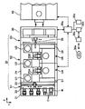
- FIG. 1 is a perspective view schematically showing an interface apparatus according to an embodiment of the present invention, and a resist coating and developing apparatus and an EUV exposure apparatus suitable for applying the interface apparatus. It is a top view which shows schematically the interface apparatus of FIG. 1, a resist coating and developing apparatus, and EUV exposure apparatus.
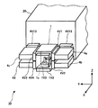
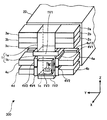
- 1 is a perspective view schematically showing an interface device according to an embodiment of the present invention.
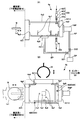
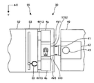
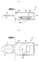
- FIG. 4 is a cross-sectional view (A) and a plan view (B) schematically showing a load lock chamber of the interface device shown in FIG. 3. It is a top view which expands and shows the positional relationship of the interface apparatus by embodiment of this invention, and the resist coating and developing apparatus suitable for applying this, and EUV exposure apparatus.
- An interface apparatus is applied in a resist coating and developing apparatus (hereinafter simply referred to as a coating and developing apparatus) that applies a resist film to a wafer W and develops the exposed resist film, and a coating and developing apparatus. It is provided between the EUV exposure apparatus that exposes the resist film with EUV light.
- a coating and developing apparatus that applies a resist film to a wafer W and develops the exposed resist film
- the coating and developing apparatus 20 has a cassette station S1 for loading and unloading a wafer W accommodated in a wafer cassette C such as a so-called FOUP (Front-Opening-Universal-Pod).
- the cassette station S1 includes a mounting table 21 on which a plurality of wafer cassettes C can be mounted, a plurality of opening / closing sections 22 provided corresponding to the plurality of wafer cassettes C mounted on the mounting table 21, and a wafer cassette opening / closing operation.
- a transfer mechanism 23 (FIG. 2) that takes the wafer W out of the wafer cassette C and returns it to the wafer cassette C.
- the wafer cassette C can store a plurality of (for example, 13) wafers W.
- the coating and developing apparatus 20 has a processing unit S2 surrounded by a casing 24 next to the cassette station S1.
- the processing unit S2 the shelf unit U1, the main transport unit 25A, the shelf unit U2, the main transport unit 25B, and the shelf unit U3 are arranged in this order along the X direction.
- Each of the shelf units U1, U2, and U3 includes a multi-stage (eg, 10-stage) heating unit and / or cooling unit for performing pre-processing and post-processing for processing performed in the liquid processing units U4 and U5 (described later).
- a multi-stage heating unit and / or cooling unit for performing pre-processing and post-processing for processing performed in the liquid processing units U4 and U5 (described later).
- the main transfer units 25A and 25B transfer the wafer W between various processing units including the shelf units U1, U2, and U3 and the coating / developing units U4 and U5.
- Each of the shelf units U1, U2, U3 and the main transfer portions 25A, 25B has an opening (not shown), and the wafer W can be transferred from the shelf unit U1 to the shelf unit U3 through the openings.
- the transport unit 25A is arranged so as to be surrounded by the shelf unit U1, the liquid processing unit U4, and the shelf unit U2.
- the transport unit 25B is disposed so as to be surrounded by the shelf unit U2, the liquid processing unit U5, and the shelf unit U3.
- the liquid processing units U4 and U5 are arranged on the storage unit 29 for storing a resist solution and a developer, and the coating unit COT, the development unit DEV, and the antireflection film are formed.
- the liquid processing unit U4 has a three-stage coating unit COT and a two-stage antireflection film forming unit BARC, and the liquid processing unit U5 has a five-stage developing unit DEV.
- the combination of the developing unit DEV and the antireflection film forming unit BARC is not limited to the illustrated example, and may be appropriately combined.
- a temperature / humidity adjustment unit 27 (28) including a temperature adjustment device for liquid used in the liquid treatment unit, a duct used for temperature / humidity adjustment, and the like is provided. Yes.
- the transfer unit S3 includes a transfer unit 33 that transfers the wafer W between the processing unit S2 and an interface device 30 (300) according to an embodiment of the present invention described later.
- the delivery unit 33 has a support part that supports and conveys the outer peripheral part of the back surface of the wafer W.
- the support part can move in the Y-axis direction in FIG. 2 and can rotate around the base end. it can.
- the wafer W can be delivered between the processing unit S2 and the interface device 30.
- an interface device 30 (or 300) according to an embodiment of the present invention is disposed adjacent to the transport unit S3 of the coating and developing apparatus 20, and the EUV exposure apparatus is adjacent to the interface device 30. 40 is arranged. That is, the interface device 30 is disposed between the coating and developing device 20 and the EUV exposure device 40.
- the EUV exposure apparatus 40 includes a vacuum chamber 42 having a transfer port (not shown) provided with a gate valve 41, and a wafer that is disposed in the vacuum chamber 42 and is subject to exposure processing. And a wafer stage 43 to be placed.
- a transfer port not shown
- a wafer stage 43 to be placed in the vacuum chamber 42.
- an optical system including a multilayer mirror is arranged, and the EUV light from an EUV light source (not shown) arranged outside the vacuum chamber 42 is used on the wafer stage 43. The wafer is exposed.
- FIG. 3 is a perspective view of the configuration of the interface device 30 as viewed from the EUV exposure apparatus 40 (not shown).
- the interface device 30 includes a cabinet having substantially the same height and width as the coating and developing device 20 (conveyance unit S3), but is omitted in FIG.
- the interface device 30 has a transfer chamber 1 in a substantially central portion.
- the interface device 30 includes a load lock chamber 4a connected to the transfer chamber 1 via the gate valve 4V1, and a load connected to the transfer chamber 1 via the gate valve 4V2 and arranged below the load lock chamber 4a.
- the lock chamber 4b is connected to the transfer chamber 1 via the gate valve 4V3, and is connected to the transfer chamber 1 via the gate valve 4V4 and the load lock chamber 4c facing the load lock chamber 4a with the transfer chamber 1 in between. And a load lock chamber 4d disposed below the load lock chamber 4c.
- a turbo molecular pump (not shown) is connected to the transfer chamber 1 via a gate valve 1V2.
- the transfer chamber 1 has a transfer port (not shown) that opens toward the EUV exposure apparatus 40, and this transfer port is opened and closed by a gate valve 1V3.
- the wafer W is carried in and out between the interface apparatus 30 and the EUV exposure apparatus 40 through this conveyance port.
- the gate valves 1V2, 1V3 and the gate valves 4V1 to 4V4 are closed, the transfer chamber 1 is sealed.
- the gate valve 1V2 is opened and evacuated by the turbo molecular pump, the inside of the transfer chamber 1 is 10 ⁇ 4 to 10 ⁇ 5. It is maintained at a reduced pressure of about Pa.
- the pressure in the transfer chamber 1 can be measured with a vacuum gauge (not shown).
- the vacuum gauge may be a general ion gauge. However, since the resist film formed on the wafer W may be deteriorated by light or electrons emitted from the ion gauge, the ion gauge is in a position where the light or electrons from the ion gauge do not reach the resist film.
- a vacuum gauge can also be provided in the load lock chambers 4a to 4d. Also in this case, the ion gauge as a vacuum gauge is provided at a position where light and electrons from the ion gauge do not reach the resist film.
- a wafer transfer unit 1 c is provided in the transfer chamber 1.
- the wafer transfer unit 1c can be expanded and contracted in the vertical direction (Z-axis direction in FIG. 3), and can be rotated about 360 ° about the vertical direction as a central axis.
- the wafer transfer unit 1c has two wafer support plates 1c1 (only one is shown in FIG. 4) that holds the back surface of the wafer W at the tip, and the wafer support plates 1c1 are arranged along the X direction and the Y direction. Can be moved.
- the two wafer support plates 1c1 are configured to be alternately advanced and retracted, and can handle two wafers W at a time.
- the wafer support plate 1c1 may have a cooling function or a temperature control function.
- FIG. 4A is a schematic cross-sectional view of the load lock chamber 4a
- FIG. 4B is a schematic top view of the load lock chamber 4a.
- the load lock chamber 4a has a flat housing 4a2.
- the housing 4a2 includes a transport port 4a3 that can be opened and closed by a gate valve 4V1, an exhaust port 4a4 that can be opened and closed by a gate valve 4V11, and a high vacuum exhaust port that can be opened and closed by a gate valve 4V12. 4a5.
- the housing 4a2 has a transport port 4a6 that can be opened and closed by a gate valve 4V13.
- the transfer port 4a3 is formed on a side wall facing the transfer chamber 1 in the housing 4a2. Through the transfer port 4a3, the wafer W is transferred between the transfer chamber 1 and the housing 4a2 by the wafer support plate 1c1.
- the transport port 4a6 is formed on the side wall facing the coating and developing apparatus 20 in the housing 4a2. The wafer W is carried in and out between the coating and developing apparatus 20 and the housing 4a2 by the transfer unit 33 provided in the transport unit section S3 of the coating and developing apparatus 20 through the transport port 4a6.
- the exhaust port 4a4 is used when the inside of the housing 4a2 is roughly exhausted.
- a bypass pipe BP is connected to the gate valve 4V11 provided at the exhaust port 4a4, and the bypass pipe BP is connected to the dry pump DP.
- a stop valve SV1 is provided in the middle of the bypass pipe BP. With this configuration, the inside of the load lock chamber 4a can be roughly exhausted.
- the high vacuum exhaust port 4a5 is used when the inside of the housing 4a2 is high vacuum exhausted.
- a turbo molecular pump TMP is connected to the gate valve 4aV12 provided in the high vacuum exhaust port 4a5, an auxiliary exhaust pipe AP is connected to the turbo molecular pump TMP, and a dry pump DP is connected to the auxiliary exhaust pipe AP.
- a stop valve SV2 is provided in the middle of the auxiliary exhaust pipe AP.
- the roughly evacuated load lock chamber 4a can be evacuated to a high vacuum (eg, 10 ⁇ 4 to 10 ⁇ 5 Pa).
- the dry pump DP functions as a rough exhaust pump in the load lock chamber 4a and an auxiliary pump for the turbo molecular pump TMP by switching the stop valves SV1 and SV2.
- the wafer support pins 4a7 for supporting the wafer W are provided.
- the wafer support pins 4a7 do not move up and down. Therefore, the wafer W is placed on the wafer support pins 4a7 by the wafer support plate 1c1 and the transfer unit 33 moving up and down, and from the wafer support pins 4a7. Be taken up.
- the wafer support pins 4a7 may be provided to be movable up and down.
- the housing 4a2 is provided with a set of gas blowers 400.
- one gas blower 400 is disposed on the ceiling and bottom of the housing 4a2 at a position away from the transfer port 4a3 in the housing 4a2, and the other gas blower 400 is disposed.
- they are arranged on the ceiling and bottom of the housing 4a2 at a position away from the transport port 4a6.
- the gas blower 400 has a gas line provided in the middle of a pipe 401 and a pipe 401 inserted in a through hole provided in a ceiling portion of the casing 4a2 at one end.
- the other end of the pipe 401 is connected to a gas supply source (not shown).
- the gas supply source includes, for example, a nitrogen (N 2 ) gas cylinder, so that N 2 gas can be supplied from the gas supply source to the pipe 401. Further, the gas supply source may be configured to supply dry air to the pipe 401.
- the gas line filter 402 includes, for example, a filter membrane made of a fluororesin, and removes foreign matters in the N 2 gas flowing in the pipe 401. As shown in FIG.
- the gas ejection slit 404 extends in a direction intersecting with the loading / unloading direction of the wafer W.
- N 2 gas can be ejected from the gas ejection slit 404.
- the slit width of the gas ejection slit 404 is set such that a pressure difference that causes, for example, an air curtain to be formed by the gas ejected from the gas ejection slit 404 inside and outside the pipe 401.
- a gas inlet 4a8 is formed at the bottom of the housing 4a2, and a pipe (not shown) connected to the gas inlet 4a8 has a stop valve and a safety valve to prevent the the casing 4a2 is pressurized is provided with (not both shown), by opening the stop valve, for example, N 2 gas or dry air flows into the casing 4a2.
- the stop valve for example, N 2 gas or dry air flows into the casing 4a2.
- this N 2 gas flows from the casing 4a2 into the coating and developing apparatus 20 through the transport port 4a6, the inflow of air from the coating and developing apparatus 20 into the casing 4a2 can be reduced.
- the inside of the coating and developing apparatus 20 is under atmospheric pressure and is filled with air in a clean room.
- the air in the clean room contains organic matter, but it is possible to reduce the inflow of organic matter into the housing 4a2 by continuing to flow the N 2 gas in this way.
- moisture in the air adheres to the inner wall of the housing 4a2, and it takes a long time to exhaust to high vacuum.
- the form of the load lock chamber 4a since the inflow of air from the coating and developing apparatus 20 can be reduced by the N 2 gas from the gas inlet 4a8, the time until exhausting to high vacuum can be shortened. .
- the load lock chamber 4a has been described above, but the load lock chambers 4b to 4d have the same configuration.
- the turbo molecular pump TMP is provided for each of the load lock chambers 4a to 4d, while the dry pump DP can be commonly used as an auxiliary pump and a rough exhaust pump for all of the load lock chambers 4a to 4d.
- the load lock chamber 4b is roughly evacuated from the atmospheric pressure while the load lock chamber 4a is being evacuated to high vacuum, the pressure in the bypass pipe BP and the auxiliary exhaust pipe AP temporarily rises, but the turbo molecular pump TMP Therefore, the pressure in the load lock chamber 4a does not increase, and a high vacuum is maintained.
- the interface device 30 is connected to the control unit 30a that controls the load lock chamber, the module, the gate valve, the pump, various devices, etc. that constitute the interface device 30, and is connected to a predetermined unit.
- a storage device 30b for storing the program, an input / output (I / O) device 30c for reading the program stored in the computer-readable storage medium 30e into the storage device 30b, and the control unit 30a are connected to change the process parameters. It has a display device 30d for displaying a process recipe for updating and displaying a process status.
- the control unit 30a may be, for example, a computer including a CPU (Central Processing Unit) as a component, and each of the interface devices 30 is based on a program having a command group for causing the interface device 30 to execute, for example, a process described later. Operate the equipment and carry out the process.
- This program may be stored in various computer-readable recording media 30e including a hard disk, an optical disk, a magnetic disk, and a semiconductor memory device, read through the I / O device 30c, and stored in the storage device 30b. Are read out and executed by the control unit 30a.
- the control unit 30a is connected to the control unit (not shown) of the coating and developing apparatus 20 and the EUV exposure apparatus 40, and between the coating and developing apparatus 20 and the control unit of the EUV exposure apparatus 40 according to the above program. Signals are transmitted and received (broken line arrows in FIG. 2), and processes by the coating and developing apparatus 20, the interface apparatus 30, and the EUV exposure apparatus 40 are executed. Thereby, for example, the transfer unit 33 of the coating and developing apparatus 20 and the load lock chamber 4a of the interface device 30 cooperate to transfer the wafer W from the transfer unit 33 to the load lock chamber 4a.
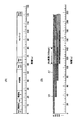
- FIG. 6 is merely an example of a time chart for wafer conveyance, and does not limit the present invention.
- the wafer cassette C in which the wafers W are stored is mounted on the mounting table 21.
- the lid of the wafer cassette C is removed, the opening / closing part 22 corresponding to the wafer cassette C is opened, and the wafer W is taken out from the wafer cassette C by the transfer mechanism 23 (FIG. 2).
- the wafer W is delivered to the main transfer unit 25A via a delivery unit (not shown) that forms one stage of the shelf unit U1.
- the wafer W is transferred to one of the shelves U1 to U2 by the main transfer unit 25A, subjected to, for example, a hydrophobizing process or a cooling process as a pre-process, and further transferred to the coating unit COT, where The film is spin coated.
- the wafer W is transferred to a heating unit on any one of the shelf units U1 to U3, and prebaked.
- the wafer W is transferred from the shelf unit U3 to the transfer unit 33 (FIG. 5) of the transfer unit unit S3.
- the delivery unit 33 moves in front of the gate valve 4V13 of the load lock chamber 4a while supporting the wafer W.
- the inside of the load lock chamber 4a is at atmospheric pressure by the N 2 gas supplied from the gas inlet 4a8, that is, the gate valve 4V13 is ready to be opened.
- the gate valve 4V13 is opened, the delivery unit 33 enters the housing 4a2 of the load lock chamber 4a. At this time, by continuing to supply N 2 from the gas inlet 4a8, the inflow of air from the transport unit S3 into the housing 4a2 can be reduced.
- the inflow of air into the housing 4a2 can be further reduced.
- the wafer W transferred into the housing 4a2 is supported by the wafer support pins 4a7 as the transfer unit 33 moves downward. After the delivery unit 33 is withdrawn from the housing 4a2, the gate valve 4V13 is closed, and the transfer of the wafer W to the load lock chamber 4a is completed.
- the time required to carry the wafer W into the load lock chamber 4a (the time from when the gate valve 4V13 is opened until it is closed again) can be, for example, about 6 seconds (“waf. In1” in FIG. 6).
- the gate valve 4V11 is opened, and the inside of the housing 4a2 is roughly evacuated.
- the rough exhaust time may be, for example, about 9 seconds (“rough exhaust 1” in FIG. 6).
- the gate valve 4V11 is closed to stop the exhaust, and for example, N 2 gas is supplied from the gas inlet 4a8, and the inside of the housing 4a2 is returned to the atmospheric pressure in about 4 seconds (“N2” in FIG. 6).
- the supply of N 2 gas from the gas inlet 4a8 is stopped, and the rough exhaust is performed again by opening the gate valve 4V11.
- This rough exhaust may be performed for about 9 seconds (“rough exhaust 2” in FIG. 6).
- the gate valve 4V11 is closed to stop the rough exhaust, and the gate valve 4V12 is opened, and the inside of the housing 4a2 is evacuated by the turbo molecular pump TMP.
- the high vacuum evacuation may be about 26 seconds (“main evacuation” in FIG. 6). Even if air slightly flows into the housing 4a2 of the load lock chamber 4a when the wafer W is loaded, it can be purged by high vacuum evacuation in addition to two rough evacuations.
- the transfer chamber 1 is also evacuated by a turbo molecular pump (not shown) with the gate valve 1V2 opened.
- the gate valve 4V12 of the load lock chamber 4a and the gate valve 1V2 of the transfer chamber 1 are closed, and the load lock chamber 4a and the transfer chamber 1 are The gate valve 4V1 is opened.
- the wafer support plate 1c1 of the wafer transfer unit 1c in the transfer chamber 1 enters the load lock chamber 4a, lifts the wafer W on the wafer support pins 4a7, and carries it out to the transfer chamber 1.
- the gate valve 1V3 of the transfer chamber 1 and the gate valve 41 (FIG. 5) of the EUV exposure apparatus 40 are opened, and the wafer W is transferred into the vacuum chamber 42 of the EUV exposure apparatus 40 by the wafer transfer unit 1c. Is mounted on the wafer stage 43.
- the wafer W is transferred to a predetermined load lock chamber in accordance with a predetermined transfer flow indicating how one wafer W is transferred. Specifically, according to the transport flow, the material is transported to the load lock chamber where high vacuum evacuation has been completed at this point.
- the gate valve 4V1 is first opened, and the wafer transfer unit 1c carries the exposed wafer W into the load lock chamber 4a and places it on the wafer support pins 4a7.
- the gate valve 4V1 is closed. It takes, for example, about 7 seconds until the gate valve 4V1 is opened and closed (“waf. In2” in FIG. 6).
- N 2 gas flows into the load lock chamber 4a from the gas inlet 4a8, and the load lock chamber 4a is returned to the atmospheric pressure, for example, over about 50 seconds (“N 2 purge” in FIG. 6). .
- the gate valve 4V13 is opened with the N 2 gas flowing from the gas inlet 4a8.
- the load lock chamber 4a and the transport unit portion S3 of the coating and developing apparatus 20 communicate with each other through the transport port 4a6 (FIG. 4B).
- the N 2 gas heading from the load lock chamber 4a toward the transfer unit unit S3 reduces the inflow of air from the transfer unit unit S3, and the inside of the load lock chamber 4a is maintained in a clean atmosphere.
- the transfer unit 33 of the transfer unit unit S3 enters the load lock chamber 4a, receives the wafer W on the wafer support pins 4a7, and exits to the transfer unit unit S3. Thereafter, the gate valve 4V13 is closed, and the transfer of the wafer W to the coating and developing apparatus 20 is completed.
- the time required to transfer the wafer W from the load lock chamber 4a to the transfer unit S3 can be, for example, about 5 seconds (“waf. Out2” in FIG. 6A).
- the gate valve 4V13 may be closed after the next wafer W is loaded into the load lock chamber 4a.
- the exposed wafer W is transferred to the developing unit DEV by the main transfer unit 25B (FIG. 2), and the resist film on the wafer W is developed by the developing unit DEV to form a resist mask. Thereafter, the wafer W is returned to the original wafer cassette C on the mounting table 21 by the main transfer unit 25A and the transfer mechanism 23 (FIG. 2).
- the procedure for transporting one wafer has been described.
- a plurality of wafers W1, W2, W3, W4,... As shown in FIG. 5B, for example, when the preceding wafer W1 is in the load lock chamber 4a and the inside of the load lock chamber 4a is being evacuated to a high vacuum, the next wafer W2 is transferred to the load lock chamber 4b. The conveyance may be started. Further, when the wafer W2 is in the load lock chamber 4b and the inside of the load lock chamber 4b is evacuated to a high vacuum, the transfer of the next wafer W3 to the load lock chamber 4c may be started.
- the wafer support plate 1c1 that does not support the wafer W enters the load lock chamber 4a, and the load lock The wafer W in the chamber 4a is received and moved out into the transfer chamber 1.
- the wafer W in the load lock chamber 4a is transferred to the transfer chamber 1 (“waf.1in1” in FIG. 6A).
- the wafer transfer unit 1c transfers the wafer W unloaded from the EUV exposure apparatus 40 into the load lock chamber 4a by the wafer support plate 1c1 and places it on the wafer support pins 4a7 in the load lock chamber 4a.
- the exposed wafer W is carried into the load lock chamber 4a ("waf. In2" in FIG. 6A).
- the gate valve 4V1 is closed.
- the time required from when the gate valve 4V1 is opened until it is closed again can be, for example, about 15 seconds (“waf. In1” + “waf. In2” in FIG. 6A).
- wafer loading / unloading is possible not only between the transfer chamber 1 and the load lock chambers 4a to 4d but also between the transfer chamber 1 and the vacuum chamber 42 in the EUV exposure apparatus 40.
- the throughput can be improved. That is, according to the above description, the time for which one wafer W exists in the interface device 30 (the total time in the time chart of FIG. 6A) is about 124 seconds, but after 124 seconds, the next wafer W Instead of starting the transfer, the wafers W can be transferred sequentially with a predetermined time difference.
- the transfer of the wafers W may be started about every 36 seconds as shown in FIG. 6B. In this case, about 144 seconds are allowed for the exposure processing of one wafer W.
- rough evacuation can be performed three times or the time of high vacuum evacuation (main exhaust) can be increased, and organic substances in the air can be further prevented from entering the EUV exposure apparatus 40. It becomes possible.
- the period during which the load lock chambers 4a to 4d are at atmospheric pressure (“N2 purge”, “waf. In2”, and “waf. In1” will be described according to the reference numerals in FIG. 6A). ”Is indicated by a symbol“ AT ”, and a period during which pressure is reduced (including“ N2 ”after“ rough exhaust 1 ”) is indicated by a symbol“ VA ”.
- the interface device 30 includes the plurality of load lock chambers 4a to 4d, and can continuously transfer the wafer W in a sheet form.
- the interface device 30 Through the rough exhaust of the lock chambers 4a to 4d, the atmospheric filling of the clean gas, the rough exhaust again, and the high vacuum exhaust, it is possible to improve the throughput while reducing the contamination caused by the organic matter in the air.
- the time from resist application to exposure and the time from exposure to development can be made substantially the same for each wafer W, so that variations in process reproducibility between wafers can be minimized. .
- N 2 gas from the gas inlet 4a8 of the load lock chamber 4a
- the load lock chambers 4a to 4d have the same configuration and are unitized, for example, if the gate valve 4V1 and the stop valves SV1 and SV2 of the load lock chamber 4a are closed, the load lock chambers 4b to 4d are closed. It is possible to remove the casing 4a2 of the load lock chamber 4a from the gate valve 4V1 and perform maintenance of the load lock chamber 4a while performing the process using the.
- the interface apparatus according to the second embodiment is disposed between the coating and developing apparatus 20 and the EUV exposure apparatus 40 in the same manner as the interface apparatus 30 according to the first embodiment.
- the interface device 300 according to the second embodiment is compared with the interface device 30 according to the first embodiment by a gate valve 1 ⁇ / b> V ⁇ b> 1 provided at a substantially middle portion in the vertical direction of the transfer chamber 1.
- the transfer chamber 1 is divided into an upper transfer chamber 1a and a lower transfer chamber 1b, and a plurality of load lock chambers 4a to 4d are connected to the lower transfer chamber 1b via corresponding gate valves 4V1 to 4V4, and communicate with the upper transfer chamber 1a.
- the heating modules 2a to 2c and the cooling modules 3a to 3c are different, and the other points are the same.
- the interface device 300 according to the present embodiment will be described focusing on the differences while omitting the redundant description regarding the configuration of the load lock chambers 4a to 4d.
- the interface device 300 has a transfer chamber 1 that extends in the vertical direction at the center, and the transfer chamber 1 is transported by an upper transfer by a gate valve 1V1 provided in a substantially middle portion in the vertical direction. It is divided into a chamber 1a and a lower transfer chamber 1b.
- the interface device 300 is arranged in a multi-tiered manner on the right side ( ⁇ Y side) of the upper transfer chamber 1a above the load lock chamber 4a, and is connected to the three heating modules 2a, 2b communicating with the upper transfer chamber 1a. 2c and three cooling modules 3a, 3b, 3c arranged in multiple stages on the left side (+ Y side) of the upper transfer chamber 1a above the load lock chamber 4c and communicating with the upper transfer chamber 1a.
- the upper transfer chamber 1a can be evacuated by, for example, a dry pump or the like (not shown) and maintained in a reduced pressure state of 10 ⁇ 2 to 10 ⁇ 4 Pa.
- a stop valve, a check valve, a pressure adjustment valve, and the like are provided on the pipe connecting the upper transfer chamber 1a and the dry pump.
- the pressure in the upper transfer chamber 1a can be measured with a vacuum gauge (not shown).
- the vacuum gauge may be a general ion gauge. However, since the resist film formed on the wafer W may be deteriorated by light or electrons emitted from the ion gauge, the ion gauge is in a position where the light or electrons from the ion gauge do not reach the resist film.
- Vacuum gauges can also be provided in the load lock chambers 4a to 4d, the lower transfer chamber 1b, the heating modules 2a, 2b, and 2c, and the cooling modules 3a, 3b, and 3c. Also in this case, the ion gauge as a vacuum gauge is provided at a position where light and electrons from the ion gauge do not reach the resist film.
- a turbo molecular pump (not shown) is connected to the lower transfer chamber 1b via a gate valve 1V2.
- the lower transfer chamber 1b has a transfer port (not shown) that opens toward the EUV exposure apparatus 40 and can be closed by the gate valve 1V3. Through this transfer port, the wafer W is transferred between the interface apparatus 300 and the EUV exposure apparatus 40.
- the gate valves 1V1 to 1V3 and the gate valves 4V1 to 4V4 are closed, the lower transfer chamber 1b is hermetically sealed, while the gate valve 1V2 is opened and evacuated by a turbo molecular pump. A reduced pressure of about 10 ⁇ 4 to 10 ⁇ 5 Pa is maintained.
- a wafer transfer unit 1c is provided in the lower transfer chamber 1b.
- the wafer transfer unit 1c can be expanded and contracted in the vertical direction (Z direction in FIG. 7), and can be rotated about the vertical direction as a central axis.
- the wafer transfer unit 1c has two wafer support plates 1c1 (only one is shown in FIGS. 8 and 9) for holding the back surface of the wafer W at the tip, and the wafer support plate 1c1 is arranged in the X direction and the Y direction. Can be moved along.
- the two wafer support plates 1c1 each have a fluid conduit, and the temperature can be adjusted by, for example, flowing a fluid to the fluid conduit through a flexible pipe.
- the heated wafer W is removed by the wafer support plate 1c1 when the wafer W is taken out from the heating modules 2a to 2c. It can be cooled to a certain temperature (so-called rough heat can be taken). Therefore, the heated wafer W can be quickly cooled, and the cooling in the cooling modules 3a to 3c can be performed more efficiently.
- the two wafer support plates 1c1 are configured to be alternately advanced and retracted, and can handle two wafers W at a time.
- the wafer transfer unit 1c allows the wafer support plate 1c1 to enter the load lock chamber 4a (4a to 4d) and the load lock chamber 4a (4a to 4d).
- the wafer W can be taken out, and the wafer W can be loaded into the load lock chamber 4a (4a to 4d).
- the wafer transfer unit 1c extends in the Z direction and can enter the upper transfer chamber 1a. From the upper transfer chamber 1a, the heating module 2a to 2c or the cooling module 3a to The wafer support plate 1c1 can be made to enter 3c. That is, the wafer transfer unit 1c can access not only the load lock chambers 4a to 4d but also the heating modules 2a to 2c and the cooling modules 3a to 3c.
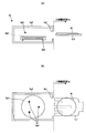
- the heating module 2a is arranged in a flat housing 2a2 having an opening 2a1 that opens toward the upper transfer chamber 1a, and the housing 2a2. It has a mounting table 2a3 on which a wafer W transferred from the upper transfer chamber 1a is mounted by a wafer transfer unit 1c (wafer support plate 1c1).
- the mounting table 2a3 has a thermoelectric heater and a thermocouple (both not shown) inside, and is maintained at a predetermined temperature by these and a predetermined temperature controller (not shown). Thereby, the wafer W on the mounting table 2a3 can be heated.
- the mounting table 2a3 is provided with three elevating pins 2a4 that can move up and down through the through holes provided in the mounting table 2a3.
- the elevating pins 2a4 receive the wafer W supported above the mounting table 2a3 by the wafer support plate 1c1, place the wafer W on the mounting table 2a3, and lift the wafer W on the mounting table 2a3 to raise the wafer support plate 1c1. Wafer W can be delivered to
- the mounting table 2a3 is provided with an electrostatic chuck 2a5.
- a predetermined voltage is applied to the electrostatic chuck 2a5 from a power source (not shown)
- the wafer W placed on the mounting table 2a3 is brought into close contact with the upper surface of the mounting table 2a3 by electrostatic force.
- the wafer W can be heated efficiently.
- the inside of the heating module 2a is maintained at a reduced pressure similarly to the upper transfer chamber 1a through the opening 2a1 and heat conduction due to retention is less likely to occur, the wafer W is placed on the upper surface of the mounting table 2a3 by the electrostatic chuck 2a5.
- the effect of adhering is great.
- the heating modules 2b and 2c have the same configuration as the heating module 2a.
- the cooling module 3a is disposed in a flat housing 3a2 having an opening 3a1 opening toward the upper transfer chamber 1a, and the housing 3a2. It has a mounting table 3a3 on which a wafer W carried from the upper transfer chamber 1a by the wafer transfer unit 1c is mounted. As shown in FIG. 9A, a conduit 3a4 is formed inside the mounting table 3a3, and a predetermined fluid whose temperature is adjusted into the conduit 3a4 from a fluid circulator (not shown) having a temperature control function. As a result, the mounting table 3a3 is maintained at a predetermined temperature. Thereby, the wafer W on the mounting table 3a3 can be cooled.
- the mounting table 3a3 is provided with three lifting pins 3a4 (FIG. 9B) that can project and retract the wafer W with respect to the upper surface of the mounting table 3a3.
- the mounting table 3a3 is provided with an electrostatic chuck 3a5 (FIG. 9A), and the wafer W mounted on the mounting table 3a3 by the lifting pins 3a4 is placed on the upper surface of the mounting table 3a3 by the electrostatic chuck 3a5. It is closely attached to. Thereby, heat conduction between the wafer W and the mounting table 3a3 is promoted.
- the cooling modules 3b and 3c also have the same configuration as the cooling module 3a.
- the wafer cassette C in which the wafers W are stored is mounted on the mounting table 21.
- the lid of the wafer cassette C is removed, the opening / closing part 22 corresponding to the wafer cassette C is opened, and the wafer W is taken out from the wafer cassette C by the transfer mechanism 23 (FIG. 2).
- the wafer W is delivered to the main transfer unit 25A via a delivery unit (not shown) that forms one stage of the shelf unit U1.
- the wafer W is transferred to one of the shelves U1 to U2 by the main transfer unit 25A, subjected to, for example, a hydrophobizing process or a cooling process as a pre-process, and further transferred to the coating unit COT, where The film is spin coated.
- the wafer W is delivered to the delivery unit 33 of the transfer unit unit S3 via the shelf unit U3.
- the delivery unit 33 moves in front of the gate valve 4V13 of the load lock chamber 4a while supporting the wafer W (see FIG. 5).
- the inside of the load lock chamber 4a is at atmospheric pressure by N 2 gas supplied from the gas inlet 4a8.
- the gate valve 4V13 is opened, the delivery unit 33 enters the housing 4a2 of the load lock chamber 4a.
- N 2 from the gas inlet 4a8
- the inflow of air into the housing 4a2 can be further reduced.
- the wafer W transferred into the housing 4a2 is supported by the wafer support pins 4a7 as the transfer unit 33 moves downward.
- the lower transfer chamber 1b in which the wafer W is transferred next is also evacuated to a predetermined pressure, and preparations for receiving the wafer W are completed.
- the gate valve 4V1 between the load lock chamber 4a and the lower transfer chamber 1b is opened, and a wafer transfer unit provided in the lower transfer chamber 1b.
- the wafer support plate 1c1 of 1c enters the housing 4a2 and receives the wafer W.
- the gate valve 4V1 is closed.
- the upper transfer chamber 1a to which the wafer W is transferred next is also maintained at a predetermined pressure.
- the gate valve 1V1 FIG. 7 between the lower transfer chamber 1b and the upper transfer chamber 1a is opened, the wafer transfer unit 1c extends upward and enters the upper transfer chamber 1a, and the opening of the heating module 2a.
- the wafer W is transferred into the housing 2a2 of the heating module 2a through 2a1.
- the wafer W is received by the lift pins 2a4 and placed on the placement table 2a3. Then, the wafer W is brought into close contact with the upper surface of the mounting table 2a3 by the electrostatic chuck 2a5.
- the mounting table 2a3 is maintained at a predetermined temperature, whereby the wafer W coated with the resist film is heated (pre-baked).
- the prebaking temperature can be, for example, about 80 to about 150 ° C.
- the prebaking time can be, for example, about 30 to about 120 seconds.
- the inside of the housing 2a2 of the heating module 2a is maintained at a predetermined pressure (reduced pressure) similarly to the upper transfer chamber 1a, so outgas from the resist film on the wafer W is promoted, and the wafer W Outgas in the vacuum chamber 42 in the EUV exposure apparatus 40 to be transported later is reduced. Thereby, it is possible to reduce the contamination of the optical system due to the solvent or the like in the resist film.
- the same procedure is sequentially started for the second and subsequent wafers, and the second wafer is heated from the load lock chamber 4b through the lower transfer chamber 1b and the upper transfer chamber 1a, for example. 2b, where pre-baking is performed. Further, the third wafer is transferred from the load lock chamber 4c to the heating module 2c through the lower transfer chamber 1b and the upper transfer chamber 1a, for example, and the fourth wafer is transferred to the load lock chamber 4d, for example. Is done.
- the wafer transfer unit 1c transfers the wafer W from the heating module 2a to the cooling plate 3a.
- the cooling starts immediately when the wafer W is received by the wafer support plate 1c1. Therefore, when the wafer W is transferred to the cooling plate 3a and placed on the mounting table 3a3, the wafer W is cooled to a certain temperature, and the cooling module 3a can be efficiently cooled. In the cooling module 3a, the wafer W is cooled to a temperature of about room temperature (about 22 ° C.).
- the wafers W in the heating modules 2b and 2c are also transferred to the cooling modules 3b and 3c, respectively, and the wafers W in the load lock chambers 4a to 4d are sequentially transferred to the heating modules 2a to 2c.
- the wafer W is transferred by the wafer transfer unit 1c through the upper transfer chamber 1a to the lower transfer chamber 1b. Then, after the gate valve 1V1 between the upper transfer chamber 1a and the lower transfer chamber 1b is closed, the gate valve 1V2 is opened and the lower transfer chamber 1b is evacuated to high vacuum.
- the gate valve 1V3 provided in the lower transfer chamber 1b and the gate valve 41 of the EUV exposure apparatus 40 are opened, and the wafer W is subjected to EUV exposure by the wafer transfer unit 1c. It is transferred into the vacuum chamber 42 of the apparatus 40 and placed on the wafer stage 43 (see FIG. 5).
- the gate valve 1V1 between the upper transfer chamber 1a and the lower transfer chamber 1b is open, and the pressure in the lower transfer chamber 1b is realized by a dry pump.
- the gate valve 1V1 is closed at a predetermined timing, and high vacuum evacuation is performed through the gate valve 1V2. Thereby, the inside of the vacuum chamber 42 in the EUV exposure apparatus 40 can be maintained at a high vacuum.
- the wafer W returned to the lower transfer chamber 1b is transferred to a predetermined heating module (for convenience, referred to as the heating module 2a) according to a predetermined transfer flow for post-exposure baking.
- the gate valve 1V1 is opened, the wafer transfer unit 1c extends upward, enters the upper transfer chamber 1a, and transfers the wafer W into the housing 2a2 of the heating module 2a through the opening 2a1 of the heating module 2a.
- the wafer W is mounted on the mounting table 2a3 by the lift pins 2a4.
- the wafer W is brought into close contact with the upper surface of the mounting table 2a3 by the electrostatic chuck 2a5.
- the cooling module to be transferred is determined according to a predetermined transfer flow (for convenience, it is transferred to the cooling module 3a). Also in this case, when the wafer W heated by the heating module 2a is received by the wafer support plate 1c1, it is cooled to a certain temperature by the wafer support plate 1c1.
- the wafer W is transferred from the cooling module 3a through the upper transfer chamber 1a to the lower transfer chamber 1b by the wafer transfer unit 1c.
- the wafer W is transferred to a predetermined load lock chamber (for convenience, the load lock chamber 4a) according to the transfer flow. That is, when the gate valve 1V1 is first closed and then the gate valve 4V1 is opened, the wafer W is transferred into the load lock chamber 4a by the transfer unit 1c and placed on the wafer support pins 4a7 in the load lock chamber 4a. .
- the gate valve 4V1 is closed and, for example, N 2 gas flows into the load lock chamber 4a from the gas inlet 4a8. Becomes atmospheric pressure. Thereafter, the gate valve 4V13 is opened with the N 2 gas flowing from the gas inlet 4a8. As a result, the load lock chamber 4a and the transport unit S3 of the coating and developing apparatus 20 communicate with each other via the transport port 4a6 (see FIG. 4B). Further, the N 2 gas flowing from the load lock chamber 4a to the transfer unit portion S3 reduces the inflow of air from the transfer unit portion S3, and the inside of the load lock chamber 4a is maintained in a clean atmosphere.
- the transfer unit 33 of the transfer unit unit S3 enters the load lock chamber 4a, receives the wafer W on the wafer support pins 4a7, and exits to the transfer unit unit S3. Thereafter, the gate valve 4V13 is closed, and the transfer of the wafer W to the coating and developing apparatus 20 is completed.
- the film is transferred to the developing unit DEV by the main transfer unit 25B (FIG. 2), and the resist film on the wafer W is developed by the developing unit DEV to form a resist mask. Thereafter, the wafer W is returned to the original wafer cassette C on the mounting table 21.
- the interface device 300 includes the plurality of heating modules 2a to 2c, the plurality of cooling modules 3a to 3c, and the plurality of load lock chambers 4a to 4d.
- the wafers W can be transferred in a sheet format according to the transfer flow created according to the heating conditions and the cooling conditions, and a reduction in throughput can be avoided.
- the time from resist application to exposure and the time from exposure to development can be made substantially the same for each wafer W, so that variations in process reproducibility between wafers can be minimized. .
- the load lock chambers 4a to 4d have the same configuration and are unitized.
- the gate valve 4V1 and the stop valve SV1 of the load lock chamber 4a. , SV2 can be closed, and the load lock chamber 4a can be removed from the gate valve 4V1 for maintenance of the load lock chamber 4a while performing the process using the load lock chambers 4b to 4d.
- the wafer transfer between the heating modules 2a to 2c, the cooling modules 3a to 3c, and the load lock chambers 4a to 4d is performed under reduced pressure, the inside of the lower transfer chamber 1b is maintained at reduced pressure. For this reason, when the wafer W is transferred from the lower transfer chamber 1b to the EUV exposure apparatus 40, the wafer W may be evacuated from a predetermined reduced pressure to a high vacuum instead of from the atmospheric pressure. It can be transported in time. Thereby, the throughput is not reduced unnecessarily.
- the wafer W coated with the resist film in the coating and developing apparatus 20 is transported to the heating modules 2a to 2c under reduced pressure through the load lock chambers 4a to 4d of the interface apparatus 300, where prebaking is performed. Therefore, the contamination of the optical system or the like in the EUV exposure apparatus 40 due to the outgas from the resist film can be further reduced.
- the gas blower 400 Since the inflow of air is also prevented by the ejection of N 2 gas or dry air from the air, the organic matter in the air is prevented from flowing into the load lock chamber 4a and thus to the EUV exposure apparatus 40, the optical system in the EUV exposure apparatus 40, etc. Contamination is prevented.
- a heating module capable of maintaining a reduced pressure is required.
- a new resist coating and developing apparatus having a heating module capable of maintaining a reduced pressure may be required.
- the interface apparatus 300 according to the embodiment of the present invention since it can be provided between the exposure machine and the resist coating and developing apparatus, the heat treatment under reduced pressure is performed while utilizing the existing resist coating and developing apparatus. It becomes possible.
- the post-baking may be performed in a heating unit in the coating and developing apparatus 20.
- the gas blower 400 is provided in a pair of upper and lower sides, but only one may be provided. In this case, it is preferably provided on the ceiling side in the load lock chambers 4a to 4d.
- the gas blower 400 may include a gas nozzle in which a plurality of orifices are formed at predetermined intervals instead of the gas injection slit 404.
- the gas jet slit 404 of the gas blower 400 is passed through the N 2 gas from the gas jet slit 404 to the transfer port 4a6.
- the height of the housing 4a2 is preferably as low as possible as long as the wafer W does not come into contact with the transfer ports 4a3, 4a6 and the gas ejection slit 404 when the wafer W is carried into and out of the housing 4a2. It is suitable if it is in the range up to 10 cm. If the height of the casing 4a2 is lower than about 3 cm, conductance for the gas flow becomes high when evacuating, and it takes a long time for evacuation. If it is higher than about 10 cm, N 2 gas from the gas inlet 4a8 is required. It becomes difficult to make a laminar flow. More preferably, it is in the range of about 4 cm to about 6 cm.
- doors that can be opened and closed may be provided at the openings of the heating modules 2a to 2c and the cooling modules 3a to 3c.
- the door is closed, so that the influence of the pressure fluctuation in the upper transfer chamber 1a is affected by the heating modules 2a to 2c and the cooling modules. It is possible to reduce the inside of the modules 3a to 3c.
- the door may be a gate valve, but may be a simple one such as a labyrinth structure or a butterfly valve.
- turbo molecular pump TMP not only the turbo molecular pump TMP but also the oil in the load lock chambers 4a to 4d can be exhausted to a pressure of 10 ⁇ 4 to 10 ⁇ 5 Pa.
- a high vacuum pump such as a diffusion pump may be used.
- a plurality of interface devices 30 or interface devices 300, or a combination of these may be arranged between the resist coating and developing apparatus and the EUV exposure apparatus as necessary. As a result, the wafer W can be transferred without waiting.
- the gate valve 1V1 may be always opened.
- the upper transfer chamber 1a, the heating modules 2a to 2c, and the cooling modules 3a to 3c are configured so that the pressure can be reduced to a pressure of 10 ⁇ 4 to 10 ⁇ 5 Pa.
- the wafer W is transferred from the lower transfer chamber 1b to the vacuum chamber 42 of the EUV exposure apparatus 40 under a pressure of about 10 ⁇ 4 Pa (pressure lower than the ultimate pressure of the dry pump or rotary pump). Can do. Even with such a pressure, it is possible to sufficiently prevent contamination of the optical system in the EUV exposure apparatus 40.
- the gate valve 1V1 of the interface device 300 according to the second embodiment is always closed, and the interface according to the first embodiment. It is also possible to perform a coating / exposure / development process in the same manner as the apparatus 30. Furthermore, it is possible to perform maintenance of the heating modules 2a to 2c and the cooling modules 3a to 3c while performing the coating / exposure / development process in the same manner as the interface device 30 according to the first embodiment with the gate valve 1V1 closed. It becomes.
- the wafer W may be a semiconductor wafer such as silicon, and may be a glass substrate for a flat panel display (FPD). That is, the interface device 30 (300) according to the embodiment of the present invention is not only for resist coating and developing apparatus and EUV exposure apparatus for manufacturing semiconductor devices, but also for resist coating and developing apparatus and EUV exposure apparatus for FPD manufacturing. Is applicable.
Landscapes
- Public Health (AREA)
- Engineering & Computer Science (AREA)
- Health & Medical Sciences (AREA)
- Epidemiology (AREA)
- General Physics & Mathematics (AREA)
- Physics & Mathematics (AREA)
- Environmental & Geological Engineering (AREA)
- Life Sciences & Earth Sciences (AREA)
- Atmospheric Sciences (AREA)
- Computer Networks & Wireless Communication (AREA)
- Exposure And Positioning Against Photoresist Photosensitive Materials (AREA)
- Exposure Of Semiconductors, Excluding Electron Or Ion Beam Exposure (AREA)
- Container, Conveyance, Adherence, Positioning, Of Wafer (AREA)
Abstract
Description
次に、本発明の第1の実施形態によるインターフェイス装置30について説明する。図3は、インターフェイス装置30の構成をEUV露光装置40(図示省略)の方から見た斜視図である。なお、インターフェイス装置30は、塗布現像装置20(搬送ユニット部S3)とほぼ同一の高さと幅を有するキャビネットを有するが、図3においては省略している。
図示の通り、インターフェイス装置30は、ほぼ中央部に搬送室1を有している。また、インターフェイス装置30は、ゲート弁4V1を介して搬送室1に連結されるロードロック室4aと、ゲート弁4V2を介して搬送室1に連結され、ロードロック室4aの下方に配置されるロードロック室4bと、ゲート弁4V3を介して搬送室1に連結され、搬送室1を間に挟んでロードロック室4aと対向するロードロック室4cと、ゲート弁4V4を介して搬送室1と連結され、ロードロック室4cの下方に配置されるロードロック室4dと、を有している。
なお、後に説明するように、ウエハ支持プレート1c1は冷却機能または温調機能を有して良い。
一方、搬送口4a6は、筐体4a2における塗布現像装置20に面する側壁に形成されている。搬送口4a6を通して、塗布現像装置20の搬送ユニット部S3に設けられた受け渡しユニット33によって、塗布現像装置20と筐体4a2との間でウエハWが搬入出される。
一方、高真空排気口4a5は、筐体4a2内が高真空排気されるときに使用される。高真空排気口4a5に設けられたゲート弁4aV12には、ターボ分子ポンプTMPが接続されており、ターボ分子ポンプTMPには補助排気パイプAPが接続され、補助排気パイプAPにはドライポンプDPが接続されている。また、補助排気パイプAPの途中にはストップ弁SV2が設けられている。この構成により、粗排気されたロードロック室4a内を高真空(例えば10-4~10-5Pa)にまで排気することができる。なお、この場合、ドライポンプDPは、ストップ弁SV1およびSV2の切り替えにより、ロードロック室4a内の粗排気用ポンプと、ターボ分子ポンプTMPの補助ポンプとして機能する。
先ず、ウエハWの収納されたウエハカセットCが載置台21に載置される。次に、ウエハカセットCの蓋体が外されるとともに、このウエハカセットCに対応する開閉部22が開かれ、搬送機構23(図2)によってウエハカセットCからウエハWが取り出される。
次に、ウエハWは、棚ユニットU1の一段をなす受け渡しユニット(図示せず)を介して主搬送部25Aへと引き渡される。次いで、ウエハWは主搬送部25Aにより棚ユニットU1~U2内のいずれかの棚へ搬送され、前処理として例えば疎水化処理や冷却処理などが行われ、更に塗布ユニットCOTへ搬送されて、レジスト膜が回転塗布される。
この後、ウエハWは、棚ユニットU3から搬送ユニット部S3の受け渡しユニット33(図5)へ受け渡される。受け渡しユニット33はウエハWを支持したまま、ロードロック室4aのゲート弁4V13の前に移動する。この時点で、ロードロック室4a内はガス流入口4a8から供給されるN2ガスによって大気圧になっており、すなわち、ゲート弁4V13を開く準備が整っている。ゲート弁4V13が開くと、受け渡しユニット33はロードロック室4aの筐体4a2内へ進入する。この際、ガス流入口4a8からN2を供給し続けることにより、搬送ユニット部S3から筐体4a2内への空気の流入を低減することができる。また、ガスブロワー400のガス噴出スリット404からもN2ガスまたはドライエアを噴出させることにより、筐体4a2内への空気の流入を更に低減することができる。筐体4a2内へ搬送されたウエハWは、受け渡しユニット33が下方へ移動することにより、ウエハ支持ピン4a7により支持される。受け渡しユニット33が筐体4a2から退出した後、ゲート弁4V13が閉まり、ウエハWのロードロック室4aへの搬送が完了する。
次に、ゲート弁4V11が開き、筐体4a2内が粗排気される。粗排気の時間は、例えば約9秒とすることができる(図6の「粗排気1」)。この後、ゲート弁4V11を閉じて排気を停止するともに、ガス流入口4a8から例えばN2ガスを流し、約4秒間(図6の「N2」)で筐体4a2内が大気圧に戻される。そして、ガス流入口4a8からのN2ガスの供給を停止し、ゲート弁4V11を開くことにより再度粗排気が行われる。この粗排気も約9秒間で良い(図6の「粗排気2」)。
ロードロック室4a内が高真空排気されている間、搬送室1も、ゲート弁1V2が開いてターボ分子ポンプ(図示せず)により高真空排気されている。
ロードロック室4aおよび搬送室1内が高真空排気された後、ロードロック室4aのゲート弁4V12と、搬送室1のゲート弁1V2とが閉じるとともに、ロードロック室4aと搬送室1との間のゲート弁4V1が開く。次に、搬送室1内のウエハ搬送ユニット1cのウエハ支持プレート1c1がロードロック室4a内へ進入し、ウエハ支持ピン4a7上のウエハWを持ち上げ、搬送室1へ搬出する。
EUV露光装置40のウエハステージ43上でウエハW(レジスト膜)の露光が終了すると、ゲート弁41とゲート弁1V3が開き、インターフェイス装置30のウエハ搬送ユニット1cによって、ウエハWがEUV露光装置40のウエハステージ43からインターフェイス装置30の搬送室1へ搬送される。次いで、ゲート弁41とゲート弁1V3が閉まって、ウエハWの搬送室1への搬送が終了する。これに要する時間は、例えば約8秒とすることができる(図6(A)の「waf. out1」)。
次いで、ウエハWは、一のウエハWがどのように搬送されるかを予め定めた搬送フローに従って、所定のロードロック室に搬送される。具体的には、搬送フローに従ってこの時点において高真空排気が終了しているロードロック室へ搬送される。便宜上、ロードロック室4aへ搬送されるとすると、まずゲート弁4V1が開き、ウエハ搬送ユニット1cが露光されたウエハWをロードロック室4a内へ搬入し、ウエハ支持ピン4a7上に載置する。ウエハ搬送ユニット1c(ウエハ支持プレート1c1)がロードロック室4aから退出した後、ゲート弁4V1が閉まる。ゲート弁4V1が開いてから閉まるまでは、例えば約7秒を要する(図6中の「waf. in2」)。
この後、ゲート弁4V13が閉まって、ウエハWの塗布現像装置20への搬送が終了する。ウエハWをロードロック室4aから搬送ユニット部S3へ搬送するのに要する時間は、例えば約5秒とすることができる(図6(A)の「waf. out2」)。
次に、本発明の第2の実施形態によるインターフェイス装置について説明する。第2の実施形態によるインターフェイス装置は、第1の実施形態によるインターフェイス装置30と同様に、塗布現像装置20とEUV露光装置40との間に配置される。
図7を参照すると、第2の実施形態によるインターフェイス装置300は、第1の実施形態によるインターフェイス装置30と比較して、搬送室1の縦方向のほぼ中間部に設けられたゲート弁1V1により、搬送室1が上部搬送室1aと下部搬送室1bに区分けされ、複数のロードロック室4a~4dが対応するゲート弁4V1~4V4を介して下部搬送室1bに連結し、上部搬送室1aと連通する加熱モジュール2a~2cと冷却モジュール3a~3cを有している点で相違し、その他の点で同一である。
また、図示しないが、上部搬送室1aとドライポンプとを繋ぐ配管には、ストップバルブ、逆止弁、および圧力調整バルブなどが設けられている。なお、上部搬送室1a内の圧力は、図示しない真空計により測定することができる。真空計は、一般的なイオンゲージであって良い。ただし、イオンゲージから放出される光または電子により、ウエハW上に形成されるレジスト膜が変質する可能性があるため、イオンゲージは、イオンゲージからの光や電子がレジスト膜に到達しない位置に設けられる。また、真空計は、ロードロック室4a~4d、下部搬送室1b、加熱モジュール2a、2b、2c、及び冷却モジュール3a、3b、3cにも設けることができる。この場合にも、真空計としてのイオンゲージは、イオンゲージからの光や電子がレジスト膜に到達しない位置に設けられる。
ゲート弁1V1~1V3とゲート弁4V1~4V4とを閉めると、下部搬送室1bは気密に密閉される一方で、ゲート弁1V2を開け、ターボ分子ポンプで排気することにより、下部搬送室1b内が10-4~10-5Pa程度の減圧状態に維持される。
なお、加熱モジュール2bおよび2cは、加熱モジュール2aと同じ構成を有している。
冷却モジュール3bおよび3cもまた冷却モジュール3aと同じ構成を有している。
先ず、ウエハWの収納されたウエハカセットCが載置台21に載置される。次に、ウエハカセットCの蓋体が外されるとともに、このウエハカセットCに対応する開閉部22が開かれ、搬送機構23(図2)によってウエハカセットCからウエハWが取り出される。
次に、ウエハWは、棚ユニットU1の一段をなす受け渡しユニット(図示せず)を介して主搬送部25Aへと引き渡される。次いで、ウエハWは主搬送部25Aにより棚ユニットU1~U2内のいずれかの棚へ搬送され、前処理として例えば疎水化処理や冷却処理などが行われ、更に塗布ユニットCOTへ搬送されて、レジスト膜が回転塗布される。
この後、ウエハWは、棚ユニットU3を経由して搬送ユニット部S3の受け渡しユニット33へ受け渡される。受け渡しユニット33はウエハWを支持したまま、ロードロック室4aのゲート弁4V13の前に移動する(図5参照)。この時点で、ロードロック室4a内はガス流入口4a8から供給されるN2ガスによって大気圧とされている。ゲート弁4V13が開くと、受け渡しユニット33はロードロック室4aの筐体4a2内へ進入する。この際、ガス流入口4a8からN2を供給し続けることにより、搬送ユニット部S3から筐体4a2内への空気の流入が低減される。また、ガスブロワー400のガス噴出スリット404からもN2ガスまたはドライエアを噴出させることにより、筐体4a2内への空気の流入を更に低減することができる。筐体4a2内へ搬送されたウエハWは、受け渡しユニット33が下方へ移動することにより、ウエハ支持ピン4a7により支持される。
受け渡しユニット33が筐体4a2から退出した後、ゲート弁4V13が閉まり、ゲート弁4V11が開いて筐体4a2内が粗排気される。この後、ゲート弁4V11を閉じて排気を停止するともに、ガス流入口4a8からN2ガスを流して、筐体4a2内が大気圧に戻される。そして、ガス流入口4a8からのN2ガスの供給を停止し、ゲート弁4V11を開くことにより再度の粗排気が行われる。これにより、搬送ユニット部S3から筐体4a2内へ僅かな空気が流入したとしても、パージすることができる。なお、2回目の粗排気の後、ターボ分子ポンプTMPを使用して、高真空排気を行っても良い。これにより、プリベーク前のレジスト膜からのアウトガスを促進することができ、プリベークを短期化することが可能となる。すなわち、スループットを向上することができる。
ロードロック室4a内の粗排気が行われている間に、ウエハWが次に搬送される下部搬送室1bも所定の圧力にまで排気され、ウエハWを受け入れる準備が完了している。そして、ロードロック室4aの筐体4a2内が所定の圧力となった後、ロードロック室4aと下部搬送室1bとの間のゲート弁4V1が開き、下部搬送室1bに設けられたウエハ搬送ユニット1cのウエハ支持プレート1c1が筐体4a2へ進入し、ウエハWを受け取る。
そして、ウエハ支持プレート1c1がウエハWを支持したまま下部搬送室1bへ戻ると、ゲート弁4V1が閉じる。
加熱モジュール2a内のウエハWについてのプリベークが終了すると(所定のプリベーク時間が経過すると)、ウエハ搬送ユニット1cにより、このウエハWが加熱モジュール2aから冷却プレート3aへ搬送される。このとき、ウエハ搬送ユニット1cのウエハ支持プレート1c1が冷却されているため、ウエハWがウエハ支持プレート1c1に受け取られると直ちに冷却が始まる。したがって、ウエハWが冷却プレート3aへ搬送されて、載置台3a3に載置されるときには、ウエハWはある程度の温度までに冷却されており、冷却モジュール3aにおける冷却を効率的に行うことができる。冷却モジュール3aにおいては、ウエハWは、ほぼ室温(約22℃)程度の温度にまで冷却される。
冷却モジュール3a内においてウエハWが冷却された後、ウエハWは、ウエハ搬送ユニット1cにより上部搬送室1aを通って下部搬送室1bへ搬送される。そして、上部搬送室1aと下部搬送室1bとの間のゲート弁1V1が閉じた後、ゲート弁1V2が開いて下部搬送室1b内が高真空に排気される。
EUV露光装置40のウエハステージ43上でウエハW(レジスト膜)の露光が終了すると、ゲート弁41とゲート弁1V3が開き、インターフェイス装置300のウエハ搬送ユニット1cによって、ウエハWがEUV露光装置40のウエハステージ43からインターフェイス装置300の下部搬送室1bへ搬送される。なお、EUV露光装置40内で露光が行われている間、2枚目以降のウエハについて、加熱モジュール2a~2c、冷却モジュール3a~3c、およびロードロック室4a~4dの間でウエハ搬送が行われる。このため、上部搬送室1aと下部搬送室1bとの間のゲート弁1V1は開いており、下部搬送室1b内はドライポンプにより実現される程度の圧力となっているが、EUV露光装置40からのウエハの搬出に際して、所定のタイミングでゲート弁1V1が閉じ、ゲート弁1V2を通して高真空排気が行われる。これにより、EUV露光装置40内の真空チャンバ42内を高真空に維持することができる。
下部搬送室1bに戻ったウエハWは、露光後ベークのため、予め定められた搬送フローに従って、所定の加熱モジュール(便宜上、加熱モジュール2aとする)へ搬送される。
具体的には、ゲート弁1V1が開き、ウエハ搬送ユニット1cが上方へ延びて上部搬送室1a内へ進入し、加熱モジュール2aの開口部2a1を通してウエハWを加熱モジュール2aの筐体2a2内へ搬送する。次いで、ウエハWが昇降ピン2a4により載置台2a3上に載置される。そして、静電チャック2a5により、ウエハWは載置台2a3の上面に密着される。このようにして露光後ベークが行われ、次いで、ウエハ搬送ユニット1cにより、加熱モジュール2aから冷却モジュール3a~3cのいずれかへ搬送される。この場合においても、どの冷却モジュールへ搬送されるかは、予め定められた搬送フローに従って決定される(便宜上、冷却モジュール3aへ搬送されるものとする)。また、この場合においても、加熱モジュール2aで加熱されたウエハWは、ウエハ支持プレート1c1により受け取られると、ウエハ支持プレート1c1によってある程度の温度まで冷却される。
冷却モジュール3aにおいて、室温(約22℃)近くまで冷却された後、ウエハWは、ウエハ搬送ユニット1cによって、冷却モジュール3aから上部搬送室1aを通って下部搬送室1bへ搬送される。次いで、ウエハWは、搬送フローに従って、所定のロードロック室(便宜上、ロードロック室4aとする)に搬送される。すなわち、まずゲート弁1V1が閉まり、次にゲート弁4V1が開くと、ウエハWは搬送ユニット1cによりロードロック室4a内へ搬送され、ロードロック室4a内のウエハ支持ピン4a7上に載置される。ウエハ搬送ユニット1c(ウエハ支持プレート1c1)がロードロック室4aから退出した後、ゲート弁4V1が閉まり、ロードロック室4a内へガス流入口4a8から例えばN2ガスが流入し、ロードロック室4a内が大気圧になる。この後、ガス流入口4a8からN2ガスを流したまま、ゲート弁4V13を開く。これにより、搬送口4a6(図4(B)参照)を介してロードロック室4aと、塗布現像装置20の搬送ユニット部S3とが連通する。また、ロードロック室4aから搬送ユニット部S3へ流れるN2ガスにより、搬送ユニット部S3から空気の流入が低減され、ロードロック室4a内が清浄な雰囲気に維持される。
この後、ゲート弁4V13が閉まって、ウエハWの塗布現像装置20への搬送が終了する。
例えば、第1および第2の実施形態においては、ガスブロワー400を上下一対に設けたが、一方だけを設けても良い。この場合、ロードロック室4a~4d内の天井部側に設けると好ましい。
Claims (20)
- 極端紫外光でレジスト膜を露光する露光装置と、基板に前記レジスト膜を形成し、前記露光装置により露光された前記レジスト膜を現像するレジスト塗布現像装置との間に設けられるインターフェイス装置であって、
開閉可能な第1の搬送口を含み、当該第1の搬送口を通して前記露光装置との間で前記基板が受け渡されるように構成され、内部空間が減圧可能な第1の搬送室;および
内部空間が減圧可能な複数のロードロック室であって、該複数のロードロック室の各々が開閉可能な第2の搬送口と開閉可能な第3の搬送口とを含み、前記第2の搬送口を通して前記第1の搬送室との間で前記基板が受け渡され、前記第3の搬送口を通して前記レジスト塗布現像装置との間で前記基板が受け渡されるように構成される、当該複数のロードロック室;
を備えるインターフェイス装置。 - さらに、開閉可能な第4の搬送口を含み、当該第4の搬送口を通して前記第1の搬送室との間で前記基板が受け渡されるように構成され、内部空間が減圧可能な第2の搬送室;
前記基板を減圧下で加熱する複数の加熱モジュールであって、該複数の加熱モジュールの各々が前記第2の搬送室と連通する第5の搬送口を含み、当該第5の搬送口を通して前記基板が受け渡されるように構成される、当該複数の加熱モジュール;および
前記基板を減圧下で冷却する複数の冷却モジュールであって、該複数の冷却モジュールの各々が前記第2の搬送室と連通する第6の搬送口を含み、当該第6の搬送口を通して前記基板が受け渡されるように構成される、当該複数の冷却モジュール;
を備える請求項1に記載のインターフェイス装置。 - 前記複数のロードロック室の各々に、前記第2の搬送口および前記第3の搬送口のいずれか一方または双方に隣接して、当該ロードロック室に搬入出される基板にガスを噴射するガス噴出部が設けられる、請求項1に記載のインターフェイス装置。
- 前記複数のロードロック室の各々に、当該ロードロック室の内部へガスを供給するガス供給部が設けられる、請求項1に記載のインターフェイス装置。
- 前記ガス供給部が、前記第3の搬送口が開いているときに、該第3の搬送口に向かって流れるガス流を形成することができるように設けられる、請求項4に記載のインターフェイス装置。
- 前記複数のロードロック室が多段に配置される、請求項1に記載のインターフェイス装置。
- 前記第1の搬送室が、前記複数のロードロック室に対して前記基板を搬入出する基板搬送部を含む、請求項1に記載のインターフェイス装置。
- 前記複数のロードロック室が個別に高真空ポンプを含む、請求項1に記載のインターフェイス装置。
- 前記複数の加熱モジュールが多段に配置される、請求項1に記載のインターフェイス装置。
- 前記複数の冷却モジュールが多段に配置される、請求項1に記載のインターフェイス装置。
- 前記第1の搬送室が、前記複数のロードロック室、前記複数の加熱モジュール、および前記複数の冷却モジュールに対して前記基板を搬入出する基板搬送部を含む、請求項1に記載のインターフェイス装置。
- 前記複数の加熱モジュールおよび前記複数の冷却モジュールのいずれか一方または双方が、前記基板が載置される載置台を含み、当該載置台に静電チャックが設けられる、請求項1に記載のインターフェイス装置。
- 前記第5の搬送口および前記第6の搬送口のいずれか一方または双方に、開閉可能な扉が設けられる、請求項1に記載のインターフェイス装置。
- 請求項1に記載のインターフェイス装置を介して、前記レジスト塗布現像装置から前記露光装置へ基板を搬送する方法であって、
大気圧下において、前記レジスト塗布現像装置から前記インターフェイス装置の複数のロードロック室のうちの一のロードロック室へ、前記レジスト膜が形成された前記基板を搬送する、ロードロック室への工程と、
前記一のロードロック室内を減圧する工程と、
減圧下において、前記一のロードロック室から前記第1の搬送室へ前記基板を搬送する、ロードロック室への搬送工程と、
減圧下において、前記第1の搬送室から前記露光装置へ前記基板を搬送する工程と
を含む方法。 - 前記複数のロードロック室の各々に、前記第2の搬送口および前記第3の搬送口のいずれか一方または双方に隣接して、当該ロードロック室に搬入出される基板にガスを噴射するガス噴出部が設けられ、
前記ロードロック室への搬送工程において、前記ロードロック室へ搬送される前記基板に対して、前記ガス噴出部から前記ガスが噴出される、請求項14に記載の方法。 - 前記複数のロードロック室の各々に、当該ロードロック室の内部へガスを供給するガス供給部が設けられ、
前記ロードロック室への搬送工程において、前記一のロードロック室には前記ガス供給部から当該第3の搬送口へガスが流れる、請求項14に記載の方法。 - 請求項2に記載のインターフェイス装置を介して、前記レジスト塗布現像装置から前記露光装置へ基板を搬送する方法であって、
大気圧下において、前記レジスト塗布現像装置から前記インターフェイス装置の複数のロードロック室のうちの一のロードロック室へ、前記レジスト膜が形成された前記基板を搬送する、ロードロック室への搬送工程と、
前記一のロードロック室内を第1の真空度にまで減圧する工程と、
前記第1の真空度の下で、前記一のロードロック室から前記第1の搬送室へ前記基板を搬送する工程と、
前記第1の真空度の下で、前記第1の搬送室から前記第2の搬送室を通して前記複数の加熱モジュールのうちの一の加熱モジュールへ前記基板を搬送する工程と、
前記第1の真空度の下で、前記一の加熱モジュール内で前記基板を加熱する工程と、
前記第1の真空度の下で、前記一の加熱モジュールから前記複数の冷却モジュールのうちの一の冷却モジュールへ前記基板を搬送する工程と、
前記第1の真空度の下で、前記一の冷却モジュール内で前記基板を冷却する工程と、
前記第1の真空度の下で、前記一の冷却モジュールから前記第2の搬送室を通して前記第1の搬送室へ前記基板を搬送する工程と、
前記第1の搬送室内を、前記第1の真空度よりも低い第2の真空度にまで減圧する工程と、
前記第2の真空度の下で、前記第1の搬送室から前記露光装置へ前記基板を搬送する工程と
を含む方法。 - 前記第1の真空度が10-4から10-5Paの範囲にあり、前記第2の真空度が約10-2から10-4Paの範囲にある、請求項17に記載の方法。
- 請求項1に記載のインターフェイス装置を介して、前記露光装置から前記レジスト塗布現像装置へ基板を搬送する方法であって、
減圧下において、露光処理が終了した基板を前記露光装置から前記第1の搬送室へ搬送する工程と、
減圧下において、前記第1の搬送室から前記複数のロードロック室のうちの一のロードロック室へ前記基板を搬送する工程と、
前記一のロードロック室内を大気圧に戻す工程と、
前記一のロードロック室内の前記基板を前記レジスト塗布現像装置へ搬送する工程と
を含む方法。 - 請求項14に記載の基板を搬送する方法を、請求項1から13のいずれか一項のインターフェイス装置に実行させるコンピュータプログラムを記憶するコンピュータ可読記憶媒体。
Priority Applications (2)
| Application Number | Priority Date | Filing Date | Title |
|---|---|---|---|
| KR1020117008849A KR101464030B1 (ko) | 2008-11-19 | 2009-09-29 | 인터페이스 장치 |
| US13/123,311 US20110242508A1 (en) | 2008-11-19 | 2009-09-29 | Interface system |
Applications Claiming Priority (2)
| Application Number | Priority Date | Filing Date | Title |
|---|---|---|---|
| JP2008295642A JP5225815B2 (ja) | 2008-11-19 | 2008-11-19 | インターフェイス装置、基板を搬送する方法及びコンピュータ可読記憶媒体 |
| JP2008-295642 | 2008-11-19 |
Publications (1)
| Publication Number | Publication Date |
|---|---|
| WO2010058656A1 true WO2010058656A1 (ja) | 2010-05-27 |
Family
ID=42198095
Family Applications (1)
| Application Number | Title | Priority Date | Filing Date |
|---|---|---|---|
| PCT/JP2009/066898 Ceased WO2010058656A1 (ja) | 2008-11-19 | 2009-09-29 | インターフェイス装置 |
Country Status (4)
| Country | Link |
|---|---|
| US (1) | US20110242508A1 (ja) |
| JP (1) | JP5225815B2 (ja) |
| KR (1) | KR101464030B1 (ja) |
| WO (1) | WO2010058656A1 (ja) |
Cited By (2)
| Publication number | Priority date | Publication date | Assignee | Title |
|---|---|---|---|---|
| WO2015125788A1 (ja) * | 2014-02-21 | 2015-08-27 | 東京エレクトロン株式会社 | 光増感化学増幅型レジスト材料及びこれを用いたパターン形成方法、半導体デバイス、リソグラフィ用マスク、並びにナノインプリント用テンプレート |
| JP2018101143A (ja) * | 2014-02-21 | 2018-06-28 | 東京エレクトロン株式会社 | 光増感化学増幅型レジスト材料及びこれを用いたパターン形成方法、並びに、半導体デバイス、リソグラフィ用マスク及びナノインプリント用テンプレートの製造方法 |
Families Citing this family (22)
| Publication number | Priority date | Publication date | Assignee | Title |
|---|---|---|---|---|
| JP5006122B2 (ja) | 2007-06-29 | 2012-08-22 | 株式会社Sokudo | 基板処理装置 |
| JP5128918B2 (ja) | 2007-11-30 | 2013-01-23 | 株式会社Sokudo | 基板処理装置 |
| JP5001828B2 (ja) | 2007-12-28 | 2012-08-15 | 株式会社Sokudo | 基板処理装置 |
| JP5179170B2 (ja) | 2007-12-28 | 2013-04-10 | 株式会社Sokudo | 基板処理装置 |
| JP2011075683A (ja) * | 2009-09-29 | 2011-04-14 | Toppan Printing Co Ltd | フォトマスク製造装置及び製造方法並びにフォトマスク |
| US10115608B2 (en) * | 2012-05-25 | 2018-10-30 | Novellus Systems, Inc. | Method and apparatus for rapid pump-down of a high-vacuum loadlock |
| US20130340939A1 (en) * | 2012-06-21 | 2013-12-26 | Tel Solar Ag | System for substrate handling and processing |
| US9685357B2 (en) | 2013-10-31 | 2017-06-20 | Semes Co., Ltd. | Apparatus for treating substrate |
| US10304707B2 (en) * | 2015-10-20 | 2019-05-28 | Lam Research Corporation | Load lock interface and integrated post-processing module |
| JP6681572B2 (ja) * | 2016-02-26 | 2020-04-15 | 株式会社東京精密 | 搬送ユニット及びプローバ |
| US11581186B2 (en) * | 2016-12-15 | 2023-02-14 | Asm Ip Holding B.V. | Sequential infiltration synthesis apparatus |
| US12211691B2 (en) | 2018-12-20 | 2025-01-28 | Lam Research Corporation | Dry development of resists |
| TWI837391B (zh) | 2019-06-26 | 2024-04-01 | 美商蘭姆研究公司 | 利用鹵化物化學品的光阻顯影 |
| SG11202108851RA (en) | 2020-01-15 | 2021-09-29 | Lam Res Corp | Underlayer for photoresist adhesion and dose reduction |
| EP4078292A4 (en) | 2020-07-07 | 2023-11-22 | Lam Research Corporation | Integrated dry processes for patterning radiation photoresist patterning |
| US20230107357A1 (en) * | 2020-11-13 | 2023-04-06 | Lam Research Corporation | Process tool for dry removal of photoresist |
| JP7681106B2 (ja) | 2020-12-08 | 2025-05-21 | ラム リサーチ コーポレーション | 有機蒸気によるフォトレジストの現像 |
| KR102725782B1 (ko) | 2022-07-01 | 2024-11-05 | 램 리써치 코포레이션 | 에칭 정지 억제 (etch stop deterrence) 를 위한 금속 옥사이드 기반 포토레지스트의 순환적 현상 |
| JP2025530220A (ja) * | 2022-09-09 | 2025-09-11 | アプライド マテリアルズ インコーポレイテッド | Euvリソグラフィ用の真空焼成 |
| US12474640B2 (en) | 2023-03-17 | 2025-11-18 | Lam Research Corporation | Integration of dry development and etch processes for EUV patterning in a single process chamber |
| JP7852072B2 (ja) | 2023-07-27 | 2026-04-27 | ラム リサーチ コーポレーション | 金属含有フォトレジストのためのオールインワン乾式現像 |
| JP2025023525A (ja) | 2023-08-04 | 2025-02-17 | 東京エレクトロン株式会社 | 基板処理装置及び基板処理方法 |
Citations (6)
| Publication number | Priority date | Publication date | Assignee | Title |
|---|---|---|---|---|
| JP2003023059A (ja) * | 2001-07-10 | 2003-01-24 | Canon Inc | 基板搬入出方法及び露光装置 |
| JP2004179567A (ja) * | 2002-11-29 | 2004-06-24 | Nikon Corp | 露光装置 |
| JP2004311966A (ja) * | 2003-03-25 | 2004-11-04 | Canon Inc | ロードロックシステム及び露光処理システム並びにデバイスの製造方法 |
| JP2008034740A (ja) * | 2006-07-31 | 2008-02-14 | Dainippon Screen Mfg Co Ltd | ロードロック装置、それを備えた基板処理装置および基板処理システム |
| JP2008172084A (ja) * | 2007-01-12 | 2008-07-24 | Nikon Corp | 露光装置、集配装置、及び露光方法 |
| JP2008227505A (ja) * | 2007-03-13 | 2008-09-25 | Nikon Corp | 露光装置及びデバイスの製造方法 |
Family Cites Families (5)
| Publication number | Priority date | Publication date | Assignee | Title |
|---|---|---|---|---|
| JP3600710B2 (ja) * | 1997-05-28 | 2004-12-15 | 大日本スクリーン製造株式会社 | 基板処理装置 |
| EP1124252A2 (en) * | 2000-02-10 | 2001-08-16 | Applied Materials, Inc. | Apparatus and process for processing substrates |
| JP4560182B2 (ja) * | 2000-07-06 | 2010-10-13 | キヤノン株式会社 | 減圧処理装置、半導体製造装置およびデバイス製造方法 |
| US7207766B2 (en) * | 2003-10-20 | 2007-04-24 | Applied Materials, Inc. | Load lock chamber for large area substrate processing system |
| JP4381121B2 (ja) * | 2003-12-11 | 2009-12-09 | 大日本スクリーン製造株式会社 | 基板処理装置 |
-
2008
- 2008-11-19 JP JP2008295642A patent/JP5225815B2/ja active Active
-
2009
- 2009-09-29 KR KR1020117008849A patent/KR101464030B1/ko active Active
- 2009-09-29 US US13/123,311 patent/US20110242508A1/en not_active Abandoned
- 2009-09-29 WO PCT/JP2009/066898 patent/WO2010058656A1/ja not_active Ceased
Patent Citations (6)
| Publication number | Priority date | Publication date | Assignee | Title |
|---|---|---|---|---|
| JP2003023059A (ja) * | 2001-07-10 | 2003-01-24 | Canon Inc | 基板搬入出方法及び露光装置 |
| JP2004179567A (ja) * | 2002-11-29 | 2004-06-24 | Nikon Corp | 露光装置 |
| JP2004311966A (ja) * | 2003-03-25 | 2004-11-04 | Canon Inc | ロードロックシステム及び露光処理システム並びにデバイスの製造方法 |
| JP2008034740A (ja) * | 2006-07-31 | 2008-02-14 | Dainippon Screen Mfg Co Ltd | ロードロック装置、それを備えた基板処理装置および基板処理システム |
| JP2008172084A (ja) * | 2007-01-12 | 2008-07-24 | Nikon Corp | 露光装置、集配装置、及び露光方法 |
| JP2008227505A (ja) * | 2007-03-13 | 2008-09-25 | Nikon Corp | 露光装置及びデバイスの製造方法 |
Cited By (6)
| Publication number | Priority date | Publication date | Assignee | Title |
|---|---|---|---|---|
| WO2015125788A1 (ja) * | 2014-02-21 | 2015-08-27 | 東京エレクトロン株式会社 | 光増感化学増幅型レジスト材料及びこれを用いたパターン形成方法、半導体デバイス、リソグラフィ用マスク、並びにナノインプリント用テンプレート |
| JP2015172741A (ja) * | 2014-02-21 | 2015-10-01 | 東京エレクトロン株式会社 | 光増感化学増幅型レジスト材料及びこれを用いたパターン形成方法、半導体デバイス、リソグラフィ用マスク、並びにナノインプリント用テンプレート |
| CN106030417A (zh) * | 2014-02-21 | 2016-10-12 | 东京毅力科创株式会社 | 光增感化学放大型抗蚀剂材料及使用了其的图案形成方法、半导体器件、光刻用掩模、以及纳米压印用模板 |
| JP2018101143A (ja) * | 2014-02-21 | 2018-06-28 | 東京エレクトロン株式会社 | 光増感化学増幅型レジスト材料及びこれを用いたパターン形成方法、並びに、半導体デバイス、リソグラフィ用マスク及びナノインプリント用テンプレートの製造方法 |
| US10025187B2 (en) | 2014-02-21 | 2018-07-17 | Tokyo Electron Limited | Photosensitization chemical-amplification type resist material, method for forming pattern using same, semiconductor device, mask for lithography, and template for nanoimprinting |
| CN106030417B (zh) * | 2014-02-21 | 2020-02-28 | 东京毅力科创株式会社 | 光增感化学放大型抗蚀剂材料及使用了其的图案形成方法、以及半导体器件、光刻用掩模和纳米压印用模板的制造方法 |
Also Published As
| Publication number | Publication date |
|---|---|
| KR20110095242A (ko) | 2011-08-24 |
| JP5225815B2 (ja) | 2013-07-03 |
| KR101464030B1 (ko) | 2014-11-20 |
| JP2010123732A (ja) | 2010-06-03 |
| US20110242508A1 (en) | 2011-10-06 |
Similar Documents
| Publication | Publication Date | Title |
|---|---|---|
| JP5225815B2 (ja) | インターフェイス装置、基板を搬送する方法及びコンピュータ可読記憶媒体 | |
| KR102436241B1 (ko) | 기판 처리 방법 및 열처리 장치 | |
| JP6582676B2 (ja) | ロードロック装置、及び基板処理システム | |
| JP4899879B2 (ja) | 基板処理装置、基板処理方法及び記憶媒体 | |
| CN110729224B (zh) | 装载锁模块和包括其的半导体制造设备 | |
| KR101958636B1 (ko) | 기판 지지 장치 및 이를 가지는 기판 처리 설비, 그리고 기판 처리 방법 | |
| CN101933122A (zh) | 负载锁定装置和基板冷却方法 | |
| JP6447328B2 (ja) | 加熱装置 | |
| CN106971960A (zh) | 用于处理基板的装置和方法 | |
| JP4752782B2 (ja) | 加熱装置及び加熱方法 | |
| JP2000323370A (ja) | 基板処理装置及び基板処理方法 | |
| JP4781192B2 (ja) | ロードロック装置、それを備えた基板処理装置および基板処理システム | |
| KR102188354B1 (ko) | 기판 처리 장치 및 방법 | |
| JP3581292B2 (ja) | 処理装置および処理方法 | |
| KR20180058465A (ko) | 기판 가열 장치 | |
| KR102607809B1 (ko) | 지지 유닛, 이를 포함하는 베이크 장치 및 기판 처리 장치 | |
| CN116072569A (zh) | 用于冷却基板的方法、系统和装置 | |
| JP2009260022A (ja) | 基板処理ユニットおよび基板処理装置 | |
| KR102378336B1 (ko) | 베이크 장치 및 베이크 방법 | |
| JP3555743B2 (ja) | 基板熱処理装置 | |
| JP2007067111A (ja) | 加熱装置、塗布、現像装置及び加熱方法 | |
| JP2003142552A (ja) | 基板処理装置 | |
| JP2011210814A (ja) | 基板処理ユニット、基板処理方法および基板処理装置 | |
| JP2009176862A (ja) | 基板処理装置 | |
| KR102066043B1 (ko) | 기판 처리 장치 및 반송 로봇의 제어 방법 |
Legal Events
| Date | Code | Title | Description |
|---|---|---|---|
| 121 | Ep: the epo has been informed by wipo that ep was designated in this application |
Ref document number: 09827437 Country of ref document: EP Kind code of ref document: A1 |
|
| WWE | Wipo information: entry into national phase |
Ref document number: 13123311 Country of ref document: US |
|
| ENP | Entry into the national phase |
Ref document number: 20117008849 Country of ref document: KR Kind code of ref document: A |
|
| NENP | Non-entry into the national phase |
Ref country code: DE |
|
| 122 | Ep: pct application non-entry in european phase |
Ref document number: 09827437 Country of ref document: EP Kind code of ref document: A1 |