WO2010058595A1 - 配線用電子部品及びその製造方法、並びに該配線用電子部品を組み込んで用いる電子デバイスパッケージ及びその製造方法 - Google Patents
配線用電子部品及びその製造方法、並びに該配線用電子部品を組み込んで用いる電子デバイスパッケージ及びその製造方法 Download PDFInfo
- Publication number
- WO2010058595A1 WO2010058595A1 PCT/JP2009/006267 JP2009006267W WO2010058595A1 WO 2010058595 A1 WO2010058595 A1 WO 2010058595A1 JP 2009006267 W JP2009006267 W JP 2009006267W WO 2010058595 A1 WO2010058595 A1 WO 2010058595A1
- Authority
- WO
- WIPO (PCT)
- Prior art keywords
- wiring
- metal layer
- thin film
- electronic component
- lower metal
- Prior art date
- Legal status (The legal status is an assumption and is not a legal conclusion. Google has not performed a legal analysis and makes no representation as to the accuracy of the status listed.)
- Ceased
Links
Images









Classifications
-
- H—ELECTRICITY
- H10—SEMICONDUCTOR DEVICES; ELECTRIC SOLID-STATE DEVICES NOT OTHERWISE PROVIDED FOR
- H10W—GENERIC PACKAGES, INTERCONNECTIONS, CONNECTORS OR OTHER CONSTRUCTIONAL DETAILS OF DEVICES COVERED BY CLASS H10
- H10W90/00—Package configurations
- H10W90/701—Package configurations characterised by the relative positions of pads or connectors relative to package parts
-
- H—ELECTRICITY
- H10—SEMICONDUCTOR DEVICES; ELECTRIC SOLID-STATE DEVICES NOT OTHERWISE PROVIDED FOR
- H10W—GENERIC PACKAGES, INTERCONNECTIONS, CONNECTORS OR OTHER CONSTRUCTIONAL DETAILS OF DEVICES COVERED BY CLASS H10
- H10W70/00—Package substrates; Interposers; Redistribution layers [RDL]
- H10W70/60—Insulating or insulated package substrates; Interposers; Redistribution layers
- H10W70/611—Insulating or insulated package substrates; Interposers; Redistribution layers for connecting multiple chips together
-
- H—ELECTRICITY
- H10—SEMICONDUCTOR DEVICES; ELECTRIC SOLID-STATE DEVICES NOT OTHERWISE PROVIDED FOR
- H10W—GENERIC PACKAGES, INTERCONNECTIONS, CONNECTORS OR OTHER CONSTRUCTIONAL DETAILS OF DEVICES COVERED BY CLASS H10
- H10W70/00—Package substrates; Interposers; Redistribution layers [RDL]
- H10W70/60—Insulating or insulated package substrates; Interposers; Redistribution layers
- H10W70/611—Insulating or insulated package substrates; Interposers; Redistribution layers for connecting multiple chips together
- H10W70/614—Insulating or insulated package substrates; Interposers; Redistribution layers for connecting multiple chips together the multiple chips being integrally enclosed
-
- H—ELECTRICITY
- H10—SEMICONDUCTOR DEVICES; ELECTRIC SOLID-STATE DEVICES NOT OTHERWISE PROVIDED FOR
- H10W—GENERIC PACKAGES, INTERCONNECTIONS, CONNECTORS OR OTHER CONSTRUCTIONAL DETAILS OF DEVICES COVERED BY CLASS H10
- H10W70/00—Package substrates; Interposers; Redistribution layers [RDL]
- H10W70/60—Insulating or insulated package substrates; Interposers; Redistribution layers
- H10W70/62—Insulating or insulated package substrates; Interposers; Redistribution layers characterised by their interconnections
- H10W70/63—Vias, e.g. via plugs
- H10W70/635—Through-vias
-
- H—ELECTRICITY
- H10—SEMICONDUCTOR DEVICES; ELECTRIC SOLID-STATE DEVICES NOT OTHERWISE PROVIDED FOR
- H10W—GENERIC PACKAGES, INTERCONNECTIONS, CONNECTORS OR OTHER CONSTRUCTIONAL DETAILS OF DEVICES COVERED BY CLASS H10
- H10W40/00—Arrangements for thermal protection or thermal control
- H10W40/20—Arrangements for cooling
- H10W40/22—Arrangements for cooling characterised by their shape, e.g. having conical or cylindrical projections
-
- H—ELECTRICITY
- H10—SEMICONDUCTOR DEVICES; ELECTRIC SOLID-STATE DEVICES NOT OTHERWISE PROVIDED FOR
- H10W—GENERIC PACKAGES, INTERCONNECTIONS, CONNECTORS OR OTHER CONSTRUCTIONAL DETAILS OF DEVICES COVERED BY CLASS H10
- H10W70/00—Package substrates; Interposers; Redistribution layers [RDL]
- H10W70/01—Manufacture or treatment
- H10W70/05—Manufacture or treatment of insulating or insulated package substrates, or of interposers, or of redistribution layers
- H10W70/098—Applying pastes or inks, e.g. screen printing
-
- H—ELECTRICITY
- H10—SEMICONDUCTOR DEVICES; ELECTRIC SOLID-STATE DEVICES NOT OTHERWISE PROVIDED FOR
- H10W—GENERIC PACKAGES, INTERCONNECTIONS, CONNECTORS OR OTHER CONSTRUCTIONAL DETAILS OF DEVICES COVERED BY CLASS H10
- H10W72/00—Interconnections or connectors in packages
- H10W72/851—Dispositions of multiple connectors or interconnections
- H10W72/874—On different surfaces
- H10W72/884—Die-attach connectors and bond wires
-
- H—ELECTRICITY
- H10—SEMICONDUCTOR DEVICES; ELECTRIC SOLID-STATE DEVICES NOT OTHERWISE PROVIDED FOR
- H10W—GENERIC PACKAGES, INTERCONNECTIONS, CONNECTORS OR OTHER CONSTRUCTIONAL DETAILS OF DEVICES COVERED BY CLASS H10
- H10W90/00—Package configurations
- H10W90/701—Package configurations characterised by the relative positions of pads or connectors relative to package parts
- H10W90/731—Package configurations characterised by the relative positions of pads or connectors relative to package parts of die-attach connectors
- H10W90/734—Package configurations characterised by the relative positions of pads or connectors relative to package parts of die-attach connectors between a chip and a stacked insulating package substrate, interposer or RDL
-
- H—ELECTRICITY
- H10—SEMICONDUCTOR DEVICES; ELECTRIC SOLID-STATE DEVICES NOT OTHERWISE PROVIDED FOR
- H10W—GENERIC PACKAGES, INTERCONNECTIONS, CONNECTORS OR OTHER CONSTRUCTIONAL DETAILS OF DEVICES COVERED BY CLASS H10
- H10W90/00—Package configurations
- H10W90/701—Package configurations characterised by the relative positions of pads or connectors relative to package parts
- H10W90/751—Package configurations characterised by the relative positions of pads or connectors relative to package parts of bond wires
- H10W90/754—Package configurations characterised by the relative positions of pads or connectors relative to package parts of bond wires between a chip and a stacked insulating package substrate, interposer or RDL
Definitions
- the present invention relates to an electronic component for wiring for use in an electronic device package in which a circuit element including a semiconductor chip is arranged and an external electrode connected from the circuit element via a vertical wiring is used.
- the vertical wiring of the electronic device package structure has a structure that is pre-fabricated on the substrate, a method in which a resin is opened after resin sealing and filled with plating, and a structure that penetrates a silicon substrate and takes out electrodes on both sides of the substrate. (See Patent Document 1).
- Patent Document 2 discloses a technique for wiring without connecting a through electrode by connecting a wiring electronic component as a component to a predetermined position on a semiconductor substrate.
- 21 and 22 are diagrams for explaining the electronic device package disclosed in Patent Document 2.
- FIG. 21 is a cross-sectional view in the middle of its manufacture
- FIG. 22 is a cross-sectional view in a completed state.
- a horizontal wiring portion (rewiring) and a vertical wiring portion are grown on a support plate made of a conductive material by electroforming, thereby forming a wiring electronic component integrally connected to the support plate.
- the wiring electronic component is connected to a predetermined position on the wiring layer formed on the front surface of the semiconductor substrate (multilayer organic substrate).
- the support plate is peeled off to electrically separate each horizontal wiring portion and vertical wiring portion. And configure. With this horizontal wiring portion, an external connection electrode can be provided at a position different from the tip of the vertical wiring portion. This makes it possible to manufacture an electronic device package in which the external connection electrodes are arranged on the front surface in a simple and inexpensive manner.
- the present invention solves such problems and aggregates additional processes such as vertical wiring and horizontal wiring for forming an electronic device package structure as a component, and forms a wiring pattern formed on the front surface of the electronic device package.
- An object of the present invention is to manufacture and supply a protective film for protection in a simple and inexpensive manner.
- the present invention makes it possible to easily produce electronic components for wiring used in an electronic device package by using conventional manufacturing techniques such as electrolytic plating and lithography without using an electroforming method. It is an object.
- the wiring electronic component of the present invention is used by arranging a circuit element including a semiconductor chip and incorporating it in an electronic device package in which a horizontal wiring portion and a vertical wiring portion connected to the circuit element and an external electrode are present.
- a support portion having a two-layer structure is configured by attaching a support plate and a thin film tape functioning as a protective film of the electronic device package to the support plate.
- a horizontal wiring portion having a two-layer structure including a lower metal layer and an upper metal layer functioning as a mask for patterning the lower metal layer is formed on the thin film tape. By performing electroplating using the lower metal layer as a current-carrying metal electrode, a vertical wiring portion connected to the upper metal layer is formed.
- a method of manufacturing an electronic component for wiring to be used by being incorporated in an electronic device package of the present invention is a method of attaching a thin film tape with a lower metal layer on a support plate using an adhesive, Then, an upper metal layer to be an etching mask for the lower metal layer is attached, and the upper metal layer is patterned by lithography to form a wiring pattern. After applying the resist for forming the vertical wiring portion and opening it by development, electrolytic plating is performed using the lower metal layer as a current-carrying metal electrode, so that the resist opening is plated and removed. Thus, the vertical wiring portion connected to the upper metal layer pattern is formed. By using the upper metal layer pattern as an etching mask, the lower metal layer is etched to form a horizontal wiring portion having a two-layer structure patterned on the thin film tape.
- the electronic device package and the manufacturing method thereof according to the present invention include a wiring board electronic component formed on a supporting plate, a two-layer supporting portion configured by attaching a thin film tape to the supporting plate, and the supporting portion. And a vertical wiring portion connected to the horizontal wiring portion.
- the horizontal wiring portion is formed on the thin film tape in a two-layer configuration including a lower metal layer and an upper metal layer functioning as a mask for patterning the lower metal layer.
- the vertical wiring portion is formed by electrolytic plating using the lower metal layer as a current-carrying metal electrode.
- the thin film tape exposed by peeling the support plate is used as a protective film, and A hole is formed in the protective film to form an external electrode connected to the horizontal wiring portion exposed through the opening.
- additional processes such as vertical wiring and horizontal wiring for forming an electronic device package are aggregated as components, and the horizontal wiring portion (rewiring) formed on the front surface of the electronic device package is protected. Therefore, the protective film can be manufactured and supplied simply and inexpensively.
- an electronic component for wiring used in an electronic device package can be easily produced by using a conventional manufacturing technique that has been conventionally used without using an electroforming method.
- the present invention it is possible to manufacture a semiconductor package in which an electrode needs to be taken out on the opposite side of the substrate, such as an image sensor or a high heat dissipation package, by a simple method. There is no need for through wiring technology in which a through hole is formed in a semiconductor substrate and filled with a metal material, and an electrode can be easily taken out and wired on the opposite side of the semiconductor substrate.
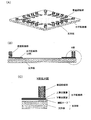
- FIG. 1 It is a figure which shows the electronic component for wiring comprised based on this invention
- (A) is a perspective view
- (B) is sectional drawing
- (C) has each shown the X section enlarged sectional view.
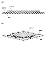
- FIG. 2A and 2B are diagrams showing a state in which a semiconductor LSI chip is bonded and connected as an electronic component on a substrate, where FIG. 2A shows a cross-sectional view and FIG. 2B shows a perspective view. It is a figure which shows the electronic component for wiring arrange
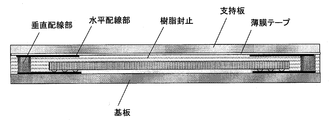
- FIG. 1A and 1B are diagrams showing an electronic component for wiring constructed according to the present invention, wherein FIG. 1A is a perspective view, FIG. 1B is a cross-sectional view, and FIG. 1C is an enlarged cross-sectional view of an X portion in FIG. Respectively.
- FIG. 1 illustrates a single unit pattern. In actual manufacturing, a single unit pattern is formed in a state of being connected to one another, and is manufactured by being incorporated in an electronic device package in that state, and then cut into individual chips. After being cut into individual pieces, it is completed as a final product.
- a thin film tape with a lower layer metal layer (for example, copper foil) is pasted on a support plate using an adhesive (hereinafter, a two-layer configuration of a thin film tape and a support plate). Called support part).
- a thin film tape and a thin metal film for example, copper foil
- a polyimide material can be apply
- a low-resistance metal film to be the lower metal layer is attached to the entire surface of the thin film tape by, for example, vapor deposition.
- this metal film in addition to copper Cu, for example, a conductive metal containing nickel Ni and chromium Cr can be used.
- the support plate any of a plate-like silicon substrate, an insulator such as glass, or a conductor can be used. For example, by using a stainless plate, stronger rigidity is obtained during the manufacture of a semiconductor device. be able to.
- an insulating base material of a thin film represented by a polyimide tape or the like, or an insulating base material such as a plastic resin used for an organic substrate is desirable.
- the support portion has a two-layer configuration of the insulating base tape and the support plate (reinforcement plate) attached to the back side (opposite side of the wiring pattern forming surface) using the adhesive. This support plate is peeled off and removed after the resin sealing step for manufacturing the electronic device package.
- the thin film tape is not limited to the single-layer thin film as illustrated, but is composed of a two-layer (or more) thin film tape bonded with an adhesive, and is attached to the support plate. It is also possible.
- the thin film tape functions as a protective film that covers the horizontal wiring (rewiring) in the finished product (electronic device package).
- the adhesive for attaching the thin film tape a material that is easily peeled off at a predetermined temperature (for example, high heat) or a material that is easily peeled off by ultraviolet irradiation is used.
- a heat-capsuled adhesive or a thermoplastic adhesive, or a support plate made of a material that transmits light (such as heat-resistant low-thermal expansion glass) and an ultraviolet peeling adhesive are used.
- an upper metal layer (for example, nickel) to be an etching mask for the lower metal layer is pasted on the lower metal layer.
- This attachment is performed by plating or vapor-depositing an upper metal layer (for example, nickel) on the lower metal layer.
- the upper metal layer is patterned by lithography. For this reason, a resist is applied on the upper metal layer, the pattern is exposed and developed, and further etched, and the resist is removed to complete the wiring pattern.
- the etching solution it is possible to etch only the upper metal layer without etching the lower metal layer.
- the lower metal layer is not etched until the plating filling is completed for the purpose of using it as a current-carrying metal electrode for electrolytic plating in the next plating filling step.
- a resist for forming a vertical wiring portion is applied to the entire surface including patterning of the formed upper metal layer, and an opening is formed by development.
- the resist opening is plated and filled.
- electrolytic plating is performed using the lower metal layer as a current-carrying metal electrode.
- FIG. 8 is a cross-sectional view showing the completed wiring electronic component.
- FIG. 8 corresponds to FIG. 1 described above.
- the lower metal layer is etched using the upper metal layer pattern exposed by removing the resist as an etching mask.
- the upper metal layer serving as a mask has already been patterned, so that no resist is required, and the patterning can be performed only by etching.
- a patterned horizontal wiring portion (upper metal layer and lower metal layer) is formed on the thin film tape.
- the horizontal wiring portion into a two-layer structure, the wiring having the horizontal wiring portion together with the vertical wiring portion using normal lithography and plating technology without using the electroforming method as in Patent Document 2.
- Electronic parts can be manufactured.
- the lower metal layer and the upper metal layer need to have conductivity, the lower metal layer can be used as a current-carrying metal electrode for vertical wiring portion plating, and the upper metal layer is an etching of the lower metal layer.
- the combination of the lower layer metal layer and the upper layer metal layer is not limited to the combination of copper and nickel exemplified, for example, Cu and Au, Ag, Cr and Cu, Cr and Ni, etc. As long as the combination of materials is high.
- a metal for vertical wiring parts what is necessary is just electroplating, and electroconductive metals, such as copper and nickel, can be used. Further, it is not always necessary to form the lower metal layer and the upper metal layer with a single metal layer, and it is possible to form a metal having good conductivity such as Au or Ag on any surface.
- FIGS. 9A and 9B are diagrams showing a state in which a semiconductor chip (LSI chip) is bonded and connected as an electronic component on a substrate, where FIG. 9A is a cross-sectional view and FIG. 9B is a perspective view.
- the illustrated substrate is exemplified as a silicon substrate (semiconductor substrate) having a wiring layer formed on the upper surface.
- a metal seed layer to be a wiring pattern is formed on the entire surface of the semiconductor substrate (for example, a sputtered layer or a nano metal material is coated).
- the seed layer for example, gold, silver, copper, or palladium foil that enables copper plating can be used.
- the wiring layer pattern is completed by applying a resist on the seed layer, exposing and developing the pattern, further etching, removing the resist.
- a wiring layer is grown on the seed layer by plating.
- the lithography process can be omitted by patterning the seed layer directly with nano metal particles. This direct patterning is a method in which nano metal particles such as copper are contained in an organic solvent and a desired pattern is drawn by an ink jet method which is practically used in a printer.
- the semiconductor LSI chip is illustrated as being flip-chip bonded to the wiring layer on the substrate.
- a bonding metal pad portion it is also possible to form a bonding metal pad portion to be a bonding wire connection electrode on the wiring layer on the substrate and connect it by a bonding wire.
- the metal pad portion on the wiring layer and the semiconductor LSI chip are connected by, for example, an Au bonding wire.
- FIG. 10 is a diagram showing the wiring electronic component (see FIG. 1 or FIG. 8) arranged on a substrate (see FIG. 9) on which a semiconductor LSI chip is mounted.
- FIG. 11 is a diagram showing a state in which electronic components for wiring are connected to a semiconductor substrate on which a semiconductor LSI chip is mounted.
- the substrate side is referred to as the back surface
- the wiring electronic component side disposed thereon is referred to as the front surface.
- a vertical wiring portion of the wiring electronic component is fixed and electrically connected to a predetermined position of the wiring layer formed on the upper surface of the substrate.
- connection electrode provided on the semiconductor substrate side
- the metal pad portion for the wiring is provided with a concave portion
- the wiring electronic component side can be formed by a method of providing a convex portion and inserting and crimping or caulking by inserting.
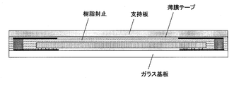
- FIG. 12 is a diagram showing the resin-sealed state. After the integrally connected vertical wiring portion is fixed at a predetermined position of the wiring layer, in this state, the upper surface of the substrate is transfer-molded to the thin film tape of the support portion and the lower surface of the horizontal wiring portion, or a liquid resin ( The material is resin-sealed using, for example, an epoxy system.
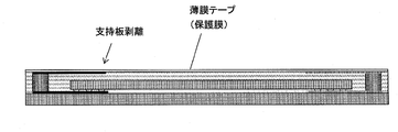
- FIG. 13 is a view showing the state after the support plate is peeled off.
- the support plate is peeled off by applying a predetermined temperature.
- the thin film tape exposed on the upper side of FIG. 13 functions as a protective film of the finished product.
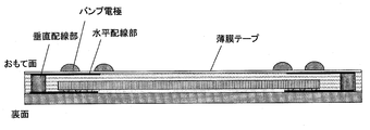
- FIG. 14 is a cross-sectional view showing the completed electronic device package. As shown in FIG. 14, on the front surface side, a hole is made in the thin film tape to form an external connection electrode (bump electrode) connected to the horizontal wiring portion exposed through the opening. With this horizontal wiring portion, an external connection electrode can be provided at a position different from the tip of the vertical wiring portion.
- an external connection electrode can be provided at a position different from the tip of the vertical wiring portion.
- a multilayer organic substrate as disclosed in Patent Document 2 or a lead frame can be used as such a substrate.
- an external connection electrode connected to the wiring layer on the upper surface of the substrate via the conductor layer inside the through hole can be easily formed on the back surface side of the substrate.
- the multilayer organic substrate is a substrate in which a wiring pattern is formed on each layer of a substrate composed of a plurality of layers, and then these substrates are bonded together, and through holes for connecting the wiring patterns of each layer are formed as necessary.
- a conductor layer is formed inside the through hole, and the conductor layer is connected to a land which is an end face electrode portion formed on the back surface side.
- the horizontal wiring part easily protected by the protective film on the front surface side, and the external connection electrode connected to the horizontal wiring part Can be formed.
- FIG. 15 is a diagram illustrating a state in which an electronic component such as an image sensor is mounted and connected on a glass substrate having a wiring layer (or a transparent resin substrate having good light transmittance).
- the image sensor is arranged with the light receiving surface facing downward.
- the wiring layer on the transparent glass substrate can be formed by the same method as the wiring layer on the semiconductor substrate described above with reference to FIG.
- An electronic component such as an image sensor (semiconductor LSI chip) is fixed and electrically connected using a wiring layer formed on a glass substrate as a bonding pad region.
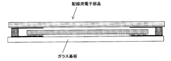
- FIG. 16 is a diagram showing a state in which electronic components for wiring are arranged on a glass substrate.
- FIG. 17 is a diagram showing a state in which the wiring electronic components are connected and fixed on the glass substrate. This connection is performed as described above with reference to FIG.
- FIG. 18 is a diagram showing the resin-sealed state after fixing.
- transfer molding is performed so as to fill the space between the glass substrate and the thin film tape, or resin sealing is performed using a liquid resin (the material is, for example, an epoxy system).
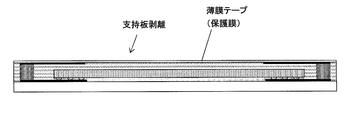
- FIG. 19 is a view showing the state after the support plate is peeled off. By peeling the support plate, the thin film tape exposed on the upper side functions as a protective film for the finished product.
- FIG. 20 is a view showing a completed image sensor chip package.
- a hole is made in the thin film tape, and a bump electrode for external connection connected to the wiring exposed through the opening is formed. Thereafter, the product is completed after being cut into individual chips and separated into pieces.
- FIG. 15 can be embodied in a high heat dissipation type chip package by using a high heat dissipation substrate that functions as a heat sink instead of the glass substrate described above.
- Example 3 is different from Example 2 only in that a high heat dissipation substrate that functions as a heat sink, a heat spreader, or the like is used (not shown).
- a high heat dissipation type LSI chip is mounted on a high heat dissipation substrate that functions as a heat sink, and there is no need for through electrodes, and an external connection electrode is formed on the front surface opposite to the high heat dissipation substrate.
- a heat dissipation chip package is completed.
Landscapes
- Internal Circuitry In Semiconductor Integrated Circuit Devices (AREA)
- Encapsulation Of And Coatings For Semiconductor Or Solid State Devices (AREA)
Abstract
本発明は、半導体チップを含む回路素子を配置して、該回路素子と外部電極に接続される水平配線部及び垂直配線部が内在する電子デバイスパッケージに組み込んで用いられる。支持板と該支持板に薄膜テープを貼り付けることにより支持部を構成する。下層金属層と該下層金属層をパターニングするためのマスクとして機能する上層金属層からなる2層構成の水平配線部を薄膜テープ上に形成する。電解メッキをすることにより、上層金属層に接続された垂直配線部を形成する。
Description
本発明は、半導体チップを含む回路素子を配置し、該回路素子から垂直配線を介して接続される外部電極を有する電子デバイスパッケージに組み込んで用いるための配線用電子部品及びその製造方法に関する。
外部接続用電極をおもて面に配置した電子デバイスパッケージ構造のように、LSIチップ搭載基板から離れて他方に電極を取り出す場合や、或いはウエハレベルチップサイズパッケージのようにLSIチップの能動面から離れて他方に電極を取り出す場合は、基板と離れて電極を取り出すための少なくとも垂直配線、あるいは再配線のための水平配線も含めた構造が必要である。一般的に電子デバイスパッケージ構造の垂直配線は基板に予め作りこんだ構造や樹脂封止後に樹脂を開口してメッキで埋める方法、さらにはシリコン基板を貫通させ、基板の両側に電極を取り出す構造が採られている(特許文献1参照)。
現在の貫通電極形成は低抵抗金属を充填するためには低温処理が要求され、半導体プロセスへの適用は難しく、一方、貫通孔の絶縁方法は、高温処理が必要なため半導体の実装プロセスへの適用は困難である。このように、半導体基板への貫通電極の形成とその絶縁方法にはまだ課題が残されていて、貫通電極を必要とせずに配線することが望まれる。
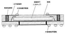
このような問題を解決するために、特許文献2は、部品化した配線用電子部品を半導体基板上の所定位置に接続することにより、貫通電極を必要とせずに配線する技術を開示する。図21及び図22は、特許文献2に開示の電子デバイスパッケージを説明する図であり、図21は、その製造途中の断面図であり、図22は、完成した状態で示す断面図である。図21に示すように、導電性材料の支持板に電鋳法により水平配線部(再配線)及び垂直配線部を成長させて、支持板と一体に連結した配線用電子部品を形成する。そして、この配線用電子部品を、半導体基板(多層有機基板)おもて面に形成した配線層上の所定位置に接続する。この後、図22に示すように、回路素子(LSIチップ)を覆う樹脂を充填して樹脂封止した後、支持板を剥がすことにより電気的には個々の水平配線部及び垂直配線部に分離して構成する。この水平配線部により、垂直配線部先端とは異なる位置に外部接続用電極を設けることができる。これによって、簡潔に、しかもコスト的にも安く外部接続用電極をおもて面に配置した電子デバイスパッケージを製造することが可能となる。
このように、電子デバイスパッケージ構造形成のための垂直配線や水平配線などの追加工程を部品として集約させ、工程を簡素化し部品は専門メーカに任せることでコスト低減を実現することができる。この部品化によりウエハレベルチップサイズパッケージなどは前工程に近い設備が必要な工程をオフラインで部品に集約することができ、これによって、後工程メーカも大きな投資の必要なく参入できることになる。
しかし、このような電子デバイスパッケージは、おもて面の水平配線部を保護するための保護膜を設ける場合、別途の工程として作成することが必要になる。また、例示の配線用電子部品を製造するための電鋳法は非常に優れた方法ではあるものの、電鋳法自体にはノウハウが多く、現状では製造業者が限られているという問題がある。
特開2001-127243号公報
国際公開WO 2008/065896 A1
本発明は、係る問題点を解決して、電子デバイスパッケージ構造形成のための垂直配線や水平配線などの追加工程を部品として集約させて、電子デバイスパッケージのおもて面に形成した配線パターンを保護するための保護膜を、簡潔に、しかもコスト的にも安く製造し、供給することを目的としている。
また、本発明は、電子デバイスパッケージに用いる配線用電子部品を、電鋳法を用いることなく従来より用いられている電解メッキとかリソグラフィなどの通常の製造技術を用いて容易に作成可能にすることを目的としている。
本発明の配線用電子部品は、半導体チップを含む回路素子を配置して、該回路素子と外部電極に接続される水平配線部及び垂直配線部が内在する電子デバイスパッケージに組み込んで用いられる。支持板と該支持板に電子デバイスパッケージの保護膜として機能する薄膜テープを貼り付けることにより2層構成の支持部を構成する。下層金属層と該下層金属層をパターニングするためのマスクとして機能する上層金属層からなる2層構成の水平配線部を薄膜テープ上に形成する。下層金属層を通電用金属電極として用いて電解メッキをすることにより、上層金属層に接続された垂直配線部を形成する。
また、本発明の電子デバイスパッケージに組み込んで用いるための配線用電子部品の製造方法は、支持板の上に、下層金属層付きの薄膜テープを接着剤を用いて貼り付け、下層金属層の上に、該下層金属層のためのエッチングマスクとなるべき上層金属層を貼り付け、該上層金属層のパターニングをリソグラフィにより行って、配線パターンを形成する。垂直配線部形成用のレジストを塗布し、現像で開口した後、下層金属層を通電用金属電極として用いて電解メッキをすることにより、レジスト開口部にメッキ充填し、かつ、このレジストを除去することによって、上層金属層パターンに接続された垂直配線部を形成する。この上層金属層パターンをエッチング用マスクとして、下層金属層をエッチングすることによって、薄膜テープの上にパターニングした2層構成の水平配線部を形成する。
また、本発明の電子デバイスパッケージ及びその製造方法は、配線用電子部品を、支持板と該支持板に薄膜テープを貼り付けることにより構成した2層構成の支持部と、該支持部上に形成される水平配線部と、該水平配線部に接続される垂直配線部により構成する。水平配線部は、下層金属層と該下層金属層をパターニングするためのマスクとして機能する上層金属層からなる2層構成にして薄膜テープ上に形成する。垂直配線部は、下層金属層を通電用金属電極として用いて電解メッキをすることにより形成する。配線用電子部品の垂直配線部を、基板上の配線層の所定位置に接続しかつ固定して樹脂封止した後、支持板を剥離することにより露出した薄膜テープを保護膜として用い、かつ、この保護膜に穴を空け、開口により露出した水平配線部と接続される外部電極を形成する。
本発明によれば、電子デバイスパッケージ形成のための垂直配線や水平配線などの追加工程を部品として集約させて、電子デバイスパッケージのおもて面に形成した水平配線部(再配線)を保護するための保護膜を、簡潔に、しかもコスト的にも安く製造し、供給することができる。
また、本発明は、電子デバイスパッケージに用いる配線用電子部品を、電鋳法を用いることなく従来より用いられている通常の製造技術を用いて容易に作成することができる。
また、本発明によれば、簡易な方法で、イメージセンサあるいは高放熱のパッケージのような基板と反対側に電極を取り出す必要のある半導体パッケージを製作できる。半導体基板に貫通孔を開けて金属材料を充填する貫通配線技術の必要も無く、半導体基板と反対側に容易に電極を取り出し、かつ配線することができる。
以下、例示に基づき、本発明の配線用電子部品及びその製造方法を、順を追って説明する。図1は、本発明に基づき構成した配線用電子部品を示す図であり、(A)は斜視図、(B)は断面図、(C)は(B)中のX部を拡大した断面図をそれぞれ示している。図1は、1個の単体パターンを例示するが、実際の製造においては、多数個一体に連結された状態で作成され、その状態で電子デバイスパッケージに組み込んで製造した後、個々のチップに切断して切り分ける個片化を経て、最終製品として完成する。
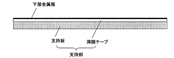
次に、このような配線用電子部品の製造について、図2~図8を参照して、順次説明する。まず、図2に示すように、支持板の上に、下層金属層(例えば、銅箔)付きの薄膜テープを、接着剤を用いて貼り付ける(以下、薄膜テープと支持板の2層構成を支持部と言う)。下層金属層付きの薄膜テープとしては、薄膜テープと薄い金属膜(例えば銅箔)を一体化したものを用いる。例えば、銅箔とポリイミドテープとの一体化を作る場合、銅箔の上にポリイミド材を塗って作製することができる。或いは、薄膜テープ上の全面に、下層金属層となるべき低抵抗の金属膜を、例えば蒸着により貼り付ける。この金属膜としては、銅Cu以外にも、例えば、ニッケルNi、クロムCrを含む導電性金属を用いることができる。
支持板としては、板状のシリコン基板とかガラスのような絶縁体或いは導電体のいずれも用いることができるが、例えば、ステンレス板を用いることにより、半導体装置の製造中に、より強い剛性を得ることができる。貼り付ける薄膜テープとしては、ポリイミドテープなどに代表される薄膜フィルムの絶縁基材とか、有機基板に用いられているようなプラスチック樹脂等の絶縁基材が望ましい。このように、支持部は、絶縁基材テープと、この裏側(配線パターン形成面の反対側)に接着剤を用いて貼り付けた支持板(補強板)との2層構成となる。この支持板は、電子デバイスパッケージ製造のための樹脂封止工程後に、剥離して除去する。また、薄膜テープは、例示したような一層の薄膜フィルムに限らず、接着剤により接着した2層(或いはそれ以上)の薄膜フィルムの絶縁基材テープにより構成にして、支持板の上に貼り付けることも可能である。
薄膜テープは、完成製品(電子デバイスパッケージ)において水平配線部(再配線)を覆う保護膜として機能する。薄膜テープを貼り付ける接着剤は、所定の温度(例えば、高熱)で剥離し易い材料か、紫外線照射で剥離し易い材料を用いる。例えば、熱カプセル入り接着剤又は熱可塑性の接着剤、若しくは、光を透過する材料(耐熱低熱膨張ガラスなど)の支持板と、紫外線剥離型接着剤を用いる。
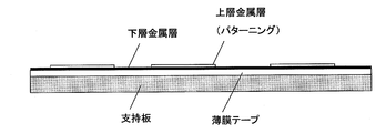
次に、図3に示すように、下層金属層の上に、下層金属層のためのエッチングマスクとなるべき上層金属層(例えば、ニッケル)を貼り付ける。この貼り付けは、下層金属層の上に上層金属層(例えば、ニッケル)をメッキ又は蒸着することにより行う。
次に、図4に示すように、この上層金属層のパターニングをリソグラフィにより実施する。このため、上層金属層の上にレジストを塗布し、パターンを露光、現像してさらにエッチングを行い、レジストを除去して、配線パターンを完成させる。エッチング液を選択することにより、下層金属層をエッチングすることなく、上層金属層のみをエッチングすることが可能である。この際、下層金属層は、次のメッキ充填工程で、電解メッキのための通電用金属電極として用いる目的のために、メッキ充填が終わるまで、エッチングしない。
次に、図5に示すように、形成した上層金属層のパターニングを含む全面に、垂直配線部形成用のレジストを塗布し、現像で開口する。
次に、図6に示すように、レジスト開口部にメッキを施して充填する。このメッキ充填のために、下層金属層を通電用金属電極として用いて電解メッキをする。電解メッキを用いたメッキ充填を可能にすることにより、無電解メッキに比較して速度が早く、コストダウンを図ることが可能となる。
次に、図7に示すように、レジストを除去することによって、上層金属層パターンに接続された垂直配線部が形成される。
図8は、完成した配線用電子部品を示す断面図である。図8は、上述した図1に相当する。レジストを除去することにより露出した上層金属層パターンを、エッチング用マスクとして、下層金属層をエッチングする。下層金属層のエッチングに際して、そのマスクとなる上層金属層は既にパターニングされているので、レジストは不要で、いきなりエッチングだけでパターニングが可能となる。これによって、薄膜テープの上にパターニングした2層構成の水平配線部(上層金属層と下層金属層)が形成される。
このように、水平配線部を2層構成とすることにより、特許文献2のような電鋳法を用いること無く、通常のリソグラフィ及びメッキ技術を用いて、垂直配線部と共に水平配線部を有する配線用電子部品の製造が可能となる。なお、下層金属層及び上層金属層は導電性を有する必要があることに加えて、下層金属層は垂直配線部メッキ用の通電用金属電極として使用できること、及び上層金属層は下層金属層のエッチング用マスクとして使用できるものであれば、下層金属層と上層金属層の組み合わせは、例示した銅とニッケルの組み合わせ以外にも、例えばCuとAu,AgやCrとCu、CrとNi等選択エッチング製の高い材料の組合せであれば良い。また、垂直配線部用金属としては、電解メッキ可能であれば良く、銅、ニッケルなどの導電性金属を使用可能である。また、下層金属層と上層金属層は、いずれも単一金属層により形成する必要は必ずしも無く、いずれかの表面にAuやAg等といった導電性の良い金属を形成することも可能である。
次に、上述の配線電子部品を用いて構成される電子デバイスパッケージの製造について説明する。図9は、基板上に、電子部品として半導体チップ(LSIチップ)を接着し、かつ接続した状態で示す図であり、(A)は断面図を、(B)は斜視図を示している。例示の基板は、上面に配線層を形成したシリコン基板(半導体基板)として例示している。
半導体基板上に配線層を形成するために、半導体基板の全面に、配線パターンとなるべき金属のシード層を形成する(例えばスパッタ層あるいはナノ金属材料を塗膜)。このシード層としては、例えば、銅メッキを可能とする金、銀、銅、パラジューム箔を用いることができる。配線層のパターンはシード層の上にレジストを塗布し、パターンを露光、現像してさらにエッチングを行い、レジストを除去して完成させる。このシード層の上にメッキにより配線層を成長させる。或いは、ナノ金属粒子で直接シード層をパターニングにしてリソグラフィ工程を省略することもできる。この直接パターニングは、有機溶媒中に銅等のナノ金属粒子を含有させて、それをプリンターで実用されているインクジェット法で所望のパターンを描く方法である。
半導体LSIチップは、基板上の配線層とはフリップチップボンド接続するものとして例示している。このフリップチップボンド接続に代えて、基板上の配線層に、ボンディングワイヤ接続電極となるボンディング用金属パッド部を形成して、ボンディングワイヤにより接続することも可能である。この場合、配線層上の金属パッド部と半導体LSIチップは、例えば、Auボンディングワイヤにより接続される。
図10は、上述の配線用電子部品(図1又は図8参照)を、半導体LSIチップを装着した基板(図9参照)上に配置した状態で示す図である。
図11は、配線用電子部品を、半導体LSIチップを装着した半導体基板上に接続した状態で示す図である。なお、図示したように、基板側を裏面として、その上に配置される配線用電子部品側をおもて面と称する。基板上面に形成した配線層の所定の位置には、配線用電子部品の垂直配線部が固定され、かつ電気的に接続される。垂直配線部を固定及び接続する手法としては、(1)超音波による接合、(2)銀ペースト等の導電性ペーストによる接続、(3)半田接続、(4)半導体基板側に設けた接続電極用金属パッド部に凹部を設ける一方、配線用電子部品側は凸部を設けて挿入圧着あるいは挿入してカシメる方法、により行うことができる。
図12は、樹脂封止した状態で示す図である。一体に連結されている垂直配線部が配線層の所定の位置に固定された後、この状態で、基板の上面は、支持部の薄膜テープ及び水平配線部下面までトランスファーモールドされ、或いは液状樹脂(材質は、例えばエポキシ系)を用いて樹脂封止される。
図13は、支持板を剥離した後の状態で示す図である。例えば、所定の温度を加えることにより、支持板を剥離する。これにより図13の上側に露出した薄膜テープは、完成製品の保護膜として機能する。
図14は、完成した電子デバイスパッケージを示す断面図である。図14に示すように、おもて面側においては、薄膜テープに穴を空け、開口により露出した水平配線部と接続される外部接続用電極(バンプ電極)を形成する。この水平配線部により、垂直配線部先端とは異なる位置に外部接続用電極を設けることができる。
以上、基板として半導体シリコン基板を用いる場合を例として説明したが、このような基板としては、特許文献2に開示のような多層有機基板とか或いはリードフレームを用いることも可能である。多層有機基板を用いた際には、スルーホール内部の導体層を介して基板上面の配線層に接続される外部接続用電極を、基板裏面側においても容易に形成することができる。多層有機基板は、複数層から成る基板の各層に、それぞれ配線パターンを形成した後これらの基板を貼り合わせ、必要に応じて各層の配線パターンを接続するためのスルーホールを形成したものである。このスルーホールの内部には導体層が形成され、この導体層が裏面側に形成された端面電極部であるランドと接続されている。
このように、本発明は、例示の配線用電子部品を用いることにより、おもて面側に容易に保護膜により保護された水平配線部、及びこの水平配線部に接続された外部接続用電極を形成することが可能になる。
次に、本発明の配線用電子部品をイメージセンサチップパッケージに用いた例を、図15~図20を参照して説明する。図15は、配線層を有するガラス基板(又は光透過性の良い透明樹脂基板)の上に、イメージセンサのような電子部品が搭載されて接続された状態で示す図である。イメージセンサは、受光面を下側に向けて配置する。透明ガラス基板上の配線層は、図9を参照して上述した半導体基板上の配線層と同様な方法で形成することができる。ガラス基板に形成した配線層をボンディングパッド領域として、イメージセンサ(半導体LSIチップ)のような電子部品を固定しかつ電気的に接続する。
図16は、ガラス基板上に配線用電子部品を配置した状態で示す図である。図17は、ガラス基板上に配線用電子部品を接続、固定した状態で示す図である。この接続は、図11を参照して前述したように行う。
図18は、固定後、樹脂封止した状態で示す図である。図12を参照して前述したようにして、ガラス基板と薄膜テープの間の空間を満たすようにトランスファーモールドされ、或いは液状樹脂(材質は、例えばエポキシ系)を用いて樹脂封止される。
図19は、支持板を剥離した後の状態で示す図である。支持板を剥離することにより、上側に露出した薄膜テープは、完成製品の保護膜として機能する。
次に、図20に示すように、天地(上下)逆転させる。図20は、完成したイメージセンサチップパッケージを示す図である。図20の下側に位置するおもて面側においては、薄膜テープに穴を空け、開口により露出した配線と接続される外部接続用のバンプ電極を形成する。この後、個々のチップに切断して切り分ける個片化を経た後に、製品として完成させる。
図15において上述したガラス基板に代えて、ヒートシンクとして機能する高放熱基板を用いることにより、高放熱型チップパッケージに具体化することができる。実施例3は、ヒートシンク、ヒートスプレッダー等として機能する高放熱基板を用いた点でのみ実施例2とは相違する(図示省略)。
これによって、ヒートシンクとして機能する高放熱基板に、高放熱型のLSIチップが実装されて、貫通電極の必要なく、高放熱基板とは反対側のおもて面に外部接続用電極を形成した高放熱型チップパッケージが完成する。
以上、本開示にて幾つかの実施の形態のみを単に一例として詳細に説明したが、本発明の新規な教示及び有利な効果から実質的に逸脱せずに、その実施の形態には多くの改変例が可能である。
Claims (15)
- 半導体チップを含む回路素子を配置して、該回路素子と外部電極に接続される水平配線部及び垂直配線部が内在する電子デバイスパッケージに組み込んで用いるための配線用電子部品において、
支持板と該支持板に電子デバイスパッケージの保護膜として機能する薄膜テープを貼り付けることにより支持部を構成し、
下層金属層と該下層金属層をパターニングするためのマスクとして機能する上層金属層からなる構成の前記水平配線部を前記薄膜テープ上に形成し、
前記下層金属層を通電用金属電極として用いて電解メッキをすることにより、前記上層金属層に接続された前記垂直配線部を形成したことから成る配線用電子部品。 - 前記支持板として、板状のシリコン基板、ガラスのような絶縁体或いは導電体のいずれかを用いる請求項1に記載の配線用電子部品。
- 前記薄膜テープとして、一層の薄膜フィルム或いは接着剤により接着した2層以上の薄膜フィルムの絶縁基材を用いる請求項1に記載の配線用電子部品。
- 半導体チップを含む回路素子を配置して、該回路素子と外部電極に接続される水平配線部及び垂直配線部が内在する電子デバイスパッケージに組み込んで用いるための配線用電子部品の製造方法において、
支持板の上に、下層金属層付きの薄膜テープを接着剤を用いて貼り付け、
前記下層金属層の上に、該下層金属層のためのエッチングマスクとなるべき上層金属層を貼り付け、
該上層金属層のパターニングをリソグラフィにより行って、配線パターンを形成し、
垂直配線部形成用のレジストを塗布し、現像で開口した後、前記下層金属層を通電用金属電極として用いて電解メッキをすることにより、レジスト開口部にメッキ充填し、かつ、このレジストを除去することによって、前記上層金属層パターンに接続された前記垂直配線部を形成し、
前記上層金属層パターンをエッチング用マスクとして、前記下層金属層をエッチングすることによって、前記薄膜テープの上にパターニングした構成の前記水平配線部を形成したことからなる配線用電子部品の製造方法。 - 前記支持板として、板状のシリコン基板、ガラスのような絶縁体或いは導電体のいずれかを用いる請求項4に記載の配線用電子部品の製造方法。
- 前記薄膜テープとして、一層の薄膜フィルム或いは接着剤により接着した2層以上の薄膜フィルムの絶縁基材を用いる請求項4に記載の配線用電子部品の製造方法。
- 前記下層金属層付きの薄膜テープとして、薄膜テープと薄い金属膜を一体化して形成し、或いは、薄膜テープ上の全面に下層金属層となるべき低抵抗の金属膜を蒸着あるいは貼り付けることにより形成した請求項4に記載の配線用電子部品の製造方法。
- 前記薄膜テープは、前記電子デバイスパッケージにおいて水平配線部を覆う保護膜として機能する請求項4に記載の配線用電子部品の製造方法。
- 前記薄膜テープを貼り付ける接着剤は、所定の温度で剥離し易い材料か、紫外線照射で剥離し易い材料を用いる請求項4に記載の配線用電子部品の製造方法。
- 前記上層金属層は、前記下層金属層の上にメッキ又は蒸着することによって貼り付けられる請求項4に記載の配線用電子部品の製造方法。
- 前記上層金属層のパターニングは、該上層金属層の上にレジストを塗布し、パターンを露光、現像してさらにエッチングを行い、レジストを除去して、配線パターンを完成させる請求項4に記載の配線用電子部品の製造方法。
- 半導体チップを含む回路素子を配置して、該回路素子と外部電極に接続される水平配線部及び垂直配線部が内在する電子デバイスパッケージにおいて、
配線用電子部品を、支持板と該支持板に薄膜テープを貼り付けることにより構成した支持部と、該支持部上に形成される前記水平配線部と、該水平配線部に接続される前記垂直配線部により構成し、
前記水平配線部は、下層金属層と該下層金属層をパターニングするためのマスクとして機能する上層金属層からなる構成にして前記薄膜テープ上に形成し、
前記垂直配線部は、前記下層金属層を通電用金属電極として用いて電解メッキをすることにより形成し、
前記配線用電子部品の前記垂直配線部を、基板上の配線層の所定位置に接続しかつ固定して樹脂封止した後、前記支持板を剥離することにより露出した薄膜テープを保護膜として用い、かつ、この保護膜に穴を空け、開口により露出した前記水平配線部と接続される前記外部電極を形成したことから成る電子デバイスパッケージ。 - 配線層を有する前記基板がガラス基板又は光透過性の良い透明樹脂基板であり、該基板上に配置される回路素子がイメージセンサである請求項12に記載の電子デバイスパッケージ。
- 配線層を有する前記基板がヒートシンク或いはヒートスプレッダーとして機能する高放熱基板であり、該基板上に配置される回路素子が高放熱型のLSIチップである請求項12に記載の電子デバイスパッケージ。
- 半導体チップを含む回路素子を配置して、該回路素子と外部電極に接続される水平配線部及び垂直配線部が内在する電子デバイスパッケージの製造方法において、
配線用電子部品を、支持板と該支持板に薄膜テープを貼り付けることにより構成した支持部と、該支持部上に形成される前記水平配線部と、該水平配線部に接続される前記垂直配線部により構成し、
前記水平配線部は、下層金属層と該下層金属層をパターニングするためのマスクとして機能する上層金属層からなる構成にして前記薄膜テープ上に形成し、
前記垂直配線部は、前記下層金属層を通電用金属電極として用いて電解メッキをすることにより形成し、
前記配線用電子部品の前記垂直配線部を、基板上の配線層の所定位置に接続しかつ固定して樹脂封止した後、前記支持板を剥離することにより露出した薄膜テープを保護膜として用い、かつ、この保護膜に穴を空け、開口により露出した前記水平配線部と接続される前記外部電極を形成したことから成る電子デバイスパッケージの製造方法。
Applications Claiming Priority (2)
| Application Number | Priority Date | Filing Date | Title |
|---|---|---|---|
| JP2008297474A JP2010123821A (ja) | 2008-11-21 | 2008-11-21 | 配線用電子部品及びその製造方法、並びに該配線用電子部品を組み込んで用いる電子デバイスパッケージ及びその製造方法 |
| JP2008-297474 | 2008-11-21 |
Publications (1)
| Publication Number | Publication Date |
|---|---|
| WO2010058595A1 true WO2010058595A1 (ja) | 2010-05-27 |
Family
ID=42198038
Family Applications (1)
| Application Number | Title | Priority Date | Filing Date |
|---|---|---|---|
| PCT/JP2009/006267 Ceased WO2010058595A1 (ja) | 2008-11-21 | 2009-11-20 | 配線用電子部品及びその製造方法、並びに該配線用電子部品を組み込んで用いる電子デバイスパッケージ及びその製造方法 |
Country Status (3)
| Country | Link |
|---|---|
| JP (1) | JP2010123821A (ja) |
| TW (1) | TW201029122A (ja) |
| WO (1) | WO2010058595A1 (ja) |
Families Citing this family (1)
| Publication number | Priority date | Publication date | Assignee | Title |
|---|---|---|---|---|
| JP6495692B2 (ja) | 2015-03-11 | 2019-04-03 | 東芝メモリ株式会社 | 半導体装置及びその製造方法 |
Citations (3)
| Publication number | Priority date | Publication date | Assignee | Title |
|---|---|---|---|---|
| JPH1145955A (ja) * | 1997-07-28 | 1999-02-16 | Kyocera Corp | 素子内蔵多層配線基板およびその製造方法 |
| JP2007158193A (ja) * | 2005-12-07 | 2007-06-21 | Matsushita Electric Ind Co Ltd | 電子部品実装用基板、電子部品モジュール、電子部品実装構造体及びこれらの製造方法 |
| JP2008235378A (ja) * | 2007-03-16 | 2008-10-02 | Nec Corp | 金属ポストを有する配線基板、半導体装置及び製造方法 |
Family Cites Families (1)
| Publication number | Priority date | Publication date | Assignee | Title |
|---|---|---|---|---|
| US5017271A (en) * | 1990-08-24 | 1991-05-21 | Gould Inc. | Method for printed circuit board pattern making using selectively etchable metal layers |
-
2008
- 2008-11-21 JP JP2008297474A patent/JP2010123821A/ja active Pending
-
2009
- 2009-11-20 WO PCT/JP2009/006267 patent/WO2010058595A1/ja not_active Ceased
- 2009-11-20 TW TW098139621A patent/TW201029122A/zh unknown
Patent Citations (3)
| Publication number | Priority date | Publication date | Assignee | Title |
|---|---|---|---|---|
| JPH1145955A (ja) * | 1997-07-28 | 1999-02-16 | Kyocera Corp | 素子内蔵多層配線基板およびその製造方法 |
| JP2007158193A (ja) * | 2005-12-07 | 2007-06-21 | Matsushita Electric Ind Co Ltd | 電子部品実装用基板、電子部品モジュール、電子部品実装構造体及びこれらの製造方法 |
| JP2008235378A (ja) * | 2007-03-16 | 2008-10-02 | Nec Corp | 金属ポストを有する配線基板、半導体装置及び製造方法 |
Also Published As
| Publication number | Publication date |
|---|---|
| JP2010123821A (ja) | 2010-06-03 |
| TW201029122A (en) | 2010-08-01 |
Similar Documents
| Publication | Publication Date | Title |
|---|---|---|
| KR101150322B1 (ko) | 반도체 칩 패키지 및 그 제조 방법 | |
| KR101193416B1 (ko) | 3차원 실장 반도체 장치 및 그의 제조 방법 | |
| JP4274290B2 (ja) | 両面電極構造の半導体装置の製造方法 | |
| TWI316749B (en) | Semiconductor package and fabrication method thereof | |
| JP2019512168A (ja) | シリコン基板に埋め込まれたファンアウト型の3dパッケージ構造 | |
| KR101195786B1 (ko) | 칩 사이즈 양면 접속 패키지의 제조 방법 | |
| JP2005506678A (ja) | 集積型ヒートシンク及びビルドアップ層を有する超小型電子パッケージ | |
| US20130127004A1 (en) | Image Sensor Module Package and Manufacturing Method Thereof | |
| WO2009123048A1 (ja) | 配線用電子部品及びその製造方法 | |
| JP2009070882A (ja) | 半導体チップパッケージ及びその製造方法 | |
| KR20070101094A (ko) | 전자 장치용 기판 및 그 제조 방법, 및 전자 장치 및 그제조 방법 | |
| JP5665020B2 (ja) | 配線用電子部品の製造方法 | |
| JP3732378B2 (ja) | 半導体装置の製造方法 | |
| JP2010245157A (ja) | 配線用部品及びその製造方法、並びに該配線用部品を組み込んで用いる電子デバイスパッケージ及びその製造方法 | |
| JP5429890B2 (ja) | 配線用電子部品及びその製造方法、並びに該配線用電子部品を組み込んで用いる電子デバイスパッケージ及びその製造方法 | |
| JPH0864635A (ja) | 半導体装置 | |
| WO2010058595A1 (ja) | 配線用電子部品及びその製造方法、並びに該配線用電子部品を組み込んで用いる電子デバイスパッケージ及びその製造方法 | |
| JP2009021267A (ja) | 外部接続用電極を配置した半導体装置及びその製造方法 | |
| JP5491722B2 (ja) | 半導体装置パッケージ構造及びその製造方法 | |
| KR20130027870A (ko) | 패키지 기판 및 패키지의 제조 방법 | |
| JP2010161101A (ja) | 配線用電子部品及びその製造方法、並びに該配線用電子部品を組み込んで用いる電子デバイスパッケージ及びその製造方法 | |
| JP5982414B2 (ja) | 半導体装置パッケージ構造及びその製造方法 | |
| JP2009059771A (ja) | ウエハレベルチップサイズパッケージ及びその製造方法 | |
| CN107170715A (zh) | 半导体封装结构及其制作方法 | |
| JP2014143448A (ja) | 配線用電子部品及びその製造方法 |
Legal Events
| Date | Code | Title | Description |
|---|---|---|---|
| 121 | Ep: the epo has been informed by wipo that ep was designated in this application |
Ref document number: 09827376 Country of ref document: EP Kind code of ref document: A1 |
|
| NENP | Non-entry into the national phase |
Ref country code: DE |
|
| 122 | Ep: pct application non-entry in european phase |
Ref document number: 09827376 Country of ref document: EP Kind code of ref document: A1 |