WO2010050021A1 - 化合物半導体装置及びその製造方法 - Google Patents
化合物半導体装置及びその製造方法 Download PDFInfo
- Publication number
- WO2010050021A1 WO2010050021A1 PCT/JP2008/069676 JP2008069676W WO2010050021A1 WO 2010050021 A1 WO2010050021 A1 WO 2010050021A1 JP 2008069676 W JP2008069676 W JP 2008069676W WO 2010050021 A1 WO2010050021 A1 WO 2010050021A1
- Authority
- WO
- WIPO (PCT)
- Prior art keywords
- layer
- compound semiconductor
- forming
- semiconductor device
- gan layer
- Prior art date
Links
- 150000001875 compounds Chemical class 0.000 title claims abstract description 70
- 239000004065 semiconductor Substances 0.000 title claims abstract description 69
- 238000004519 manufacturing process Methods 0.000 title claims description 28
- 238000000034 method Methods 0.000 title claims description 22
- 229910002704 AlGaN Inorganic materials 0.000 claims abstract description 25
- 239000000758 substrate Substances 0.000 claims description 32
- 239000010410 layer Substances 0.000 description 180
- 239000007789 gas Substances 0.000 description 28
- VYPSYNLAJGMNEJ-UHFFFAOYSA-N Silicium dioxide Chemical compound O=[Si]=O VYPSYNLAJGMNEJ-UHFFFAOYSA-N 0.000 description 21
- 229910052814 silicon oxide Inorganic materials 0.000 description 19
- 229910052581 Si3N4 Inorganic materials 0.000 description 11
- HQVNEWCFYHHQES-UHFFFAOYSA-N silicon nitride Chemical compound N12[Si]34N5[Si]62N3[Si]51N64 HQVNEWCFYHHQES-UHFFFAOYSA-N 0.000 description 11
- 238000002488 metal-organic chemical vapour deposition Methods 0.000 description 10
- JLTRXTDYQLMHGR-UHFFFAOYSA-N trimethylaluminium Chemical compound C[Al](C)C JLTRXTDYQLMHGR-UHFFFAOYSA-N 0.000 description 7
- QGZKDVFQNNGYKY-UHFFFAOYSA-N Ammonia Chemical compound N QGZKDVFQNNGYKY-UHFFFAOYSA-N 0.000 description 6
- 238000010586 diagram Methods 0.000 description 6
- IBEFSUTVZWZJEL-UHFFFAOYSA-N trimethylindium Chemical compound C[In](C)C IBEFSUTVZWZJEL-UHFFFAOYSA-N 0.000 description 6
- PMHQVHHXPFUNSP-UHFFFAOYSA-M copper(1+);methylsulfanylmethane;bromide Chemical compound Br[Cu].CSC PMHQVHHXPFUNSP-UHFFFAOYSA-M 0.000 description 5
- 239000013078 crystal Substances 0.000 description 5
- 238000009826 distribution Methods 0.000 description 5
- 238000005530 etching Methods 0.000 description 5
- 238000002955 isolation Methods 0.000 description 5
- XCZXGTMEAKBVPV-UHFFFAOYSA-N trimethylgallium Chemical compound C[Ga](C)C XCZXGTMEAKBVPV-UHFFFAOYSA-N 0.000 description 5
- VEXZGXHMUGYJMC-UHFFFAOYSA-N Hydrochloric acid Chemical compound Cl VEXZGXHMUGYJMC-UHFFFAOYSA-N 0.000 description 3
- XUIMIQQOPSSXEZ-UHFFFAOYSA-N Silicon Chemical compound [Si] XUIMIQQOPSSXEZ-UHFFFAOYSA-N 0.000 description 3
- 229910021529 ammonia Inorganic materials 0.000 description 3
- 230000000903 blocking effect Effects 0.000 description 3
- 238000001784 detoxification Methods 0.000 description 3
- 230000000694 effects Effects 0.000 description 3
- 239000012535 impurity Substances 0.000 description 3
- 229910052710 silicon Inorganic materials 0.000 description 3
- 239000010703 silicon Substances 0.000 description 3
- 230000005533 two-dimensional electron gas Effects 0.000 description 3
- 238000011144 upstream manufacturing Methods 0.000 description 3
- OKTJSMMVPCPJKN-UHFFFAOYSA-N Carbon Chemical compound [C] OKTJSMMVPCPJKN-UHFFFAOYSA-N 0.000 description 2
- VEXZGXHMUGYJMC-UHFFFAOYSA-M Chloride anion Chemical compound [Cl-] VEXZGXHMUGYJMC-UHFFFAOYSA-M 0.000 description 2
- 229910052799 carbon Inorganic materials 0.000 description 2
- 230000007423 decrease Effects 0.000 description 2
- 238000002474 experimental method Methods 0.000 description 2
- 229910000041 hydrogen chloride Inorganic materials 0.000 description 2
- IXCSERBJSXMMFS-UHFFFAOYSA-N hydrogen chloride Substances Cl.Cl IXCSERBJSXMMFS-UHFFFAOYSA-N 0.000 description 2
- 239000011241 protective layer Substances 0.000 description 2
- 239000010453 quartz Substances 0.000 description 2
- 229910052594 sapphire Inorganic materials 0.000 description 2
- 239000010980 sapphire Substances 0.000 description 2
- KZBUYRJDOAKODT-UHFFFAOYSA-N Chlorine Chemical compound ClCl KZBUYRJDOAKODT-UHFFFAOYSA-N 0.000 description 1
- 229910001218 Gallium arsenide Inorganic materials 0.000 description 1
- JMASRVWKEDWRBT-UHFFFAOYSA-N Gallium nitride Chemical compound [Ga]#N JMASRVWKEDWRBT-UHFFFAOYSA-N 0.000 description 1
- BLRPTPMANUNPDV-UHFFFAOYSA-N Silane Chemical compound [SiH4] BLRPTPMANUNPDV-UHFFFAOYSA-N 0.000 description 1
- 230000015556 catabolic process Effects 0.000 description 1
- 238000005229 chemical vapour deposition Methods 0.000 description 1
- XOYLJNJLGBYDTH-UHFFFAOYSA-M chlorogallium Chemical group [Ga]Cl XOYLJNJLGBYDTH-UHFFFAOYSA-M 0.000 description 1
- 230000007547 defect Effects 0.000 description 1
- 238000000151 deposition Methods 0.000 description 1
- 238000000407 epitaxy Methods 0.000 description 1
- 229910052736 halogen Inorganic materials 0.000 description 1
- 150000002367 halogens Chemical class 0.000 description 1
- 238000010438 heat treatment Methods 0.000 description 1
- 230000006698 induction Effects 0.000 description 1
- 239000011777 magnesium Substances 0.000 description 1
- QBJCZLXULXFYCK-UHFFFAOYSA-N magnesium;cyclopenta-1,3-diene Chemical compound [Mg+2].C1C=CC=[C-]1.C1C=CC=[C-]1 QBJCZLXULXFYCK-UHFFFAOYSA-N 0.000 description 1
- 239000000463 material Substances 0.000 description 1
- 229910052751 metal Inorganic materials 0.000 description 1
- 239000002184 metal Substances 0.000 description 1
- 150000004767 nitrides Chemical class 0.000 description 1
- 238000002161 passivation Methods 0.000 description 1
- 239000012071 phase Substances 0.000 description 1
- 238000005268 plasma chemical vapour deposition Methods 0.000 description 1
- 238000005498 polishing Methods 0.000 description 1
- 230000005855 radiation Effects 0.000 description 1
- 239000002994 raw material Substances 0.000 description 1
- 230000001846 repelling effect Effects 0.000 description 1
- 229910000077 silane Inorganic materials 0.000 description 1
- 125000006850 spacer group Chemical group 0.000 description 1
- 239000000126 substance Substances 0.000 description 1
- -1 thickness Substances 0.000 description 1
- 238000000927 vapour-phase epitaxy Methods 0.000 description 1
Images


Classifications
-
- H—ELECTRICITY
- H01—ELECTRIC ELEMENTS
- H01L—SEMICONDUCTOR DEVICES NOT COVERED BY CLASS H10
- H01L21/00—Processes or apparatus adapted for the manufacture or treatment of semiconductor or solid state devices or of parts thereof
- H01L21/02—Manufacture or treatment of semiconductor devices or of parts thereof
- H01L21/04—Manufacture or treatment of semiconductor devices or of parts thereof the devices having at least one potential-jump barrier or surface barrier, e.g. PN junction, depletion layer or carrier concentration layer
- H01L21/18—Manufacture or treatment of semiconductor devices or of parts thereof the devices having at least one potential-jump barrier or surface barrier, e.g. PN junction, depletion layer or carrier concentration layer the devices having semiconductor bodies comprising elements of Group IV of the Periodic System or AIIIBV compounds with or without impurities, e.g. doping materials
-
- H—ELECTRICITY
- H01—ELECTRIC ELEMENTS
- H01L—SEMICONDUCTOR DEVICES NOT COVERED BY CLASS H10
- H01L29/00—Semiconductor devices adapted for rectifying, amplifying, oscillating or switching, or capacitors or resistors with at least one potential-jump barrier or surface barrier, e.g. PN junction depletion layer or carrier concentration layer; Details of semiconductor bodies or of electrodes thereof ; Multistep manufacturing processes therefor
- H01L29/02—Semiconductor bodies ; Multistep manufacturing processes therefor
- H01L29/06—Semiconductor bodies ; Multistep manufacturing processes therefor characterised by their shape; characterised by the shapes, relative sizes, or dispositions of the semiconductor regions ; characterised by the concentration or distribution of impurities within semiconductor regions
- H01L29/08—Semiconductor bodies ; Multistep manufacturing processes therefor characterised by their shape; characterised by the shapes, relative sizes, or dispositions of the semiconductor regions ; characterised by the concentration or distribution of impurities within semiconductor regions with semiconductor regions connected to an electrode carrying current to be rectified, amplified or switched and such electrode being part of a semiconductor device which comprises three or more electrodes
- H01L29/0843—Source or drain regions of field-effect devices
-
- H—ELECTRICITY
- H01—ELECTRIC ELEMENTS
- H01L—SEMICONDUCTOR DEVICES NOT COVERED BY CLASS H10
- H01L29/00—Semiconductor devices adapted for rectifying, amplifying, oscillating or switching, or capacitors or resistors with at least one potential-jump barrier or surface barrier, e.g. PN junction depletion layer or carrier concentration layer; Details of semiconductor bodies or of electrodes thereof ; Multistep manufacturing processes therefor
- H01L29/02—Semiconductor bodies ; Multistep manufacturing processes therefor
- H01L29/06—Semiconductor bodies ; Multistep manufacturing processes therefor characterised by their shape; characterised by the shapes, relative sizes, or dispositions of the semiconductor regions ; characterised by the concentration or distribution of impurities within semiconductor regions
- H01L29/0603—Semiconductor bodies ; Multistep manufacturing processes therefor characterised by their shape; characterised by the shapes, relative sizes, or dispositions of the semiconductor regions ; characterised by the concentration or distribution of impurities within semiconductor regions characterised by particular constructional design considerations, e.g. for preventing surface leakage, for controlling electric field concentration or for internal isolations regions
- H01L29/0642—Isolation within the component, i.e. internal isolation
- H01L29/0649—Dielectric regions, e.g. SiO2 regions, air gaps
-
- H—ELECTRICITY
- H01—ELECTRIC ELEMENTS
- H01L—SEMICONDUCTOR DEVICES NOT COVERED BY CLASS H10
- H01L29/00—Semiconductor devices adapted for rectifying, amplifying, oscillating or switching, or capacitors or resistors with at least one potential-jump barrier or surface barrier, e.g. PN junction depletion layer or carrier concentration layer; Details of semiconductor bodies or of electrodes thereof ; Multistep manufacturing processes therefor
- H01L29/02—Semiconductor bodies ; Multistep manufacturing processes therefor
- H01L29/06—Semiconductor bodies ; Multistep manufacturing processes therefor characterised by their shape; characterised by the shapes, relative sizes, or dispositions of the semiconductor regions ; characterised by the concentration or distribution of impurities within semiconductor regions
- H01L29/0684—Semiconductor bodies ; Multistep manufacturing processes therefor characterised by their shape; characterised by the shapes, relative sizes, or dispositions of the semiconductor regions ; characterised by the concentration or distribution of impurities within semiconductor regions characterised by the shape, relative sizes or dispositions of the semiconductor regions or junctions between the regions
- H01L29/0692—Surface layout
- H01L29/0696—Surface layout of cellular field-effect devices, e.g. multicellular DMOS transistors or IGBTs
-
- H—ELECTRICITY
- H01—ELECTRIC ELEMENTS
- H01L—SEMICONDUCTOR DEVICES NOT COVERED BY CLASS H10
- H01L29/00—Semiconductor devices adapted for rectifying, amplifying, oscillating or switching, or capacitors or resistors with at least one potential-jump barrier or surface barrier, e.g. PN junction depletion layer or carrier concentration layer; Details of semiconductor bodies or of electrodes thereof ; Multistep manufacturing processes therefor
- H01L29/02—Semiconductor bodies ; Multistep manufacturing processes therefor
- H01L29/06—Semiconductor bodies ; Multistep manufacturing processes therefor characterised by their shape; characterised by the shapes, relative sizes, or dispositions of the semiconductor regions ; characterised by the concentration or distribution of impurities within semiconductor regions
- H01L29/10—Semiconductor bodies ; Multistep manufacturing processes therefor characterised by their shape; characterised by the shapes, relative sizes, or dispositions of the semiconductor regions ; characterised by the concentration or distribution of impurities within semiconductor regions with semiconductor regions connected to an electrode not carrying current to be rectified, amplified or switched and such electrode being part of a semiconductor device which comprises three or more electrodes
- H01L29/107—Substrate region of field-effect devices
- H01L29/1075—Substrate region of field-effect devices of field-effect transistors
-
- H—ELECTRICITY
- H01—ELECTRIC ELEMENTS
- H01L—SEMICONDUCTOR DEVICES NOT COVERED BY CLASS H10
- H01L29/00—Semiconductor devices adapted for rectifying, amplifying, oscillating or switching, or capacitors or resistors with at least one potential-jump barrier or surface barrier, e.g. PN junction depletion layer or carrier concentration layer; Details of semiconductor bodies or of electrodes thereof ; Multistep manufacturing processes therefor
- H01L29/40—Electrodes ; Multistep manufacturing processes therefor
- H01L29/402—Field plates
-
- H—ELECTRICITY
- H01—ELECTRIC ELEMENTS
- H01L—SEMICONDUCTOR DEVICES NOT COVERED BY CLASS H10
- H01L29/00—Semiconductor devices adapted for rectifying, amplifying, oscillating or switching, or capacitors or resistors with at least one potential-jump barrier or surface barrier, e.g. PN junction depletion layer or carrier concentration layer; Details of semiconductor bodies or of electrodes thereof ; Multistep manufacturing processes therefor
- H01L29/66—Types of semiconductor device ; Multistep manufacturing processes therefor
- H01L29/66007—Multistep manufacturing processes
- H01L29/66075—Multistep manufacturing processes of devices having semiconductor bodies comprising group 14 or group 13/15 materials
- H01L29/66227—Multistep manufacturing processes of devices having semiconductor bodies comprising group 14 or group 13/15 materials the devices being controllable only by the electric current supplied or the electric potential applied, to an electrode which does not carry the current to be rectified, amplified or switched, e.g. three-terminal devices
- H01L29/66409—Unipolar field-effect transistors
- H01L29/66446—Unipolar field-effect transistors with an active layer made of a group 13/15 material, e.g. group 13/15 velocity modulation transistor [VMT], group 13/15 negative resistance FET [NERFET]
- H01L29/66462—Unipolar field-effect transistors with an active layer made of a group 13/15 material, e.g. group 13/15 velocity modulation transistor [VMT], group 13/15 negative resistance FET [NERFET] with a heterojunction interface channel or gate, e.g. HFET, HIGFET, SISFET, HJFET, HEMT
-
- H—ELECTRICITY
- H01—ELECTRIC ELEMENTS
- H01L—SEMICONDUCTOR DEVICES NOT COVERED BY CLASS H10
- H01L29/00—Semiconductor devices adapted for rectifying, amplifying, oscillating or switching, or capacitors or resistors with at least one potential-jump barrier or surface barrier, e.g. PN junction depletion layer or carrier concentration layer; Details of semiconductor bodies or of electrodes thereof ; Multistep manufacturing processes therefor
- H01L29/66—Types of semiconductor device ; Multistep manufacturing processes therefor
- H01L29/68—Types of semiconductor device ; Multistep manufacturing processes therefor controllable by only the electric current supplied, or only the electric potential applied, to an electrode which does not carry the current to be rectified, amplified or switched
- H01L29/76—Unipolar devices, e.g. field effect transistors
- H01L29/772—Field effect transistors
- H01L29/778—Field effect transistors with two-dimensional charge carrier gas channel, e.g. HEMT ; with two-dimensional charge-carrier layer formed at a heterojunction interface
- H01L29/7786—Field effect transistors with two-dimensional charge carrier gas channel, e.g. HEMT ; with two-dimensional charge-carrier layer formed at a heterojunction interface with direct single heterostructure, i.e. with wide bandgap layer formed on top of active layer, e.g. direct single heterostructure MIS-like HEMT
- H01L29/7787—Field effect transistors with two-dimensional charge carrier gas channel, e.g. HEMT ; with two-dimensional charge-carrier layer formed at a heterojunction interface with direct single heterostructure, i.e. with wide bandgap layer formed on top of active layer, e.g. direct single heterostructure MIS-like HEMT with wide bandgap charge-carrier supplying layer, e.g. direct single heterostructure MODFET
-
- H—ELECTRICITY
- H01—ELECTRIC ELEMENTS
- H01L—SEMICONDUCTOR DEVICES NOT COVERED BY CLASS H10
- H01L29/00—Semiconductor devices adapted for rectifying, amplifying, oscillating or switching, or capacitors or resistors with at least one potential-jump barrier or surface barrier, e.g. PN junction depletion layer or carrier concentration layer; Details of semiconductor bodies or of electrodes thereof ; Multistep manufacturing processes therefor
- H01L29/66—Types of semiconductor device ; Multistep manufacturing processes therefor
- H01L29/68—Types of semiconductor device ; Multistep manufacturing processes therefor controllable by only the electric current supplied, or only the electric potential applied, to an electrode which does not carry the current to be rectified, amplified or switched
- H01L29/76—Unipolar devices, e.g. field effect transistors
- H01L29/772—Field effect transistors
- H01L29/778—Field effect transistors with two-dimensional charge carrier gas channel, e.g. HEMT ; with two-dimensional charge-carrier layer formed at a heterojunction interface
- H01L29/7788—Vertical transistors
-
- H—ELECTRICITY
- H01—ELECTRIC ELEMENTS
- H01L—SEMICONDUCTOR DEVICES NOT COVERED BY CLASS H10
- H01L29/00—Semiconductor devices adapted for rectifying, amplifying, oscillating or switching, or capacitors or resistors with at least one potential-jump barrier or surface barrier, e.g. PN junction depletion layer or carrier concentration layer; Details of semiconductor bodies or of electrodes thereof ; Multistep manufacturing processes therefor
- H01L29/66—Types of semiconductor device ; Multistep manufacturing processes therefor
- H01L29/68—Types of semiconductor device ; Multistep manufacturing processes therefor controllable by only the electric current supplied, or only the electric potential applied, to an electrode which does not carry the current to be rectified, amplified or switched
- H01L29/76—Unipolar devices, e.g. field effect transistors
- H01L29/772—Field effect transistors
- H01L29/80—Field effect transistors with field effect produced by a PN or other rectifying junction gate, i.e. potential-jump barrier
- H01L29/812—Field effect transistors with field effect produced by a PN or other rectifying junction gate, i.e. potential-jump barrier with a Schottky gate
-
- H—ELECTRICITY
- H01—ELECTRIC ELEMENTS
- H01L—SEMICONDUCTOR DEVICES NOT COVERED BY CLASS H10
- H01L21/00—Processes or apparatus adapted for the manufacture or treatment of semiconductor or solid state devices or of parts thereof
- H01L21/02—Manufacture or treatment of semiconductor devices or of parts thereof
- H01L21/02104—Forming layers
- H01L21/02365—Forming inorganic semiconducting materials on a substrate
- H01L21/02367—Substrates
- H01L21/0237—Materials
- H01L21/02373—Group 14 semiconducting materials
- H01L21/02381—Silicon, silicon germanium, germanium
-
- H—ELECTRICITY
- H01—ELECTRIC ELEMENTS
- H01L—SEMICONDUCTOR DEVICES NOT COVERED BY CLASS H10
- H01L21/00—Processes or apparatus adapted for the manufacture or treatment of semiconductor or solid state devices or of parts thereof
- H01L21/02—Manufacture or treatment of semiconductor devices or of parts thereof
- H01L21/02104—Forming layers
- H01L21/02365—Forming inorganic semiconducting materials on a substrate
- H01L21/02436—Intermediate layers between substrates and deposited layers
- H01L21/02439—Materials
- H01L21/02455—Group 13/15 materials
- H01L21/02458—Nitrides
-
- H—ELECTRICITY
- H01—ELECTRIC ELEMENTS
- H01L—SEMICONDUCTOR DEVICES NOT COVERED BY CLASS H10
- H01L21/00—Processes or apparatus adapted for the manufacture or treatment of semiconductor or solid state devices or of parts thereof
- H01L21/02—Manufacture or treatment of semiconductor devices or of parts thereof
- H01L21/02104—Forming layers
- H01L21/02365—Forming inorganic semiconducting materials on a substrate
- H01L21/02518—Deposited layers
- H01L21/02521—Materials
- H01L21/02538—Group 13/15 materials
- H01L21/0254—Nitrides
-
- H—ELECTRICITY
- H01—ELECTRIC ELEMENTS
- H01L—SEMICONDUCTOR DEVICES NOT COVERED BY CLASS H10
- H01L21/00—Processes or apparatus adapted for the manufacture or treatment of semiconductor or solid state devices or of parts thereof
- H01L21/02—Manufacture or treatment of semiconductor devices or of parts thereof
- H01L21/02104—Forming layers
- H01L21/02365—Forming inorganic semiconducting materials on a substrate
- H01L21/02612—Formation types
- H01L21/02617—Deposition types
- H01L21/0262—Reduction or decomposition of gaseous compounds, e.g. CVD
-
- H—ELECTRICITY
- H01—ELECTRIC ELEMENTS
- H01L—SEMICONDUCTOR DEVICES NOT COVERED BY CLASS H10
- H01L21/00—Processes or apparatus adapted for the manufacture or treatment of semiconductor or solid state devices or of parts thereof
- H01L21/02—Manufacture or treatment of semiconductor devices or of parts thereof
- H01L21/02104—Forming layers
- H01L21/02365—Forming inorganic semiconducting materials on a substrate
- H01L21/02612—Formation types
- H01L21/02617—Deposition types
- H01L21/02636—Selective deposition, e.g. simultaneous growth of mono- and non-monocrystalline semiconductor materials
-
- H—ELECTRICITY
- H01—ELECTRIC ELEMENTS
- H01L—SEMICONDUCTOR DEVICES NOT COVERED BY CLASS H10
- H01L29/00—Semiconductor devices adapted for rectifying, amplifying, oscillating or switching, or capacitors or resistors with at least one potential-jump barrier or surface barrier, e.g. PN junction depletion layer or carrier concentration layer; Details of semiconductor bodies or of electrodes thereof ; Multistep manufacturing processes therefor
- H01L29/02—Semiconductor bodies ; Multistep manufacturing processes therefor
- H01L29/12—Semiconductor bodies ; Multistep manufacturing processes therefor characterised by the materials of which they are formed
- H01L29/20—Semiconductor bodies ; Multistep manufacturing processes therefor characterised by the materials of which they are formed including, apart from doping materials or other impurities, only AIIIBV compounds
- H01L29/2003—Nitride compounds
-
- H—ELECTRICITY
- H01—ELECTRIC ELEMENTS
- H01L—SEMICONDUCTOR DEVICES NOT COVERED BY CLASS H10
- H01L29/00—Semiconductor devices adapted for rectifying, amplifying, oscillating or switching, or capacitors or resistors with at least one potential-jump barrier or surface barrier, e.g. PN junction depletion layer or carrier concentration layer; Details of semiconductor bodies or of electrodes thereof ; Multistep manufacturing processes therefor
- H01L29/02—Semiconductor bodies ; Multistep manufacturing processes therefor
- H01L29/12—Semiconductor bodies ; Multistep manufacturing processes therefor characterised by the materials of which they are formed
- H01L29/26—Semiconductor bodies ; Multistep manufacturing processes therefor characterised by the materials of which they are formed including, apart from doping materials or other impurities, elements provided for in two or more of the groups H01L29/16, H01L29/18, H01L29/20, H01L29/22, H01L29/24, e.g. alloys
- H01L29/267—Semiconductor bodies ; Multistep manufacturing processes therefor characterised by the materials of which they are formed including, apart from doping materials or other impurities, elements provided for in two or more of the groups H01L29/16, H01L29/18, H01L29/20, H01L29/22, H01L29/24, e.g. alloys in different semiconductor regions, e.g. heterojunctions
Definitions
- the present invention relates to a compound semiconductor device and a manufacturing method thereof.
- HEMT high electron mobility transistor
- AlGaN layer and a GaN layer are formed by crystal growth above a substrate, and the GaN layer functions as an electron transit layer.
- the band gap of GaN is 3.4 eV, which is larger than the band gap of GaAs (1.4 eV).
- the GaN-based HEMT has a high withstand voltage and is promising as a high withstand voltage power device for automobiles and the like.
- the GaN-based HEMT structure includes a horizontal structure in which the source and drain are arranged in parallel to the surface of the substrate, and a vertical structure in which the source and drain are arranged perpendicular to the surface of the substrate.
- the current path is three-dimensional, so that the amount of current per chip can be increased compared to the horizontal structure.
- the drain electrode and the source electrode are located above and below the substrate, it is easy to reduce the chip area even if these areas are increased. Therefore, even if the area of the drain electrode and the source electrode is increased in order to pass a large current, the area of the chip is hardly increased. Furthermore, since the ratio of the metal per chip
- a normally-off operation of a GaN-based HEMT is also desired from the viewpoint of failsafe.
- An object of the present invention is to provide a compound semiconductor device capable of appropriately controlling electric charges between a source and a drain and a manufacturing method thereof.
- a first compound semiconductor layer of a first conductivity type an electron transit layer formed above the first compound semiconductor layer, and formed above the electron transit layer.
- the second compound semiconductor layer of the second conductivity type different from the first conductivity type formed between the electron transit layer and the drain electrode, and the potential of the second compound semiconductor layer are controlled. And control means for providing.
- a second compound semiconductor layer of a second conductivity type different from the first conductivity type is formed above the first compound semiconductor layer of the first conductivity type, Thereafter, an electron transit layer is formed above the second compound semiconductor layer. Next, an electron supply layer is formed on the electron transit layer, and then a gate electrode and a source electrode are formed above the electron supply layer. In addition, a drain electrode is formed below the first compound semiconductor layer, and control means for controlling the potential of the second compound semiconductor layer is formed.
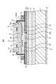
- FIG. 1 is a cross-sectional view showing the structure of a GaN-based HEMT according to the first embodiment.
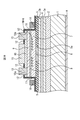
- FIG. 2 is a diagram showing an example of a layout of a structure in which a plurality of GaN-based HEMTs are integrated.
- FIG. 3 is a diagram illustrating another example of a layout of a structure in which a plurality of GaN-based HEMTs are integrated.
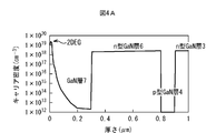
- FIG. 4A is a graph showing the carrier density distribution below the gate electrode 15 when the GaN-based HEMT is off.
- FIG. 4B is a graph showing a carrier density distribution below the gate electrode 15 when the GaN-based HEMT is on.
- FIG. 5A is a cross-sectional view showing the method for manufacturing the GaN-based HEMT according to the first embodiment.
- FIG. 5B is a cross-sectional view showing a method for manufacturing the GaN-based HEMT, following FIG. 5A.
- FIG. 5C is a cross-sectional view showing a method for manufacturing the GaN-based HEMT, following FIG. 5B.
- FIG. 5D is a cross-sectional view illustrating a method for manufacturing the GaN-based HEMT, following FIG. 5C.
- FIG. 5E is a cross-sectional view illustrating a method for manufacturing the GaN-based HEMT, following FIG. 5D.
- FIG. 5A is a cross-sectional view showing the method for manufacturing the GaN-based HEMT according to the first embodiment.
- FIG. 5B is a cross-sectional view showing a method for manufacturing the GaN-based HEMT, following FIG. 5A.
- FIG. 5C is a cross-sectional
- FIG. 5F is a cross-sectional view illustrating a method for manufacturing the GaN-based HEMT, following FIG. 5E.
- FIG. 5G is a cross-sectional view illustrating a method for manufacturing the GaN-based HEMT, following FIG. 5F.
- FIG. 5H is a cross-sectional view illustrating a method for manufacturing the GaN-based HEMT, following FIG. 5G.
- FIG. 5I is a cross-sectional view illustrating a method for manufacturing the GaN-based HEMT, following FIG. 5H.
- FIG. 5J is a cross-sectional view illustrating a method for manufacturing the GaN-based HEMT, following FIG. 5I.
- FIG. 5I is a cross-sectional view illustrating a method for manufacturing the GaN-based HEMT, following FIG. 5I.
- FIG. 5K is a cross-sectional view illustrating a method for manufacturing the GaN-based HEMT, following FIG. 5J.
- FIG. 5L is a cross-sectional view showing a method for manufacturing the GaN-based HEMT, following FIG. 5K.
- FIG. 5M is a cross-sectional view illustrating a method for manufacturing the GaN-based HEMT following FIG. 5L.
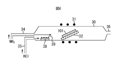
- FIG. 6 is a diagram illustrating a configuration of the HVPE apparatus.
- FIG. 7 is a diagram showing the configuration of the MOCVD apparatus.
- FIG. 8 is a cross-sectional view showing the structure of a GaN-based HEMT according to the second embodiment.
- FIG. 9 is a cross-sectional view showing the structure of a GaN-based HEMT according to the third embodiment.
- FIG. 10 is a cross-sectional view showing the structure of a GaN-based HEMT according to the fourth embodiment.
- FIG. 11 is a cross-sectional view showing the structure of a GaN-based HEMT according to the fifth embodiment.
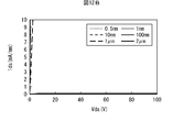
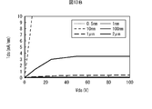
- FIG. 12A is a graph showing IV characteristics during the off operation of the GaN-based HEMT according to the first embodiment.
- FIG. 12B is a graph showing IV characteristics at the time of on-operation of the GaN-based HEMT according to the first embodiment.
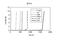
- FIG. 13A is a graph showing an IV characteristic during an off operation of the GaN-based HEMT according to the second embodiment.
- FIG. 13B is a graph showing IV characteristics at the time of on operation of the GaN-based HEMT according to the second embodiment.
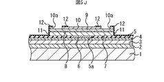
- FIG. 1 is a cross-sectional view showing the structure of a GaN-based HEMT according to the first embodiment.
- an AlN layer 2 and an n-type GaN layer 3 are formed on a substrate 1.
- the substrate 1 is, for example, an n-type silicon single crystal substrate.
- the thickness of the AlN layer 2 is about 1 ⁇ m to 10 ⁇ m.
- the n-type GaN layer 3 is doped with Si by about 1 ⁇ 10 17 cm ⁇ 3 to 1 ⁇ 10 20 cm ⁇ 3 and has a thickness of about 1 ⁇ m to 10 ⁇ m.
- a p-type GaN layer 4 is formed on the n-type GaN layer 3 as a current control layer (second compound semiconductor layer).
- the p-type GaN layer 4 is doped with about 1 ⁇ 10 17 cm ⁇ 3 to about 1 ⁇ 10 20 cm ⁇ 3 of Mg, and the thickness is preferably about 1 nm to 1 ⁇ m, for example. This is because if the thickness is less than 1 nm, sufficient breakdown voltage cannot be obtained, and if it is greater than 1 ⁇ m, the on-state current density decreases due to an increase in on-resistance.
- a silicon oxide film 5 having an opening 5a is formed on the p-type GaN layer 4 as a current confinement layer (current block layer).
- the planar shape of the opening 5a serving as a current passage region is, for example, a rectangle having vertical and horizontal lengths of 0.5 ⁇ m and 500 ⁇ m, respectively.
- the thickness of the silicon oxide film 5 is about 10 nm to 1000 nm.
- n-type GaN layer 6 is formed in the opening 5a. Similar to the n-type GaN layer 3, the n-type GaN layer 6 is doped with Si by about 1 ⁇ 10 17 cm ⁇ 3 to 1 ⁇ 10 19 cm ⁇ 3 .
- a non-doped GaN layer 7, a non-doped AlGaN layer 8, an n-type AlGaN layer 9, and an n-type GaN layer 10 are formed on the silicon oxide film 5 and the n-type GaN layer 6, and an element isolation trench is formed in these. 11 is formed.
- the thickness of the GaN layer 7 is about 0.05 ⁇ m to 5 ⁇ m, and the GaN layer 7 functions as an electron transit layer.
- the thickness of the AlGaN layer 8 is about 1 nm to 20 nm.
- the n-type AlGaN layer 9 is doped with Si by about 1 ⁇ 10 17 cm ⁇ 3 to 1 ⁇ 10 19 cm ⁇ 3 and has a thickness of about 5 nm to 50 nm.
- the n-type AlGaN layer 9 functions as an electron supply layer that supplies electrons to the GaN layer 7 (electron transit layer), and the AlGaN layer 8 includes the GaN layer 7 (electron transit layer) and the n-type AlGaN layer 9 (electron supply layer). ) Function as a spacer layer that is separated from each other. Since the AlGaN layer 8 has a wide band gap, a deep potential well is formed in the vicinity of the interface between the GaN layer 7 and the AlGaN layer 8, and a two-dimensional electron gas 2DEG is generated there.
- the n-type GaN layer 10 is doped with Si by about 1 ⁇ 10 17 cm ⁇ 3 to 1 ⁇ 10 19 cm ⁇ 3 and has a thickness of about 1 nm to 20 nm.
- a silicon nitride film 12 is formed on the n-type GaN layer 10.
- an opening for a gate electrode is formed at the center of the silicon nitride film 12, and an opening for a source electrode surrounding the opening is formed.
- an opening 10 a that matches the opening for the source electrode of the silicon nitride film 12 is formed.
- a gate electrode 15 is formed in the opening for the gate electrode of the silicon nitride film 12, and a source electrode 13 is formed in the opening for the source electrode of the silicon nitride film 12 and the opening 10 a of the n-type GaN layer 10. ing.
- a drain electrode 14 is formed on the back surface of the substrate 1. Further, a control electrode 16 for controlling the potential of the p-type GaN layer 4 is formed on the silicon oxide film 5 in the element isolation trench 11.
- GaN-based HEMT is configured. Further, such GaN-based HEMTs are provided so as to be arranged in two directions orthogonal to each other via the element isolation trench 11 as shown in FIG. Further, such a GaN-based HEMT may be provided so as to be arranged in one direction via the element isolation trench 11 as shown in FIG.
- the potentials of the gate electrode 15 and the control electrode 16 are made equal to the potential of the source electrode 13.
- the conductivity type of the p-type GaN layer 4 is p-type, the band of the conduction band is increased, and the probability of existence of electrons is extremely small.
- a voltage of, for example, 1V is applied to the gate electrode 15 and a predetermined voltage, for example, a voltage of, for example, 5V is applied to the control electrode 16 in order to increase the current value.
- a current flows through the p-type GaN layer 4 and the amount of current can be controlled by the gate electrode 15. The normally-off operation will be described in detail next.
- the current collapse phenomenon in which the on-resistance changes during operation is suppressed by the action of the n-type GaN layer 10 and the silicon nitride film 12.
- FIG. 4A is a graph showing a carrier density distribution below the gate electrode 15 when the GaN-based HEMT (p-type GaN layer 4 thickness: 100 nm) is off.
- the carrier density decreases in the GaN layer 7 along with the depth, and the carrier density increases in the n-type GaN layer 6.
- the carrier density in the p-type GaN layer 4 current control layer
- the carrier density in the n-type GaN layer 3 suddenly increases again. Due to such carrier density distribution, no current flows between the source electrode 16 and the drain electrode 14 even when a voltage is applied to the gate electrode 15.
- FIG. 4B is a graph showing a carrier density distribution below the gate electrode 15 when the GaN-based HEMT (p-type GaN layer 4 thickness: 100 nm) is on. As shown in FIG. 4B, when on, the carrier density of the p-type GaN layer 4 is significantly higher than when off due to the influence of the voltage applied to the control electrode 16. Therefore, when a predetermined voltage is applied to the gate electrode 15, a current flows between the source electrode 16 and the drain electrode 14.
- 5A to 5M are cross-sectional views showing the method of manufacturing the GaN-based HEMT according to the first embodiment in the order of steps.
- halogen vapor phase epitaxy HVPE is formed on a substrate 1.
- the AlN layer 2 is formed by the phase epitaxy method.
- FIG. 6 is a diagram illustrating a configuration of the HVPE apparatus.
- a high frequency coil 31 for induction heating is wound around a quartz reaction tube 30, and a carbon susceptor 32 for placing the substrate 101 is disposed therein.
- Two gas introduction pipes 34 and 35 are connected to the upstream end (the left end in FIG. 6) of the reaction tube 30, and 1 is connected to the downstream end (the right end in FIG. 6) of the reaction tube 30.
- a gas exhaust pipe 36 is connected.
- a boat 38 is arranged on the upstream side of the susceptor 32 in the reaction tube 30, and a group 39 element source 39 of a compound to be grown is accommodated therein.
- the source 39 is Al, for example, when an AlN layer is crystal-grown.
- Ammonia (NH 3 ) gas is introduced from the gas introduction pipe 34 as the N source gas, and hydrogen chloride (HCl) gas is introduced from the gas introduction pipe 35.
- the HCl gas reacts with the group III source 39 in the boat 38 to generate a group III element chloride (such as AlCl) as the source gas.
- Source gas (AlCl gas or the like) and NH 3 gas are conveyed onto the substrate 101 and react on the surface of the substrate 101 to grow an AlN layer or the like. Excess gas is discharged from the gas discharge pipe 36 to the detoxification tower.
- the source 39 for crystal growth of the GaN layer is Ga
- the source gas of the group III element chloride is GaCl.
- the conditions for forming the AlN layer 2 are set as follows, for example. Pressure: normal pressure HCl gas flow rate: 100 ccm (100 cm 3 / min), NH 3 gas flow rate: 10 lm (10 liters / min), Temperature: 1100 ° C.
- an organic chemical vapor deposition (MOCVD) is formed on the AlN layer 2.
- MOCVD organic chemical vapor deposition
- the n-type GaN layer 3 is formed by a deposition method.
- FIG. 7 is a diagram showing the configuration of the MOCVD apparatus.
- a high frequency coil 41 is disposed around the quartz reaction tube 40, and a carbon susceptor 42 for placing the substrate 101 is disposed inside the reaction tube 40.
- Two gas introduction pipes 44 and 45 are connected to the upstream end of the reaction tube 40 (the left end portion in FIG. 7), and a compound source gas is supplied.
- NH 3 gas is introduced from the gas introduction pipe 44 as an N source gas
- organic substances such as trimethylaluminum (TMA), trimethylgallium (TMA), and trimethylindium (TMI) are used as a group III element source gas from the gas introduction pipe 45.
- Group III compound raw material is introduced.
- Crystal growth is performed on the substrate 101, and excess gas is discharged from the gas discharge pipe 46 to the detoxification tower.
- the gas discharge pipe 46 is connected to a vacuum pump, and the discharge port of the vacuum pump is connected to a detoxification tower.
- the MOCVD apparatus is used to form not only the n-type GaN layer 3 but also the p-type GaN layer 4 and the like.
- the conditions for forming the n-type GaN layer 3 are set as follows, for example. Trimethylgallium (TMG) flow rate: 0-50 sccm, Trimethylaluminum (TMA) flow rate: 0-50 sccm, Trimethylindium (TMI) flow rate: 0-50 sccm, Ammonia (NH 3 ) flow rate: 20 slm, n-type impurity: silane (SiH 4 ), Pressure: 100 Torr, Temperature: 1100 ° C.
- TMG Trimethylgallium
- TMA Trimethylaluminum
- TMI Trimethylindium
- Ammonia (NH 3 ) flow rate 20 slm
- n-type impurity silane (SiH 4 )
- Pressure 100 Torr
- Temperature 1100 ° C.
- the conditions for forming the p-type GaN layer 4 and the like are set as follows, for example. Trimethylgallium (TMG) flow rate: 0-50 sccm, Trimethylaluminum (TMA) flow rate: 0-50 sccm, Trimethylindium (TMI) flow rate: 0-50 sccm, Ammonia (NH 3 ) flow rate: 20 slm, p-type impurities: biscyclopentadienyl magnesium (Cp2Mg), Pressure: 100 Torr, Temperature: 1100 ° C.
- TMG Trimethylgallium
- TMA Trimethylaluminum
- TMI Trimethylindium
- Ammonia (NH 3 ) flow rate 20 slm
- p-type impurities biscyclopentadienyl magnesium (Cp2Mg)
- Pressure 100 Torr
- Temperature 1100 ° C.
- the GaN layer is difficult to grow on it. For this reason, it is preferable to form an AlGaN layer (not shown) containing 10 atomic% (at%) of Al in the initial stage of forming the n-type GaN layer 3.
- a p-type GaN layer 4 (current control layer) is formed on the n-type GaN layer 3 by MOCVD as shown in FIG. 5C.
- a silicon oxide film 5 (current confinement layer) having an opening 5 a is formed on the p-type GaN layer 4.
- a silicon oxide film is formed on the entire surface, and a resist pattern exposing a region where an opening 5a is to be formed is formed thereon, and this resist pattern is used as a mask.
- the silicon oxide film may be etched. Thereafter, the resist pattern is removed.
- an n-type GaN layer 6 is formed in the opening 5a by MOCVD.
- the n-type GaN layer 6 grows in the thickness direction on the p-type GaN layer 4 exposed from the opening 5a by selective growth, and does not grow in the thickness direction on the silicon oxide film 5.
- a non-doped GaN layer 7 (electron transit layer) is formed on the silicon oxide film 5 and the n-type GaN layer 6 by MOCVD.
- the GaN layer 7 grows in the thickness direction on the n-type GaN layer 6 and grows laterally from the portion grown in the thickness direction.
- a non-doped AlGaN layer 8, an n-type AlGaN layer 9, and an n-type GaN layer 10 are formed on the GaN layer 7 in this order by the MOCVD method.
- element isolation grooves 11 are formed in the n-type GaN layer 10, the n-type AlGaN layer 9, the AlGaN layer 8, and the GaN layer 7 by recess etching.
- a silicon nitride film 12 is formed on the entire surface of the substrate 1 by plasma CVD, and an opening for a gate electrode and an opening for a source electrode are formed in the silicon nitride film 12. .
- selective etching using SF 6 gas is performed using the resist pattern as a mask.
- an opening 10a is formed by performing time-controlled etching using chlorine gas on the portion of the n-type GaN layer 10 exposed from the opening for the source electrode. To do.
- the source electrode 13 is formed in the opening for the source electrode of the silicon nitride film 12 and the opening 10a of the n-type GaN layer 10 by, for example, a lift-off method.
- a Ta film is formed, and an Al film is formed thereon.
- a surface protective layer 19 is formed on the entire surface of the substrate 1 and the front and back of the substrate 1 are reversed. Then, the thickness of the substrate 1 is set to a predetermined thickness by polishing the back surface of the substrate 1 as necessary. Then, the drain electrode 14 is formed on the entire back surface of the substrate 1.
- the gate electrode 15 is formed in the opening for the gate electrode of the silicon nitride film 12 by, for example, the lift-off method, and the control electrode 16 is formed on the exposed silicon nitride film 5.
- the gate electrode 15 and the control electrode 16 a Ni film is formed, and an Au film is formed thereon.
- a GaN-based HEMT is formed. Thereafter, a passivation film, an external electrode, and the like are formed as necessary to complete the semiconductor device in which the GaN-based HEMT is integrated.
- FIG. 8 is a cross-sectional view showing the structure of a GaN-based HEMT according to the second embodiment.
- an aluminum nitride film (AlN film) 22 having an opening 22a is provided.
- the n-type GaN layer 6 and the GaN layer 7 are in direct contact with the silicon oxide film 5, but in the second embodiment, the n-type GaN layer 6, the GaN layer 7, and the aluminum nitride film.
- An n-type AlGaN layer 21 is formed between them.
- the n-type AlGaN layer 21 is doped with Si by about 1.0 ⁇ 10 17 cm ⁇ 3 to 1.0 ⁇ 10 19 cm ⁇ 3 and has a thickness of about 1 nm to 50 nm.
- Other configurations are the same as those of the first embodiment.
- a fixed negative charge is generated near the interface between the GaN layer 7 and the n-type AlGaN layer 21.
- This charge is a piezo charge generated due to the difference in lattice constant between GaN and AlGaN.
- repelling this negative charge electrons are less likely to be present in the current confinement (opening 22a), and the current in the electron confinement is significantly reduced.
- a positive voltage is applied to the control electrode 16
- the potential of the p-type GaN layer 4 rises, and electrons are first present in the electron confinement portion, and current flows. As described above, if no voltage is applied to the control electrode 16, no current flows through the current confinement portion, and if a voltage is applied, the current flows.
- the normally-off operation is more reliable. Also, a two-dimensional electron gas is generated near the interface between the n-type GaN layer 6 and the n-type AlGaN layer 21, and a current also flows through that portion. For this reason, the on-resistance during operation is reduced.
- FIG. 9 is a cross-sectional view showing the structure of a GaN-based HEMT according to the third embodiment.
- the silicon oxide film 5 and the n-type GaN layer 6 are formed in contact with the n-type GaN layer 3, and the p-type GaN layer 4 is formed on the silicon oxide film 5 and the n-type GaN layer 6. ing. That is, the stacking relationship between the p-type GaN layer 4 and the combination of the silicon oxide film 5 and the n-type GaN layer 6 is opposite to that in the first embodiment. Other configurations are the same as those of the first embodiment.
- the same effect as that of the first embodiment can also be obtained by the third embodiment.
- the third embodiment since the p-type GaN layer 4 is close to the 2DEG region, the depletion layer extends to the 2DEG region, and the off-current can be reduced.
- FIG. 10 is a cross-sectional view showing the structure of a GaN-based HEMT according to the fourth embodiment.
- n-type GaN layers 3a and 3b are provided instead of the n-type GaN layer 3, and the p-type GaN layer 4 is provided therebetween. That is, the n-type GaN layer 3 a is formed on the AlN layer 2, the p-type GaN layer 4 is formed on the n-type GaN layer 3 a, and the n-type GaN layer 3 b is formed on the p-type GaN layer 4.
- Other configurations are the same as those of the first embodiment.
- the same effect as that of the first embodiment can also be obtained by the fourth embodiment.
- the fourth embodiment since the p-type GaN layer 4 is not etched, the crystallinity thereof is easily maintained. As a result, the on-resistance can be further reduced, and the current blocking capability at the off time can be improved.
- the portion of the n-type GaN layer 3b located between the control electrode 16 and the p-type GaN layer 4 is removed. It is preferable. However, even if the n-type GaN layer 3b remains, since the n-type GaN layer 3b is very thin compared to the area of the control electrode 16, it is possible to apply a voltage from the control electrode 16 to the p-type GaN layer 4. It is.
- FIG. 11 is a cross-sectional view showing the structure of a GaN-based HEMT according to the fifth embodiment.
- the n-type GaN layer 6 is formed not only in the opening 5 a but also on the silicon oxide film 5.
- the thickness of the n-type GaN layer 6 in this embodiment is about 500 nm.
- the n-type GaN layer 6 grows in the thickness direction in the opening 5a, and then grows laterally from the portion grown in the thickness direction.
- Other configurations are the same as those of the first embodiment.
- the same effect as that of the first embodiment can also be obtained by the fifth embodiment.
- the contact area between the 2DEG region and the n-type GaN layer 6 is large, the on-resistance is reduced.
- the n-type GaN layer 6 in the fifth embodiment may be applied to the second to fourth embodiments.
- the material, thickness, impurity concentration, and the like of the substrate 1 and each layer are not particularly limited.
- the substrate 1 in addition to the conductive silicon substrate, a conductive sapphire substrate, a conductive SiC substrate, a conductive GaN substrate, or the like may be used.
- a p-type GaN layer may be used as the current confinement layer (current block layer).
- the etching of the p-type GaN layer is difficult as compared with the etching of the silicon oxide film and the aluminum nitride film, and the pinch-off characteristic tends to be lowered.
- the lattice constant of the sapphire substrate is relatively different from the lattice constant of the nitride-based compound semiconductor layer, dislocations are likely to occur in the compound semiconductor layer, and the crystallinity tends to be low. For this reason, it becomes difficult to obtain desired characteristics. Therefore, a conductive semiconductor substrate is preferable as the substrate, and a silicon oxide film or an aluminum nitride film is preferable as the current confinement layer (current blocking layer).
- control electrode 16 and the p-type GaN layer 4 may be in direct contact.
- FIG. 12A, 12B, 13A, and 13B show the characteristics of the GaN-based HEMT according to the first embodiment during the off operation and during the on operation, respectively.
- FIGS. 13A and 13B show the characteristics of the GaN-based HEMT according to the third embodiment during the off operation and during the on operation, respectively.
- the horizontal axis indicates the voltage (Vds) applied between the source electrode 13 and the drain electrode 14, and the vertical axis indicates the density (Ids) of the current flowing between the source electrode 13 and the drain electrode 14. Indicates.
- the normally-off operation is confirmed if the thickness of the p-type GaN layer 4 is 1 nm, 10 nm, 100 nm, or 1 ⁇ m.
- a current flows at an appropriate density during the on-operation.
- the normally-off operation was not confirmed in the sample with the p-type GaN layer 4 having a thickness of 0.5 nm. Further, as shown in FIGS. 12A and 13A, as shown in FIGS.
- the current density at the on time was very low. Therefore, if the thickness of the p-type GaN layer 4 is 1 nm or more and 1 ⁇ m or less, the p-type GaN layer 4 can exhibit sufficient current blocking characteristics when turned off and can have a sufficiently low on-resistance. it is conceivable that.
- the GaN-based HEMT according to the first embodiment has a high withstand voltage
- the GaN-based HEMT according to the third embodiment has a high resistance during on-operation. This is because in the GaN-based HEMT according to the third embodiment, the p-type GaN layer 4 is formed after the selective growth of the n-type GaN layer 6, and there is a defect in the periphery of the p-type GaN layer 4. This is thought to be due to a relatively large increase.
Landscapes
- Engineering & Computer Science (AREA)
- Microelectronics & Electronic Packaging (AREA)
- Power Engineering (AREA)
- Physics & Mathematics (AREA)
- Condensed Matter Physics & Semiconductors (AREA)
- General Physics & Mathematics (AREA)
- Computer Hardware Design (AREA)
- Ceramic Engineering (AREA)
- Manufacturing & Machinery (AREA)
- Junction Field-Effect Transistors (AREA)
Abstract
Description
先ず、第1の実施形態について説明する。図1は、第1の実施形態に係るGaN系HEMTの構造を示す断面図である。
phase epitaxy)法によりAlN層2を形成する。
圧力:常圧、
HClガスの流量:100ccm(100cm3/min)、
NH3ガスの流量:10lm(10リットル/min)、
温度:1100℃。
deposition)法によりn型GaN層3を形成する。
トリメチルガリウム(TMG)の流量:0~50sccm、
トリメチルアルミニウム(TMA)の流量:0~50sccm、
トリメチルインジウム(TMI)の流量:0~50sccm、
アンモニア(NH3)の流量:20slm、
n型不純物:シラン(SiH4)、
圧力:100Torr、
温度:1100℃。
トリメチルガリウム(TMG)の流量:0~50sccm、
トリメチルアルミニウム(TMA)の流量:0~50sccm、
トリメチルインジウム(TMI)の流量:0~50sccm、
アンモニア(NH3)の流量:20slm、
p型不純物:ビスシクロペンタディエニルマグネシウム(Cp2Mg)、
圧力:100Torr、
温度:1100℃。
次に、第2の実施形態について説明する。図8は、第2の実施形態に係るGaN系HEMTの構造を示す断面図である。
次に、第3の実施形態について説明する。図9は、第3の実施形態に係るGaN系HEMTの構造を示す断面図である。
次に、第4の実施形態について説明する。図10は、第4の実施形態に係るGaN系HEMTの構造を示す断面図である。
次に、第5の実施形態について説明する。図11は、第5の実施形態に係るGaN系HEMTの構造を示す断面図である。
Claims (18)
- 第1の導電型の第1の化合物半導体層と、
前記第1の化合物半導体層の上方に形成された電子走行層と、
前記電子走行層の上方に形成された電子供給層と、
前記電子供給層の上方に形成されたゲート電極及びソース電極と、
前記第1の化合物半導体層の下方に形成されたドレイン電極と、
前記電子走行層と前記ドレイン電極との間に形成された前記第1の導電型と異なる第2の導電型の第2の化合物半導体層と、
前記第2の化合物半導体層の電位を制御する制御手段と、
を有することを特徴とする化合物半導体装置。 - 前記電子走行層と前記ドレイン電極との間に形成され、開口部を備えた電流狭窄層を有することを特徴とする請求項1に記載の化合物半導体装置。
- 前記電子走行層と前記第2の化合物半導体層との間に形成された前記第1の導電型の第3の化合物半導体層を有することを特徴とする請求項1に記載の化合物半導体装置。
- 前記開口部内に形成された前記第1の導電型の第3の化合物半導体層を有することを特徴とする請求項2に記載の化合物半導体装置。
- 前記第2の化合物半導体層は、前記第1の化合物半導体層と前記電子走行層との間に位置していることを特徴とする請求項1に記載の化合物半導体装置。
- 前記第2の化合物半導体層は、前記第1の化合物半導体層と前記電流狭窄層との間に位置していることを特徴とする請求項2に記載の化合物半導体装置。
- 前記第2の化合物半導体層は、前記電流狭窄層と前記電子走行層との間に位置していることを特徴とする請求項2に記載の化合物半導体装置。
- 前記電流狭窄層は、AlN層であり、
前記電子走行層は、n型GaN層であり、
前記電流狭窄層と前記電子走行層との間に形成されたn型AlGaN層を有することを特徴とする請求項2に記載の化合物半導体装置。 - 前記第1の化合物半導体層と前記ドレイン電極との間に位置する導電性基板を有することを特徴とする請求項1に記載の化合物半導体装置。
- 前記第2の化合物半導体層の厚さは、1nm乃至1μmであることを特徴とする請求項1に記載の化合物半導体装置。
- 第1の導電型の第1の化合物半導体層上方に、前記第1の導電型と異なる第2の導電型の第2の化合物半導体層を形成する工程と、
前記第2の化合物半導体層の上方に電子走行層を形成する工程と、
前記電子走行層上に電子供給層を形成する工程と、
前記電子供給層の上方にゲート電極及びソース電極を形成する工程と、
前記第1の化合物半導体層の下方にドレイン電極を形成する工程と、
前記第2の化合物半導体層の電位を制御する制御手段を形成する工程と、
を有することを特徴とする化合物半導体装置の製造方法。 - 前記電子走行層を形成する工程の前に、開口部を備えた電流狭窄層を前記第1の化合物半導体層の上方に形成する工程を有することを特徴とする請求項11に記載の化合物半導体装置の製造方法。
- 前記第2の化合物半導体層を形成する工程と前記電子走行層を形成する工程との間に、前記第2の化合物半導体層の上方に前記第1の導電型の第3の化合物半導体層を形成する工程を有することを特徴とする請求項11に記載の化合物半導体装置の製造方法。
- 前記開口部内に、前記第1の導電型の第3の化合物半導体層を形成する工程を有することを特徴とする請求項12に記載の化合物半導体装置の製造方法。
- 前記電流狭窄層を形成する工程を、前記第2の化合物半導体層を形成する工程と前記電子走行層を形成する工程との間に行うことを特徴とする請求項12に記載の化合物半導体装置の製造方法。
- 前記電流狭窄層を形成する工程を、前記第2の化合物半導体層を形成する工程の前に行うことを特徴とする請求項12に記載の化合物半導体装置の製造方法。
- 前記電流狭窄層として、AlN層を形成し、
前記電子走行層として、n型GaN層を形成し、
前記電流狭窄層を形成する工程と前記電子走行層を形成する工程との間に、前記電流狭窄層上にn型AlGaN層を形成する工程を有することを特徴とする請求項12に記載の化合物半導体装置の製造方法。 - 前記第2の化合物半導体層の厚さを1nm乃至1μmとすることを特徴とする請求項11に記載の化合物半導体装置の製造方法。
Priority Applications (6)
| Application Number | Priority Date | Filing Date | Title |
|---|---|---|---|
| CN200880131746.9A CN102197468B (zh) | 2008-10-29 | 2008-10-29 | 化合物半导体器件及其制造方法 |
| EP08877732.1A EP2346071B1 (en) | 2008-10-29 | 2008-10-29 | Compound semiconductor device and method for manufacturing the same |
| KR1020117009163A KR101167651B1 (ko) | 2008-10-29 | 2008-10-29 | 화합물 반도체 장치 및 그 제조 방법 |
| JP2010535561A JP5533661B2 (ja) | 2008-10-29 | 2008-10-29 | 化合物半導体装置及びその製造方法 |
| PCT/JP2008/069676 WO2010050021A1 (ja) | 2008-10-29 | 2008-10-29 | 化合物半導体装置及びその製造方法 |
| US13/091,322 US8618577B2 (en) | 2008-10-29 | 2011-04-21 | Compound semiconductor device and manufacturing method thereof |
Applications Claiming Priority (1)
| Application Number | Priority Date | Filing Date | Title |
|---|---|---|---|
| PCT/JP2008/069676 WO2010050021A1 (ja) | 2008-10-29 | 2008-10-29 | 化合物半導体装置及びその製造方法 |
Related Child Applications (1)
| Application Number | Title | Priority Date | Filing Date |
|---|---|---|---|
| US13/091,322 Continuation US8618577B2 (en) | 2008-10-29 | 2011-04-21 | Compound semiconductor device and manufacturing method thereof |
Publications (1)
| Publication Number | Publication Date |
|---|---|
| WO2010050021A1 true WO2010050021A1 (ja) | 2010-05-06 |
Family
ID=42128400
Family Applications (1)
| Application Number | Title | Priority Date | Filing Date |
|---|---|---|---|
| PCT/JP2008/069676 WO2010050021A1 (ja) | 2008-10-29 | 2008-10-29 | 化合物半導体装置及びその製造方法 |
Country Status (6)
| Country | Link |
|---|---|
| US (1) | US8618577B2 (ja) |
| EP (1) | EP2346071B1 (ja) |
| JP (1) | JP5533661B2 (ja) |
| KR (1) | KR101167651B1 (ja) |
| CN (1) | CN102197468B (ja) |
| WO (1) | WO2010050021A1 (ja) |
Cited By (1)
| Publication number | Priority date | Publication date | Assignee | Title |
|---|---|---|---|---|
| CN102468331A (zh) * | 2010-11-02 | 2012-05-23 | 富士通株式会社 | 半导体器件及其制造方法 |
Families Citing this family (21)
| Publication number | Priority date | Publication date | Assignee | Title |
|---|---|---|---|---|
| US9029866B2 (en) | 2009-08-04 | 2015-05-12 | Gan Systems Inc. | Gallium nitride power devices using island topography |
| US9818857B2 (en) | 2009-08-04 | 2017-11-14 | Gan Systems Inc. | Fault tolerant design for large area nitride semiconductor devices |
| US9064947B2 (en) | 2009-08-04 | 2015-06-23 | Gan Systems Inc. | Island matrixed gallium nitride microwave and power switching transistors |
| EP2559064A4 (en) * | 2010-04-13 | 2018-07-18 | GaN Systems Inc. | High density gallium nitride devices using island topology |
| JP5919626B2 (ja) * | 2011-02-25 | 2016-05-18 | 富士通株式会社 | 化合物半導体装置及びその製造方法 |
| JP5784441B2 (ja) * | 2011-09-28 | 2015-09-24 | トランスフォーム・ジャパン株式会社 | 半導体装置及び半導体装置の製造方法 |
| JP2013197315A (ja) * | 2012-03-19 | 2013-09-30 | Fujitsu Ltd | 半導体装置及び半導体装置の製造方法 |
| JP5895651B2 (ja) * | 2012-03-28 | 2016-03-30 | 富士通株式会社 | 化合物半導体装置及びその製造方法 |
| JP2014072397A (ja) * | 2012-09-28 | 2014-04-21 | Fujitsu Ltd | 化合物半導体装置及びその製造方法 |
| JP2014146646A (ja) * | 2013-01-28 | 2014-08-14 | Fujitsu Ltd | 半導体装置 |
| KR102036349B1 (ko) * | 2013-03-08 | 2019-10-24 | 삼성전자 주식회사 | 고 전자이동도 트랜지스터 |
| KR102055839B1 (ko) | 2013-03-08 | 2019-12-13 | 삼성전자주식회사 | 질화계 반도체 소자 |
| KR102065114B1 (ko) * | 2013-03-14 | 2020-01-10 | 삼성전자주식회사 | 파워 소자의 전류 붕괴를 감소시키는 구동방법 |
| JP6174874B2 (ja) * | 2013-03-15 | 2017-08-02 | ルネサスエレクトロニクス株式会社 | 半導体装置 |
| JP6070846B2 (ja) * | 2013-07-31 | 2017-02-01 | 富士電機株式会社 | 半導体装置の製造方法および半導体装置 |
| JP2015032744A (ja) * | 2013-08-05 | 2015-02-16 | 株式会社東芝 | 半導体装置および半導体装置の製造方法 |
| FR3011981B1 (fr) * | 2013-10-11 | 2018-03-02 | Centre National De La Recherche Scientifique - Cnrs - | Transistor hemt a base d'heterojonction |
| FR3012049B1 (fr) | 2013-10-17 | 2022-02-25 | Abc Membranes | Fabrication d'une membrane de filtration |
| US9590048B2 (en) * | 2013-10-31 | 2017-03-07 | Infineon Technologies Austria Ag | Electronic device |
| FR3030114B1 (fr) | 2014-12-15 | 2018-01-26 | Centre National De La Recherche Scientifique - Cnrs - | Transistor hemt |
| CN106449406B (zh) * | 2016-05-30 | 2020-05-12 | 湖南理工学院 | 一种垂直结构GaN基增强型场效应晶体管及其制造方法 |
Citations (4)
| Publication number | Priority date | Publication date | Assignee | Title |
|---|---|---|---|---|
| JPS6191965A (ja) * | 1984-10-12 | 1986-05-10 | Hitachi Ltd | 半導体装置 |
| JPH0730073A (ja) * | 1993-05-12 | 1995-01-31 | Semiconductor Res Found | 半導体デバイス及びその製造方法 |
| JP2006140368A (ja) | 2004-11-15 | 2006-06-01 | Toyota Central Res & Dev Lab Inc | 半導体装置とその製造方法 |
| JP2008218813A (ja) * | 2007-03-06 | 2008-09-18 | Toyota Central R&D Labs Inc | 半導体装置とその製造方法 |
Family Cites Families (11)
| Publication number | Priority date | Publication date | Assignee | Title |
|---|---|---|---|---|
| EP0631326B1 (en) * | 1993-05-12 | 1999-02-24 | Zaidan Hojin Handotai Kenkyu Shinkokai | Semiconductor memory device and method of manufacturing same |
| JP2000106371A (ja) * | 1998-07-31 | 2000-04-11 | Denso Corp | 炭化珪素半導体装置の製造方法 |
| US7084441B2 (en) * | 2004-05-20 | 2006-08-01 | Cree, Inc. | Semiconductor devices having a hybrid channel layer, current aperture transistors and methods of fabricating same |
| JP4916671B2 (ja) | 2005-03-31 | 2012-04-18 | 住友電工デバイス・イノベーション株式会社 | 半導体装置 |
| US8575651B2 (en) * | 2005-04-11 | 2013-11-05 | Cree, Inc. | Devices having thick semi-insulating epitaxial gallium nitride layer |
| JP4932305B2 (ja) * | 2006-03-30 | 2012-05-16 | 株式会社豊田中央研究所 | Iii族窒化物系化合物半導体素子の製造方法 |
| JP2008021756A (ja) * | 2006-07-12 | 2008-01-31 | Toyota Motor Corp | Iii族窒化物半導体装置 |
| JP5048382B2 (ja) * | 2006-12-21 | 2012-10-17 | 株式会社豊田中央研究所 | 半導体装置とその製造方法 |
| DE112008000410T5 (de) * | 2007-02-16 | 2009-12-24 | Sumitomo Chemical Company, Limited | Epitaxialer Galliumnitridkristall, Verfahren zu dessen Herstellung und Feldeffekttransistor |
| JP5099116B2 (ja) * | 2007-02-27 | 2012-12-12 | 富士通株式会社 | 化合物半導体装置とその製造方法 |
| JP5095253B2 (ja) * | 2007-03-30 | 2012-12-12 | 富士通株式会社 | 半導体エピタキシャル基板、化合物半導体装置、およびそれらの製造方法 |
-
2008
- 2008-10-29 EP EP08877732.1A patent/EP2346071B1/en active Active
- 2008-10-29 JP JP2010535561A patent/JP5533661B2/ja active Active
- 2008-10-29 WO PCT/JP2008/069676 patent/WO2010050021A1/ja active Application Filing
- 2008-10-29 KR KR1020117009163A patent/KR101167651B1/ko active IP Right Grant
- 2008-10-29 CN CN200880131746.9A patent/CN102197468B/zh active Active
-
2011
- 2011-04-21 US US13/091,322 patent/US8618577B2/en active Active
Patent Citations (4)
| Publication number | Priority date | Publication date | Assignee | Title |
|---|---|---|---|---|
| JPS6191965A (ja) * | 1984-10-12 | 1986-05-10 | Hitachi Ltd | 半導体装置 |
| JPH0730073A (ja) * | 1993-05-12 | 1995-01-31 | Semiconductor Res Found | 半導体デバイス及びその製造方法 |
| JP2006140368A (ja) | 2004-11-15 | 2006-06-01 | Toyota Central Res & Dev Lab Inc | 半導体装置とその製造方法 |
| JP2008218813A (ja) * | 2007-03-06 | 2008-09-18 | Toyota Central R&D Labs Inc | 半導体装置とその製造方法 |
Non-Patent Citations (2)
| Title |
|---|
| JAPANESE JOURNAL OF APPLIED PHYSICS, vol. 46, no. 21, 2007, pages L503 - L505 |
| See also references of EP2346071A4 * |
Cited By (1)
| Publication number | Priority date | Publication date | Assignee | Title |
|---|---|---|---|---|
| CN102468331A (zh) * | 2010-11-02 | 2012-05-23 | 富士通株式会社 | 半导体器件及其制造方法 |
Also Published As
| Publication number | Publication date |
|---|---|
| KR101167651B1 (ko) | 2012-07-20 |
| JP5533661B2 (ja) | 2014-06-25 |
| CN102197468B (zh) | 2014-04-02 |
| EP2346071B1 (en) | 2017-04-05 |
| KR20110074557A (ko) | 2011-06-30 |
| CN102197468A (zh) | 2011-09-21 |
| JPWO2010050021A1 (ja) | 2012-03-29 |
| EP2346071A1 (en) | 2011-07-20 |
| US8618577B2 (en) | 2013-12-31 |
| US20110193096A1 (en) | 2011-08-11 |
| EP2346071A4 (en) | 2012-09-12 |
Similar Documents
| Publication | Publication Date | Title |
|---|---|---|
| JP5533661B2 (ja) | 化合物半導体装置及びその製造方法 | |
| JP5099116B2 (ja) | 化合物半導体装置とその製造方法 | |
| US9548376B2 (en) | Method of manufacturing a semiconductor device including a barrier structure | |
| US8735942B2 (en) | Compound semiconductor device and manufacturing method of the same | |
| US8866192B1 (en) | Semiconductor device, high electron mobility transistor (HEMT) and method of manufacturing | |
| JP2007165431A (ja) | 電界効果型トランジスタおよびその製造方法 | |
| JP5566670B2 (ja) | GaN系電界効果トランジスタ | |
| JP2010192633A (ja) | GaN系電界効果トランジスタの製造方法 | |
| JP7013710B2 (ja) | 窒化物半導体トランジスタの製造方法 | |
| JPWO2007122669A1 (ja) | 多結晶SiC基板を有する化合物半導体ウエハ、化合物半導体装置とそれらの製造方法 | |
| JP2005183733A (ja) | 高電子移動度トランジスタ | |
| JP2009170546A (ja) | GaN系電界効果トランジスタ | |
| JP5593673B2 (ja) | 半導体装置及びその製造方法 | |
| JP4748501B2 (ja) | 高電子移動度トランジスタ | |
| CN106910770B (zh) | 氮化镓基反相器芯片及其形成方法 | |
| JP6519920B2 (ja) | 半導体基板の製造方法、及び半導体装置の製造方法 | |
| JP2013149959A (ja) | 窒化物系半導体装置 | |
| JP5534049B2 (ja) | 多結晶SiC基板を有する化合物半導体ウエハ、化合物半導体装置とそれらの製造方法 | |
| JP2006060071A (ja) | GaN系電界効果トランジスタ | |
| JP4924046B2 (ja) | 接合型iii族窒化物トランジスタを作製する方法 | |
| EP3564987A1 (en) | Semiconductor substrate and electronic device |
Legal Events
| Date | Code | Title | Description |
|---|---|---|---|
| WWE | Wipo information: entry into national phase |
Ref document number: 200880131746.9 Country of ref document: CN |
|
| 121 | Ep: the epo has been informed by wipo that ep was designated in this application |
Ref document number: 08877732 Country of ref document: EP Kind code of ref document: A1 |
|
| WWE | Wipo information: entry into national phase |
Ref document number: 2010535561 Country of ref document: JP |
|
| ENP | Entry into the national phase |
Ref document number: 20117009163 Country of ref document: KR Kind code of ref document: A |
|
| REEP | Request for entry into the european phase |
Ref document number: 2008877732 Country of ref document: EP |
|
| WWE | Wipo information: entry into national phase |
Ref document number: 2008877732 Country of ref document: EP |
|
| NENP | Non-entry into the national phase |
Ref country code: DE |