WO2010035624A1 - 固体撮像素子 - Google Patents
固体撮像素子 Download PDFInfo
- Publication number
- WO2010035624A1 WO2010035624A1 PCT/JP2009/065493 JP2009065493W WO2010035624A1 WO 2010035624 A1 WO2010035624 A1 WO 2010035624A1 JP 2009065493 W JP2009065493 W JP 2009065493W WO 2010035624 A1 WO2010035624 A1 WO 2010035624A1
- Authority
- WO
- WIPO (PCT)
- Prior art keywords
- solid
- state imaging
- infrared
- imaging device
- infrared detection
- Prior art date
- Legal status (The legal status is an assumption and is not a legal conclusion. Google has not performed a legal analysis and makes no representation as to the accuracy of the status listed.)
- Ceased
Links
Images



Classifications
-
- G—PHYSICS
- G01—MEASURING; TESTING
- G01V—GEOPHYSICS; GRAVITATIONAL MEASUREMENTS; DETECTING MASSES OR OBJECTS; TAGS
- G01V8/00—Prospecting or detecting by optical means
- G01V8/10—Detecting, e.g. by using light barriers
-
- H—ELECTRICITY
- H04—ELECTRIC COMMUNICATION TECHNIQUE
- H04N—PICTORIAL COMMUNICATION, e.g. TELEVISION
- H04N23/00—Cameras or camera modules comprising electronic image sensors; Control thereof
- H04N23/20—Cameras or camera modules comprising electronic image sensors; Control thereof for generating image signals from infrared radiation only
-
- G—PHYSICS
- G01—MEASURING; TESTING
- G01J—MEASUREMENT OF INTENSITY, VELOCITY, SPECTRAL CONTENT, POLARISATION, PHASE OR PULSE CHARACTERISTICS OF INFRARED, VISIBLE OR ULTRAVIOLET LIGHT; COLORIMETRY; RADIATION PYROMETRY
- G01J5/00—Radiation pyrometry, e.g. infrared or optical thermometry
- G01J2005/0077—Imaging
-
- G—PHYSICS
- G01—MEASURING; TESTING
- G01J—MEASUREMENT OF INTENSITY, VELOCITY, SPECTRAL CONTENT, POLARISATION, PHASE OR PULSE CHARACTERISTICS OF INFRARED, VISIBLE OR ULTRAVIOLET LIGHT; COLORIMETRY; RADIATION PYROMETRY
- G01J5/00—Radiation pyrometry, e.g. infrared or optical thermometry
- G01J5/10—Radiation pyrometry, e.g. infrared or optical thermometry using electric radiation detectors
- G01J5/20—Radiation pyrometry, e.g. infrared or optical thermometry using electric radiation detectors using resistors, thermistors or semiconductors sensitive to radiation, e.g. photoconductive devices
-
- G—PHYSICS
- G01—MEASURING; TESTING
- G01J—MEASUREMENT OF INTENSITY, VELOCITY, SPECTRAL CONTENT, POLARISATION, PHASE OR PULSE CHARACTERISTICS OF INFRARED, VISIBLE OR ULTRAVIOLET LIGHT; COLORIMETRY; RADIATION PYROMETRY
- G01J5/00—Radiation pyrometry, e.g. infrared or optical thermometry
- G01J5/10—Radiation pyrometry, e.g. infrared or optical thermometry using electric radiation detectors
- G01J5/20—Radiation pyrometry, e.g. infrared or optical thermometry using electric radiation detectors using resistors, thermistors or semiconductors sensitive to radiation, e.g. photoconductive devices
- G01J5/22—Electrical features thereof
-
- H—ELECTRICITY
- H10—SEMICONDUCTOR DEVICES; ELECTRIC SOLID-STATE DEVICES NOT OTHERWISE PROVIDED FOR
- H10F—INORGANIC SEMICONDUCTOR DEVICES SENSITIVE TO INFRARED RADIATION, LIGHT, ELECTROMAGNETIC RADIATION OF SHORTER WAVELENGTH OR CORPUSCULAR RADIATION
- H10F30/00—Individual radiation-sensitive semiconductor devices in which radiation controls the flow of current through the devices, e.g. photodetectors
- H10F30/20—Individual radiation-sensitive semiconductor devices in which radiation controls the flow of current through the devices, e.g. photodetectors the devices having potential barriers, e.g. phototransistors
- H10F30/21—Individual radiation-sensitive semiconductor devices in which radiation controls the flow of current through the devices, e.g. photodetectors the devices having potential barriers, e.g. phototransistors the devices being sensitive to infrared, visible or ultraviolet radiation
-
- H—ELECTRICITY
- H10—SEMICONDUCTOR DEVICES; ELECTRIC SOLID-STATE DEVICES NOT OTHERWISE PROVIDED FOR
- H10F—INORGANIC SEMICONDUCTOR DEVICES SENSITIVE TO INFRARED RADIATION, LIGHT, ELECTROMAGNETIC RADIATION OF SHORTER WAVELENGTH OR CORPUSCULAR RADIATION
- H10F39/00—Integrated devices, or assemblies of multiple devices, comprising at least one element covered by group H10F30/00, e.g. radiation detectors comprising photodiode arrays
- H10F39/10—Integrated devices
Definitions
- the present invention relates to an uncooled (thermal) solid-state imaging device for an infrared band.
- infrared sensors that support infrared rays in the 8 ⁇ m to 12 ⁇ m band are used for security cameras and in-vehicle front surveillance cameras because of their high sensitivity to infrared rays emitted from objects near room temperature.
- MEMS Micro-Electro-Mechanical System
- an uncooled (thermal) infrared sensor that senses infrared rays without cooling an element is becoming mainstream.
- a thermal infrared sensor absorbs infrared rays collected by a far-infrared lens (mainly a Ge lens) by pixels that are arrayed on a semiconductor substrate and thermally isolated from the semiconductor substrate.
- the pixel has a configuration in which the heat rise of the pixel is converted into an electric signal by thermoelectric conversion and imaged.
- a thermal infrared sensor capable of reducing the heat capacity of a cell by simplifying a wiring layer and capable of high-speed response has been proposed (for example, see Patent Document 1).
- the heat capacity of the cell is reduced by simplifying the wiring layer, thereby enabling a high-speed response.
- the thermal infrared sensor described in Patent Document 1 cannot quickly and easily determine the position of the subject.
- the thermal infrared sensor described in Patent Document 1 is an image sensor, it is necessary to perform a scanning operation for selecting an output one by one in order and reading out an output signal. Takes time. Therefore, the infrared response speed of the pixel cannot be fully utilized.
- the present invention has been made in consideration of the above circumstances, and an object of the present invention is to provide a solid-state imaging device that can quickly and easily determine the position of a subject.
- a solid-state imaging device includes at least two infrared detection units formed on a semiconductor substrate, electric wiring connecting the at least two infrared detection units in series, and the infrared detection units in series. And a comparator for comparing an intermediate potential of the electric wiring connected to the reference potential set in advance.
- the position of the subject can be determined quickly and easily.
- FIG. 2 is a cross-sectional view of the solid-state imaging device according to the first embodiment cut along a cutting line AA shown in FIG.
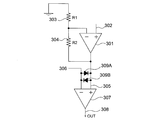
- FIG. 3 is a circuit diagram showing a specific example of a comparator according to the first embodiment.
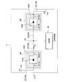
- FIG. 1 shows a plan view of the solid-state imaging device of the present embodiment
- FIG. 2 shows a cross section taken along the cutting line AA shown in FIG.
- the solid-state imaging device 1 according to the present embodiment includes two pixels (infrared detectors) 2A and 2B, and a comparator 30.
- Each pixel 2A, 2B has a cell portion 20 as shown in FIG.
- the cell portion 20 is disposed above a recess (cavity) 14 formed in a surface portion of a semiconductor substrate, for example, a silicon substrate 100, and is supported by support structure portions 221 and 222.
- the cell unit 20 includes a thermoelectric conversion element 21 and an infrared absorption layer 24 that covers the thermoelectric conversion element 21.
- the thermoelectric conversion element 21 is electrically insulated from the infrared absorption layer 24 and electrically connected to connection wirings 2212 and 2221 provided in the support structure portions 221 and 222.
- These connection wirings 2212 and 2221 are covered with insulating films (protective films) 2212 and 2222, respectively.
- the connection wirings 2212 and 2221 are connected to wirings 2312 and 2313 provided on the semiconductor substrate 100, respectively.
- the wirings 2312 and 2313 are covered with insulating films 2311 and 2322, respectively.
- thermoelectric conversion element 21A is connected to connection wirings 221A and 222A provided in the support structure portions 221 and 222.
- the connection wiring 221A is connected to the Vdd power supply 41 via the wiring 2312A provided on the semiconductor substrate 100, and the connection wiring 222A is connected to the comparator 30 via the wiring 2313A provided on the semiconductor substrate 100 and the node 31.
- the thermoelectric conversion element 21B is connected to connection wirings 221B and 222B provided in the support structure portions 221 and 222.
- connection wiring 221B is connected to the comparator 30 via the wiring 2312B provided on the semiconductor substrate 100 and the node 31, and the connection wiring 222B is connected to the Vss power source 42 via the wiring 2313B provided on the semiconductor substrate 100.
- the comparator 30 may be formed on the semiconductor substrate (semiconductor chip) 100 or may be formed outside the semiconductor chip.
- the infrared rays when infrared rays from a subject are incident, the infrared rays are absorbed by the infrared absorption layer 24 of the cell unit 20, and the temperature of the infrared absorption layer 24 is generated by the generated thermal energy. Rises. This change in temperature is converted into an electrical signal by the thermoelectric conversion element 21 and becomes an output of the pixel. Then, the output of the pixel 2A and the pixel 2B is compared by the comparator 30 to detect the position of the subject.
- the solid-state imaging device of the present embodiment is operated in a vacuum, only the support structure portions 221 and 222 have a heat escape path from the cell portion 20. Therefore, the thermal isolation of the cell part 20 is determined by the thermal conductance of the support structure parts 221 and 222, and the longer the support structure part is configured, the more heat insulation is improved. .
- the temperature change ⁇ T of the cell unit 20 due to the thermal energy generated in the infrared absorption layer 24 is As you go up.
- P a is the infrared energy incident on the cell portion 20 (W)
- C th is the heat capacity of the cell (J / K)
- t is the time elapsed after the reception start (s).
- the cell part 20 has a square shape with a side of about 30 ⁇ m and a height of about 4 ⁇ m to 5 ⁇ m.
- the cell part 20 includes two support structure parts for supporting the cell part 20, and the cross section of the protective film of each support structure part is one side. Is about 1 ⁇ m, and the length from the cell portion 20 to the protective film of the connection wiring is about 70 ⁇ m, the thermal time constant is on the order of about 20 msec to 50 msec. The temperature rise of the cell due to infrared reception is It becomes.
- thermoelectric conversion element 21 in order to detect the temperature rise ⁇ T of the cell unit 20, a resistor is used as the thermoelectric conversion element 21 in the present embodiment. Using the property of resistance change with respect to the temperature of the resistor 21, the temperature rise of the cell unit 20 can be extracted as an electric signal.
- the resistance change (temperature resistance coefficient) of the resistor 21 according to the temperature change is dR / dT.
- dR / dT The resistance change (temperature resistance coefficient) of the resistor 21 according to the temperature change.
- TiN titanium nitride
- the resistance change is 150 ⁇ with respect to a change at a temperature of 1 ° C.
- the pixels 2A and 2B are respectively formed at two locations on the semiconductor substrate 100 as shown in FIG. Depending on the position of the subject, one of these pixels 2A, 2B is irradiated with infrared rays. When infrared rays from the subject are irradiated only on the pixel 2A, a temperature change represented by the equation (3) occurs only in the pixel 2A at that time.
- the pixel 2A and the pixel 2B are connected by wiring, and a voltage is applied in series to the pixel 2A and the pixel 2B by the Vdd power source 41 and the Vss power source 42.
- the pixel 2A and the pixel 2B have The current represented by flows. Accordingly, the potential V 31 of the node 31 connected to the wiring 2313A and the connection wiring 2312B is connected, It becomes.
- the comparator 30 sets the node potential V 31 to the threshold voltage V th represented by the following equation (6). Compare with As described above, when the pixel 2A is irradiated with infrared rays, The node potential V 31 is lower than the threshold voltage V th , but conversely, when the pixel 2B is irradiated with infrared rays, This is the reverse of the case described above.
- the input terminal corresponds to the input 302 of the operational amplifier 301.
- the output of the non-inverting amplifier circuit 301 is input to the comparator 307.
- the potential of the other input terminal 306 of the comparator 307 is fixed to the threshold voltage V th to be compared.
- a diode 309A and a diode 309B are connected to the two input terminals of the comparator 307 so that the output of the comparator 307 does not change when V 31 -V th is very small, that is, to have a dead region.
- the comparator 307 recognizes the potential difference when the potential difference is sufficient to allow a current to flow through one of the diodes, for example, about 0.6V.
- the output of the comparator 307 is either high level or low level according to the sign of V 31 -V th .
- the comparator 30 compares the threshold voltage V th with the potential V 31 of the node 31 to easily determine whether the infrared signal is applied to either the pixel 2A or the pixel 2B that are separated in a plane. be able to.
- the position of the subject can be determined easily and at high speed. Further, even if the background temperature or the chip temperature changes, the output signal is not affected by the output of the difference between the two pixels.
- FIG. 4 shows a plan view of the solid-state imaging device 1 of the present embodiment
- FIG. 5 shows a cross section taken along the cutting line AA shown in FIG.
- the solid-state imaging device 1 of this embodiment has a configuration in which the thermoelectric conversion element 21 made of a resistor is replaced with a pn junction diode 51 in the solid-state imaging device 1 of the first embodiment. That is, the pixel 2A uses a diode 51A as a thermoelectric conversion element, and the pixel 2B uses a diode 51B as a thermoelectric conversion element.
- the diode 51 has a p-type semiconductor layer 211 and an n-type semiconductor layer 212 formed below the cell portion 20.
- the p-type semiconductor layer 211 is connected to the wiring 251 through the plug 252, and this wiring 251 is connected to the connection wiring 2211.
- the n-type semiconductor layer 212 is connected to the wiring 253 through the plug 254, and the wiring 253 is connected to the connection wiring 2221.
- the cell temperature rise ⁇ T is detected by the diode 51 formed in the lower layer of the cell unit 20.
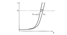
- the thermoelectric conversion rate of the diode 51 is expressed by dV / dT, and the voltage change dV is generated by the temperature rise ⁇ T of the cell unit 20. Therefore, in the steady state, from the cell unit 20 A voltage signal expressed as follows is output. The voltage-current characteristics of this diode are shown in FIG.
- the forward current of the diode 51 is obtained by using the forward voltage Vf. It is expressed.
- A is the pn junction area
- Is is the saturation current
- q is the elementary charge
- k is the Boltzmann constant
- T is the absolute temperature. From equation (10), Is obtained.
- this embodiment can also determine the position of the subject simply and at high speed. Further, even if the background temperature or the chip temperature changes, the output signal is not affected by the output of the difference between the two pixels.
- thermoelectric conversion element using a diode is easy to manufacture using a general silicon process and has a large output voltage for infrared rays.
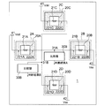
- FIG. 7 is a plan view of the solid-state imaging device 1 of the present embodiment.
- the pixels 2A to 2D are arranged at positions on the top, bottom, left, and right when viewed from the infrared incident direction (front of the paper in FIG. 7).
- the part constituted by the pixels 2A, 2B and the comparator 30A outputs the determination result A
- the part constituted by the pixels 2C, 2D and the comparator 30B outputs the determination result B.
- the determination result A is low level when the pixel 2A is irradiated with infrared rays, and is high level when the pixel 2B is irradiated with infrared rays.
- the determination result B is low level when the pixel 2C is irradiated with infrared rays, and the pixel 2D. It becomes high level when infrared rays are hit.
- the solid-state imaging device 1 according to the present embodiment outputs two pieces of information of the determination results A and B.
- the present embodiment it is possible to easily and quickly obtain information about whether the subject is present on the left or right as viewed from the solid-state image sensor and whether it is present on the top or bottom.
- the pixel arrangement method and the number of pixels are not limited to those in the present embodiment.
Landscapes
- Engineering & Computer Science (AREA)
- Multimedia (AREA)
- Signal Processing (AREA)
- Physics & Mathematics (AREA)
- Life Sciences & Earth Sciences (AREA)
- General Life Sciences & Earth Sciences (AREA)
- General Physics & Mathematics (AREA)
- Geophysics (AREA)
- Photometry And Measurement Of Optical Pulse Characteristics (AREA)
- Solid State Image Pick-Up Elements (AREA)
- Transforming Light Signals Into Electric Signals (AREA)
- Geophysics And Detection Of Objects (AREA)
Abstract
[課題]被写体の位置を高速かつ簡便に判別することを可能にする。 [解決手段]半導体基板100上に形成された少なくとも2個の赤外線検出部2A、2Bと、少なくとも2個の赤外線検出部を直列に接続する電気配線2313A、2312Bと、赤外線検出部を直列に接続する電気配線の中間の電位を、予め設定された参照電位と比較する比較部30と、を備えている。
Description
本発明は、赤外線帯に対する非冷却型(熱型)の固体撮像素子に関する。
主に8μm~12μm帯の赤外線に対応する赤外線センサは、特に室温近傍の物体から放射される赤外線に感度が高いことから、セキュリティカメラ、車載前方監視カメラに用いられている。近年、MEMS(Micro-Electro-Mechanical System)プロセスの発展に伴って、素子を冷却することなく赤外線を感知する非冷却型(熱型)の赤外線センサが主流となりつつある。
熱型の赤外線センサは、遠赤外線用のレンズ(主にGeレンズ)によって集光された赤外線を、半導体基板上にアレイ化されて上記半導体基板から熱的に隔離された画素によって吸収し、生じた画素の熱上昇を熱電変換して電気信号として読み出し、イメージ化する構成を有している。配線層の簡略化によってセルの熱容量を下げ、高速な応答が可能な熱型赤外線センサが提案されている(例えば、特許文献1参照)。
特許文献1に記載の熱型赤外線センサにおいては、配線層の簡略化によってセルの熱容量を下げ、高速な応答を可能にしている。しかし、この特許文献1に記載の熱型赤外線センサでは、被写体の位置を高速かつ簡便に判別することはできない。また、この特許文献1に記載の熱型赤外線センサは、イメージセンサであるため、1行ずつ順番に選択動作して出力信号を読み出すスキャン動作を行う必要があり、このスキャン動作には行数分の時間を要する。したがって、画素の赤外線応答速度を十分に生かすことができない。
本発明は、上記事情を考慮してなされたものであって、被写体の位置を高速かつ簡便に判別することのできる固体撮像素子を提供すことを目的とする。
本発明の一態様による固体撮像素子は、半導体基板上に形成された少なくとも2個の赤外線検出部と、少なくとも2個の前記赤外線検出部を直列に接続する電気配線と、前記赤外線検出部を直列に接続する電気配線の中間の電位を、予め設定された参照電位と比較する比較部と、を備えていることを特徴とする。
本発明によれば、被写体の位置を高速かつ簡便に判別することができる。
(第1実施形態)
本発明の第1実施形態による固体撮像素子を図1乃至図2を参照して説明する。本実施形態の固体撮像素子の平面図を図1に示し、図1に示す切断線A-Aで切断した断面を図2に示す。本実施形態の固体撮像素子1は、2個の画素(赤外線検出部)2A、2Bと、比較器30と、を備えている。各画素2A、2Bは、図2に示すようにセル部20を有している。このセル部20は、半導体基板、例えばシリコン基板100の表面部分に形成された凹部(空洞部)14の上方に配置され、支持構造部221、222によって支持される。そして、セル部20は、熱電変換素子21と、この熱電変換素子21を覆う赤外線吸収層24とを備えている。この熱電変換素子21は、赤外線吸収層24と電気的に絶縁されるとともに、支持構造部221、222内に設けられた接続配線2212、2221に電気的に接続される。これらの接続配線2212、2221は、絶縁膜(保護膜)2212、2222によってそれぞれ覆われている。そして、接続配線2212、2221は、半導体基板100上に設けられた配線2312、2313にそれぞれ接続される。この配線2312,2313は、それぞれ絶縁膜2311、2322によって覆われている。例えば、画素2Aの場合は、図1に示すように、熱電変換素子21Aは、支持構造部221、222に設けられた接続配線221A、222Aに接続されている。そして、接続配線221Aは半導体基板100上に設けられた配線2312Aを介してVdd電源41に接続され、接続配線222Aは半導体基板100上に設けられた配線2313A、ノード31を介して比較器30に接続される。また、画素2Bの場合は、図1に示すように、熱電変換素子21Bは、支持構造部221、222に設けられた接続配線221B、222Bに接続されている。そして、接続配線221Bは半導体基板100上に設けられた配線2312B、ノード31を介して比較器30に接続され、接続配線222Bは半導体基板100上に設けられた配線2313Bを介してVss電源42に接続される。比較器30は、半導体基板(半導体チップ)100上に形成されていても良いし、半導体チップ外に形成してもよい。
本発明の第1実施形態による固体撮像素子を図1乃至図2を参照して説明する。本実施形態の固体撮像素子の平面図を図1に示し、図1に示す切断線A-Aで切断した断面を図2に示す。本実施形態の固体撮像素子1は、2個の画素(赤外線検出部)2A、2Bと、比較器30と、を備えている。各画素2A、2Bは、図2に示すようにセル部20を有している。このセル部20は、半導体基板、例えばシリコン基板100の表面部分に形成された凹部(空洞部)14の上方に配置され、支持構造部221、222によって支持される。そして、セル部20は、熱電変換素子21と、この熱電変換素子21を覆う赤外線吸収層24とを備えている。この熱電変換素子21は、赤外線吸収層24と電気的に絶縁されるとともに、支持構造部221、222内に設けられた接続配線2212、2221に電気的に接続される。これらの接続配線2212、2221は、絶縁膜(保護膜)2212、2222によってそれぞれ覆われている。そして、接続配線2212、2221は、半導体基板100上に設けられた配線2312、2313にそれぞれ接続される。この配線2312,2313は、それぞれ絶縁膜2311、2322によって覆われている。例えば、画素2Aの場合は、図1に示すように、熱電変換素子21Aは、支持構造部221、222に設けられた接続配線221A、222Aに接続されている。そして、接続配線221Aは半導体基板100上に設けられた配線2312Aを介してVdd電源41に接続され、接続配線222Aは半導体基板100上に設けられた配線2313A、ノード31を介して比較器30に接続される。また、画素2Bの場合は、図1に示すように、熱電変換素子21Bは、支持構造部221、222に設けられた接続配線221B、222Bに接続されている。そして、接続配線221Bは半導体基板100上に設けられた配線2312B、ノード31を介して比較器30に接続され、接続配線222Bは半導体基板100上に設けられた配線2313Bを介してVss電源42に接続される。比較器30は、半導体基板(半導体チップ)100上に形成されていても良いし、半導体チップ外に形成してもよい。
このように構成された本実施形態の固体撮像素子において、被写体からの赤外線が入射すると、この赤外線はセル部20の赤外線吸収層24によって吸収され、生じた熱エネルギーにより、赤外線吸収層24の温度が上昇する。この温度の変化が熱電変換素子21によって電気信号に変換されて画素の出力となる。そして、画素2Aと、画素2Bの出力を比較器30において、比較することによって、被写体の位置を検出する。
本実施形態の固体撮像素子は、真空中で動作させるため、セル部20からの熱の逃げ道は支持構造部221、222のみとなる。したがって、セル部20の熱隔離性は、支持構造部221、222の熱コンダクタンスによって決定され、支持構造部の長さを長く構成すればするほど、また細く構成すればするほど断熱性は向上する。
支持構造全体の熱コンダクタンスをGthとすると、赤外線吸収層24において生じた熱エネルギーによってセル部20の温度変化ΔTは、

にしたがって上昇していく。ここでPaはセル部20に入射した赤外線エネルギー(W)、Cthはセルの熱容量(J/K)、tは受信開始後の経過時間(s)である。
そして、セル部20の温度は熱時定数τで定常状態になる。この熱時定数は、

により計算される。
セル部20は、一辺が30μm程度の四角形でかつ高さが4μm~5μm程度とし、またセル部20を支持する支持構造部が2本で構成され、各支持構造部の保護膜の断面を一辺が1μm程度の四角形とし、セル部20から接続配線の保護膜にいたる長さを70μm程度としたとき、上記熱時定数はおおよそ20msec~50msec程度のオーダーとなる。赤外線の受光によるセルの温度上昇分は、

となる。
ここで、セル部20の温度上昇ΔTを検出するために、熱電変換素子21として、本実施形態においては、抵抗体を用いる。抵抗体21の温度に対する抵抗変化の性質を用いて、セル部20の温度上昇を電気信号として取り出すことができる。
抵抗体21の、温度変化に応じた抵抗変化(温度抵抗係数)をdR/dTとする。これは例えば抵抗体21として、抵抗値100kΩがTiN(窒化チタン)を用いた場合、温度1℃の変化に対して150Ωの抵抗変化となる。
ここで、画素2A、2Bは、図1に示すように半導体基板100上の2箇所にそれぞれ形成されている。被写体の位置に応じて、これらの画素2A、2Bのいずれかに赤外線が照射される。被写体からの赤外線が画素2Aにのみ照射されている場合、そのときの画素2Aのみに式(3)で表される温度変化が生じる。
画素2A及び画素2Bは配線によって接続されており、Vdd電源41及びVss電源42によって、画素2A及び画素2Bには直列に電圧が印加される。このとき抵抗体21Aの抵抗値をR+ΔR、抵抗体21Bの抵抗値をRとすると、画素2A及び画素2Bには、

で表される電流が流れる。したがって、接続配線2313Aと接続配線2312Bが接続されるノード31の電位V31は、

となる。
比較器30は、ノードの電位V31を、次式(6)で表される閾値電圧Vth

と比較する。上述したように、画素2Aに赤外線が照射している場合は、

と、ノードの電位V31は閾値電圧Vthよりも低くなるが、逆に画素2Bに赤外線が照射している場合は、

となり、上述した場合と逆となる。
例えば、R=1MΩ、ΔR=1kΩ、Vdd=5V、Vss=-5Vとすると、V31-Vth=2.5mV程度となる。
比較器30の一具体例を図3に示す。この具体例の比較器30は、入力端子がオペアンプ301の入力302に相当する。抵抗303及び抵抗304を直列に接続し、抵抗303の一端を接地し、抵抗304の一端をオペアンプ301の出力端子に接続し、抵抗303及び抵抗304の共通接続ノードをオペアンプ301の反転入力端子に接続する。このような構成とすることにより、オペアンプ301は、非反転増幅回路を形成している。増幅率は1+R2/R1で表されるため、たとえばR2=1MΩ、R1=1kΩとすると増幅率は約1000倍となる。
非反転増幅回路301の出力はコンパレータ307に入力される。コンパレータ307のもう一方の入力端子306の電位は比較対象となる閾値電圧Vthに固定されている。V31-Vthが非常に小さい場合にコンパレータ307の出力が変化しないように、すなわち不感領域を持たせるために、コンパレータ307の2入力端子にはダイオード309A及びダイオード309Bが接続され、2端子の電位差がいずれかのダイオードに電流を流すに足る程度、例えば0.6V程度となったときにコンパレータ307が電位差を認識することになる。コンパレータ307の出力は、V31-Vthの符号にしたがって、ハイレベルかロウレベルのいずれかとなる。
このように、比較器30は閾値電圧Vthとノード31の電位V31を比較することによって、平面的に離れた画素2Aと画素2Bのどちらかに赤外線信号が当たっているかを簡便に判別することができる。
本実施形態によれば、簡便かつ高速に、被写体の位置を判別することができる。さらに、背景温度やチップ温度が変化したとしても、2画素の差分を出力しているために出力信号はそれらの影響を受けない。
(第2実施形態)
次に、本発明の第2実施形態による固体撮像素子を図4および図5を参照して説明する。本実施形態の固体撮像素子1の平面図を図4に示し、図4に示す切断線A-Aで切断した断面を図5に示す。本実施形態の固体撮像素子1は、第1実施形態の固体撮像素子1において、抵抗体からなる熱電変換素子21をpn接合のダイオード51に置き換えた構成となっている。すなわち、画素2Aには熱電変換素子としてダイオード51Aが用いられ、画素2Bには熱電変換素子としてダイオード51Bが用いられる。
次に、本発明の第2実施形態による固体撮像素子を図4および図5を参照して説明する。本実施形態の固体撮像素子1の平面図を図4に示し、図4に示す切断線A-Aで切断した断面を図5に示す。本実施形態の固体撮像素子1は、第1実施形態の固体撮像素子1において、抵抗体からなる熱電変換素子21をpn接合のダイオード51に置き換えた構成となっている。すなわち、画素2Aには熱電変換素子としてダイオード51Aが用いられ、画素2Bには熱電変換素子としてダイオード51Bが用いられる。
このダイオード51は、セル部20の下部に形成されたp型半導体層211と、n型半導体層212と、を有している。p型半導体層211は、プラグ252を介して、配線251に接続され、この配線251は接続配線2211に接続される。また、n型半導体層212は、プラグ254を介して、配線253に接続され、この配線253は接続配線2221に接続される。
本実施形態においては、セルの温度上昇ΔTは、セル部20の下層に構成されたダイオードの51によって検出される。ダイオード51の熱電変換率はdV/dTで表され、セル部20の温度上昇ΔTによって電圧変化dVが発生する。したがって定常状態では、セル部20から

であらわされる電圧信号が出力される。このダイオードの電圧-電流特性を図6に示す。
ダイオード51の順方向電流は、順方向電圧Vfを用いて

と表される。ここで、Aはpn接合面積、Isは飽和電流、qは電荷素量、kはボルツマン定数、Tは絶対温度である。式(10)より、

が得られる。セル部20の温度が上昇すると、順方向電圧Vfは低くなるため、ダイオード51の抵抗値が下がることになる。この変化分をΔRとすると、ΔR<0となり、第1実施形態とは符号が逆になる。例えば、画素2Aに赤外線が当たっている場合は、ノード31の電位V31と、閾値電圧Vthとの差(=V31-Vth)は、

となる。
逆に、画素2Bに赤外線が当たっている場合は、上記差は負となり、画素2Aと画素2Bどちらに赤外線が当たっているのか、判別が可能である。
本実施形態も第1実施形態と同様に、簡便かつ高速に、被写体の位置を判別することができる。さらに、背景温度やチップ温度が変化したとしても、2画素の差分を出力しているために出力信号はそれらの影響を受けない。
また、本実施形態のように、ダイオードを用いた熱電変換素子は、シリコンの汎用プロセスを用いて製造が簡単であり、かつ赤外線に対する出力電圧が大きい。
(第3実施形態)
次に、本発明の第3実施形態による固体撮像素子を図7に示す。図7は、本実施形態の固体撮像素子1の平面図である。本実施形態の固体撮像素子1は、図7に示すように、画素2A~2Dを、赤外線入射方向(図7においては、紙面の手前)から見て、上下左右の位置に配置する。画素2A、2B及び比較器30Aにて構成される部分は判断結果Aを出力し、画素2C、2D及び比較器30Bにて構成される部分は判断結果Bを出力する。判断結果Aは、画素2Aに赤外線が当たっているときにロウレベル、画素2Bに赤外線が当たっているときにハイレベルとなり、判断結果Bは、画素2Cに赤外線が当たっているときにロウレベル、画素2Dに赤外線が当たっているときにハイレベルとなる。本実施形態による固体撮像素子1は、判断結果AとBという2つの情報を出力することになる。
次に、本発明の第3実施形態による固体撮像素子を図7に示す。図7は、本実施形態の固体撮像素子1の平面図である。本実施形態の固体撮像素子1は、図7に示すように、画素2A~2Dを、赤外線入射方向(図7においては、紙面の手前)から見て、上下左右の位置に配置する。画素2A、2B及び比較器30Aにて構成される部分は判断結果Aを出力し、画素2C、2D及び比較器30Bにて構成される部分は判断結果Bを出力する。判断結果Aは、画素2Aに赤外線が当たっているときにロウレベル、画素2Bに赤外線が当たっているときにハイレベルとなり、判断結果Bは、画素2Cに赤外線が当たっているときにロウレベル、画素2Dに赤外線が当たっているときにハイレベルとなる。本実施形態による固体撮像素子1は、判断結果AとBという2つの情報を出力することになる。
判断結果AとBの結果の組み合わせにより、被写体が(左または上)(左または下)(右または上)(右または下)のいずれに存在するかを知ることができる。
本実施形態により、固体撮像素子からみて被写体が左右いずれに存在するか、に加え、上下いずれに存在するか、の情報を、簡便かつ高速に得ることができる。なお、画素の配置方法や画素数は本実施形態に限らない。
1 固体撮像素子
2、2A、2B 画素(赤外線検出部)
20 セル部
21、21A、21B、21C、21D 熱電変換素子
24 赤外線吸収層
30 比較器
221 支持構造部
221A 接続配線
221B 接続配線
222 支持構造部
222A 接続配線
222B 接続配線
2312A 配線
2312B 配線
2313A 配線
2313B 配線
2、2A、2B 画素(赤外線検出部)
20 セル部
21、21A、21B、21C、21D 熱電変換素子
24 赤外線吸収層
30 比較器
221 支持構造部
221A 接続配線
221B 接続配線
222 支持構造部
222A 接続配線
222B 接続配線
2312A 配線
2312B 配線
2313A 配線
2313B 配線
Claims (7)
- 半導体基板上に形成された少なくとも2個の赤外線検出部と、
少なくとも2個の前記赤外線検出部を直列に接続する電気配線と、
前記赤外線検出部を直列に接続する電気配線の中間の電位を、予め設定された参照電位と比較する比較部と、
を備えていることを特徴とする固体撮像素子。 - 前記複数の赤外線検出部はそれぞれ、
前記半導体上に形成された第1および第2配線部と、
前記半導体基板の表面部分に形成された凹部の上方に配置され、前記第1および第2配線部とそれぞれ電気的に接続される第1および第2接続配線を有する第1および第2支持構造部と、
前記凹部の上方に配置され、前記第1および第2支持構造部によって支持されるセル部と、
を備え、前記セル部は、
入射された赤外線を吸収する赤外線吸収層と、
前記第1および第2支持構造部と電気的に接続されると共に、前記赤外線吸収層と電気的に絶縁され、前記セル部の温度変化を検出することにより、電気信号を生成する複数の熱電変換素子と、
を有していることを特徴とする請求項1記載の固体撮像素子。 - 前記熱電変換素子は、抵抗体であることを特徴とする請求項1記載の固体撮像素子。
- 前記熱電変換素子は、pn接合ダイオードであることを特徴とする請求項1記載の固体撮像素子。
- 前記比較部は、
前記電気配線の中間の電位が入力される正入力端子と、出力が、直列に接続された少なくとも2個の抵抗によって分圧された分圧電圧が入力される反転入力端子を有する非反転増幅回路と、
前記非反転増幅回路の出力と、前記参照電位を比較するコンパレータと、
を備えていることを特徴とする請求項1記載の固体撮像素子。 - 前記赤外線検出部は4個であって、2個の赤外線検出部と、残りの2個の赤外線検出部は、互いに直交する方向に配置され、前記2個の赤外線検出部を電気的に接続する第1電気配線と、前記残りの2個の赤外線検出部を電気的に接続する第2電気配線とをさらに備えていることを特徴とする請求項1記載の固体撮像素子。
- 前記比較部は、前記第1電気配線の中間の電位を第1の参照電位と比較する第1比較回路と、前記第2電気配線の中間の電位を第2の参照電位と比較する第2比較回路と、を備えていることを特徴とする請求項6記載の固体撮像素子。
Priority Applications (1)
| Application Number | Priority Date | Filing Date | Title |
|---|---|---|---|
| US13/052,903 US8212214B2 (en) | 2008-09-25 | 2011-03-21 | Solid-state imaging element |
Applications Claiming Priority (2)
| Application Number | Priority Date | Filing Date | Title |
|---|---|---|---|
| JP2008246300A JP5543703B2 (ja) | 2008-09-25 | 2008-09-25 | 被写体位置検出素子 |
| JP2008-246300 | 2008-09-25 |
Related Child Applications (1)
| Application Number | Title | Priority Date | Filing Date |
|---|---|---|---|
| US13/052,903 Continuation US8212214B2 (en) | 2008-09-25 | 2011-03-21 | Solid-state imaging element |
Publications (1)
| Publication Number | Publication Date |
|---|---|
| WO2010035624A1 true WO2010035624A1 (ja) | 2010-04-01 |
Family
ID=42059630
Family Applications (1)
| Application Number | Title | Priority Date | Filing Date |
|---|---|---|---|
| PCT/JP2009/065493 Ceased WO2010035624A1 (ja) | 2008-09-25 | 2009-09-04 | 固体撮像素子 |
Country Status (3)
| Country | Link |
|---|---|
| US (1) | US8212214B2 (ja) |
| JP (1) | JP5543703B2 (ja) |
| WO (1) | WO2010035624A1 (ja) |
Families Citing this family (3)
| Publication number | Priority date | Publication date | Assignee | Title |
|---|---|---|---|---|
| CN104639234B (zh) * | 2013-11-07 | 2018-01-19 | 珠海格力电器股份有限公司 | 评估红外光干扰强度的方法及装置 |
| US10454493B2 (en) * | 2016-05-10 | 2019-10-22 | Analog Devices Global | Integrated circuit with on chip variation reduction |
| KR102355553B1 (ko) * | 2016-09-02 | 2022-01-26 | 소니 세미컨덕터 솔루션즈 가부시키가이샤 | 촬상 장치 |
Citations (10)
| Publication number | Priority date | Publication date | Assignee | Title |
|---|---|---|---|---|
| JPH06323905A (ja) * | 1993-05-11 | 1994-11-25 | Opt Kk | 受動型赤外線検知装置 |
| JPH08201166A (ja) * | 1995-01-30 | 1996-08-09 | Murata Mfg Co Ltd | 赤外線センサ |
| JPH09292277A (ja) * | 1996-04-26 | 1997-11-11 | Matsushita Electric Works Ltd | 赤外線検出装置 |
| WO1997046896A1 (en) * | 1996-06-07 | 1997-12-11 | Nihon Shingo Kabushiki Kaisha | Variable-axis photodetector |
| JPH1151764A (ja) * | 1997-07-31 | 1999-02-26 | Opt Kk | 受動型赤外線検知装置 |
| JPH11230605A (ja) * | 1998-02-13 | 1999-08-27 | Mitsubishi Electric Corp | 空気調和機 |
| JP2000111397A (ja) * | 1998-10-05 | 2000-04-18 | Nec Corp | 二次元アレイ型赤外線検出素子とその製造方法 |
| JP2001318166A (ja) * | 2000-05-09 | 2001-11-16 | Matsuda Micronics Corp | 防犯用サーモパイル放射遠赤外線検出装置 |
| JP2004117277A (ja) * | 2002-09-27 | 2004-04-15 | Toshiba Corp | 赤外線撮像装置 |
| JP2005188970A (ja) * | 2003-12-24 | 2005-07-14 | Matsushita Electric Ind Co Ltd | 熱型赤外線固体撮像装置および赤外線カメラ |
Family Cites Families (14)
| Publication number | Priority date | Publication date | Assignee | Title |
|---|---|---|---|---|
| US4032777A (en) * | 1976-03-29 | 1977-06-28 | Mccaleb Robert Earl | Photomeric monitoring device |
| US4645919A (en) * | 1985-02-04 | 1987-02-24 | Mccaleb Robert E | Photosensitive motion detector apparatus |
| JP3013269B2 (ja) * | 1991-08-15 | 2000-02-28 | 松下電工株式会社 | 赤外線検知回路 |
| EP0624857B1 (en) * | 1993-05-11 | 1998-09-09 | Optex Co. Ltd. | Passive type moving object detection system |
| JPH07128140A (ja) * | 1993-10-29 | 1995-05-19 | Matsushita Electric Works Ltd | 赤外線検出素子 |
| JP3327668B2 (ja) * | 1994-03-24 | 2002-09-24 | 石塚電子株式会社 | 赤外線検出器 |
| US5486698A (en) * | 1994-04-19 | 1996-01-23 | Texas Instruments Incorporated | Thermal imaging system with integrated thermal chopper |
| US6367972B1 (en) * | 1998-09-29 | 2002-04-09 | Ishizuka Electronics Corporation | Non-contact temperature sensor with temperature compensating heat sensitive elements on plastic film |
| JP3946406B2 (ja) * | 2000-03-30 | 2007-07-18 | 株式会社東芝 | 熱型赤外線センサの製造方法 |
| JP3589997B2 (ja) * | 2001-03-30 | 2004-11-17 | 株式会社東芝 | 赤外線センサおよびその製造方法 |
| JP3959480B2 (ja) | 2001-06-15 | 2007-08-15 | 三菱電機株式会社 | 赤外線検出器 |
| JP3616622B2 (ja) * | 2002-08-26 | 2005-02-02 | 株式会社東芝 | 赤外線撮像装置 |
| JP2006349625A (ja) * | 2005-06-20 | 2006-12-28 | Mitsubishi Electric Corp | 紫外線量測定装置および携帯電話機および紫外線量測定方法 |
| JP2009074855A (ja) * | 2007-09-19 | 2009-04-09 | Oki Semiconductor Co Ltd | 光検出装置 |
-
2008
- 2008-09-25 JP JP2008246300A patent/JP5543703B2/ja active Active
-
2009
- 2009-09-04 WO PCT/JP2009/065493 patent/WO2010035624A1/ja not_active Ceased
-
2011
- 2011-03-21 US US13/052,903 patent/US8212214B2/en active Active
Patent Citations (10)
| Publication number | Priority date | Publication date | Assignee | Title |
|---|---|---|---|---|
| JPH06323905A (ja) * | 1993-05-11 | 1994-11-25 | Opt Kk | 受動型赤外線検知装置 |
| JPH08201166A (ja) * | 1995-01-30 | 1996-08-09 | Murata Mfg Co Ltd | 赤外線センサ |
| JPH09292277A (ja) * | 1996-04-26 | 1997-11-11 | Matsushita Electric Works Ltd | 赤外線検出装置 |
| WO1997046896A1 (en) * | 1996-06-07 | 1997-12-11 | Nihon Shingo Kabushiki Kaisha | Variable-axis photodetector |
| JPH1151764A (ja) * | 1997-07-31 | 1999-02-26 | Opt Kk | 受動型赤外線検知装置 |
| JPH11230605A (ja) * | 1998-02-13 | 1999-08-27 | Mitsubishi Electric Corp | 空気調和機 |
| JP2000111397A (ja) * | 1998-10-05 | 2000-04-18 | Nec Corp | 二次元アレイ型赤外線検出素子とその製造方法 |
| JP2001318166A (ja) * | 2000-05-09 | 2001-11-16 | Matsuda Micronics Corp | 防犯用サーモパイル放射遠赤外線検出装置 |
| JP2004117277A (ja) * | 2002-09-27 | 2004-04-15 | Toshiba Corp | 赤外線撮像装置 |
| JP2005188970A (ja) * | 2003-12-24 | 2005-07-14 | Matsushita Electric Ind Co Ltd | 熱型赤外線固体撮像装置および赤外線カメラ |
Also Published As
| Publication number | Publication date |
|---|---|
| US20110226953A1 (en) | 2011-09-22 |
| JP2010078423A (ja) | 2010-04-08 |
| JP5543703B2 (ja) | 2014-07-09 |
| US8212214B2 (en) | 2012-07-03 |
Similar Documents
| Publication | Publication Date | Title |
|---|---|---|
| JP4975669B2 (ja) | 赤外線検出器およびこの赤外線検出器を備えた固体撮像素子 | |
| JP4677044B2 (ja) | 非冷却lwir検出器に組み合わされた可視すなわちswir検出器を有するデュアル・バンド撮像装置 | |
| JP5443793B2 (ja) | 赤外線固体撮像素子 | |
| US7489024B2 (en) | TMOS-infrared uncooled sensor and focal plane array | |
| JP5455844B2 (ja) | 非冷却赤外線イメージセンサ | |
| KR100928200B1 (ko) | 바이폴라 트랜지스터 기반의 비냉각형 적외선 센서 및 그의제조 방법 | |
| US7095027B1 (en) | Multispectral multipolarization antenna-coupled infrared focal plane array | |
| US9170160B2 (en) | Imaging device | |
| US20220214223A1 (en) | Combined near and mid infrared sensor in a chip scale package | |
| JP5425127B2 (ja) | 固体撮像素子 | |
| JP5543703B2 (ja) | 被写体位置検出素子 | |
| JP6026585B2 (ja) | 赤外線撮像装置 | |
| KR101677717B1 (ko) | 멤스 써모파일 센서 및 그 제조방법 | |
| JP2005188970A (ja) | 熱型赤外線固体撮像装置および赤外線カメラ | |
| JP2006177712A (ja) | 半導体装置及びその製造方法 | |
| JP2000230857A (ja) | 熱型赤外線センサおよび熱型赤外線アレイ素子 | |
| JP5443800B2 (ja) | 赤外線固体撮像素子 | |
| JP3441405B2 (ja) | 半導体赤外線検出素子 | |
| US7485860B2 (en) | Thermoelectric bridge IR detector | |
| JP5629146B2 (ja) | 温度センサ | |
| JP5738954B2 (ja) | 固体撮像素子 | |
| US9068882B2 (en) | Low power thermal imager | |
| WO2011121706A1 (ja) | 赤外線撮像素子および赤外線撮像装置 | |
| CN114353957A (zh) | 一种二极管型非制冷红外探测器 | |
| JP2012013516A (ja) | 赤外線センサ装置 |
Legal Events
| Date | Code | Title | Description |
|---|---|---|---|
| 121 | Ep: the epo has been informed by wipo that ep was designated in this application |
Ref document number: 09816041 Country of ref document: EP Kind code of ref document: A1 |
|
| NENP | Non-entry into the national phase |
Ref country code: DE |
|
| 122 | Ep: pct application non-entry in european phase |
Ref document number: 09816041 Country of ref document: EP Kind code of ref document: A1 |