WO2010001623A1 - 青色蛍光体およびそれを用いた発光装置 - Google Patents
青色蛍光体およびそれを用いた発光装置 Download PDFInfo
- Publication number
- WO2010001623A1 WO2010001623A1 PCT/JP2009/003103 JP2009003103W WO2010001623A1 WO 2010001623 A1 WO2010001623 A1 WO 2010001623A1 JP 2009003103 W JP2009003103 W JP 2009003103W WO 2010001623 A1 WO2010001623 A1 WO 2010001623A1
- Authority
- WO
- WIPO (PCT)
- Prior art keywords
- blue phosphor
- emitting device
- phosphor
- firing
- ray
- Prior art date
Links
Images

Classifications
-
- H—ELECTRICITY
- H01—ELECTRIC ELEMENTS
- H01J—ELECTRIC DISCHARGE TUBES OR DISCHARGE LAMPS
- H01J11/00—Gas-filled discharge tubes with alternating current induction of the discharge, e.g. alternating current plasma display panels [AC-PDP]; Gas-filled discharge tubes without any main electrode inside the vessel; Gas-filled discharge tubes with at least one main electrode outside the vessel
- H01J11/10—AC-PDPs with at least one main electrode being out of contact with the plasma
- H01J11/12—AC-PDPs with at least one main electrode being out of contact with the plasma with main electrodes provided on both sides of the discharge space
-
- C—CHEMISTRY; METALLURGY
- C09—DYES; PAINTS; POLISHES; NATURAL RESINS; ADHESIVES; COMPOSITIONS NOT OTHERWISE PROVIDED FOR; APPLICATIONS OF MATERIALS NOT OTHERWISE PROVIDED FOR
- C09K—MATERIALS FOR MISCELLANEOUS APPLICATIONS, NOT PROVIDED FOR ELSEWHERE
- C09K11/00—Luminescent, e.g. electroluminescent, chemiluminescent materials
- C09K11/08—Luminescent, e.g. electroluminescent, chemiluminescent materials containing inorganic luminescent materials
- C09K11/77—Luminescent, e.g. electroluminescent, chemiluminescent materials containing inorganic luminescent materials containing rare earth metals
- C09K11/7728—Luminescent, e.g. electroluminescent, chemiluminescent materials containing inorganic luminescent materials containing rare earth metals containing europium
- C09K11/7736—Vanadates; Chromates; Molybdates; Tungstates
-
- H—ELECTRICITY
- H01—ELECTRIC ELEMENTS
- H01J—ELECTRIC DISCHARGE TUBES OR DISCHARGE LAMPS
- H01J11/00—Gas-filled discharge tubes with alternating current induction of the discharge, e.g. alternating current plasma display panels [AC-PDP]; Gas-filled discharge tubes without any main electrode inside the vessel; Gas-filled discharge tubes with at least one main electrode outside the vessel
- H01J11/20—Constructional details
- H01J11/34—Vessels, containers or parts thereof, e.g. substrates
- H01J11/42—Fluorescent layers
-
- H—ELECTRICITY
- H01—ELECTRIC ELEMENTS
- H01J—ELECTRIC DISCHARGE TUBES OR DISCHARGE LAMPS
- H01J61/00—Gas-discharge or vapour-discharge lamps
- H01J61/02—Details
- H01J61/38—Devices for influencing the colour or wavelength of the light
- H01J61/42—Devices for influencing the colour or wavelength of the light by transforming the wavelength of the light by luminescence
- H01J61/44—Devices characterised by the luminescent material
Definitions
- the present invention relates to a blue phosphor used for a plasma display panel (hereinafter referred to as PDP), a mercury-free fluorescent lamp, and the like, and a light emitting device (particularly a PDP) using the blue phosphor.
- PDP plasma display panel
- a mercury-free fluorescent lamp and the like
- a light emitting device particularly a PDP
- BAM Eu, which has high brightness by vacuum ultraviolet light excitation, has been used as a blue phosphor for PDP.
- the luminance degradation mechanism of the blue phosphor BAM: Eu has not been fully elucidated, it is not possible to remove the phosphor due to the mixing and heat treatment of moisture and impurity gas in the light emitting device manufacturing process and the vacuum ultraviolet light irradiation when the light emitting device is driven. It is considered that the luminance deteriorates.
- Patent Document 1 a method of adding gadolinium to the phosphor (see, for example, Patent Document 1), a method of coating the phosphor with a divalent metal silicate such as an alkaline earth metal (for example, Patent Document) 2), and a method of coating the phosphor with antimony oxide (for example, see Patent Document 3).
- Patent Documents 4 and 5 phosphors having improved luminance of blue light emitting components and high luminance by vacuum ultraviolet light excitation have been proposed (see Patent Documents 4 and 5).
- An object of the present invention is to solve the above-described conventional problems, and to provide a blue phosphor having high luminance and less luminance deterioration when the light emitting device is driven. It is another object of the present invention to provide a long-life light emitting device using the blue phosphor, particularly a PDP.
- the blue phosphor of the present invention has a general formula of aBaO.bSrO. (1-ab) EuO.cMgO.dAlO 3 / 2.eWO 3 (0.70 ⁇ a ⁇ 0.95). 0 ⁇ b ⁇ 0.15, 0.95 ⁇ c ⁇ 1.15, 9.00 ⁇ d ⁇ 11.00, 0.001 ⁇ e ⁇ 0.200, where a + b ⁇ 0.97) It consists of a metal aluminate and ZrO 2, and contains ZrO 2 in a proportion of 0.01 to 1.00% by weight. In the X-ray diffraction pattern measured with X-rays with a wavelength of 0.774 mm, the peak top is There are two peaks with a diffraction angle 2 ⁇ in the range of 13.0 to 13.6 degrees.
- the present invention also provides a light emitting device comprising a phosphor layer containing the blue phosphor of the present invention.
- the present invention it is possible to provide a blue phosphor that has high luminance and little luminance deterioration when the light emitting device is manufactured and driven.
- a light emitting device such as a long-life PDP in which luminance does not deteriorate even when driven for a long time.
- the blue phosphor of the present invention has a general formula aBaO.bSrO. (1-ab) EuO.cMgO.dAlO 3 / 2.eWO 3 (0.70 ⁇ a ⁇ 0.95, 0 ⁇ b ⁇ 0.15). 0.95 ⁇ c ⁇ 1.15, 9.00 ⁇ d ⁇ 11.00, 0.001 ⁇ e ⁇ 0.200, provided that a + b ⁇ 0.97) and ZrO 2 And ZrO 2 is contained at a ratio of 0.01 to 1.00% by weight.
- the blue phosphor of the present invention preferably contains ZrO 2 in a proportion of 0.01 to 0.10% by weight.
- the blue phosphor of the present invention has two peaks with a peak top in the range of 13.0 to 13.6 degrees at a diffraction angle 2 ⁇ in an X-ray diffraction pattern measured with an X-ray having a wavelength of 0.774 mm. Exists. In the X-ray diffraction pattern measured with an X-ray having a wavelength of 0.774 mm, the peak top of one of the two peaks is within a range of 13.0 to 13.2 degrees at a diffraction angle 2 ⁇ . Is preferable from the viewpoint of luminance and luminance deterioration resistance.
- the inventors of the present invention have a high luminance and have a high luminance when the light-emitting device is manufactured and when it is driven, according to the blue phosphor having the above-described composition and satisfying the characteristics related to the X-ray diffraction pattern. It has been found that a phosphor with less luminance degradation can be obtained.
- the conventional BAM Eu blue phosphor, there was one peak having a peak top within the above-mentioned diffraction angle 2 ⁇ (13.0 to 13.6 degrees).
- the reason why the blue phosphor of the present invention satisfying the above-mentioned characteristics relating to the X-ray diffraction pattern is excellent is not clear, but according to the experiments by the present inventors, firing is performed under special conditions described later.
- the blue phosphor of the present invention obtained by this the lattice constant of the phosphor changes, and this change is presumed to have improved the emission characteristics (luminance degradation resistance) of the phosphor.
- a BL19B2 powder X-ray diffraction apparatus (Debye-Scherrer optical system using an imaging plate, hereinafter referred to as BL19 diffraction apparatus) of the large synchrotron radiation facility SPring8 is used.
- a glass capillary made of Lindeman having an inner diameter of 200 ⁇ m is filled with the phosphor powder without any gaps.
- the incident X-ray wavelength is set to about 0.774 mm by a monochromator.
- the diffraction intensity is recorded on the imaging plate while rotating the sample with a goniometer. The measurement time is carefully determined so as not to cause saturation of the imaging plate. For example, 5 minutes.
- the imaging plate is developed and the X-ray diffraction spectrum is read.
- the zero point error when reading data from the developed imaging plate is about 0.03 degree at the diffraction angle 2 ⁇ .
- Rietan For Rietveld analysis, the Rietan-2000 program (Rev. 2.3.9 and later, hereinafter referred to as Rietan) is used (by Izumi Nakai and Fujio Izumi, “Practice of X-ray powder analysis-Introduction to the Rietveld method”). (See, Japan Society for Analytical Chemistry X-ray Analysis Research Roundtable, Asakura Shoten, 2002, and http://homepage.mac.com/fujioizumi/).
- the blue phosphor of the present invention can be obtained by firing in a weak reducing atmosphere and firing in a weak oxidizing atmosphere. Firing in this weakly oxidizing atmosphere is performed in the temperature lowering process during firing. Specifically, in the firing step, first, firing is performed in a weakly reducing mixed gas containing hydrogen, nitrogen and oxygen, and further, in the temperature lowering process, firing is performed in a weakly oxidizing mixed gas containing nitrogen and oxygen. It can be produced by providing (weakly oxidative mixed gas region). Below, an example of the method of manufacturing the blue fluorescent substance of this invention is demonstrated.
- Barium raw materials include high-purity (purity 99% or higher) barium hydroxide, barium carbonate, barium nitrate, barium halide, barium oxalate, or other barium compounds that can be converted to barium oxide by firing or high-purity (purity 99% or higher) ) Barium oxide.
- strontium raw material high purity (purity 99% or more) strontium hydroxide, strontium carbonate, strontium nitrate, strontium halide, strontium oxalate, or the like can be converted to strontium oxide by firing or high purity (purity 99% or more).
- Strontium oxide As the strontium raw material, high purity (purity 99% or more) strontium hydroxide, strontium carbonate, strontium nitrate, strontium halide, strontium oxalate, or the like can be converted to strontium oxide by firing or high purity (purity 99% or more).
- Europium raw materials include high-purity (99% or higher purity) europium hydroxide, europium carbonate, europium nitrate, europium halide, europium oxalate, etc. ) Europium oxide can be used.
- Magnesium raw materials such as high purity (99% or more purity) magnesium hydroxide, magnesium carbonate, magnesium nitrate, magnesium halide, magnesium oxalate, basic magnesium carbonate, etc., magnesium compounds that can be converted to magnesium oxide by firing, or high purity Magnesium oxide having a purity of 99% or more can be used.
- an aluminum compound that can be converted to alumina by firing such as high-purity (purity 99% or higher) aluminum hydroxide, aluminum nitrate, or aluminum halide, or high-purity (purity 99.9% or higher) alumina is used. Can do.
- various raw materials that can be converted into oxides by firing can be used for the tungsten raw material and the zirconium raw material.
- the blue phosphor of the present invention is produced by mixing and firing the above raw materials.
- a method of mixing the raw materials wet mixing in a solution or dry mixing of a dry powder may be used, which is industrially usual.
- a ball mill, a medium stirring mill, a planetary mill, a vibration mill, a jet mill, a V-type mixer, a stirrer, or the like can be used.
- the coarse particles in the raw material adversely affect the light emission characteristics, it is preferable to perform classification in order to make the particle sizes uniform.
- the mixed powder is fired in a mixed gas containing hydrogen, nitrogen and oxygen at 1200 to 1600 ° C. for 1 to 50 hours.
- the hydrogen concentration is 0.1 to 10% by volume
- the oxygen partial pressure is adjusted to around 1 ⁇ 10 ⁇ 7 to 1 ⁇ 10 ⁇ 2 Pa (1 ⁇ 10 ⁇ 12 to 1 ⁇ 10 ⁇ 7 atm).
- More preferable conditions are 1300 to 1400 in a weak reducing atmosphere adjusted to an oxygen partial pressure in the vicinity of 1 ⁇ 10 ⁇ 6 to 1 ⁇ 10 ⁇ 4 Pa (1 ⁇ 10 ⁇ 11 to 1 ⁇ 10 ⁇ 9 atm). Firing at 4 ° C. for 4 hours, and providing a weakly oxidative mixed gas region containing nitrogen and oxygen in the temperature lowering process.
- the oxygen partial pressure in the weakly oxidizing atmosphere only needs to be higher than the oxygen partial pressure in the weakly reducing atmosphere.
- furnace used for firing a furnace generally used in industry can be used.
- a continuous or batch type electric furnace or gas furnace such as a pusher furnace can be used.
- calcining is performed at a temperature range of 800 to 1400 ° C. before the main calcination. It is preferable. Moreover, in order to accelerate
- the obtained phosphor powder is pulverized again using a ball mill, a jet mill or the like, and further washed or classified as necessary to adjust the particle size distribution and fluidity of the phosphor powder.
- a light-emitting device with high luminance and luminance deterioration resistance can be configured.
- BAM: Eu may be replaced with the blue phosphor of the present invention, and the light emitting device may be configured according to a known method.
- the light emitting device include a PDP, a fluorescent panel, a fluorescent lamp, and the like. Among these, a PDP is preferable.
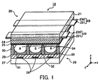
- FIG. 1 is a perspective sectional view showing the main structure of an AC surface discharge type PDP 10. Note that the PDP shown here is illustrated with a size setting in accordance with a 42-inch 1024 ⁇ 768 pixel specification for convenience, but may be applied to other sizes and specifications.
- this PDP 10 has a front panel 20 and a back panel 26, and is arranged so that the main surfaces thereof face each other.
- the front panel 20 is provided with a pair of electrodes.
- the front panel 20 includes a front panel glass 21 as a front substrate and a pair of strip-shaped display electrodes (X electrode 23 and Y electrode 22) provided on one main surface of the front panel glass 21.
- a front-side dielectric layer 24 having a thickness of about 30 ⁇ m covering the display electrode, and a protective layer 25 having a thickness of about 1.0 ⁇ m provided on the front-side dielectric layer 24.
- the display electrode includes strip-shaped transparent electrodes 220 and 230 having a thickness of 0.1 ⁇ m and a width of 150 ⁇ m, and bus lines 221 and 231 having a thickness of 7 ⁇ m and a width of 95 ⁇ m provided on the transparent electrodes 220 and 230, respectively.
- a plurality of pairs of display electrodes (X electrode 23 and Y electrode 22) are arranged in the y-axis direction with the x-axis direction as the longitudinal direction.
- Each pair of display electrodes (X electrode 23, Y electrode 22) is electrically connected to a panel drive circuit (not shown) in the vicinity of the end of the front panel glass 21 in the width direction (y-axis direction).
- the Y electrodes 22 are collectively connected to the panel drive circuit, and the X electrodes 23 are independently connected to the panel drive circuit.
- a surface discharge (sustain discharge) is generated in the gap (about 80 ⁇ m) between the X electrode 23 and the Y electrode 22.
- the X electrode 23 can also be operated as a scan electrode, and thereby, a write discharge (address discharge) can be generated between the X electrode 23 and an address electrode 28 described later.
- the back panel 26 includes a back panel glass 27 as a back substrate, a plurality of address electrodes 28, a back side dielectric layer 29, a partition wall 30, and any of red (R), green (G), and blue (B).
- Phosphor layers 31 to 33 corresponding to the above.
- the phosphor layers 31 to 33 are provided in contact with the side walls of two adjacent barrier ribs 30 and the back-side dielectric layer 29 therebetween, and are repeatedly arranged in the x-axis direction.
- the blue phosphor layer (B) contains the above-described blue phosphor of the present invention.
- the red phosphor layer and the green phosphor layer contain a general phosphor.
- (Y, Gd) BO 3 : Eu and Y 2 O 3 : Eu are used as red phosphors
- YBO 3 : Tb and (Y, Gd) BO 3 : are used as green phosphors. Tb is mentioned.
- Each phosphor layer is coated with a phosphor ink in which each corresponding phosphor particle is dissolved on the partition wall 30 and the back side dielectric layer 29 by a known coating method such as a meniscus method or a line jet method. It can be formed by drying or baking (for example, at 500 ° C. for 10 minutes).
- the phosphor ink comprises, for example, 30% by mass of blue phosphor, 4.5% by mass of ethyl cellulose having a mass average molecular weight of about 200,000, and 65.5% by mass of butyl carbitol acetate. Can be mixed.
- the address electrode 28 is provided on one main surface of the back panel glass 27.
- the back side dielectric layer 29 is provided so as to cover the address electrodes 28.
- the partition wall 30 has a height of about 150 ⁇ m and a width of about 40 ⁇ m, and is provided on the back-side dielectric layer 29 in accordance with the pitch of the adjacent address electrodes 28 with the y-axis direction as the longitudinal direction. Yes.
- the address electrodes 28 each have a thickness of 5 ⁇ m and a width of 60 ⁇ m, and a plurality of address electrodes 28 are arranged in the x-axis direction with the y-axis direction as the longitudinal direction.
- the address electrodes 28 are arranged so that the pitch is a constant interval (about 150 ⁇ m).
- the plurality of address electrodes 28 are independently connected to the panel drive circuit. By supplying power individually to each address electrode, it is possible to cause an address discharge between the specific address electrode 28 and the specific X electrode 23.
- the front panel 20 and the back panel 26 are arranged so that the address electrodes 28 and the display electrodes are orthogonal to each other.
- the outer peripheral edge portions of both panels 20 and 26 are sealed by a frit glass sealing portion (not shown) as a sealing member.
- the sealed space between the front panel 20 and the back panel 26 sealed by the frit glass sealing portion contains a discharge gas containing xenon (Xe) (for example, containing Xe, and further containing He, Ne, etc.
- Xe xenon
- a discharge gas comprising a rare gas component is enclosed at a predetermined pressure (usually about 6.7 ⁇ 10 4 to 1.0 ⁇ 10 5 Pa).
- a space between two adjacent partition walls 30 is a discharge space 34.
- a region where a pair of display electrodes (X electrode 23, Y electrode 22) and one address electrode 28 intersect with each other across the discharge space 34 corresponds to a cell displaying an image.
- the cell pitch in the x-axis direction is set to about 300 ⁇ m
- the cell pitch in the y-axis direction is set to about 675 ⁇ m.
- the panel drive circuit when driving the PDP 10, applies a pulse voltage to the specific address electrode 28 and the specific X electrode 23 to cause address discharge, and then a pair of display electrodes (X electrode 23, Y electrode 22). A pulse is applied during the period to sustain discharge.
- the phosphors contained in the phosphor layers 31 to 33 are made to emit visible light using the short wavelength ultraviolet rays (resonance line having a center wavelength of about 147 nm and molecular beam having a center wavelength of 172 nm) generated thereby. Thus, a predetermined image can be displayed on the front panel side.
- the blue phosphor of the present invention can also be applied to a fluorescent panel having a fluorescent layer that is excited and emitted by ultraviolet rays.
- the fluorescent panel has a good luminance and is excellent in luminance deterioration resistance as compared with a conventional fluorescent panel.
- the fluorescent panel can be applied as a backlight of a liquid crystal display device, for example.
- the blue phosphor of the present invention can also be applied to a fluorescent lamp (eg, an electrodeless fluorescent lamp) according to a known method.
- the fluorescent lamp has a good luminance and is excellent in luminance deterioration resistance as compared with a conventional fluorescent lamp.
- phosphors for 4 hours to obtain phosphors (sample numbers 4 to 14).
- the firing is performed in a mixed gas atmosphere containing hydrogen, nitrogen, and oxygen (hydrogen concentration: 3% by volume, oxygen partial pressure at peak temperature is around 1 ⁇ 10 ⁇ 5 Pa (1 ⁇ 10 ⁇ 10 atm)).
- hydrogen concentration 3% by volume, oxygen partial pressure at peak temperature is around 1 ⁇ 10 ⁇ 5 Pa (1 ⁇ 10 ⁇ 10 atm)
- a special firing method was used in which hydrogen introduction was stopped at 850 ° C. and oxygen introduction was stopped at 750 ° C.
- a phosphor having a composition ratio within the composition range of the present invention and having two peaks within the range of 13.0 to 13.6 degrees at the diffraction angle 2 ⁇ is obtained by vacuum ultraviolet light excitation.
- the brightness was high.
- the phosphor (sample numbers 9 to 14) having one peak in the range of 13.0 to 13.2 degrees has particularly high luminance.
- any one of the coefficients a, b, c, d, e and the number of peaks in the range of 13.0 to 13.6 degrees at the diffraction angle 2 ⁇ in the powder X-ray diffraction measurement is the present invention.
- the comparative sample that was out of range had a low initial luminance, and the luminance degradation during PDP driving was significant.
- the blue phosphor of the present invention can be used for a light emitting device, particularly a PDP.
- the present invention can also be applied to fluorescent lamps such as electrodeless fluorescent lamps and fluorescent panels mainly used for backlights of liquid crystal display devices.
Landscapes
- Engineering & Computer Science (AREA)
- Chemical & Material Sciences (AREA)
- Physics & Mathematics (AREA)
- Plasma & Fusion (AREA)
- Inorganic Chemistry (AREA)
- Materials Engineering (AREA)
- Organic Chemistry (AREA)
- Luminescent Compositions (AREA)
- Gas-Filled Discharge Tubes (AREA)
- Vessels And Coating Films For Discharge Lamps (AREA)
Abstract
Description
本発明の青色蛍光体は、一般式aBaO・bSrO・(1-a-b)EuO・cMgO・dAlO3/2・eWO3(0.70≦a≦0.95、0≦b≦0.15、0.95≦c≦1.15、9.00≦d≦11.00、0.001≦e≦0.200、ただしa+b≦0.97)で表される金属アルミン酸塩とZrO2とからなり、ZrO2が0.01~1.00重量%の割合で含まれている。a、b、c、dおよびeについて、好ましい範囲はそれぞれ、0.80≦a≦0.95、0≦b≦0.05、1.00≦c≦1.15、9.50≦d≦10.00、0.005≦e≦0.040である。また、本発明の青色蛍光体は、ZrO2を0.01~0.10重量%の割合で含むことが好ましい。
本発明の青色蛍光体には、波長0.774ÅのX線で測定したX線回折パターンにおいて、ピークトップが回折角2θで13.0~13.6度の範囲内にある、2つのピークが存在する。また、波長0.774ÅのX線で測定したX線回折パターンにおいて、前記2つのピークのうちの1つのピークのピークトップが、回折角2θで13.0~13.2度の範囲内にあることが、輝度および輝度劣化耐性の観点から好ましい。
次に、本発明の青色蛍光体のX線回折パターンを得るための粉末X線回折測定に関して記述する。
λ=aλ'/a'
2dsinθ=nλ
を満たした際に観測される現象であり、一般的なX線回折計においてもスペクトルの観測は可能である。しかしながら、入射するX線波長により得られる観測強度が異なるため、観測される回折プロファイルには差が生じる。
以下、本発明の青色蛍光体の製造方法について説明する。
本発明の青色蛍光体を、蛍光体層を有する発光装置に適用すれば、輝度および輝度劣化耐性が高い発光装置を構成することができる。具体的には、BAM:Euが使用される蛍光体層を有する発光装置において、BAM:Euを本発明の青色蛍光体に置き換え、公知方法に準じて発光装置を構成すればよい。発光装置の例としては、PDP、蛍光パネル、蛍光ランプ等が挙げられ、これらのうちPDPが好適である。
出発原料として、BaCO3、SrCO3、MgCO3、Al2O3、AlF3、Eu2O3、WO3およびZrO2を用い、これらを表1の組成になるよう秤量し、遊星ミル(直径3mmのジルコニア製ビーズ)により純水中で湿式混合した。この混合物を乾燥させた後、大気中で1300℃で4時間仮焼した。得られた仮焼粉体を、遊星ミル(直径3mmのジルコニア製ビーズ)により純水中で湿式解砕して粒度を調整した。この仮焼粉体を乾燥させた後、1400℃で4時間本焼成して蛍光体(試料番号4~14)を得た。なお、本焼成は、水素、窒素および酸素を含む混合ガス雰囲気下(水素濃度3体積%、ピーク温度での酸素分圧は1×10⁻⁵Pa(1×10⁻¹⁰atm)付近)で行い、降温過程では850℃で水素導入を停止し、さらに750℃で酸素導入を停止するという特殊な焼成方法を用いた。
試料番号1~3および15~20の蛍光体試料については、本焼成を、水素を3体積%含む窒素を用いた一般的な還元性雰囲気での焼成(ピーク温度での酸素分圧は1×10⁻¹⁰Pa(1×10-15atm)付近)を行ったこと以外、実施例の蛍光体試料(試料番号4~14)と同様の方法で作製した。
実施例および比較例の蛍光体試料について、大型放射光施設SPring8のBL19回折装置を用いて、上述の方法によりX線回折パターンを測定した。得られたX線回折パターンにおける、ピークトップが回折角2θで13.0~13.6度の範囲内にあるピークの位置を、試料の組成と併せて表1に示す。なお、表1において*印を付した試料は比較例である。また、得られたX線回折パターンの例(試料番号13)を図2に示す。
輝度の測定は、真空中で波長146nmの真空紫外線を照射し、可視領域の発光を測定することで実施した。測定した輝度は、国際照明委員会XYZ表色系における輝度Yであり、標準試料BAM:Euに対する相対値として評価した。結果を表1に示す。


Claims (8)
- 一般式aBaO・bSrO・(1-a-b)EuO・cMgO・dAlO3/2・eWO3(0.70≦a≦0.95、0≦b≦0.15、0.95≦c≦1.15、9.00≦d≦11.00、0.001≦e≦0.200、ただしa+b≦0.97)で表される金属アルミン酸塩とZrO2とからなり、ZrO2が0.01~1.00重量%の割合で含まれており、
波長0.774ÅのX線で測定したX線回折パターンにおいて、ピークトップが回折角2θで13.0~13.6度の範囲内にある、2つのピークが存在する、青色蛍光体。 - 0.80≦a≦0.95、0≦b≦0.05、1.00≦c≦1.15、9.50≦d≦10.00、0.005≦e≦0.040である、請求項1に記載の青色蛍光体。
- 前記波長0.774ÅのX線で測定したX線回折パターンにおいて、前記2つのピークのうちの1つのピークのピークトップが、回折角2θで13.0~13.2度の範囲内にある、請求項1に記載の青色蛍光体。
- 弱還元性雰囲気下での焼成と、弱酸化性雰囲気下での焼成とによって得られ、
焼成温度が1200~1600℃の範囲であり、前記弱酸化性雰囲気下での焼成が降温過程において行われる、請求項1に記載の青色蛍光体。 - 前記弱還元性雰囲気における酸素分圧は、1×10⁻⁶~1×10⁻⁴Paの範囲である、請求項4に記載の青色蛍光体。
- 請求項1に記載の青色蛍光体を含む蛍光体層を備えた発光装置。
- プラズマディスプレイパネルである、請求項6に記載の発光装置。
- 前記プラズマディスプレイパネルが、
前面板と、
前記前面板と対向配置された背面板と、
前記前面板と前記背面板との間隔を規定する隔壁と、
前記背面板または前記前面板に設けられた一対の電極と、
前記一対の電極に接続された外部回路と、
少なくとも前記一対の電極間に存在し、前記一対の電極間に前記外部回路により電圧を印加することによって真空紫外線を発生するキセノンを含有する放電ガスと、
前記真空紫外線により可視光を発する蛍光体層と、を備え、
前記蛍光体層が青色蛍光体層を含み、前記青色蛍光体層が前記青色蛍光体を含有する、請求項7に記載の発光装置。
Priority Applications (2)
| Application Number | Priority Date | Filing Date | Title |
|---|---|---|---|
| JP2010518935A JP5112513B2 (ja) | 2008-07-03 | 2009-07-03 | 青色蛍光体およびそれを用いた発光装置 |
| US12/675,890 US8361347B2 (en) | 2008-07-03 | 2009-07-03 | Blue phosphor, and light-emitting device using the same |
Applications Claiming Priority (2)
| Application Number | Priority Date | Filing Date | Title |
|---|---|---|---|
| JP2008174337 | 2008-07-03 | ||
| JP2008-174337 | 2008-07-03 |
Publications (1)
| Publication Number | Publication Date |
|---|---|
| WO2010001623A1 true WO2010001623A1 (ja) | 2010-01-07 |
Family
ID=41465729
Family Applications (1)
| Application Number | Title | Priority Date | Filing Date |
|---|---|---|---|
| PCT/JP2009/003103 WO2010001623A1 (ja) | 2008-07-03 | 2009-07-03 | 青色蛍光体およびそれを用いた発光装置 |
Country Status (3)
| Country | Link |
|---|---|
| US (1) | US8361347B2 (ja) |
| JP (1) | JP5112513B2 (ja) |
| WO (1) | WO2010001623A1 (ja) |
Families Citing this family (4)
| Publication number | Priority date | Publication date | Assignee | Title |
|---|---|---|---|---|
| DE3110879A1 (de) * | 1981-03-20 | 1982-09-30 | Philips Patentverwaltung Gmbh, 2000 Hamburg | Elektrochemolumineszenzzelle |
| CN101657519B (zh) * | 2007-04-18 | 2014-12-31 | 松下电器产业株式会社 | 蓝色荧光体、发光装置以及等离子显示面板 |
| KR101110967B1 (ko) | 2007-04-18 | 2012-05-30 | 파나소닉 주식회사 | 청색 형광체, 발광장치 및 플라스마 디스플레이 패널 |
| JP5112514B2 (ja) * | 2008-07-03 | 2013-01-09 | パナソニック株式会社 | 青色蛍光体およびそれを用いた発光装置 |
Citations (6)
| Publication number | Priority date | Publication date | Assignee | Title |
|---|---|---|---|---|
| JP2000169841A (ja) * | 1998-12-03 | 2000-06-20 | Nichia Chem Ind Ltd | 蛍光体及びそれを用いた気体放電デバイス |
| JP2003082344A (ja) * | 2001-09-12 | 2003-03-19 | Matsushita Electric Ind Co Ltd | プラズマディスプレイ装置 |
| WO2004087833A1 (ja) * | 2003-03-14 | 2004-10-14 | Sakai Chemical Industry Co. Ltd. | 蛍光体及びその製造方法 |
| JP2005340155A (ja) * | 2003-08-29 | 2005-12-08 | Matsushita Electric Ind Co Ltd | プラズマディスプレイ装置 |
| JP2006290974A (ja) * | 2005-04-08 | 2006-10-26 | Matsushita Electric Ind Co Ltd | プラズマディスプレイパネル |
| WO2008136170A1 (ja) * | 2007-04-18 | 2008-11-13 | Panasonic Corporation | 青色蛍光体、発光装置およびプラズマディスプレイパネル |
Family Cites Families (15)
| Publication number | Priority date | Publication date | Assignee | Title |
|---|---|---|---|---|
| JPH0629418B2 (ja) | 1985-05-08 | 1994-04-20 | 松下電子工業株式会社 | 螢光体 |
| JPH03177491A (ja) | 1989-12-06 | 1991-08-01 | Toshiba Corp | 蛍光体及び蛍光ランプ |
| WO1998010459A1 (en) * | 1996-09-03 | 1998-03-12 | Advanced Vision Technologies, Inc. | Oxide based phosphors and processes therefor |
| JP3832024B2 (ja) | 1997-05-29 | 2006-10-11 | 日亜化学工業株式会社 | 真空紫外線励起発光蛍光体およびその製造方法 |
| JP3856356B2 (ja) | 1998-07-07 | 2006-12-13 | 化成オプトニクス株式会社 | 蛍光体ペースト組成物及び真空紫外線励起発光素子 |
| JP4399518B2 (ja) | 1998-07-16 | 2010-01-20 | 三菱化学株式会社 | 真空紫外線用蛍光体、その製造方法、蛍光体ペースト組成物及び真空紫外線発光素子 |
| JP2002080843A (ja) | 2000-06-30 | 2002-03-22 | Nichia Chem Ind Ltd | 真空紫外線励起発光蛍光体 |
| JP3941471B2 (ja) | 2001-11-16 | 2007-07-04 | 住友化学株式会社 | アルミン酸塩蛍光体の製造方法 |
| US7285913B2 (en) * | 2003-08-29 | 2007-10-23 | Matsushita Electric Industrial Co., Ltd. | Plasma display device having blue phosphor layers with alkaline earth metal aluminate containing molybdenum or tungsten |
| US7014792B2 (en) * | 2003-09-20 | 2006-03-21 | Osram Sylvania Inc. | Europium-activated barium magnesium aluminate phosphor |
| JP4513397B2 (ja) | 2004-04-27 | 2010-07-28 | パナソニック株式会社 | プラズマディスプレイ装置 |
| JP4507862B2 (ja) * | 2004-12-01 | 2010-07-21 | 株式会社日立プラズマパテントライセンシング | 蛍光体及びそれを用いた装置 |
| KR20070118249A (ko) * | 2005-04-06 | 2007-12-14 | 마쯔시다덴기산교 가부시키가이샤 | 발광 디바이스 |
| CN101657519B (zh) * | 2007-04-18 | 2014-12-31 | 松下电器产业株式会社 | 蓝色荧光体、发光装置以及等离子显示面板 |
| JP5112514B2 (ja) * | 2008-07-03 | 2013-01-09 | パナソニック株式会社 | 青色蛍光体およびそれを用いた発光装置 |
-
2009
- 2009-07-03 WO PCT/JP2009/003103 patent/WO2010001623A1/ja active Application Filing
- 2009-07-03 US US12/675,890 patent/US8361347B2/en not_active Expired - Fee Related
- 2009-07-03 JP JP2010518935A patent/JP5112513B2/ja not_active Expired - Fee Related
Patent Citations (6)
| Publication number | Priority date | Publication date | Assignee | Title |
|---|---|---|---|---|
| JP2000169841A (ja) * | 1998-12-03 | 2000-06-20 | Nichia Chem Ind Ltd | 蛍光体及びそれを用いた気体放電デバイス |
| JP2003082344A (ja) * | 2001-09-12 | 2003-03-19 | Matsushita Electric Ind Co Ltd | プラズマディスプレイ装置 |
| WO2004087833A1 (ja) * | 2003-03-14 | 2004-10-14 | Sakai Chemical Industry Co. Ltd. | 蛍光体及びその製造方法 |
| JP2005340155A (ja) * | 2003-08-29 | 2005-12-08 | Matsushita Electric Ind Co Ltd | プラズマディスプレイ装置 |
| JP2006290974A (ja) * | 2005-04-08 | 2006-10-26 | Matsushita Electric Ind Co Ltd | プラズマディスプレイパネル |
| WO2008136170A1 (ja) * | 2007-04-18 | 2008-11-13 | Panasonic Corporation | 青色蛍光体、発光装置およびプラズマディスプレイパネル |
Also Published As
| Publication number | Publication date |
|---|---|
| US20100237764A1 (en) | 2010-09-23 |
| US8361347B2 (en) | 2013-01-29 |
| JPWO2010001623A1 (ja) | 2011-12-15 |
| JP5112513B2 (ja) | 2013-01-09 |
Similar Documents
| Publication | Publication Date | Title |
|---|---|---|
| JP5112514B2 (ja) | 青色蛍光体およびそれを用いた発光装置 | |
| JP5008723B2 (ja) | 青色蛍光体、発光装置およびプラズマディスプレイパネル | |
| JP5150622B2 (ja) | 青色蛍光体、発光装置およびプラズマディスプレイパネル | |
| JP4156020B2 (ja) | 蛍光体、発光装置およびプラズマディスプレイパネル | |
| JP5112513B2 (ja) | 青色蛍光体およびそれを用いた発光装置 | |
| JP5156841B2 (ja) | 蛍光体、発光装置およびプラズマディスプレイパネル | |
| JP5150623B2 (ja) | 青色蛍光体、発光装置およびプラズマディスプレイパネル | |
| JP5064220B2 (ja) | 蛍光体および発光装置 | |
| JP2007217542A (ja) | 青色蛍光体,発光装置およびプラズマディスプレイパネル | |
| JP4846884B1 (ja) | プラズマディスプレイパネルおよび緑色蛍光体層 | |
| JP2005002149A (ja) | アルミン酸塩蛍光体とその製造方法 |
Legal Events
| Date | Code | Title | Description |
|---|---|---|---|
| WWE | Wipo information: entry into national phase |
Ref document number: 2010518935 Country of ref document: JP |
|
| WWE | Wipo information: entry into national phase |
Ref document number: 12675890 Country of ref document: US |
|
| 121 | Ep: the epo has been informed by wipo that ep was designated in this application |
Ref document number: 09773201 Country of ref document: EP Kind code of ref document: A1 |
|
| NENP | Non-entry into the national phase |
Ref country code: DE |
|
| 122 | Ep: pct application non-entry in european phase |
Ref document number: 09773201 Country of ref document: EP Kind code of ref document: A1 |