WO2009145018A1 - Dispositif de réception - Google Patents
Dispositif de réception Download PDFInfo
- Publication number
- WO2009145018A1 WO2009145018A1 PCT/JP2009/057960 JP2009057960W WO2009145018A1 WO 2009145018 A1 WO2009145018 A1 WO 2009145018A1 JP 2009057960 W JP2009057960 W JP 2009057960W WO 2009145018 A1 WO2009145018 A1 WO 2009145018A1
- Authority
- WO
- WIPO (PCT)
- Prior art keywords
- signal
- pulse
- unit
- level
- section
- Prior art date
Links
Images


Classifications
-
- H—ELECTRICITY
- H04—ELECTRIC COMMUNICATION TECHNIQUE
- H04B—TRANSMISSION
- H04B11/00—Transmission systems employing sonic, ultrasonic or infrasonic waves
-
- H—ELECTRICITY
- H04—ELECTRIC COMMUNICATION TECHNIQUE
- H04B—TRANSMISSION
- H04B1/00—Details of transmission systems, not covered by a single one of groups H04B3/00 - H04B13/00; Details of transmission systems not characterised by the medium used for transmission
- H04B1/69—Spread spectrum techniques
- H04B1/7163—Spread spectrum techniques using impulse radio
- H04B1/71637—Receiver aspects
-
- G—PHYSICS
- G01—MEASURING; TESTING
- G01S—RADIO DIRECTION-FINDING; RADIO NAVIGATION; DETERMINING DISTANCE OR VELOCITY BY USE OF RADIO WAVES; LOCATING OR PRESENCE-DETECTING BY USE OF THE REFLECTION OR RERADIATION OF RADIO WAVES; ANALOGOUS ARRANGEMENTS USING OTHER WAVES
- G01S13/00—Systems using the reflection or reradiation of radio waves, e.g. radar systems; Analogous systems using reflection or reradiation of waves whose nature or wavelength is irrelevant or unspecified
- G01S13/02—Systems using reflection of radio waves, e.g. primary radar systems; Analogous systems
- G01S13/0209—Systems with very large relative bandwidth, i.e. larger than 10 %, e.g. baseband, pulse, carrier-free, ultrawideband
-
- G—PHYSICS
- G01—MEASURING; TESTING
- G01S—RADIO DIRECTION-FINDING; RADIO NAVIGATION; DETERMINING DISTANCE OR VELOCITY BY USE OF RADIO WAVES; LOCATING OR PRESENCE-DETECTING BY USE OF THE REFLECTION OR RERADIATION OF RADIO WAVES; ANALOGOUS ARRANGEMENTS USING OTHER WAVES
- G01S13/00—Systems using the reflection or reradiation of radio waves, e.g. radar systems; Analogous systems using reflection or reradiation of waves whose nature or wavelength is irrelevant or unspecified
- G01S13/02—Systems using reflection of radio waves, e.g. primary radar systems; Analogous systems
- G01S13/06—Systems determining position data of a target
- G01S13/08—Systems for measuring distance only
- G01S13/10—Systems for measuring distance only using transmission of interrupted, pulse modulated waves
-
- H—ELECTRICITY
- H04—ELECTRIC COMMUNICATION TECHNIQUE
- H04B—TRANSMISSION
- H04B1/00—Details of transmission systems, not covered by a single one of groups H04B3/00 - H04B13/00; Details of transmission systems not characterised by the medium used for transmission
- H04B1/06—Receivers
- H04B1/16—Circuits
Definitions
- the present invention relates to a receiving apparatus suitably used for an ultra-wide band system.
- UWB Ultra Wide Band
- the frequency to be used is a GHz band (for example, 3.1 to 10.6 GHz), and the bandwidth is specified to be 25% or more of the center frequency for communication or 450 MHz or more.
- ultra-wideband communication is performed using a pulse train composed of pulse signals synchronized with a predetermined cycle timing in data transmission. As one aspect thereof, for example, a pulse width is 1 nsec or less without using a carrier wave. Communication is performed using a pulse train composed of extremely fine pulse signals (short pulse wave, ultrashort pulse wave).
- one of the differences between the UWB communication system and other communication systems is the presence or absence of a carrier wave.
- communication is performed by using a sine wave having a predetermined frequency as a carrier wave and modulating the carrier wave by various methods.
- communication is performed by using an ultra-wideband short pulse wave without using a carrier wave (see, for example, Patent Document 1).
- OOK On Off Keying
- the data value is represented by the presence or absence of a pulse as in ASK (Amplitude Shift Keying), and non-coherent communication without using phase information for the data value. Is possible.
- Such a receiving apparatus using the UWB communication method that transmits data non-coherently using a short pulse wave transmitted from a transmitting apparatus at a transmission interval of a fixed time outputs an intermediate signal obtained by performing frequency conversion of the received signal.
- This expander includes an oscillator that outputs a local oscillation signal having a frequency that is different from the center frequency of the reception signal and includes a phase of a short pulse wave included in the reception signal and a waveform independent of the waveform, And a mixer that outputs the intermediate signal by multiplying the signal from the source signal.
- the oscillator of the expander having such a configuration is always in operation, and the power consumption of the receiving device is large.
- the present invention has been made in view of the above-described circumstances, and an object thereof is to provide a receiving apparatus that can further reduce power consumption using a UWB communication system.
- the receiving apparatus performs frequency conversion of the received signal by multiplying the received signal by a local oscillation signal having a frequency different from the center frequency of the received signal output from the oscillator, and outputs an intermediate signal.
- An expander is provided, and the oscillator intermittently operates in synchronization with the generation timing of a short pulse wave included in the received signal. For this reason, the receiving apparatus according to the present invention uses the UWB communication method and can further reduce power consumption.
- FIG. 5 is a diagram for explaining a local oscillation signal generated by the oscillator shown in FIG. 4.
- FIG. 5 is a circuit diagram showing a configuration of a delay line circuit in the oscillator shown in FIG. 4.
- FIG. 7 is a diagram for explaining a delay of a clock signal generated by the delay line circuit shown in FIG. 6.
- FIG. 2 is a block diagram showing a configuration of a PLL circuit that can be used for an oscillator in the receiving apparatus shown in FIG. 1. It is a figure which shows the structure of the flame
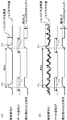
- FIG. 1 is a block diagram illustrating a configuration of a receiving device according to the first embodiment.
- the transmitter Tx is also shown for convenience of explanation.
- the receiving device Rx uses a short pulse wave transmitted from the transmitting device Tx at a preset transmission interval of a predetermined time, and uses an ultra-wideband communication method (hereinafter, “ For example, the antenna 1, the amplification unit 2, the pulse extraction unit 3, the bit determination unit 4, and the transmission signal information are subjected to predetermined signal processing. And a transmission signal information processing unit (not shown) for processing.
- the antenna 1 is a device that receives a UWB communication type radio signal transmitted from the transmission device Tx, and converts a radio signal of a radio wave into a reception signal of an electric signal.
- the amplification unit 2 is a circuit that is connected to the antenna 1 and amplifies a reception signal output from the antenna 1 with a predetermined amplification factor, and includes, for example, a low noise amplifier.
- the antenna 1 and the amplifying unit 2 are provided before the pulse extracting unit 3.
- the pulse extraction unit 3 is connected to the amplification unit 2 and includes an expander 31, a filter 32, and a pulse detector 33.
- the expander 31 is a circuit that is connected to the amplification unit 2 and converts the frequency of the reception signal Sr obtained by receiving the radio signal transmitted from the transmission device Tx by the antenna 1 and outputs the intermediate signal Sa. .
- the expander 31 includes, for example, an oscillator 31a and a mixer 31b.
- the oscillator 31a is an oscillation circuit that outputs a local oscillation signal So having a frequency f2 having a sufficiently large frequency difference with respect to the frequency f1 of the reception signal Sr (the frequency f1 is the center frequency of the reception signal Sr). 31a is subjected to frequency control and timing control by a pulse detector 33.
- the frequency f2 is a frequency (f2 ⁇ f1) lower than the frequency f1, and has a frequency difference of, for example, several hundred MHz or more, more specifically, for example, 1 GHz or more with respect to the frequency f1. More specifically, from the viewpoint of easy design, for example, the intermediate signal Sa has the same bandwidth as the intended short pulse wave (see FIG. 2A), and the filter 32
- the frequency f2 of the local oscillation signal So output from the oscillator 31a is set so that the upper limit of the pass band is lower than the lower limit frequency of the target short pulse wave.
- the mixer 31b is a circuit that is connected to the amplifying unit 2 and the oscillator 31a, and mixes the signals Sr and So by multiplying the reception signal Sr and the local oscillation signal So to output an intermediate signal Sa.
- the received signal Sr (frequency f1) is down-converted by the expander 31 and becomes an intermediate signal Sa (frequency f1-f2, frequency f1 + f2).
- the filter 32 is connected to the mixer 31 b of the expander 31 and is provided in the subsequent stage of the expander 31.
- a predetermined frequency range is preset as a pass band for the intermediate signal Sa output from the expander 31, and the predetermined frequency range of the intermediate signal Sa output from the expander 31 is set. Is passed as an intermediate signal Sb.
- the filter 32 is band-controlled and timing-controlled by the pulse detector 33.
- the filter 32 includes, for example, a band pass filter (BPF).
- BPF band pass filter
- the intermediate signal Sa is filtered (filtered) by the filter 32 to become an intermediate signal Sb (frequency f1-f2).
- the pulse detector 33 is connected to the filter 32, and identifies the pulse and the pulse position based on the intermediate signal Sb output from the filter 32 (identification of the pulse position on the time axis, identification of the arrival time of the pulse). To output a pulse detection signal Sc.
- the bit determination unit 4 is connected to the pulse extraction unit 3 and extracts a bit value of a radio signal transmitted from the transmission device Tx based on the pulse detection signal Sc output from the pulse detector 33 of the pulse extraction unit 3
- the output of the bit determination unit 4 is used by the transmission signal information processing unit (not shown) as data received from the transmission device Tx.
- the bit determination unit 4 is provided in the subsequent stage of the pulse extraction unit 3.
- the following operation is performed in the receiving device Rx having such a configuration.
- FIG. 2 is a diagram for explaining signal waveforms of respective units in the receiving apparatus shown in FIG.
- FIG. 2A shows a schematic waveform of the reception signal Sr obtained by receiving the radio signal transmitted from the transmission device Tx
- FIG. 2B shows a time chart of the transmission window Wt.
- FIG. 3 shows a diagram for explaining frequency conversion of the expander in the receiving apparatus shown in FIG.
- FIG. 3A shows a case where the reception signal Sa having the frequency f1 and the local oscillation signal So having the frequency f2 are mixed
- FIG. 3B shows the reception signal Sa having the frequency f1 and the fundamental frequency f3 that is not a sine wave. This shows a case where the local oscillation signal So is mixed.
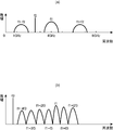
- the radio signal transmitted from the transmitter Tx is composed of ultrashort pulse waves of 1 ns (nanoseconds) or less, but each ultrashort pulse wave is actually a burst wave as shown in FIG. .
- the burst wave has a duration of about 2 ns, a period of 1 ns or less, for example, about several hundred ps, and its amplitude gradually increases with the passage of time and gradually reaches a peak. Has decreased.
- the frequency of the ultrashort pulse wave used in the UWB communication system means the reciprocal of the period.
- the ultrashort pulse wave is transmitted from the transmission device Tx at a transmission interval of a predetermined time set in advance, for example, to 30 ns or 57 ns.
- the phase information is not used in the present embodiment in order to distinguish the data value (bit value), and as shown in FIG.
- the presence / absence of an ultrashort pulse wave in a certain transmission window Wt is used as a bit value.
- the bit value is 1 when an ultrashort pulse wave exists in the transmission window Wt, and the bit value is 0 when no ultrashort pulse wave exists in the transmission window Wt.
- the bit value may be determined based on the level difference of the detected value between the section with the pulse and the section without the pulse, using a so-called Manchester code or the like. By such an operation, non-coherent communication can be performed without using phase information.
- the reception signal Sr is processed by the expander 31 and the filter 32 before the reception signal Sr output from the amplification unit 2 is input to the pulse detector 33.
- the oscillator 31a provided in the expander 31 has a sufficiently large frequency difference with respect to the frequency f1 of the reception signal Sr, and has a waveform that does not depend on the phase and waveform of the ultrashort pulse wave included in the reception signal Sr.
- the expander 31 can output the intermediate signal Sa without depending on the ultrashort pulse wave and each phase of the local oscillation signal So. Configuration is realized.
- the frequency f2 of the local oscillation signal So output from the oscillator 31a is set to be lower than the frequency f1 of the reception signal Sr (f1> f2).
- the frequency f2 of the local oscillation signal So is set higher than the frequency f1 of the reception signal Sr.
- the oscillator 31a can be easily designed. When data is transmitted non-coherently, the phase difference between the reception signal Sr and the local oscillation signal Sa is irrelevant.
- the frequency of the intended ultrashort pulse wave is set to the frequency f1 and Assuming that the frequency of the local oscillation signal So is the frequency f2, the intermediate signal Sa output from the expander 31 has a frequency (f1 + f2) and a frequency (f1-f2) as shown in FIG. ) Frequency components are included.
- a (t) A ⁇ sin ( ⁇ 1 ⁇ t)
- b (t) B ⁇ sin ( ⁇ 2 ⁇ t)
- a (t) is the received signal Sr
- b (t) is the local signal So
- a and B are the amplitude of the received signal Sr and the local signal So, respectively
- the received signal Sr is frequency-converted from the frequency f1 to a frequency (f1-f2) lower by the frequency f2. That is, by passing the output of the mixer 31b of the expander 31 through the filter 32 and setting the passband characteristic of the filter 32 so that the frequency component (f1-f2) passes and the frequency component (f1 + f2) does not pass, The frequency f1 of the signal Sr is down-converted to the frequency (f1-f2).
- the supply current to the transistor becomes relatively large as the frequency increases, and the power consumption becomes relatively large.
- the frequency is lowered by the expander 31 as described above, so that low power consumption can be achieved even during the driving period of intermittent driving. Can be realized.
- the receiving device Rx is driven by a battery such as a primary battery or a secondary battery, such low power consumption is effective and advantageous.
- At least one of the signal level of the local signal So output from the oscillator 31a and the signal level of the intermediate signal Sa output from the mixer 31b is variable stepwise or continuously. It has become. More specifically, a second amplifier 31d (shown by a broken line) that amplifies the local signal So output from the oscillator 31a and a first amplifier 31c (shown by a broken line) that amplifies the intermediate signal Sa output from the mixer 31b. At least one of them is provided, and the amplification factor of the provided amplifier can be adjusted by a gain control signal output from the pulse detector 33. When both amplifiers are provided, the amplification factors of these provided amplifiers are individually determined by gain control signals (first gain control signal and second gain control signal) output from the pulse detector 33. It can be adjusted.
- gain control signals first gain control signal and second gain control signal
- the signal level (A ⁇ B / 2) of the intermediate signal Sa output from the mixer 31b is changed by changing the amplitude B of the local signal So input from the oscillator 31a to the mixer 31b. ) Is changed.
- the SNR signal-to-noise ratio
- the level difference can be used by optimizing the amplification factor to easily separate them. Can be done. For example, by setting an appropriate threshold value for the signal level, an ultrashort pulse wave and an interference wave or an unnecessary wave can be separated.
- the passband characteristic of the filter 32 can be lowered below the frequency f1 of the received signal Sr by performing the down-conversion with the expander 31.
- the filter circuit 32 has a lower frequency than the frequency f1 of the received signal Sr as the filter 32 (where the frequency f1 has a bandwidth corresponding to the passband of the filter 32 instead of a single frequency).
- the pass band of the filter 32 can be lowered as compared with the case where the expander 31 is not used.
- the pass band of the filter 32 can be greatly reduced.
- the center frequency f1 of the received signal Sr is 4 GHz and the frequency f2 of the local signal So is 2.6 GHz
- the center frequency of the pass band of the filter 32 may be 1.4 GHz. it can.
- the oscillator 31a of the expander 31 outputs the sine wave local signal So, but is not limited to a circuit that outputs the sine wave local signal So, and the local signal So is The sine wave may not be used.
- the local oscillation signal So having a waveform that is not a sine wave is used, an intermediate signal of the frequency difference between the reception signal Sr and the harmonic component of the local oscillation signal So is also obtained at the output of the mixer 31b.
- the basic frequency of the local signal So is f3
- the frequency f1 of the received signal Sr and the basic frequency of the local signal So are f3. For example, as shown in FIG.
- the filter 32 can be configured by using a high-frequency circuit technology and an electronic device that are used for a mobile phone, a wireless LAN, and the like.
- the filter 32 can be designed more easily than when the filter 32 having a center frequency of 4 GHz or more is configured. For this reason, an expander 31 is provided in front of the filter 32. There may be another circuit between the expander 31 and the filter 32.
- the filter 32 can be configured by a combination of a wide bandpass filter of 500 MHz or more as a whole and a notch filter (band elimination filter, band elimination filter) that attenuates a specific frequency band. Therefore, the filter 32 is configured by combining an active element with a resonance circuit.
- a microstrip line and a ceramic filter are used.
- a filter having a center frequency of 4 GHz or more it is necessary to use an individual element as an active element.
- an operational amplifier op amp
- Such an integrated circuit can be used. Therefore, the filter 32 can be integrated and the size and cost can be reduced.
- the filter 32 can adjust the center frequency and bandwidth as a band pass filter and the center frequency and bandwidth as a notch filter by a band control signal output from the pulse detector 33. That is, the pass band of the filter 32 can be adjusted by the band control signal. For this adjustment, a plurality of predetermined resonance circuits are provided in the filter 32, and one of the plurality of resonance circuits is selected from the plurality of resonance circuits by the band control signal output from the pulse detector 33. A configuration that changes in stages can be adopted.
- an electronic device whose capacitance can be adjusted by an external signal, such as a variable capacitance diode, is provided in the filter 32 in the resonance circuit, and the capacitance is output by the band control signal output from the pulse detector 33 as the external signal. It is also possible to adopt a configuration in which the frequency is continuously changed by adjusting.
- the pulse detector 33 controls the pass band of the filter 32, the pass band of the filter 32 so that the frequency of the intermediate signal Sa corresponding to the interference wave and the unnecessary wave is excluded from the filter pass band.
- the influence of interference waves and unnecessary waves can be reduced.
- the passband of the filter 32 By adjusting the passband of the filter 32 by using the band control signal, the signal level of the intermediate signal corresponding to the target ultrashort pulse wave can be relatively increased in the pulse detector 33. .
- a reception period Wr corresponding to the transmission window Wt set in the transmission device Tx is set.
- the bit is set when the radio signal of the ultrashort pulse wave is received in the set reception period Wr.
- a value of 1 is output from the bit determination unit 4, and a bit value of 0 is output from the bit determination unit 4 when no radio signal of an ultrashort pulse wave is received in the set reception period Wr.
- the reception period Wr in the receiving device Rx may be a time width equal to or longer than one cycle of the ultrashort pulse wave. As the time width of the reception period Wr increases, it becomes more susceptible to interference of other signals. On the other hand, as the time width of the reception period Wr decreases, the transmission window Wt of the transmission device Tx and the reception period Wt of the reception device Rx are synchronized. It will take time. Accordingly, it is desirable that the time width of the reception period Wr set in the reception device Rx is set to about 2 to 5 times the transmission window Wt.
- the pulse detector 33 has a function of controlling the output period of the local signal So by outputting a timing control signal from the oscillator 31a. For example, as shown in FIG. 2D, the pulse detector 33 controls the oscillator 31a to output the local oscillation signal So from the oscillator 31a only in the reception period Wr (in synchronization with the reception period Wr). By controlling the oscillator 31a to operate the oscillator 31a), as shown in FIG. 2 (e), the intermediate signal Sb generated when the target ultrashort pulse wave passes through the filter 32 is The reception pulse P is generated at a predetermined cycle.
- the reception pulse P is generated by, for example, a detector configured by including a square detector, an absolute value circuit, and the like, and performing envelope detection for extracting the envelope on the intermediate signal Sb. Corresponds to the envelope of an ultra-short pulse wave.
- the oscillator 31a does not always operate according to the timing control signal of the pulse detector 33, thereby reducing the power consumption of the receiving device Rx.
- the filter 32 has a pass band set so as to allow the intermediate signal Sa to pass therethrough and not to pass interference waves and unnecessary waves (hereinafter referred to as “interference waves”), and the reception period as described above.
- the oscillator 31a is controlled so as to output the local signal So from the oscillator 31a only at Wr. Thereby, even when an interference wave or the like within the frequency range of the ultrashort pulse wave is received in a period that is not the reception period Wr, the expander 31 does not frequency-convert the frequency f1 of the reception signal Sr to the passband of the filter 32.
- the output of the expander 31 is not frequency-converted to the pass band of the filter 32, the output of the expander 31 cannot pass through the filter 32, and interference waves and the like are removed from the output of the filter 32. can do.
- the interference wave or the like is received in the reception period Wr and the frequency of the interference wave or the like is included in the frequency range of the target ultrashort pulse wave, the interference wave or the like and the target ultrashort pulse wave Can not be distinguished.
- this type of interference wave or the like can be removed by setting the pass band of the filter 32 so as to remove the frequency component such as the interference wave that has been confirmed to exist in the usage environment of the receiving device Rx. It is.
- the pulse detector 33 has a function of outputting a timing control signal to the filter 32 to control the operation period of the filter 32.
- the pulse detector 33 controls the filter 32 so as to output the intermediate signal Sb obtained by filtering the intermediate signal Sa only in the reception period Wr (the filter 32 so as to operate the filter 32 in synchronization with the reception period Wr).
- the filter 32 does not always operate, thereby reducing the power consumption of the receiving device Rx.
- the pulse detector 33 includes an integration unit 33a that integrates the intermediate signal Sb output from the filter 32 in an integration period synchronized with the reception period Wr, and compares the integration value with a predetermined threshold value to determine a binary level. And a level determination unit 33b that outputs a determination result, and performs identification and position identification (arrival time identification) of the received pulse P included in the intermediate signal Sb output from the filter 32, thereby achieving a target pulse.
- a target ultrashort pulse wave is distinguished from an interference wave or the like, it is referred to as a “target wave”
- the extracted pulse is output to the bit determination unit 4 as a pulse detection signal Sc.
- the integration unit 33a and the level determination unit 33b (or at least one of the integration unit 33a and the level determination unit 33b) operate only in the reception period Wr, thereby reducing the power consumption of the reception device Rx. .
- the pulse detector 33 has a function of supplying a timing control signal to the oscillator 31a and the filter 32 to control the operation period, and the oscillator 31a and the filter 32 have the reception period Wr (that is, , Intermittent operation in synchronism with the generation timing of a short pulse included in the reception signal Sr). Furthermore, in this embodiment, the integration unit 33a and the level determination unit 33b of the pulse detector 33 also operate intermittently in synchronization with the reception period Wr. For this reason, in the reception period Wr, the power consumption of the reception device Rx is suppressed, and the power consumption of the reception device Rx is reduced.
- the pulse detector 33 not only outputs the gain control signal to the expander 31, the band control signal to the filter 32, and the timing control signal to the oscillator 31a and the filter 32, as described above. It has a function of outputting a period control signal by controlling the expander 31 to determine the reception period Wr, and a function of adjusting the frequency f2 of the local signal So by outputting a frequency control signal to the oscillator 31a. Also good.
- frequency control of the oscillator 31a will be described.
- FIG. 4 is a diagram showing a configuration of an oscillator in the receiving apparatus shown in FIG.
- FIG. 5 is a diagram for explaining a local oscillation signal generated by the oscillator shown in FIG.
- FIG. 6 is a circuit diagram showing a configuration of a delay line circuit in the oscillator shown in FIG.
- FIG. 7 is a diagram for explaining the delay of the clock signal generated by the delay line circuit shown in FIG.
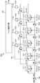
- an oscillator 31a with a frequency control function includes a plurality of toggle flip-flops 1010 to 101n, a plurality of XOR elements 1021 to 102n, a plurality of AND elements 1031 to 103n, and a plurality of delay line circuits 1041 to 104n.
- a pulse selection circuit 105 and a delay line circuit 106 are provided.
- FIG. 4 shows five toggle flip-flops 1010 to 1014, four XOR elements 1021 to 1024, four AND elements 1031 to 1034, four delay line circuits 1041 to 1044, and a pulse selection circuit 105. ing.
- the reception device Rx synchronizes the reception period Wr with the transmission window Wt of the transmission device Tx and performs communication in the UWB communication system.
- the clock signal is delayed and the rising timing of the clock signal is delayed.
- the toggle flip-flop 1010 receives a clock signal CLK from a clock generator (not shown) via the delay line circuit 106, and the toggle flip-flop 1010 outputs the clock signal CLK0 generated according to the clock signal CLK to the XOR element 1021. To do.
- a clock signal CLK is input to the toggle flip-flop 1011 from the clock generator (not shown) via the delay line circuit 106 and the delay line circuit 1041, and the toggle flip-flop 1011 is generated according to the output of the delay line circuit 1041.
- the clock signal CLK1 is output to the XOR element 1021, AND element 1031 and XOR element 1022, respectively.
- Clock signal CLK 0 and clock signal CLK 1 are input to XOR element 1021, and XOR element 1021 outputs an exclusive OR of clock signal CLK 0 and clock signal CLK 1 to AND element 1031.
- the AND element 1031 receives the clock signal CLK1 and the output of the XOR element 1021, and the AND element 1031 outputs a logical product of the clock signal CLK1 and the output of the XOR element 1021 to the pulse selection circuit 105 as a signal S1.
- the clock signal CLK is input to the toggle flip-flop 1012 from the clock generator (not shown) via the delay line circuit 106, the delay line circuit 1041, and the delay line circuit 1042, and the toggle flip-flop 1012 is connected to the delay line circuit 1042.
- Clock signal CLK2 generated according to the output is output to XOR element 1022, AND element 1032 and XOR element 1023, respectively.
- Clock signal CLK 1 and clock signal CLK 2 are input to XOR element 1022, and XOR element 1022 outputs an exclusive OR of clock signal CLK 1 and clock signal CLK 2 to AND element 1032.
- the AND element 1032 receives the clock signal CLK2 and the output of the XOR element 1022, and the AND element 1032 outputs a logical product of the clock signal CLK2 and the output of the XOR element 1022 to the pulse selection circuit 105 as a signal S2.
- the toggle flip-flop 1013 receives the clock signal CLK from the clock generator (not shown) via the delay line circuit 106, the delay line circuit 1041, the delay line circuit 1042, and the delay line circuit 1043.
- the toggle flip-flop 1013 Clock signal CLK3 generated according to the output of delay line circuit 1043 is output to XOR element 1023, AND element 1033, and XOR element 1024, respectively.
- Clock signal CLK 2 and clock signal CLK 3 are input to XOR element 1023, and XOR element 1023 outputs an exclusive OR of clock signal CLK 2 and clock signal CLK 3 to AND element 1033.
- the AND element 1033 receives the clock signal CLK3 and the output of the XOR element 1023, and the AND element 1033 outputs the logical product of the clock signal CLK3 and the output of the XOR element 1023 to the pulse selection circuit 105 as a signal S3.
- the toggle flip-flop 1014 receives the clock signal CLK from the clock generator (not shown) via the delay line circuit 106, the delay line circuit 1041, the delay line circuit 1042, the delay line circuit 1043, and the delay line circuit 1044.
- the toggle flip-flop 1014 outputs the clock signal CLK4 generated according to the output of the delay line circuit 1044 to the XOR element 1024, the AND element 1034, and the XOR element 1025 (not shown).
- Clock signal CLK 3 and clock signal CLK 4 are input to XOR element 1024, and XOR element 1024 outputs an exclusive OR of clock signal CLK 3 and clock signal CLK 4 to AND element 1034.
- the AND element 1034 receives the clock signal CLK4 and the output of the XOR element 1024.
- the AND element 1034 outputs a logical product of the clock signal CLK4 and the output of the XOR element 1024 to the pulse selection circuit 105 as a signal S4.
- the clock signal CLK is sequentially input to the toggle flip-flop 101n from the clock generator (not shown) via the delay line circuit 106 and the delay line circuit 1041 to the delay line circuit 104n-1.
- the flip-flop 101n outputs the clock signal CLKn generated according to the output of the delay line circuit 104n-1 to the XOR element 102n, the AND element 103n, and the XOR element 102n + 1.
- Clock signal CLKn-1 and clock signal CLKn are input to XOR element 102n, and XOR element 102n outputs an exclusive OR of clock signal CLKn-1 and clock signal CLKn to AND element 103n.
- the AND element 103n receives the clock signal CLKn and the output of the XOR element 102n.
- the AND element 103n outputs a logical product of the clock signal CLKn and the output of the XOR element 102n to the pulse selection circuit 105 as a signal Sn.
- the oscillator 31a includes a toggle flip-flop 101, an XOR element 102, an AND element 103, and a delay line circuit 104, and a plurality of signal generation circuits 100 that generate a signal S are connected in cascade.
- the output of the delay line circuit 101k-1 in the previous signal generation circuit 100k-1 is input to the delay line circuit 101k in the signal generation circuit 100k of the current stage.
- the output of the delay line circuit 101k is input to the toggle flip-flop 101k and the delay line circuit 104k + 1 in the next-stage signal generation circuit 100k + 1.
- the toggle flip-flop 101k generates a clock signal CLKk according to the output of the delay line circuit 101k, and outputs this clock signal CLKk to the XOR element 102k and the XOR element 102k in the next-stage signal generation circuit 101k + 1.
- the XOR element 102k includes the output of the toggle flip-flop 101k-1 in the previous-stage signal generation circuit 101k-1 (clock signal CLKk-1 in the previous-stage signal generation circuit 101k-1) and the output of the toggle flip-flop 101k (the current signal in this stage).
- An exclusive OR with the clock signal CLKk) in the generation circuit 101k is output to the AND element 103k.
- the AND element 103k outputs a logical product of the output of the toggle flip-flop 101k and the output of the XOR element 102k to the pulse selection circuit 105 as a signal Sk.
- the clock signal CLK is input to the delay line circuit 1041 from the clock generator (not shown) via the delay line circuit 106, and is generated by the clock generator and delayed by the delay line circuit 106.
- the clock signal CLK 0 is generated by the toggle flip-flop 1010 in accordance with the clock signal CLK thus input, and this clock signal CLK 0 is input to the XOR element 1021.
- preset signals and presets are appropriately input to the toggle flip-flops 1010 to 101n.
- the pulse selection circuit 105 combines the waveforms of the signals S1 to Sn based on the frequency control signal output from the pulse detector 33 to generate a local signal So having a desired waveform (or frequency).
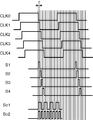
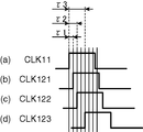
- FIG. 5 shows a clock signal CLK0 to a clock signal CLK4, a signal S1 to a signal S4, and local signals So1 and So2 in order from the top to the bottom.
- the clock CLK0 shown in FIG. 5 is a signal via the delay line circuit 106.
- the local signals So1 and So2 are examples of generating the local signal So generated by the oscillator 31a shown in FIG.
- a delay time ⁇ is generated by the delay line circuit 1041 through the delay line circuit 104n between the clock signal CLK0 through the clock signal CLKn.
- the delay time of each of the delay line circuits 1041 to 104n is time ⁇
- the clock signal CLKn becomes a delayed clock signal with respect to the preceding clock signal CLKn ⁇ 1
- the clock signal CLKn is converted to the preceding clock signal CLKn ⁇ . 1 is delayed by a delay time ⁇ .
- the signals S1 to Sn are pulses whose pulse width is the delay time ⁇ and are sequentially shifted by the delay time ⁇ , as shown in FIG. Therefore, for example, by using two signals S1 to Sn every two, a pulse-like local signal So1 having a pulse width of 2 ⁇ ⁇ and a period of 4 ⁇ ⁇ is generated. By using the signals S1 to Sn one by one, a pulse-like local signal So2 having a pulse width of ⁇ and a period of 2 ⁇ ⁇ is generated.
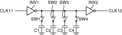
- the delay line circuit 104 (1041 to 104n) includes two inverter elements INV1 and INV2, and one or a plurality of series circuits including a capacitor C and a switch SW.
- the output of one inverter element INV1 is connected to the input of the other inverter element INV2, and one or more series circuits are connected between the output of the inverter element INV1 and the ground level.
- four series circuits (capacitors C1 to C4, switches SW1 to SW4) are connected.
- the switches SW1 to SW4 of each series circuit are on / off controlled by a frequency control signal output from the pulse detector 33.
- the capacitance connected to the output of the inverter element INV1 is changed by the on / off control of the switches SW1 to SW4, and is input to the delay line circuit 104 as shown in FIGS. 7A to 7D, for example.
- a delay time ⁇ (see FIG. 5) due to the capacitance occurs.
- the capacitances of the capacitors C1 to C4 are C, 2C so that the capacitances of 0, C, 2C, 3C,. 4C, 8C.
- the clock signal CLK12 output from the delay line circuit 104 is as shown in FIG. 7B with respect to the clock signal CLK11.
- the lock signal CLK123 when only the switch SW1 is on, the clock signal CLK12 output from the delay line circuit 104 is as shown in FIG. 7B with respect to the clock signal CLK11.
- the pulse selection circuit 105 combines the waveforms of the signals S1 to Sn with the frequency control signal output from the pulse detector 33, and controls the delay time ⁇ of the delay line circuit 104, thereby generating a local signal.
- the waveform of So and the frequency f2 are arbitrarily controlled.
- the oscillator 31a is constituted by a relatively simple circuit as shown in FIG. 4, and low power consumption is possible. Further, since the frequency of the local signal So can be adjusted according to the frequency of the transmission signal, it is possible to deal with a plurality of transmission signals having different frequencies.
- the oscillator 31a may be configured using a PLL (Phase-Looked Loop) circuit.
- FIG. 8 is a block diagram showing a configuration of a PLL circuit that can be used in the oscillator in the receiving apparatus shown in FIG.
- the PLL circuit generally includes a series circuit of a phase comparator 111, a charge pump 112, a loop filter 113 and a voltage controlled oscillator 114, and a feedback path from the output of the voltage controlled oscillator 114 to the phase comparator 111. And a frequency divider 115 provided in the circuit.
- the output of the voltage controlled oscillator 114 is the local oscillation signal So, and the delay line circuit 104 is configured by at least a part of the PLL circuit, so that a general PLL circuit is used for the oscillator 31a.
- This is advantageous in terms of cost.
- DLL Delay-Looked Loop, delay locked loop
- FLL Frequency-Looked Loop, frequency locked loop
- the frequency f2 of the local oscillation signal So output from the oscillator 31a is adjustable in this way, the frequency f2 of the local oscillation signal So is set so that an intermediate signal such as an interference wave is outside the pass band of the filter 32. It becomes possible to adjust, and it is highly possible that interference waves and the like can be removed by such adjustment. That is, the influence of interference waves and the like can be reduced. In the pulse detector 33, it is also possible to adjust the frequency f2 of the local oscillation signal So so that the signal level of the intermediate signal corresponding to the target wave is increased. Furthermore, it is desirable that the frequency control signal to the oscillator 31a and the band control signal to the filter 32 described above are controlled in conjunction with each other. In particular, since the center frequency of the notch filter for removing the interference wave and the like needs to match the intermediate signal related to the interference wave, it is desirable to link the frequency control signal and the band control signal.
- the pulse extraction unit 3 of the present embodiment in order to separate the interference wave and the like from the target wave, a technique for setting the reception period Wr according to the target wave, the interference wave and the like
- the technique of separating the frequency band in which the interference wave exists from the target wave and the technique of separating the interference wave etc. by the level difference of the signal level between the interference wave and the target wave are used in combination. That is, the pulse extraction unit 3 limits the time for extracting the target wave from the received signal Sr, thereby reducing the power consumption of the receiving device Rx and the interference wave generated at a time different from the target wave. Is removed, and interference waves and the like generated at substantially the same time as the target wave are removed by utilizing the difference in frequency components and the difference in signal level.
- the pulse extraction unit 3 In the pulse extraction unit 3, interference waves and the like are physically removed, but the interference waves and the like are not completely removed. For this reason, when the output of the pulse extraction unit 3 is logically determined by the bit determination unit 4 and the bit value extracted by the pulse extraction unit 3 is not correct, the data is discarded. Whether the bit value is correct or not is determined by inserting a bit synchronization pulse train SB (see FIG. 9) before data when transmitting a radio signal from the transmission device Tx, and receiving the bit synchronization pulse train SB in the reception device Rx (bit determination unit 4). Can be confirmed by checking The bit determination unit 4 can also confirm whether the bit value is correct by using a code error detection technique such as a so-called checksum. When the data is discarded, a known communication process such as a retransmission request is performed.
- a code error detection technique such as a so-called checksum
- FIGS. 9A and 9B are diagrams illustrating a frame configuration in a radio signal of the UWB communication method.
- the reception period Wr is determined, for example, so that the timing at which the transmission device Tx generates the target wave coincides with the timing at which the reception device Rx generates the local oscillation signal So from the oscillator 31a.
- a state in which both timings coincide with each other corresponds to that the transmission device Tx and the reception device Rx operate in synchronization in transmission / reception of a communication signal of the UWB communication method.
- one frame of a radio signal transmitted from the transmission device Tx includes, for example, a synchronization pulse train SY as shown in FIG.
- the frame also includes the bit synchronization pulse train SB used in the bit determination unit 4 as described above.
- the frame includes a data pulse train DT after the synchronization pulse train SY and the bit synchronization pulse train SB.
- the pulse detector 33 of the reception device Rx sets the timing of the reception period Wr so as to synchronize with the transmission device Tx using the synchronization pulse train SY shown in FIG. 9B.
- an ultrashort pulse wave is used as in the data pulse train DT.
- the bit value is represented by the presence or absence of a train of ultrashort pulse waves in the transmission window Wt.
- an ultrashort pulse wave is generated at a constant period so that a train of ultrashort pulse waves exists in all the transmission windows Wt.
- the pulse detector 33 operates in a search mode for searching for the start timing of the reception period Wr.
- this search mode the time interval for providing the reception period Wr is changed, and the reception timing of the synchronization pulse train SY is detected.
- This time interval is set shorter than the time interval at which the transmission window Wt is generated. For example, the time interval for providing the reception period Wr is changed every time, and the synchronization reception pulse train SY is received by appropriately setting the number of synchronization pulse trains SY and the time interval of the reception period Wr.
- any reception period Wr frequency conversion of the ultrashort pulse wave included in the synchronization pulse train SY is performed, and the intermediate signal Sb corresponding to the ultrashort pulse wave is obtained from the filter 32.
- the pulse detector 33 compares the integral value of the intermediate signal Sb (see FIG. 2 (e)) output from the filter 32 with a predetermined threshold, and an intermediate signal whose signal level has not reached the predetermined threshold is: Excluded as interference waves.
- the pulse detector 33 may generate an interference wave or the like generated by the system from an intermediate signal whose integrated value does not reach the predetermined threshold value.
- An interference wave detection unit that detects an interference wave and outputs an interference wave detection signal may be further provided, which makes it possible to distinguish between the intended ultrashort pulse wave and the interference wave.
- the pulse detector 33 acquires data from the search mode.
- the time interval of the reception period Wr after the reception period Wr is switched to a time interval that substantially matches the time interval at which the transmission window Wt is generated in the transmission device Tx. With this operation, the transmission device Tx and the reception device Rx can be synchronized.
- the pulse detector 33 compares the integral value for each reception period Wr with a threshold value, and outputs the magnitude relationship between the integral value and the threshold value as the pulse detection signal Sc.
- a pulse detection signal Sc composed of a signal corresponding to a bit value of 1 is output, and when the integral value is smaller than the threshold value, it comprises a signal corresponding to a bit value of 0. A pulse detection signal Sc is output.
- the pulse detector 33 identifies the position of the pulse that matches the reception period Wr in the search mode, that is, identifies the time when the transmission device Tx generated the transmission window Wt, and in the data mode, detects the pulse at that position. Identify presence or absence.
- the position is a position on the time axis (temporal position).
- the pulse detector 33 normally operates in the search mode in which the time interval of the reception period Wr is changed.
- the transmission device Tx Until one frame of the radio signal transmitted from is completed, the operation is performed in the data mode in which the reception period Wr matches the time interval at which the transmission window Wt is generated.
- the end of one frame of the radio signal is determined, for example, by detecting a sequence indicating the end of the frame and notifying the end of the frame from the bit determining unit 4. Further, for example, this end is determined when the state where the pulse detection signal Sc is not generated reaches a predetermined specified time.
- the timing of the drive period (oscillation period, reception period Wr) in the oscillator 31a and the time width of the drive period are provided by supplying a timing control signal to the expander 31. At least one of them is controlled.
- the bit determination unit 4 stops operating until the ultrashort pulse wave is detected in the search mode, and performs the determination operation until one frame of the radio signal is completed after the ultrashort pulse wave is detected. Later, the operation is stopped again. Thus, since the bit determination unit 4 operates only when necessary, the power consumption of the receiving device Rx can be reduced.
- the transmitting device Tx and the receiving device Rx are provided with at least time measuring means (not shown) for measuring the time interval, and both time measuring means have such accuracy that an error can be ignored within the time required for transmission of one frame. ing.
- the pulse detector 33 only needs to be able to extract the target wave, and it is not necessary to use all of the intermediate signal Sb that has passed through the filter 32. Therefore, the frequency of the intermediate signal Sb is High stability is not required. Therefore, high stability is not required also for the frequency f2 of the local oscillation signal So output from the oscillator 31a, and the design is facilitated from this.
- FIG. 10 is a diagram for explaining the object detection operation of the receiving apparatus according to the second embodiment.
- FIG. 11 is a diagram for explaining an object detection operation in consideration of multipath of the receiving device according to the second embodiment.
- FIG. 11A is a diagram for explaining object detection by multipath, and
- FIG. 11B is a diagram for explaining a scanning method of the receiving device Rx.
- the receiving device Rx according to the second embodiment is configured such that a UWB transmission signal is a short pulse wave arranged at regular intervals instead of a non-coherent communication signal for transmitting data.
- a UWB transmission signal is a short pulse wave arranged at regular intervals instead of a non-coherent communication signal for transmitting data.
- the receiving device Rx has a receiving period Wr as shown in FIG. 10 when the transmitting device Tx transmits a short pulse wave at the predetermined time interval (short pulse wave transmission interval).
- the reception period Wr is scanned by sequentially shifting (the integration start time of the integrator 33a) at a predetermined time interval, and each integration value of the integrator 33a and a predetermined threshold value (in the reception period Wr obtained by this scanning) And the elapsed time from the emission time of the short pulse wave corresponding to the reception period Wr that gives the integrated value of the integrator 33a that is equal to or greater than the predetermined threshold (object detection threshold) as a result of the comparison. Based on the above, the distance to the object is calculated.
- the emission time of the short pulse wave is set to time 0
- the integral value of the integrator 33a in the reception period Wr at time t2 is equal to or greater than the predetermined threshold
- the pulse detector 33 measures the integral value of the integrator 33a a plurality of times in a certain reception period Wr, and based on the dispersion value of each integral value by these measurements. It is also possible to detect the presence or absence of motion of the object. That is, the receiving device Rx of the second embodiment outputs a pulse detection signal that outputs a pulse detection signal by identifying a target pulse and an arrival time from the intermediate signal, and outputs the pulse detection signal from the pulse detector 33.
- An object motion detector (not shown) that detects the presence or absence of motion of the object based on a pulse detection signal, and the pulse detector 33 detects a reflected wave from the object at the arrival time at which the target pulse is identified.
- the object motion detection unit moves the object based on a dispersion value of each received intensity obtained by receiving the reflected wave a plurality of times.
- the presence or absence of is detected.
- the short pulse wave radiated from the transmission device Tx always strikes the object and a nearby stationary object in substantially the same manner, and thus is received by the reception device Rx. Since the reception intensity of the reflected wave is substantially constant, the dispersion value of each integral value of the integrator 33a in a certain reception period Wr is relatively small. In the case of the present embodiment, the dispersion of the power intensity of the reflected wave is detected. This dispersion is a composite wave obtained by simultaneously receiving the reflected wave of a nearby stationary object and the reflected wave of each detailed part of the moving object. Caused by fluctuations in amplitude intensity.
- the receiving device Rx first detects an object preliminarily by the above-described operation using the object detection threshold, and further sets a plurality of integration values of the integrator 33a in the reception period Wr in which the object is detected.
- the dispersion value of each integral value obtained by each measurement is compared with a predetermined threshold value (object motion detection threshold value). As a result of this comparison, the variance value is equal to or greater than the predetermined threshold value (object motion detection threshold value). In some cases, it is possible to take means for determining the presence of an object in which an object detected using this object detection threshold is moving.
- the receiving device Rx may be configured to measure the integral value of the integrator 33a a plurality of N times in each reception period Wr in order to collectively detect the object and the motion of the object. .
- the intensity of the reflected wave from the object is usually small.
- the reception device Rx uses the integrator 33a in the reception period Wr.
- the integration value of the integrator 33a may be measured by performing integration for K times. Therefore, when performing the plurality of N times of measurement and the integration of the plurality of K times, the transmission device Tx transmits a plurality of N ⁇ K times of the short pulse wave.
- the transmission device Tx and the reception device Rx in the second embodiment constitute an object detection system that detects the distance to the object and the motion of the object in an active manner.
- detection is performed based on the intensity of a reflected wave from the object, so that the receiving device Rx directly integrates the reflected wave. It is difficult to distinguish the integration value of the integrator 33a from the integration value of the integrator 33a obtained by receiving the reflected wave by multipath. That is, the receiving device Rx directly reflects the short pulse wave radiated from the transmitting device Tx on the object and is reflected by the object, and the reflected value is directly received by the receiving device Rx.
- the receiving device Rx according to the second embodiment moves away from the receiving device Rx as shown in FIG. 11B as (1), (2), (3), (4),.
- Sequentially that is, an object is detected sequentially from a region close to the receiving device Rx to a region far from the receiving device Rx, and when the object is first detected, the distance to the object and the motion of the object are measured. May be configured.
- the receiving device Rx of the second embodiment is in the direction of approaching from the receiving device Rx as shown in FIG. 11B as... (4), (3), (2), (1).
- the objects are sequentially detected from the region far from the receiving device Rx toward the region close to the receiving device Rx, and when the object is first detected, the distance to the object and the motion of the object are measured.
- the receiving device Rx can reduce the influence of multipath and can measure the distance to the object and the movement of the object with higher accuracy. In particular, since there are a relatively large number of reflectors indoors, such an object detection operation considering multipath is useful.
- the receiving device Rx of the second embodiment detects the distance to the object based on the time difference between the transmitted wave and the received wave and the movement of the object based on the temporal intensity fluctuation of the received wave. can do.
- FIG. 12 is a block diagram illustrating a configuration of a receiving device according to the third embodiment.
- FIG. 13 is a diagram for explaining signal waveforms of respective units in the receiving apparatus shown in FIG.
- a UWB transmission signal is a short pulse wave arranged at a constant time interval instead of a communication signal for transmitting data non-coherently, and the transmission signal
- the radio signal short pulse wave
- the distance to the object based on the time difference between the transmitted wave and the received wave, and the received wave
- This is a device for detecting the motion of the object based on temporal intensity fluctuations, and has, for example, the configuration shown in FIG. That is, in the receiving device Rx of the third embodiment shown in FIG.
- the pulse detector 33 further includes an integrating unit 33c in addition to the integrating unit 33a, as compared with the receiving device Rx of the first embodiment shown in FIG. Is different.
- symbol is attached
- the receiving device Rx of the third embodiment may be configured integrally with the transmitting device Tx.
- the pulse detector 33 of the third embodiment includes two integrating units 33a and 33c.
- the integration units 33a and 33c have integration periods Wg1 and Wg2 shown in FIGS. 13D and 13E, for example, at different timings.
- the integration signals Wb1 and Wg2 are output from the intermediate signal Sb output from the filter 32. Integrate each at. Then, in the range where at least one of the integration values integrated in the two integration periods Wg1 and Wg2 is equal to or greater than the threshold value, the integration periods Wg1 of the integration units 33a and 33c are equal to each other so that the two integration values are equal. , Wg2 is changed (see the arrow in FIG.
- 13 (e) the center of the synthesis period of the two integration periods Wg1 and Wg2 is set as the center of the reception period Wr, so that the reception period Wr and FIG. Is synchronized with the received pulse P (target ultrashort pulse wave).
- 13A shows the waveform of the reception signal Sr obtained by receiving the radio signal transmitted from the transmission device Tx
- FIG. 13B shows the local oscillation signal So output from the oscillator 31a. It is.
- the local signal So is output only in the reception period Wr.
- the reception period Wr and the reception pulse P are synchronized by using the two integration units 33a and 33c, it is possible to accurately detect the distance to the moving object and the movement of the object. It becomes possible. Even when an error occurs between the reference frequency of the transmission device Tx and the reference frequency of the reception device Rx, the reception period Wr and the reception pulse P can be synchronized.
- the reference frequency is 20 MHz
- the frequency deviation is 20 ⁇ . It is about 0.0002 MHz.
- the two integration units 33a and 33c by comparing the integration value of the integrator 33a in the integration period Wg1 and the integration value of the integrator 33c in the integration period Wg2, It is also possible to detect the distance and the moving direction of the object, and to detect the distance to the object and the movement of the object with higher accuracy. For example, when the transmission interval of the short pulse wave and the reception period Wr are constant and the integration start of the integrator 33c is performed after the integration start of the integrator 33a, the integration of the integration period Wg1 at a certain time is performed.
- the integration value of the integrator 33a is larger than the integration value of the integrator 33c in the integration period Wg2, the actual object distance is more than the distance from the object calculated based on the reception period Wr in the integration period Wg2.
- the integration period Wg1 at a certain time is smaller than the integration value of the integrator 33c in the integration period Wg2, the integration period It can be determined that the actual distance of the object exists farther from the receiving device Rx than the distance to the object calculated based on the reception period Wr of Wg1. Further, the moving direction of the object can be detected by comparing the size with time.
- the integration of the integration period Wg1 at a certain time is performed.
- the integration value of the integrator 33a is larger than the integration value of the integrator 33c in the integration period Wg2, and the integration value of the integrator 33a in the integration period Wg1 at another time after the predetermined time has elapsed from the certain time is the integrator in the integration period Wg2.
- the integrated value is smaller than 33c, it can be determined that the detected object is moving in a direction away from the receiving device Rx.
- the reception device Rx includes the two integration units 33a and 33c, and moves to and from the object by shifting the integration start timings of the integration units 33a and 33c with respect to a certain reception period Wr.
- the moving direction of the object can be detected.
- the receiving device Rx includes a plurality of pulse detectors 33, and the integration start timings of the integrating units 33a in the pulse detectors 33 are set so as to be shifted from each other by a predetermined time. You may be comprised so that.
- the integration values of the integration units 33a can be compared to search for the integration unit 33 that gives the largest integral value, and the integration start timing in the integration unit 33 that gives the largest integration value can be found. By using this, the peak time of the received signal can be detected with higher accuracy, and the distance to the object can be detected with higher accuracy.
- the receiving device Rx may be configured integrally with the transmitting device Tx. That is, the receiving device Rx further includes a transmission unit that transmits a transmission signal.
- the oscillator 31a of the expander 31 outputs the local oscillation signal So to the mixer 31b and transmits a signal having a frequency corresponding to the transmission signal. It is comprised so that it may output to a part.
- the oscillator 31a is shared during transmission and reception, and downsizing and cost reduction are possible.
- the above-described variable frequency oscillator 31a can be used, and the performance of such an oscillator 31a is sufficient. It becomes possible to utilize it.
- the receiving device Rx that detects the distance to the object is a plurality of antennas in which the antenna 1 is separated from the object by a predetermined distance, and the plurality of antennas
- a switch unit that switches the output of 1 and sequentially inputs the output to the amplifying unit 2 may be provided.
- the receiving device Rx that detects the distance to the object is a plurality of antennas in which the antenna 1 is separated from each other by a predetermined distance, and the amplification unit 2 corresponds to each of the plurality of antennas 1.
- a switch unit may be further provided, which is configured to switch the outputs of the plurality of amplification units 2 and sequentially input the outputs to the pulse extraction unit 3.
- the receiving device Rx that detects the distance to such an object is a plurality of antennas in which the antenna 1 is separated from each other by a predetermined distance, and the amplification unit 2 and the pulse extraction unit 3 are connected to the plurality of antennas 1. They may be provided so as to correspond to each other.
- the receiving device Rx may be configured to include a plurality of receiving systems respectively corresponding to the plurality of antennas 1. With this configuration, the receiving device Rx determines the orientation of the object viewed from the receiving device Rx based on the triangulation principle based on the distance between the antennas 1 and the distance from each antenna 1 to the object. It becomes possible to detect.
- the receiving device Rx includes a plurality of antennas separated from each other by a predetermined distance, and the amplifying unit 2 transmits a short pulse wave from any of the plurality of antennas. It may be configured to stop the operation for a predetermined time after the transmission signal is emitted.
- the receiving device Rx includes a plurality of antennas that are separated from each other by a predetermined distance, and includes an amplifying unit 2a that amplifies the output of the mixer 31b of the expander 31 at a subsequent stage to the mixer 31b of the expander 31.
- the amplification unit 2a may be configured to stop the operation for a predetermined time (for example, 100 ps) after a short pulse wave transmission signal is radiated from any of the plurality of antennas.
- the amplifying unit 2a is indicated by a broken line in the case of the receiving device Rx of the third embodiment.
- the receiving device Rx includes a plurality of antennas that are separated from each other by a predetermined distance, and is connected to the amplification unit 2 or 2a that is connected to the front (front stage) or the rear (back stage) of the mixer 31b of the expander 31.
- the amplifiers 2 and 2a may be configured to stop operation for a predetermined time (for example, 100 ps) after a short pulse wave transmission signal is radiated from any of the plurality of antennas. With this configuration, the remaining antennas other than the antenna that transmits the short-pulse wave transmission signal are directly reflected from the antenna that transmits the short-pulse wave transmission signal instead of the reflected wave from the object. Even if a wave (directly received wave) is received, the amplifiers 2 and 2a connected to the front (previous stage) or the rear (rear stage) of the mixer 31b can only receive the short pulse wave transmission signal for a predetermined time. Since the operation is stopped, saturation of the amplification units 2 and 2a due to the direct reception wave can be avoided, and the reception device Rx can also detect an object present at a position closer to the reception device Rx.
- a predetermined time for example, 100 ps
- the receiving device Rx may further include a rectifying unit 34 that performs half-wave rectification or full-wave rectification on the input.
- the rectifying unit 34 is shown by a broken line in the case of the receiving device Rx of the third embodiment.
- the reception device Rx sets a period corresponding to the number of times of transmission of the ultrashort pulse wave in which the transmission device Tx indicates the same bit value as the reception period Wr, and the integration unit 33a of the pulse detector 33 synchronizes with the reception period Wr.
- the intermediate signal Sb output from the filter 32 is integrated between the integrators.
- the level determination unit 33b outputs the result of the binary level determination based on the integration result as the pulse detection signal Sc.
- the pulse detector 33 takes a relatively large number of integrations (for example, about 10) in the integration unit 33a in the data mode, and outputs an output from the integration unit 33a to an appropriate threshold value in the level determination unit 33b.
- By binarizing the signal it is possible to extract the target wave by removing the influence of the interference wave if the number of times of overlap is small even if the interference wave overlaps (superimposes) on the target wave. Improvements can be made.
- the integrator 33a does not perform integration in the search mode. Other configurations and operations thereof are the same as those in the first embodiment.
- the fourth embodiment can also be applied to the second and third embodiments described above, and has the same effect.
- FIG. 14 is a block diagram illustrating a configuration of a receiving device according to the fifth embodiment.
- the receiving device that receives the communication signal of the UWB communication method receives the pulse signal of the communication signal only in a predetermined period, for example, a 10 nsec window period in synchronization with the pulse signal of the communication signal.
- the background signal that does not have a certain period, such as the pulse signal of the communication signal of the UWB communication system, is eliminated, and the pulse signal of the communication signal of the significant UWB communication system is received.
- the UWB communication system uses a very short pulse signal having a pulse width of 1 nsec or less, for example, without using a carrier wave in one aspect thereof, so that the spectral density of transmission power is extremely low compared to other wireless communication systems. Very low.
- each internal circuit which comprises each part of a receiver is comprised by comparatively high sensitivity, and the receiver may pick up the noise produced by these internal circuits as a signal.
- noise caused by the clock signals used in these internal circuits has periodicity, and therefore, when such periodic noise synchronizes with the window period, the noise may be mistaken as a received pulse. The reliability of communication will be reduced.
- the receiving device Rx in the fifth embodiment is a device that can further improve the reliability of communication, and has, for example, the configuration shown in FIG. That is, in the receiving device Rx of the fifth embodiment shown in FIG. 14, compared with the receiving device Rx of the first embodiment shown in FIG. 1, the pulse detector 33 further improves the communication reliability.
- the difference is that a signal processing unit 33d, a reference clock generation unit 33e, and a phase control unit 33f are provided.
- symbol is attached
- the pulse detector 33 of the fifth embodiment includes an integration unit 33a, a level determination unit 33b, a signal processing unit 33d, a reference clock generation unit 33e, and a phase control unit 33f.
- the signal processing unit 33d is connected to the integration unit 33a.
- a CPU Central Processing Unit
- ROM Read Only Memory
- data temporarily RAM Random Access Memory
- the signal processing unit 33d functionally executes the control program stored in the ROM to functionally output the digital signal as the output of the integration unit 33a for each section obtained by dividing the cycle of the pulse signal into a plurality of sections.
- Section level acquisition that acquires a signal level value AD and stores the signal level for each section acquired in a state where the communication signal RF of the wireless UWB communication scheme is not received by the antenna 1 in the section level storage unit 33db for each section.
- the section level storage section 33db that stores the signal level for each section acquired by the section level acquisition section 33da for each section, and the antenna 1 receives the signal.
- the signal level for each section is the signal for each section stored in the section level storage unit 33db. Based on the bell, and includes a corrector 33dc for correcting respectively.
- the reference clock generation unit 33e is configured using, for example, a crystal oscillator, generates a clock signal having the same period as the pulse signal period in the communication signal of the UWB communication method, and outputs the clock signal to the phase control unit 33f.
- the phase control unit 33f is connected to the signal control unit 33d and the reference clock generation unit 33e, and outputs a gate signal GT for controlling operation timing to the integration unit 33a based on the clock signal output from the reference clock generation unit 33e. More specifically, the phase control unit 33f uses, as a signal indicating the window period, a pulse signal having a pulse width equal to or slightly larger than the pulse width of the pulse signal in the communication signal of the UWB communication method, for example, 10 nsec. It outputs to the integration part 33a as the gate signal GT with the period of the pulse signal in the communication signal of a UWB communication system, for example, 50 nsec period. Further, the phase control unit 33f changes the timing of the pulse signal indicating the window period in the gate signal GT in accordance with the control signal from the signal processing unit 33d.
- the integration unit 33a performs signal integration in synchronization with the timing of the pulse signal in the gate signal GT, and does not perform integration at other timings. Thereby, the pulse demodulator 3 detects the timing of the pulse signal in the gate signal GT, that is, the communication signal RF received by the antenna 1 in the window period, integrates it by the integrator 33a, and further integrates the integrated value into the signal processor. It is output to 33d.
- the bit determination unit 4 is connected to the pulse extraction unit 3 and is transmitted from the transmission device Tx based on the pulse detection signal Sc output from the pulse detector 33 of the pulse extraction unit 3. It is a circuit that extracts a bit value of a signal.
- the communication signal RF is demodulated according to the signal level of each section corrected by the correction unit 33dc.
- FIG. 15 is a diagram showing signal waveforms at various parts for explaining the operation of the receiving apparatus shown in FIG.
- FIG. 15A shows an example of a signal waveform in an ideal environment that is not affected by noise
- FIG. 15B shows a signal waveform when periodic circuit noise is superimposed on the received signal. An example is shown.
- the signal waveforms of the detection signal S1, the gate signal GT, and the output signal of the integrator 33a are shown in order from the top.
- FIG. 16 is a diagram illustrating signal waveforms of respective units for explaining the operation of the section level acquisition unit of the receiving apparatus illustrated in FIG. In FIG.
- FIG. 17 is a diagram illustrating an example of a correction signal obtained by the correction unit of the reception apparatus illustrated in FIG.
- the horizontal axis in FIG. 17 is time, and the vertical axis is level.
- the pulse extraction unit 3 demodulates the wireless communication signal RF received by the antenna 1 into a pulse, which is sent to the integration unit 33a.
- the demodulation pulse P1 is input as the detection signal S1. Then, in the timing of the pulse signal in the gate signal GT output from the phase control unit 33f, that is, in the window period T1, the demodulation pulse P1 is integrated by the integration unit 33a.
- the window period T1 in the gate signal GT is synchronized with the noise and the noise is mistakenly recognized as a received pulse. There is a risk.
- the signal level value AD for each window period resulting from noise is acquired by the section level acquisition unit 33da.
- the detection signal S1 does not include the demodulation pulse P1, and thus the detection signal S1 caused by noise is input to the integration unit 33a.
- the phase control unit 33f outputs the gate signal GT to the integration unit 33a at the phase of the window period T1, and the integration unit 33a outputs the timing of the window period T1.
- the detection signal S1 is integrated, and a signal level value AD corresponding to the integration value is input to the section level acquisition unit 33da.
- the section level acquisition unit 33da causes the phase control unit 33f to output the gate signal GT at the phase of the window period T1 for a preset predetermined time, for example, 8 ⁇ sec.
- the section level acquisition unit da averages the signal level value AD in the window period T1 obtained during 8 ⁇ sec, and stores the average value in the section level storage unit 33db as the average level value AVT1 in the window period T1.
- the section level acquisition unit 33da outputs the gate signal GT from the phase control unit 33f to the window period T1 for a predetermined time, for example, 8 ⁇ sec. For the duration. Then, the section level acquisition unit 33da averages the signal level value AD in the window period T2 obtained over a plurality of periods for 8 ⁇ sec, and the average value is used as the average level value AVT2 in the window period T2 as the section level storage unit 33db. Is remembered.
- the window level is sequentially shifted by 1 nsec by the section level acquisition unit 33da, and the average level values AVT1 to AVT1 obtained for each of the 50 window periods provided within 50 nsec that is the period of the demodulation pulse P1.
- AVT 50 that is, a signal level value for each window period caused by periodic noise in the internal circuit is stored in the section level storage unit 33db.
- the window periods T1 to T50 correspond to an example of a plurality of sections in the claims.
- the section level acquisition unit 33da may store the average level values AVT1 to AVT50 for each window period by associating each window period (section) with the address of the section level storage unit 33db.
- the indicated identification data and the average level values AVT1 to AVT50 may be associated with each other and stored in the section level storage unit 33db.
- the wireless communication signal RF received by the antenna 1 is similarly demodulated and integrated in the pulse extraction unit 3, and is input to the correction unit 33dc as a signal level value AD.
- the correction unit 33 dc generates the average level values AVT 1 to AVT 50 stored in the section level storage unit 33 db from the signal level value AD in each window period T 1 to T 50, that is, for each window period due to periodic noise in the internal circuit.
- the signal level value is corrected by subtraction, and the corrected correction signal S2 is demodulated by the bit determination unit (demodulation unit) 4 and output to the outside as transmission signal information (data) RD.
- the average level values AVT1 to AVT50 stored in the section level storage unit 33db by the correction unit 33dc are corrected by subtracting from the signal level value AD, and the influence of periodic noise is reduced, thus improving communication reliability. Can be made.
- the section level acquisition unit 33da is not limited to the example of storing the average level values AVT1 to AVT50 in the section level storage unit 33db, and stores the signal level value AD in the window periods T1 to T50 as it is in the section level storage unit 33db.
- the correction unit 33dc may correct the received signal by using the signal level value AD in the window periods T1 to T50. However, the correction unit 33dc uses the average level value AVT1 to AVT50, thereby causing periodic noise in the internal circuit. The measurement accuracy of the signal level value in each window period is improved, thereby improving the reliability of communication.
- the correcting unit 33dc adds the difference between the preset reference value REF and the average level values AVT1 to AVT50 stored in the section level storage unit 33db to the signal level value AD in each of the window periods T1 to T50.
- the correction signal S2 in a state where the wireless communication signal RF is not received is approximately equal to the reference value REF and becomes “240”. Then, for example, even if the demodulated pulse P1 takes a negative value, the correction signal S2 becomes a positive value, so that the signal processing unit 33d does not need to process a negative value and signal processing is easy. It becomes.
- section level acquisition unit 33da uses the difference between the preset reference value REF and the average level values AVT1 to AVT50 as the correction values C1 to C50 in the window periods T1 to T50 as shown in the following equation (2).
- C50 may be stored in the section level storage unit 33db.
- the correction unit 33dc uses the correction values C1 to C50 for each window period stored in the section level storage unit 33db as signal level values in the window periods T1 to T50.
- the correction signal S2 may be generated by adding to AD1 to AD50, respectively.
- the correction unit 33dc only needs to execute the calculation process of the equation (3) when correcting the radio signal RF, and therefore, the reception operation of the radio signal RF is performed more than when the calculation process of the equation (1) is executed.
- the calculation processing load of the correction unit 33dc at the time can be reduced.
- the number of window periods may be set as appropriate. As the phase difference between the window periods is reduced and the number of window periods is increased, the correction accuracy is improved, so that the reliability of communication is improved.
- adjacent window periods may not be overlapped and may be set to be continuous. In this case, the number of window periods in the pulse period of the radio signal RF can be reduced.
- the window period in the pulse period of the radio signal RF is increased by increasing the window period.
- the number of can be reduced.
- the window period is increased, the time over which the noise component is integrated also increases, and the S / N ratio (signal-to-noise ratio) decreases. Therefore, an increase in the circuit load by increasing the number of window periods,
- the window period is appropriately set according to the balance with the decrease in the S / N ratio by increasing the window period.
- the receiving device Rx is configured to integrate the entire signal wave of the intermediate signal Sb. However, by shortening the integration time, a part thereof, for example, one of the rising parts of the signal wave. It may be configured to integrate the part.
- a receiving apparatus is a receiving apparatus that receives a transmission signal of an ultra-wide band method, wherein the transmission signal is a communication signal for transmitting data non-coherently and receives the transmission signal. And a decompressor that performs frequency conversion of the received signal obtained by the step S1 and outputs an intermediate signal, and the expander has a phase and waveform of a short pulse included in the received signal at a frequency different from the center frequency of the received signal.
- An oscillator that outputs a local oscillation signal having a waveform that does not depend on the signal, and a mixer that multiplies the reception signal and the local oscillation signal to output the intermediate signal, the oscillator including a short signal included in the reception signal. The operation is intermittent in synchronization with the generation timing of the pulse wave.
- the oscillator is intermittently operated and does not always operate, it is possible to reduce power consumption using the UWB communication method.
- the expander performs frequency conversion of the received signal, when down-converting, it is possible to reduce power consumption even during the intermittent drive period, and when a filter is provided in the subsequent stage,
- the filter circuit can be easily designed, reduced in size, and reduced in cost.
- the receiving apparatus further includes a filter that allows a frequency component corresponding to a target short pulse wave to pass among the intermediate signal, and the filter is a short signal included in the received signal.
- the intermittent operation is possible in synchronization with the generation timing of the pulse wave.
- the filter can be intermittently operated and does not always operate. Therefore, it is possible to reduce power consumption using the UWB communication method.
- the pulse detector further includes a pulse detector that performs pulse identification and arrival time identification from the intermediate signal and outputs a pulse detection signal. Is capable of intermittent operation in synchronization with the generation timing of a short pulse wave included in the received signal.
- the pulse detector is allowed to operate intermittently and does not always operate. Therefore, it is possible to reduce power consumption using the UWB communication method.
- the above-described receiving device further includes a pulse detector that outputs a pulse detection signal by identifying a target pulse and an arrival time from the intermediate signal, and the communication signal is A short pulse wave that represents the same bit value continuously in a plurality of predetermined times, and the pulse detector includes an integration unit that integrates an intermediate signal in the plurality of times, and integration of the integration unit A level determination unit that outputs a result of performing binary level determination based on the result as a pulse detection signal.
- At least one of the integrating unit and the level determining unit operates intermittently in synchronization with the generation timing of a short pulse wave included in the received signal. is there.
- the receiving device further includes a bit determination unit that extracts a bit value of the data from the pulse detection signal output from the pulse detector, and the bit determination unit includes the pulse detector. It operates after identifying the target pulse.
- the transmission signal is a radio signal
- the pulse detector uses radio in addition to the transmission apparatus that transmits the transmission signal from an intermediate signal.
- the apparatus further includes detection means for detecting an interference wave generated by the system.
- the transmission signal is a short pulse wave arranged at a constant time interval instead of a communication signal for transmitting data non-coherently,
- the reflected wave reflected by the short pulse wave transmitted from the transmitting apparatus that transmits the transmission signal hits the object is received.
- the receiving device is configured as a sensor, and the distance to the object and the movement of the object can be detected with higher accuracy.
- the receiving device further includes a transmitting unit that transmits the transmission signal, and the oscillator of the expander outputs the local oscillation signal to the mixer and outputs the local signal to the transmission signal.
- a signal with a corresponding frequency is output to the transmitter.
- the oscillator 31a is shared at the time of transmission and reception, and the receiving device Rx can be reduced in size and cost.
- the transmission signal is a short pulse wave arranged at a constant time interval instead of a communication signal for transmitting data non-coherently
- a short pulse wave transmitted from a transmission device that transmits a transmission signal is received by a reflected wave reflected by an object, and a pulse detection signal is obtained by identifying a target pulse and identifying an arrival time from the intermediate signal.
- a body motion detector for detecting the presence or absence of motion of the object based on a pulse detection signal output from the pulse detector, wherein the pulse detector includes a target pulse.
- the received wave is received a plurality of times, and the received intensity is output as the pulse detection signal, and the object motion detector is configured to receive the reflected wave. And it detects the presence or absence of motion of the object based on the variance value of each received intensity obtained by receiving several times.
- the presence or absence of motion of the object is detected based on the dispersion value of each received intensity obtained by receiving the reflected wave from the object a plurality of times at the arrival time at which the target pulse is identified. Therefore, the presence or absence of the motion of the object can be detected with higher accuracy.
- the transmission signal is a short pulse wave arranged at a constant time interval instead of a communication signal for transmitting data non-coherently
- a short pulse wave transmitted from a transmission device that transmits a transmission signal is received by a reflected wave reflected by an object, and a pulse detection signal is obtained by identifying a target pulse and identifying an arrival time from the intermediate signal.
- the pulse detector further outputs an identification of the target pulse from an area close to the receiving apparatus to an area far from the receiving apparatus or from an area far from the receiving apparatus. Scanning is performed sequentially toward a region close to the receiving apparatus.
- the target pulse is identified by sequentially scanning from an area close to the receiving apparatus to an area far from the receiving apparatus or vice versa, the influence of multipath can be reduced.
- the presence of the object can be detected with higher accuracy, and the distance from the object can be measured with higher accuracy.
- the pulse detector includes a plurality of integration units that integrate the intermediate signals, and a binary level determination based on each integration result of the plurality of integration units. And a level determination unit that performs pulse identification and arrival time identification and outputs a pulse detection signal.
- the integration start timings of the integration units can be shifted from each other with respect to a certain reception period Wr, thereby changing the distance to the object and the moving direction of the moving object. It becomes possible to detect.
- the above-described receiving apparatus includes a plurality of antennas that receive the transmission signal, and the plurality of antennas are separated from each other by a predetermined distance.
- the above-described receiving apparatus further includes an amplifier connected before or after the mixer, and the amplifier is only for a predetermined time after the short pulse wave of the transmission signal is radiated. The operation is stopped.
- the antenna that receives the short pulse wave receives the short pulse wave directly from the antenna that transmits the short pulse wave instead of the reflected wave, it is connected before or after the mixer. Since the amplifier is stopped for a predetermined time after the short pulse wave is emitted, the saturation of the amplifier due to the reception of the direct short pulse wave can be avoided. It is also possible to detect an object present at a close position.
- the oscillator generates the local oscillation signal based on a combination of logic before and after delay in a predetermined clock signal.
- the oscillator is configured with a relatively simple circuit, and power consumption can be reduced.
- the oscillator includes a delay line circuit that delays the predetermined clock signal, and the frequency of the local signal is controlled by controlling a delay time in the delay line circuit. Is to control.
- the frequency of the local signal So can be arbitrarily controlled to a predetermined frequency.
- the delay line circuit is configured by a part of any one of a phase locked loop circuit, a delay locked loop circuit, and a frequency locked loop circuit. .
- This configuration makes it possible to employ a general circuit for the oscillator, which is advantageous in terms of cost.
- the oscillator generates a plurality of signals having different generation timings by a logical product of a predetermined clock signal before and after the delay, and A pulse selection circuit that generates the local oscillation signal by combining the plurality of signals.
- a filter that allows a frequency component corresponding to a target short pulse wave among the intermediate signal to pass therethrough is further provided in a subsequent stage of the expander,
- the intermediate signal has the same bandwidth as the target short pulse wave, and the upper limit of the pass band of the filter is lower than the lower limit frequency of the target short pulse wave.
- the received signal obtained by receiving the signal is subjected to frequency conversion to output the intermediate signal having a frequency lower than that of the received signal.
- the expander down-converts the frequency of the received signal, the power consumption can be reduced, and the filter circuit can be easily designed and reduced in size and cost.
- the intermediate signal has the same bandwidth as the target short pulse wave, and the upper limit of the pass band of the filter is lower than the lower limit frequency of the target short pulse wave.
- the frequency of the emitted signal So can be a sufficiently large frequency difference with respect to the frequency of the received signal, which is effective.
- the receiving device further includes a pulse detector that outputs a pulse detection signal by performing identification and position identification of a target pulse from the intermediate signal, and the communication signal includes the communication signal,
- a pulse detector that outputs a pulse detection signal by performing identification and position identification of a target pulse from the intermediate signal
- the communication signal includes the communication signal
- the pulse detector detects reception timing of the synchronization pulse train
- a data mode for extracting the pulse detection signal from the data pulse train based on the reception timing of the synchronization pulse train detected in the search mode
- the pulse detector includes the received signal
- Outputs control signals to the decompressor, the decompressor is in a period of at least said pulse detector is operating in the data mode is for intermittent operation for each reception period synchronized with the reception timing of the data pulse train.
- the timing for receiving the short pulse wave is determined using the synchronization pulse train, and the reception period is set so that the expander is operated intermittently at the determined timing.
- the reception period Wr By performing frequency conversion by the expander using only the period during which the wave is transmitted as the reception period Wr, it is possible to separate the interference wave or the like generated other than the period during which the target short pulse wave is transmitted by time. It becomes possible.
- a synchronization pulse train and a data pulse train are provided in a frame transmitted from the transmission device Tx, and the pulse detector is provided with a search mode and a data mode, a short pulse is transmitted from the transmission device Tx by the synchronization pulse train in the search mode.
- the filter has an active configuration, the filter operation is intermittently operated in synchronism with the operation of the expander, so that the separation performance of interference waves and the like becomes higher.
- the pulse detector outputs a frequency control signal for adjusting the frequency of the local oscillation signal in the oscillator to the oscillator.
- the pulse detector controls the frequency of the local signal So, for example, by adjusting the frequency of the local signal so that the frequency of the intermediate signal is excluded from the pass band of the filter, The influence of waves and the like can be reduced.
- the frequency of the local signal can be adjusted so that the signal level of the intermediate signal is increased.
- the frequency of the local oscillation signal can be adjusted according to the frequency of the transmission signal, it is possible to cope with a plurality of transmission signals having different frequencies.
- the pulse detector outputs a band control signal for adjusting a pass band in the filter to the filter.
- the pulse detector controls the pass band of the filter, for example, the pass band of the filter is invited so that the frequency of the intermediate signal corresponding to the interference wave or the like is excluded from the pass band of the filter.
- the pass band of the filter can be adjusted so that the signal level of the intermediate signal is increased.
- the expander includes a first amplifier that amplifies the intermediate signal, and the pulse detector adjusts an amplification factor in the first amplifier.
- the first gain control signal is output to the first amplifier.
- the signal level of the intermediate signal can be optimized so that saturation does not occur and the SNR does not decrease. This makes it possible to extract pulses more accurately.
- the expander includes a second amplifier that amplifies the local oscillation signal, and the pulse detector adjusts an amplification factor in the second amplifier.
- the second gain control signal is output to the second amplifier.
- the signal level of the local signal input to the mixer can be adjusted, the signal level of the intermediate signal can be adjusted, so that saturation does not occur and SNR does not decrease.
- the signal level of the intermediate signal can be optimized, and the pulse can be extracted with higher accuracy.
- the communication signal includes a short pulse wave that represents the same bit value continuously in a predetermined multiple times
- the pulse detector includes the pulse detector, An integration unit that integrates the intermediate signal in a plurality of periods, and a level determination unit that outputs a result of performing binary level determination based on the integration result of the integration unit as a pulse detection signal.
- the transmission apparatus Tx is configured to transmit the same bit value a plurality of times in advance, and the reception apparatus Rx integrates signals having the same bit value using the integration unit.
- the level difference can be increased by integration, and separation of the intended short pulse wave from the interference wave or the like becomes easier.
- the communication signal is a radio signal having a pulse-like signal at a predetermined cycle
- the reception unit that receives the communication signal, and the cycle is divided into a plurality of sections. For each section divided into two sections, the section level acquisition section for acquiring the signal level of the reception signal obtained by the reception section, and the section level acquisition section in a state where the communication signal is not received by the reception section.
- the section level storage unit that stores the acquired signal level for each section for each section, and the signal level for each section that is received by the receiving unit for each section that is stored in the section level storage unit
- a correction unit that performs correction based on each signal level, and a demodulator that demodulates the communication signal according to the signal level of each section corrected by the correction unit.
- a radio signal having a pulse-like signal at a predetermined period is received by the receiving unit, and the signal of the radio signal obtained by the receiving unit is obtained for each section obtained by dividing the pulse period into a plurality of sections.
- the level is acquired.
- the signal level for every section acquired in the state where the radio signal is not received is memorize
- the signal level for each section received by the receiving unit is corrected based on the signal level for each section stored in the section level storage unit, and the radio signal is determined according to the corrected signal level for each section. Is demodulated. For this reason, the influence of noise having periodicity is reduced by the correction, and the reliability of communication can be improved.
- the section level acquisition unit acquires the signal level in the plurality of sections while sequentially shifting the section from which the signal level is acquired.
- the section level acquisition unit that acquires the signal level in a plurality of sections while sequentially shifting the section for acquiring the signal level is provided to reduce the influence of periodic noise and improve communication reliability.
- a receiving device is provided.
- the section level acquisition unit acquires the signal level for each section over a plurality of the periods and corresponds to the sections in the plurality of periods. For each section, an average value of the acquired signal levels is calculated, and the calculated average value for each section is stored in the section level storage unit as a signal level for each section.
- amendment part is the signal for every said section memorize
- the correction is performed by subtracting each level.
- the correction unit includes the correction unit that performs correction by subtracting the signal level for each section stored in the section level storage unit from the signal level for each section received by the reception unit, and has periodicity.
- a receiving apparatus that reduces the influence of noise and improves communication reliability.
- the correction unit receives the difference between a preset reference value and the signal level for each section stored in the section level storage unit.
- the correction is performed by adding to the signal level of each section received by the section.
- the corrected signal when no wireless signal is received is approximately equal to the reference value. For this reason, for example, even if the demodulated pulse takes a negative value, the corrected signal becomes a positive value, so that it is not necessary to process the negative value, and signal processing becomes easy.
- the section level acquisition unit uses a difference between a preset reference value and the signal level acquired for each section as the signal level for each section.
- the correction unit adds the signal level for each section stored in the section level storage unit to the signal level for each section received by the receiving unit, respectively. The correction is performed.
- the section level acquisition unit stores the difference between the preset reference value and the signal level acquired for each section in the section level storage unit as the signal level for each section.
- the calculation processing load of the correction unit during the reception operation can be reduced.
Landscapes
- Engineering & Computer Science (AREA)
- Remote Sensing (AREA)
- Radar, Positioning & Navigation (AREA)
- Computer Networks & Wireless Communication (AREA)
- General Physics & Mathematics (AREA)
- Physics & Mathematics (AREA)
- Signal Processing (AREA)
- Transceivers (AREA)
- Radar Systems Or Details Thereof (AREA)
- Dc Digital Transmission (AREA)
- Noise Elimination (AREA)
- Circuits Of Receivers In General (AREA)
- Synchronisation In Digital Transmission Systems (AREA)
Abstract
Priority Applications (6)
| Application Number | Priority Date | Filing Date | Title |
|---|---|---|---|
| CN200980119892.4A CN102047576B (zh) | 2008-05-27 | 2009-04-22 | 接收装置 |
| KR1020107026723A KR101138516B1 (ko) | 2008-05-27 | 2009-04-22 | 수신 장치 |
| US12/994,249 US8611394B2 (en) | 2008-05-27 | 2009-04-22 | Reception device |
| KR1020127005336A KR101367003B1 (ko) | 2008-05-27 | 2009-04-22 | 수신 장치 |
| EP09754526.3A EP2282407B1 (fr) | 2008-05-27 | 2009-04-22 | Dispositif de réception |
| JP2010514417A JP5284354B2 (ja) | 2008-05-27 | 2009-04-22 | 受信装置 |
Applications Claiming Priority (2)
| Application Number | Priority Date | Filing Date | Title |
|---|---|---|---|
| JP2008138679 | 2008-05-27 | ||
| JP2008-138679 | 2008-05-27 |
Publications (1)
| Publication Number | Publication Date |
|---|---|
| WO2009145018A1 true WO2009145018A1 (fr) | 2009-12-03 |
Family
ID=41376904
Family Applications (1)
| Application Number | Title | Priority Date | Filing Date |
|---|---|---|---|
| PCT/JP2009/057960 WO2009145018A1 (fr) | 2008-05-27 | 2009-04-22 | Dispositif de réception |
Country Status (6)
| Country | Link |
|---|---|
| US (1) | US8611394B2 (fr) |
| EP (2) | EP2509233A3 (fr) |
| JP (2) | JP5284354B2 (fr) |
| KR (2) | KR101138516B1 (fr) |
| CN (1) | CN102047576B (fr) |
| WO (1) | WO2009145018A1 (fr) |
Cited By (2)
| Publication number | Priority date | Publication date | Assignee | Title |
|---|---|---|---|---|
| JP2016506500A (ja) * | 2012-12-10 | 2016-03-03 | フジツウ テクノロジー ソリューションズ インタレクチュアル プロパティ ゲーエムベーハー | コンピュータシステムのセンサデバイス、センサデバイスを有するコンピュータシステム及びセンサデバイスの作動方法 |
| JP2017098759A (ja) * | 2015-11-25 | 2017-06-01 | 株式会社日本ジー・アイ・ティー | インパルスuwb受信回路 |
Families Citing this family (19)
| Publication number | Priority date | Publication date | Assignee | Title |
|---|---|---|---|---|
| JP2012195735A (ja) * | 2011-03-16 | 2012-10-11 | Sony Corp | 利得制御回路、通信装置、電子機器、及び、利得制御方法 |
| CN102361464B (zh) * | 2011-09-30 | 2013-12-25 | 重庆盖尔乐普科技发展有限公司 | 基于超宽带混沌脉冲的交通流计量装置及计量方法 |
| KR102071461B1 (ko) * | 2014-01-07 | 2020-01-30 | 한화테크윈 주식회사 | 레이다 시스템 및 그의 동작 방법 |
| US9781022B2 (en) * | 2014-04-18 | 2017-10-03 | Sital Technology Ltd. | Fault detection in communication system |
| CN106571693B (zh) * | 2015-10-09 | 2019-06-04 | 纽艾吉科技有限公司 | 无线送电装置及其解调方法 |
| CN105763225B (zh) * | 2016-04-25 | 2017-12-26 | 山东大学 | 一种脉冲超宽带信号的稀疏字典的产生方法 |
| KR101788784B1 (ko) * | 2016-06-22 | 2017-10-19 | 주식회사 에스원 | Uwb 센서를 이용해 제스처를 인식하는 방법 및 장치 |
| JP2018013358A (ja) * | 2016-07-19 | 2018-01-25 | ソニーセミコンダクタソリューションズ株式会社 | レーダ装置、信号処理装置、信号処理方法及び移動体 |
| WO2018024241A1 (fr) * | 2016-08-05 | 2018-02-08 | 李明 | Procédé de communication de données et système |
| US9966986B1 (en) * | 2016-12-23 | 2018-05-08 | Mediatek Inc. | Methods for controlling a frequency synthesizer circuit and a frequency-generating circuit utilizing the same |
| JP6356837B1 (ja) | 2017-01-13 | 2018-07-11 | ウィンボンド エレクトロニクス コーポレーション | 半導体記憶装置および読出し方法 |
| JP6965066B2 (ja) * | 2017-09-12 | 2021-11-10 | オムロン株式会社 | 脈波測定装置、血圧測定装置、機器、脈波測定方法、および血圧測定方法 |
| CN109951198B (zh) * | 2017-12-20 | 2022-06-07 | 三星电子株式会社 | 执行选择性噪声滤波的无线通信设备及操作该设备的方法 |
| KR102457566B1 (ko) * | 2018-02-22 | 2022-10-21 | 한국전자통신연구원 | 데이터 패킷의 버스트의 길이에 기초하여 변복조를 수행하는 변복조기 및 상기 복조기가 수행하는 방법 |
| US10396849B1 (en) * | 2018-05-15 | 2019-08-27 | Qatar University | Non-coherent ultra-wideband receiver |
| CN109270383B (zh) * | 2018-11-08 | 2021-01-05 | 国网江西省电力有限公司电力科学研究院 | 一种非侵入式充电桩自动检测方法 |
| FI20195199A1 (en) * | 2019-03-18 | 2020-09-19 | Supercritical Oy | Digitally controlled oscillator for a synthesizer module, synthesizer module, synthesizer and method for producing an electrical audio signal |
| KR102169186B1 (ko) * | 2019-04-23 | 2020-10-22 | 연세대학교 산학협력단 | 주파수 도약 기술을 이용한 임펄스 신호 생성기 및 그 동작방법 |
| KR20210155946A (ko) | 2020-06-17 | 2021-12-24 | 삼성전자주식회사 | 측위를 수행하는 전자 장치 및 그 운용 방법 |
Citations (5)
| Publication number | Priority date | Publication date | Assignee | Title |
|---|---|---|---|---|
| JP2006094169A (ja) | 2004-09-24 | 2006-04-06 | Matsushita Electric Works Ltd | 受信装置 |
| JP2006112915A (ja) * | 2004-10-14 | 2006-04-27 | Anritsu Corp | 短パルスレーダ |
| JP2007518301A (ja) * | 2004-01-02 | 2007-07-05 | インターナショナル・ビジネス・マシーンズ・コーポレーション | 伝送信号を受信するための方法、受信機、およびシステム(pam−ppm信号用の堅固な非コヒーレント受信機) |
| JP2008072405A (ja) * | 2006-09-14 | 2008-03-27 | Renesas Technology Corp | 受信装置 |
| JP2008138679A (ja) | 2006-11-30 | 2008-06-19 | General Electric Co <Ge> | 最新式ブースタシステム |
Family Cites Families (19)
| Publication number | Priority date | Publication date | Assignee | Title |
|---|---|---|---|---|
| JPS5392688A (en) * | 1977-01-26 | 1978-08-14 | Nippon Aviotronics Kk | System for quantizing radar video |
| US5361070B1 (en) * | 1993-04-12 | 2000-05-16 | Univ California | Ultra-wideband radar motion sensor |
| US6069581A (en) | 1998-02-20 | 2000-05-30 | Amerigon | High performance vehicle radar system |
| US6937646B1 (en) * | 2000-10-10 | 2005-08-30 | Freescale Semiconductor, Inc. | Leakage nulling receiver correlator structure and method for ultra wide bandwidth communication system |
| US20050018750A1 (en) | 2003-03-03 | 2005-01-27 | Foerster Jeffrey R. | Ultra-wideband transceiver architecture and associated methods |
| US7286599B1 (en) * | 2003-03-06 | 2007-10-23 | Femto Devices, Inc. | Method and design of data communications transceiver for ultra wide band (UWB) operation in 3.1 GHz to 10.6 GHz frequency band |
| US6980613B2 (en) * | 2003-09-30 | 2005-12-27 | Pulse-Link, Inc. | Ultra-wideband correlating receiver |
| US7020224B2 (en) * | 2003-09-30 | 2006-03-28 | Pulse—LINK, Inc. | Ultra-wideband correlating receiver |
| JP2005331466A (ja) * | 2004-05-21 | 2005-12-02 | Fujitsu Ten Ltd | 方位検出装置および方位検出方法 |
| US7132975B2 (en) * | 2004-05-28 | 2006-11-07 | Time Domain Corporation | Apparatus and method for detecting moving objects |
| JP4365293B2 (ja) * | 2004-09-02 | 2009-11-18 | パナソニック株式会社 | 送信方法、受信方法、送受信方法、送信装置、受信装置、及び、送受信装置 |
| WO2006041041A1 (fr) * | 2004-10-14 | 2006-04-20 | Anritsu Corporation | Radar a impulsions courtes, a faible puissance consommee, de taille compacte et son procede de commande |
| JP4618082B2 (ja) | 2004-11-19 | 2011-01-26 | パナソニック株式会社 | 送信装置、受信装置および通信システム |
| JP4782429B2 (ja) * | 2005-01-13 | 2011-09-28 | 富士通株式会社 | Uwbレーダ装置 |
| JP4377940B2 (ja) * | 2005-01-28 | 2009-12-02 | アンリツ株式会社 | 短パルスレーダ及びその制御方法 |
| JP4821375B2 (ja) * | 2005-03-29 | 2011-11-24 | パナソニック株式会社 | 送信装置および通信システム |
| JP2007089053A (ja) | 2005-09-26 | 2007-04-05 | Matsushita Electric Works Ltd | 無線受信装置及び無線受信方法 |
| JP2007163249A (ja) * | 2005-12-13 | 2007-06-28 | National Institute Of Advanced Industrial & Technology | 移動物体の検知方法および検知システム |
| US20070155348A1 (en) | 2005-12-29 | 2007-07-05 | Wionics Research | Apparatus and method for ultra wide band architectures |
-
2009
- 2009-04-22 JP JP2010514417A patent/JP5284354B2/ja not_active Expired - Fee Related
- 2009-04-22 EP EP12004307A patent/EP2509233A3/fr not_active Withdrawn
- 2009-04-22 US US12/994,249 patent/US8611394B2/en not_active Expired - Fee Related
- 2009-04-22 KR KR1020107026723A patent/KR101138516B1/ko not_active IP Right Cessation
- 2009-04-22 EP EP09754526.3A patent/EP2282407B1/fr not_active Not-in-force
- 2009-04-22 CN CN200980119892.4A patent/CN102047576B/zh not_active Expired - Fee Related
- 2009-04-22 KR KR1020127005336A patent/KR101367003B1/ko not_active IP Right Cessation
- 2009-04-22 WO PCT/JP2009/057960 patent/WO2009145018A1/fr active Application Filing
-
2012
- 2012-11-20 JP JP2012254243A patent/JP2013057682A/ja active Pending
Patent Citations (5)
| Publication number | Priority date | Publication date | Assignee | Title |
|---|---|---|---|---|
| JP2007518301A (ja) * | 2004-01-02 | 2007-07-05 | インターナショナル・ビジネス・マシーンズ・コーポレーション | 伝送信号を受信するための方法、受信機、およびシステム(pam−ppm信号用の堅固な非コヒーレント受信機) |
| JP2006094169A (ja) | 2004-09-24 | 2006-04-06 | Matsushita Electric Works Ltd | 受信装置 |
| JP2006112915A (ja) * | 2004-10-14 | 2006-04-27 | Anritsu Corp | 短パルスレーダ |
| JP2008072405A (ja) * | 2006-09-14 | 2008-03-27 | Renesas Technology Corp | 受信装置 |
| JP2008138679A (ja) | 2006-11-30 | 2008-06-19 | General Electric Co <Ge> | 最新式ブースタシステム |
Non-Patent Citations (1)
| Title |
|---|
| See also references of EP2282407A4 |
Cited By (2)
| Publication number | Priority date | Publication date | Assignee | Title |
|---|---|---|---|---|
| JP2016506500A (ja) * | 2012-12-10 | 2016-03-03 | フジツウ テクノロジー ソリューションズ インタレクチュアル プロパティ ゲーエムベーハー | コンピュータシステムのセンサデバイス、センサデバイスを有するコンピュータシステム及びセンサデバイスの作動方法 |
| JP2017098759A (ja) * | 2015-11-25 | 2017-06-01 | 株式会社日本ジー・アイ・ティー | インパルスuwb受信回路 |
Also Published As
| Publication number | Publication date |
|---|---|
| EP2282407B1 (fr) | 2016-10-19 |
| EP2509233A2 (fr) | 2012-10-10 |
| KR20100136562A (ko) | 2010-12-28 |
| JPWO2009145018A1 (ja) | 2011-10-06 |
| JP5284354B2 (ja) | 2013-09-11 |
| US20110069738A1 (en) | 2011-03-24 |
| KR20120034248A (ko) | 2012-04-10 |
| EP2509233A3 (fr) | 2012-12-26 |
| KR101138516B1 (ko) | 2012-04-25 |
| CN102047576B (zh) | 2014-07-30 |
| US8611394B2 (en) | 2013-12-17 |
| KR101367003B1 (ko) | 2014-02-24 |
| EP2282407A1 (fr) | 2011-02-09 |
| JP2013057682A (ja) | 2013-03-28 |
| EP2282407A4 (fr) | 2011-12-21 |
| CN102047576A (zh) | 2011-05-04 |
Similar Documents
| Publication | Publication Date | Title |
|---|---|---|
| JP5284354B2 (ja) | 受信装置 | |
| US7564400B2 (en) | Spread spectrum radar apparatus | |
| US9014238B2 (en) | Method of and apparatus for synchronization | |
| JP4618082B2 (ja) | 送信装置、受信装置および通信システム | |
| US8254437B2 (en) | Transmitting apparatus, receiving apparatus and communication system | |
| US20090161731A1 (en) | Wideband frequency hopping spread spectrum receivers and related methods | |
| US20090232197A1 (en) | Pulse modulated wireless communication device | |
| US11570709B2 (en) | BLE and/or WiFi compliant and blocker-resilient wake-up receiver and method | |
| JP2010164555A (ja) | 無線測距システム、及び、無線端末 | |
| KR100965680B1 (ko) | 무선 수신 장치 및 무선 수신 방법 | |
| JP4822366B2 (ja) | 双方向無線通信装置 | |
| US7684468B2 (en) | Wireless communication device | |
| CN107359898B (zh) | 用于高灵敏度和同步解调信号的通信方法和系统 | |
| JP4408092B2 (ja) | 無線通信方法、無線送信方法、無線通信システムおよび無線送信機 | |
| JP4915588B2 (ja) | 受信装置 | |
| US20220094578A1 (en) | Carrier frequency error estimator with banked correlators | |
| US20230070483A1 (en) | Synchronizing radio communications | |
| JP2010130424A (ja) | 動作制御装置、無線受信装置及び動作制御方法 | |
| JP2005315898A (ja) | レーダ装置 | |
| US5732108A (en) | Method and apparatus for producing a difference signal between two signal frequencies, and for detection of modulation | |
| JP4492297B2 (ja) | 受信装置、受信信号検出回路、及び同期回路 | |
| JPH09197035A (ja) | 電波到来時間測定装置 | |
| JP2007158966A (ja) | 受信装置及び受信方法 |
Legal Events
| Date | Code | Title | Description |
|---|---|---|---|
| WWE | Wipo information: entry into national phase |
Ref document number: 200980119892.4 Country of ref document: CN |
|
| 121 | Ep: the epo has been informed by wipo that ep was designated in this application |
Ref document number: 09754526 Country of ref document: EP Kind code of ref document: A1 |
|
| WWE | Wipo information: entry into national phase |
Ref document number: 2010514417 Country of ref document: JP |
|
| WWE | Wipo information: entry into national phase |
Ref document number: 12994249 Country of ref document: US |
|
| ENP | Entry into the national phase |
Ref document number: 20107026723 Country of ref document: KR Kind code of ref document: A |
|
| NENP | Non-entry into the national phase |
Ref country code: DE |
|
| REEP | Request for entry into the european phase |
Ref document number: 2009754526 Country of ref document: EP |
|
| WWE | Wipo information: entry into national phase |
Ref document number: 2009754526 Country of ref document: EP |