WO2009139366A1 - 基板 - Google Patents
基板 Download PDFInfo
- Publication number
- WO2009139366A1 WO2009139366A1 PCT/JP2009/058811 JP2009058811W WO2009139366A1 WO 2009139366 A1 WO2009139366 A1 WO 2009139366A1 JP 2009058811 W JP2009058811 W JP 2009058811W WO 2009139366 A1 WO2009139366 A1 WO 2009139366A1
- Authority
- WO
- WIPO (PCT)
- Prior art keywords
- metal
- deposited
- substrate
- substrate according
- electroless plating
- Prior art date
- Legal status (The legal status is an assumption and is not a legal conclusion. Google has not performed a legal analysis and makes no representation as to the accuracy of the status listed.)
- Ceased
Links
Images



Classifications
-
- H—ELECTRICITY
- H10—SEMICONDUCTOR DEVICES; ELECTRIC SOLID-STATE DEVICES NOT OTHERWISE PROVIDED FOR
- H10P—GENERIC PROCESSES OR APPARATUS FOR THE MANUFACTURE OR TREATMENT OF DEVICES COVERED BY CLASS H10
- H10P14/00—Formation of materials, e.g. in the shape of layers or pillars
- H10P14/40—Formation of materials, e.g. in the shape of layers or pillars of conductive or resistive materials
- H10P14/46—Formation of materials, e.g. in the shape of layers or pillars of conductive or resistive materials using a liquid
-
- C—CHEMISTRY; METALLURGY
- C23—COATING METALLIC MATERIAL; COATING MATERIAL WITH METALLIC MATERIAL; CHEMICAL SURFACE TREATMENT; DIFFUSION TREATMENT OF METALLIC MATERIAL; COATING BY VACUUM EVAPORATION, BY SPUTTERING, BY ION IMPLANTATION OR BY CHEMICAL VAPOUR DEPOSITION, IN GENERAL; INHIBITING CORROSION OF METALLIC MATERIAL OR INCRUSTATION IN GENERAL
- C23C—COATING METALLIC MATERIAL; COATING MATERIAL WITH METALLIC MATERIAL; SURFACE TREATMENT OF METALLIC MATERIAL BY DIFFUSION INTO THE SURFACE, BY CHEMICAL CONVERSION OR SUBSTITUTION; COATING BY VACUUM EVAPORATION, BY SPUTTERING, BY ION IMPLANTATION OR BY CHEMICAL VAPOUR DEPOSITION, IN GENERAL
- C23C18/00—Chemical coating by decomposition of either liquid compounds or solutions of the coating forming compounds, without leaving reaction products of surface material in the coating; Contact plating
- C23C18/16—Chemical coating by decomposition of either liquid compounds or solutions of the coating forming compounds, without leaving reaction products of surface material in the coating; Contact plating by reduction or substitution, e.g. electroless plating
- C23C18/1601—Process or apparatus
- C23C18/1603—Process or apparatus coating on selected surface areas
-
- C—CHEMISTRY; METALLURGY
- C23—COATING METALLIC MATERIAL; COATING MATERIAL WITH METALLIC MATERIAL; CHEMICAL SURFACE TREATMENT; DIFFUSION TREATMENT OF METALLIC MATERIAL; COATING BY VACUUM EVAPORATION, BY SPUTTERING, BY ION IMPLANTATION OR BY CHEMICAL VAPOUR DEPOSITION, IN GENERAL; INHIBITING CORROSION OF METALLIC MATERIAL OR INCRUSTATION IN GENERAL
- C23C—COATING METALLIC MATERIAL; COATING MATERIAL WITH METALLIC MATERIAL; SURFACE TREATMENT OF METALLIC MATERIAL BY DIFFUSION INTO THE SURFACE, BY CHEMICAL CONVERSION OR SUBSTITUTION; COATING BY VACUUM EVAPORATION, BY SPUTTERING, BY ION IMPLANTATION OR BY CHEMICAL VAPOUR DEPOSITION, IN GENERAL
- C23C18/00—Chemical coating by decomposition of either liquid compounds or solutions of the coating forming compounds, without leaving reaction products of surface material in the coating; Contact plating
- C23C18/16—Chemical coating by decomposition of either liquid compounds or solutions of the coating forming compounds, without leaving reaction products of surface material in the coating; Contact plating by reduction or substitution, e.g. electroless plating
- C23C18/1601—Process or apparatus
- C23C18/1603—Process or apparatus coating on selected surface areas
- C23C18/1605—Process or apparatus coating on selected surface areas by masking
-
- C—CHEMISTRY; METALLURGY
- C23—COATING METALLIC MATERIAL; COATING MATERIAL WITH METALLIC MATERIAL; CHEMICAL SURFACE TREATMENT; DIFFUSION TREATMENT OF METALLIC MATERIAL; COATING BY VACUUM EVAPORATION, BY SPUTTERING, BY ION IMPLANTATION OR BY CHEMICAL VAPOUR DEPOSITION, IN GENERAL; INHIBITING CORROSION OF METALLIC MATERIAL OR INCRUSTATION IN GENERAL
- C23C—COATING METALLIC MATERIAL; COATING MATERIAL WITH METALLIC MATERIAL; SURFACE TREATMENT OF METALLIC MATERIAL BY DIFFUSION INTO THE SURFACE, BY CHEMICAL CONVERSION OR SUBSTITUTION; COATING BY VACUUM EVAPORATION, BY SPUTTERING, BY ION IMPLANTATION OR BY CHEMICAL VAPOUR DEPOSITION, IN GENERAL
- C23C18/00—Chemical coating by decomposition of either liquid compounds or solutions of the coating forming compounds, without leaving reaction products of surface material in the coating; Contact plating
- C23C18/16—Chemical coating by decomposition of either liquid compounds or solutions of the coating forming compounds, without leaving reaction products of surface material in the coating; Contact plating by reduction or substitution, e.g. electroless plating
- C23C18/1601—Process or apparatus
- C23C18/1633—Process of electroless plating
- C23C18/1635—Composition of the substrate
- C23C18/1639—Substrates other than metallic, e.g. inorganic or organic or non-conductive
- C23C18/1642—Substrates other than metallic, e.g. inorganic or organic or non-conductive semiconductor
-
- C—CHEMISTRY; METALLURGY
- C23—COATING METALLIC MATERIAL; COATING MATERIAL WITH METALLIC MATERIAL; CHEMICAL SURFACE TREATMENT; DIFFUSION TREATMENT OF METALLIC MATERIAL; COATING BY VACUUM EVAPORATION, BY SPUTTERING, BY ION IMPLANTATION OR BY CHEMICAL VAPOUR DEPOSITION, IN GENERAL; INHIBITING CORROSION OF METALLIC MATERIAL OR INCRUSTATION IN GENERAL
- C23C—COATING METALLIC MATERIAL; COATING MATERIAL WITH METALLIC MATERIAL; SURFACE TREATMENT OF METALLIC MATERIAL BY DIFFUSION INTO THE SURFACE, BY CHEMICAL CONVERSION OR SUBSTITUTION; COATING BY VACUUM EVAPORATION, BY SPUTTERING, BY ION IMPLANTATION OR BY CHEMICAL VAPOUR DEPOSITION, IN GENERAL
- C23C18/00—Chemical coating by decomposition of either liquid compounds or solutions of the coating forming compounds, without leaving reaction products of surface material in the coating; Contact plating
- C23C18/16—Chemical coating by decomposition of either liquid compounds or solutions of the coating forming compounds, without leaving reaction products of surface material in the coating; Contact plating by reduction or substitution, e.g. electroless plating
- C23C18/1601—Process or apparatus
- C23C18/1633—Process of electroless plating
- C23C18/1689—After-treatment
- C23C18/1692—Heat-treatment
-
- C—CHEMISTRY; METALLURGY
- C23—COATING METALLIC MATERIAL; COATING MATERIAL WITH METALLIC MATERIAL; CHEMICAL SURFACE TREATMENT; DIFFUSION TREATMENT OF METALLIC MATERIAL; COATING BY VACUUM EVAPORATION, BY SPUTTERING, BY ION IMPLANTATION OR BY CHEMICAL VAPOUR DEPOSITION, IN GENERAL; INHIBITING CORROSION OF METALLIC MATERIAL OR INCRUSTATION IN GENERAL
- C23C—COATING METALLIC MATERIAL; COATING MATERIAL WITH METALLIC MATERIAL; SURFACE TREATMENT OF METALLIC MATERIAL BY DIFFUSION INTO THE SURFACE, BY CHEMICAL CONVERSION OR SUBSTITUTION; COATING BY VACUUM EVAPORATION, BY SPUTTERING, BY ION IMPLANTATION OR BY CHEMICAL VAPOUR DEPOSITION, IN GENERAL
- C23C18/00—Chemical coating by decomposition of either liquid compounds or solutions of the coating forming compounds, without leaving reaction products of surface material in the coating; Contact plating
- C23C18/16—Chemical coating by decomposition of either liquid compounds or solutions of the coating forming compounds, without leaving reaction products of surface material in the coating; Contact plating by reduction or substitution, e.g. electroless plating
- C23C18/31—Coating with metals
- C23C18/32—Coating with nickel, cobalt or mixtures thereof with phosphorus or boron
-
- H—ELECTRICITY
- H10—SEMICONDUCTOR DEVICES; ELECTRIC SOLID-STATE DEVICES NOT OTHERWISE PROVIDED FOR
- H10D—INORGANIC ELECTRIC SEMICONDUCTOR DEVICES
- H10D64/00—Electrodes of devices having potential barriers
- H10D64/01—Manufacture or treatment
- H10D64/011—Manufacture or treatment of electrodes ohmically coupled to a semiconductor
- H10D64/0111—Manufacture or treatment of electrodes ohmically coupled to a semiconductor to Group IV semiconductors
- H10D64/0112—Manufacture or treatment of electrodes ohmically coupled to a semiconductor to Group IV semiconductors using conductive layers comprising silicides
-
- H—ELECTRICITY
- H10—SEMICONDUCTOR DEVICES; ELECTRIC SOLID-STATE DEVICES NOT OTHERWISE PROVIDED FOR
- H10D—INORGANIC ELECTRIC SEMICONDUCTOR DEVICES
- H10D30/00—Field-effect transistors [FET]
- H10D30/01—Manufacture or treatment
- H10D30/021—Manufacture or treatment of FETs having insulated gates [IGFET]
- H10D30/0212—Manufacture or treatment of FETs having insulated gates [IGFET] using self-aligned silicidation
Definitions
- the present invention relates to a substrate used for a semiconductor device such as a transistor.
- miniaturization is desired in semiconductor devices such as transistors.
- miniaturization has been attempted by shortening the gate length of the transistor and further reducing the thickness of the gate insulating film, but the limitation has been recognized. Attention has been focused on technologies that break through these limitations: (1) new materials for gate insulating films and gate electrodes, (2) strained silicon (germanium) that increases electron mobility, and (3) new structures.
- a thin film called a gate insulating film is formed under the gate so that current flowing between the source and drain does not flow into the gate.
- the thinner the thin film the faster the transistor operates, but the gate leakage current increases instead.
- the problem of leakage current is becoming prominent.
- (a) adoption of a High-k material and (b) adoption of a metal gate are considered.
- zirconium dioxide, hafnium oxide, titanium dioxide, tantalum pentoxide, and the like have been studied as high-k materials, and it has been confirmed that the gate leakage current is reduced to 1/1000.
- metal gates nickel silicide, titanium nitride, tantalum silicon nitride, etc., which have a low resistance, are being studied instead of conventional polysilicon.
- a metal gate having a low resistance as the gate electrode, the gate resistance and the resistance between the source and drain can be reduced. In order to further increase the functionality, it is desired to reduce the thickness.
- a method of forming a metal thin film on a necessary portion by utilizing sputtering and etching has been taken.
- silicide is formed on the surface of a substrate composed of several different composition regions, for example, a part of the surface of a substrate composed of silicon and silicon oxide
- metal is deposited on the entire surface by sputtering or the like.
- a step of selectively silicidating a part of the substrate surface by applying heat treatment to silicidize only the region in contact with silicon and removing unreacted metal has been performed.
- unreacted metal must be removed and cannot be selectively left, and the resistance value of the region including the silicide portion is determined by the resistance value of the silicided region.
- the resistance value be low.
- the silicided region is thickened, the resistance value decreases. However, a thin film is desired, and the resistance value cannot be further reduced.
- the silicided region is used as a source / drain region, it is desirable that the source / drain region has a shallow junction depth and a low resistance value. Since the silicide layer cannot be formed deeper than the junction depth, the resistance value of the source / drain could not be lowered any further.
- Patent Document 1 US Patent Application Publication No. 2005/0212058
- a physical vapor deposition method such as sputtering is applied to a silicon substrate having a gate electrode and source / drain regions.
- PVD physical vapor deposition method
- Method to form a metal thin film on one side silicidize only the region in contact with silicon by heat treatment, remove the unreacted metal thin film, and then form the metal film on the gate electrode and source / drain regions by electroless plating
- a method for reducing the resistance value of the gate electrode and the source / drain region is disclosed. In this method, since the metal thin film is formed by the PVD method, there is no selectivity, and therefore it is necessary to peel off the unnecessary portion of the metal thin film after silicidation. In addition, the metal thin film at a necessary portion in the peeling process is also peeled off. As a result, the silicided film and the metal film in the electrode portion cannot coexist.
- Patent Document 2 Japanese Patent Laid-Open No. 2-63129 discloses a method of forming a gate electrode by electroless plating, but in order to prevent a reduction in gate resistance of a field effect transistor by increasing the cross section of the gate electrode.
- the gate electrode has a mushroom shape, and a resist is used where plating is not desired.
- Patent Document 3 Japanese Patent Laid-Open No. 3-155629 discloses the use of electroless nickel plating for forming an electrode of an integrated circuit.
- a silicon oxide film is formed on a silicon wafer, the underlying titanium film is exposed using photolithography, and a 1 ⁇ m thick electroless nickel plating film is formed by applying a catalyst to the titanium film surface with an aqueous palladium chloride solution.
- a method of forming is disclosed. Palladium chloride is required as a catalyst for initiating electroless nickel plating, and the formed electrode is as thick as 1 ⁇ m.
- Patent Document 4 Japanese Patent Laid-Open No. 2005-336600
- aqueous solution containing hydrofluoric acid, ammonium fluoride and a palladium compound as a catalyst metal for electroless plating Thereafter, electroless nickel plating is performed, and it is necessary to apply a catalyst.
- Non-Patent Document 1 For the selectivity of plating on silicon and silicon oxide, see Non-Patent Document 1 (Daisuke Niwa et al., Electrochimica Acta 48 (2003), p.1295-1300). Introduces selective electroless nickel plating. As the first nucleation stage, an Ni salt aqueous solution containing no reducing agent is used, and in the second stage film forming process, an aqueous solution containing a reducing agent is used. According to this method, it is shown that a nickel film can be selectively formed on Si in a substrate in which Si and SiO 2 coexist.
- Patent Document 5 Japanese Patent No. 32355873
- a metal film is selectively formed by electroless plating on silicon of a silicon substrate having a silicon region and a silicon oxide region on the surface, followed by heat treatment and silicidation.
- a semiconductor manufacturing method is described. Even after the silicide is formed in a self-aligned manner in a fine pattern having a high impurity concentration by including an impurity having a conductive mechanism similar to the element ion-implanted in the underlying silicon into the metal film to be silicided. The gate and diffusion layer resistance can be reduced.
- a metal film can be selectively formed by electroless plating. However, in practice, it is difficult to selectively form a metal film by electroless plating.
- Patent Document 5 also teaches that the non-selective growth metal plating film is removed by wet etching after heat treatment.
- the present inventors focused on an electroless plating method capable of expressing selectivity depending on the material of a material to be plated, and in a substrate having a region portion having a different composition on the surface, specific one or more compositions
- the metal is selectively deposited on the surface of the region portion without greatly roughening the surface, and heat treatment is performed, so that the metal and the base material on which the metal is deposited are partially or all of the region portion where the metal is deposited.
- a substrate formed by forming a compound with an element constituting the surface region portion a complicated process is not required, and miniaturization is possible.
- a gate electrode and a transistor can be formed in a transistor.
- the inventors have found that the resistance of the source / drain regions can be lowered, and have reached the present invention. That is, the present invention is as follows.
- a metal is selectively deposited on the surface of a specific one or a plurality of region portions having the composition different from the surroundings on the surface, and heat treatment is performed.
- a substrate formed by forming a compound of the metal and an element constituting the base material surface region portion where the metal is deposited on a part or all of the deposited region portion.
- the substrate forms a compound of the metal and an element constituting the base material surface region portion where the metal is deposited in a part of the region where the metal is deposited, and a portion of the deposited metal
- the metal was further deposited on the substrate, and the metal was deposited at an early stage away from each other by extending the metal deposition part beyond the range of the substrate surface region where the metal was selectively deposited initially.
- the composition of the substrate surface region where the metal is selectively deposited is any one of single crystal silicon, polysilicon, compound semiconductor, metal, and metal silicide.
- substrate in any one.
- the composition according to any one of (1) to (4), wherein the composition of the surface region of the substrate where the metal is not selectively deposited is any one of silicon oxide, nitride, carbide and boride. Board.
- the metal that is selectively deposited in the initial stage and the metal that is deposited for further stretching is Co, Ni, Cu, or an alloy thereof, or one obtained by sequentially stacking each of them.
- the electroless plating contains a fluorine compound, a reducing agent, and a metal salt, uses ammonia as a pH adjuster, and uses an electroless plating solution having a pH of 6 or more.
- the base material surface region where the metal is deposited by the electroless plating solution is single crystal silicon or polysilicon.
- the metal deposited with the electroless plating solution has a thickness of 200 nm or less.
- a metal is selectively deposited on the surface of a specific one or a plurality of region portions having the composition different from the surrounding region on the surface, and heat treatment is performed. And forming a compound of the metal and an element constituting the base material surface region where the metal is deposited in a part of the region where the metal is deposited, and using the deposited part of the metal as an unreacted metal
- the remaining substrate is used for a semiconductor element such as a transistor
- the portion where the deposited metal is left as an unreacted metal is used as an electrode, so that the resistance value of the gate electrode and the source / drain region is reduced.
- the substrate can be lowered and current efficiency can be increased.
- a nickel thin film can be selectively formed on the silicon.
- the interface between the plating film and the object to be plated is flat and has good adhesion. Electroless plating can selectively form a nickel thin film on silicon in the state where silicon and silicon oxide coexist, thus requiring an unnecessary part peeling process after film formation compared to the conventional non-selective sputtering method. Therefore, the process advantage is great.
- the resistance value can be adjusted by adjusting the source / drain junction depth and the thickness of the unreacted metal layer, and the resistance can be lowered by increasing the thickness of the unreacted metal layer.
- (A) is an example of the base material which has the area
- (b) is a schematic diagram which shows an example of the board
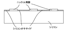
- 1 is a schematic diagram showing a substrate of Example 1.
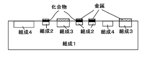
- FIG. 1 (a) is an example of a substrate having regions having different compositions 1 to 4 on the surface
- FIG. 1 (b) is only selective for compositions 2 and 3 as one or more specific compositions.
- 2 is an example of a substrate on which a metal is deposited.
- FIG. 2 and FIG. 3 show an example when the substrate is heat-treated.
- a compound of the metal and an element constituting the substrate surface region portion on which the metal is deposited is formed from the contact surface with the metal.
- the metal on the side away from the contact surface may remain unreacted, and has a metal region portion where a compound of the metal and the element constituting the substrate surface region portion on which the metal is deposited is not formed. May be.
- FIG. 2 shows an example in which, in composition 2, a region formed by forming a compound of a metal and an element constituting composition 2 is a part, and the metal on the side away from the contact surface remains unreacted. Show. 2 and 3, the metal on the composition 3 does not form a compound with the elements constituting the composition 3, but the entire surface or a part of the metal deposits forms a metal compound in all regions where the metal is deposited. You may do it. By selectively leaving unreacted metal, the resistance value in this region can be lowered, so it is preferable to leave unreacted metal.
- FIG. 4 shows that metal is further deposited on the metal selectively deposited initially, the metal deposition portion is extended, and portions of the initially deposited metal regions that are separated from each other are connected by the further deposited metal deposition portion. An example of the case is shown.
- the metal is further deposited before the heat treatment, but the metal may be further deposited after the heat treatment.
- Examples of the base material having a region having a different composition on the surface in the present invention include base materials used for transistors (MOS type transistors), and the surface includes single crystal silicon, polysilicon, compound semiconductor, metal, and metal silicon. And a substrate having a region portion having a composition such as a nitride, a silicon oxide, a nitride, a carbide, or a boride.
- the composition in which metal is selectively deposited is silicon, polysilicon, compound semiconductor, metal, metal silicide, etc.
- the composition in which metal is not deposited is silicon oxide, nitride, carbide, boride.
- Examples of the compound semiconductor include InP, GaAs, GaP, GaN, and InAs.
- Examples of the metal include nickel and cobalt.
- Examples of the metal silicide include nickel silicide and cobalt silicide.
- a substrate having a silicon and silicon oxide region portion on the surface can be obtained by oxidizing a silicon wafer to form a silicon oxide film on the surface and leaving a necessary portion of the silicon oxide film by etching or the like.
- Examples of a method of selectively depositing metal on a region having a specific composition or a plurality of components include, for example, an electroless plating method, sputtering after patterning and protecting with a resist (lift-off), and patterning with resist after sputtering. For example, there is a method of removing unnecessary portions by protecting and etching. Among these methods, it is preferable to selectively deposit metal by electroless plating because it does not involve complicated steps. For example, by performing plating using a specific electroless plating solution on a substrate having at least a silicon and silicon oxide region portion, a metal is not deposited on the silicon oxide region portion, but the silicon region portion is deposited. A metal can be selectively deposited.
- an electroless plating solution for depositing a metal by an electroless plating method on the surface of one or more specific region regions of a substrate having a region portion having a different composition on the surface for example, a fluorine compound
- aqueous solution containing a reducing agent and a metal salt, using ammonia as a pH adjusting agent, and having a pH of 6 or more is preferable.
- ammonium fluoride As the fluorine compound, ammonium fluoride, potassium fluoride, sodium fluoride and the like can be used, but ammonium fluoride is preferable.
- phosphinic acid As the reducing agent, it is preferable to use phosphinic acid because a liquid containing no Na or K can be obtained. Further, dimethylamine borane (DMAB) can also be preferably used. Of course, a salt such as sodium phosphinate can also be used.
- the metal salt examples include salts of cobalt, copper, nickel, alloys thereof, and the like, and nickel salts are preferable.
- the nickel salt a water-soluble nickel salt used in a general electroless nickel plating solution can be used. Examples thereof include nickel sulfate, nickel chloride, nickel hypophosphite, and the like.
- the Si substrate is eroded by about 50 nm and voids are generated.
- the pH is preferably 6 to 10, and more preferably 7 to 9. Thereby, there is little erosion of Si and substitution / reduction plating becomes possible.
- Polycarboxylic acid or a salt thereof can be added to the electroless plating solution of the present invention as necessary.
- the polycarboxylic acid or a salt thereof citric acid or a salt thereof is preferable.
- polycarboxylic acid having a plurality of carboxyl groups in the molecule such as citric acid
- the silicon surface becomes smooth. Since polycarboxylic acid is adsorbed to silicon, the substitution reaction between silicon and metal such as nickel is moderated, so that the substitution reaction does not proceed locally, resulting in a flat silicon-plated film interface. It is considered possible. However, if the amount added is too large, the speed is high and the stability becomes uneasy.
- stabilizers such as tartaric acid, glycine, and malonic acid, reaction accelerators, surfactants, and the like can be contained as required, but it is desirable that they do not contain alkali metals such as sodium and potassium.
- alkali metals such as sodium and potassium.
- those containing alkali metals such as sodium and potassium are not preferable because they cause contamination and cause leakage current and oxide film destruction due to metal contamination.
- phosphinic acid is 0.01 to 1 mol / L, preferably 0.05 to 0.5 mol / L
- fluorine compound is 0.1 to 5 mol / L, preferably 0.5 to 2 mol / L
- metal salt is 0 0.01 to 0.5 mol / L, preferably 0.05 to 0.2 mol / L
- polycarboxylic acid is preferably 0.02 to 1 mol / L, preferably 0.1 to 0.4 mol / L.
- the substrate is degreased with an alkaline aqueous solution having a pH of 12 or more, and then electroless plating is performed using the electroless plating solution.
- the temperature of the plating solution is preferably 50 to 90 ° C, more preferably 60 to 80 ° C.
- the plating time is 0.5 to 5 minutes, preferably 1 to 3 minutes.
- a degreasing treatment with an alkaline aqueous solution.
- an alkaline aqueous solution instead of a hydrofluoric acid-based or manganese-based etchant, the oxide film is not peeled off or damaged, so that it is possible to express good selectivity between silicon oxide and silicon.
- a conventional fluorine-based or manganese-based etchant is used, it is difficult to form a selective plating thin film.
- a phosphoric acid alkaline degreasing agent is preferable.
- alkali metals such as sodium and potassium cause contamination, and the generation of leakage current and destruction of the oxide film due to metal contamination occur. Therefore, it is not preferable to use alkalis containing these alkali metals.
- a cleaner ST manufactured by Nikko Metal Co., Ltd. having a pH of 12.0 to 12.5 in the bath can be preferably used.
- a plated thin film can be selectively formed, and at the same time, the uniformity of the plated film is improved.
- a compound of the metal and an element constituting the substrate surface region portion where the metal is deposited is formed in a part or all of the region where the metal is deposited.
- the temperature may be sufficient. For example, it may be performed at 1000 ° C. for several seconds to several tens of minutes in an inert gas atmosphere, and may be performed at a lower temperature of 300 to 800 ° C. depending on the degree of reaction.
- the composition of the substrate surface region portion that forms a compound with the deposited metal include single crystal silicon, polysilicon, metal, metal silicide, and the like.
- the composition of the substrate surface region is a compound semiconductor
- the resistance value of the gate electrode can be lowered. Therefore, the resistance value of the gate electrode can be adjusted by adjusting the amount of metal left depending on the purpose.
- the electrode may be formed by selectively depositing metal at the same time. Heat treatment is performed to form a compound of the metal and an element constituting the base material surface region where the metal is deposited in a part of the region where the metal is deposited, and leave a part of the metal as an unreacted metal.
- the resistance value of the source / drain electrodes can be lowered. The resistance value is adjusted by adjusting the thickness of the unreacted metal layer and the portion (source / drain junction depth) where the compound of the metal and the element constituting the substrate surface region where the metal is deposited is formed according to the purpose. The resistance can be reduced by increasing the thickness of the unreacted metal layer.
- the metal is further deposited on the substrate surface region where the metal is initially deposited, the metal deposition region is extended, and the surfaces of the substrates on which the metal is initially deposited are separated from each other by the further deposited metal deposition portion.
- Examples of the method include electroless plating. By taking a long electroless plating time and utilizing lateral film growth, it is possible to connect the surfaces of the substrates on which metal is deposited at an early stage apart from each other.
- Examples of the metal that is further deposited by the electroless plating method include the same metals as those selectively deposited at the beginning, that is, cobalt, nickel, copper, or alloys thereof, or those obtained by sequentially stacking each other. .
- Example 1 A silicon oxide (SiO 2 ) film was formed by oxidation with dry oxygen at 1000 ° C. for 1 hour on a silicon wafer adjusted for impurity concentration, etc., and only the necessary portions were left by photoetching, and the others were removed.
- a silicon wafer having a region portion having a composition of silicon and silicon oxide is immersed in a phosphoric acid alkaline degreasing agent (cleaner ST manufactured by Nikko Metal Co., Ltd.) at 60 ° C. for 3 minutes, and electroless nickel plating having the following composition is used. Electroless plating was performed to selectively form a nickel thin film only on silicon.
- a phosphoric acid alkaline degreasing agent cleaning ST manufactured by Nikko Metal Co., Ltd.
- a substrate on which a nickel thin film is selectively formed is shown in FIG.
- the nickel thin film thickness by electroless plating was 80 nm, and the erosion degree of the plating interface was also good.
- heat treatment was performed in an inert gas atmosphere at 400 ° C. for 30 minutes to form a nickel and silicon compound. After the heat treatment, 40 nm was silicided.
- Plating solution composition Nickel sulfate 0.08mol / L Citric acid 0.1 mol / L Ammonium fluoride 0.25 mol / L Phosphinic acid 0.2mol / L pH 8.0 pH adjuster NH 4 OH Bath temperature 70 ° C Immersion time 3 minutes Good degree of erosion at the interface
- Example 2 The same operation as in Example 1 was performed except that the plating time was 1 minute. Similar to Example 1, a nickel thin film was selectively formed only on silicon, and a nickel and silicon compound was formed by heat treatment. The nickel thin film by electroless plating was 60 nm, and the erosion degree of the plating interface was also good.
Landscapes
- Chemical & Material Sciences (AREA)
- General Chemical & Material Sciences (AREA)
- Chemical Kinetics & Catalysis (AREA)
- Engineering & Computer Science (AREA)
- Materials Engineering (AREA)
- Mechanical Engineering (AREA)
- Metallurgy (AREA)
- Organic Chemistry (AREA)
- Inorganic Chemistry (AREA)
- Chemically Coating (AREA)
- Electrodes Of Semiconductors (AREA)
Abstract
本発明は、ゲート電極およびソース・ドレイン領域の抵抗を下げることができ、電流効率を上げることができる基板を提供することを目的とする。さらに、微細化が可能であり、煩雑な工程を必要とせずに製造可能である基板を提供することを目的とする。 表面に周囲とは異なる組成の領域部分を有する基材の、特定の一つまたは複数の該組成の領域部分の表面に選択的に、金属を堆積し、熱処理を施して、金属が堆積した領域部分の一部または全てで当該金属と、金属が堆積した基材表面領域部分を構成する元素との化合物を形成してなる基板であり、金属が堆積した領域部分の一部で当該金属と、金属が堆積した基材表面領域部分を構成する元素との化合物を形成し、かつ堆積させた該金属の一部が未反応の金属として残ってなることが好ましい。
Description
本発明は、トランジスタ等の半導体デバイスに用いる基板に関する。
近年トランジスタ等の半導体デバイスにおいては、微細化が望まれている。
今までは、トランジスタのゲート長を短くしゲート絶縁膜を更に薄くすることにより微細化を図ってきたが、その限界が認識されるようになってきた。その限界を打ち破る技術として、(1)ゲート絶縁膜およびゲート電極向け新材料、(2)電子移動度を高める歪シリコン(ゲルマニウム)、(3)新規構造等が注目されている。
今までは、トランジスタのゲート長を短くしゲート絶縁膜を更に薄くすることにより微細化を図ってきたが、その限界が認識されるようになってきた。その限界を打ち破る技術として、(1)ゲート絶縁膜およびゲート電極向け新材料、(2)電子移動度を高める歪シリコン(ゲルマニウム)、(3)新規構造等が注目されている。
例えば上記(1)に関するゲート周りの新技術では、トランジスタにはソースとドレイン間を流れる電流がゲートに流れ込まないようにゲートの下にゲート絶縁膜と呼ぶ薄膜を形成している。その薄膜が薄いほどトランジスタが高速に動作することになるが、そのかわりゲートリーク電流も増大することになる。近年の微細化に伴いリーク電流の問題は顕著になりつつある。それを防ぐ方法として、(a)High-k材料の採用、(b)メタルゲートの採用、が考えられている。例えば、High-k材料として、二酸化ジルコニウム、酸化ハフニウム、二酸化チタン、五酸化タンタルなどが検討されており、ゲートリーク電流が1/1000に削減されることが確認されている。
一方、メタルゲートに関しては、従来のポリシリコンではなく抵抗が低いニッケルシリサイドやチタンナイトライド、タンタルシリコンナイトライドなどが検討されている。ゲート電極として抵抗が低いメタルゲートを用いることにより、ゲート抵抗とソース・ドレイン間の抵抗を低減できることになる。更に高機能化を図るためには、薄膜化が望まれている。
一方、ソース・ドレインはショートチャネル効果抑制のため接合深さを浅くすることが推進され、接合深さを浅くすることによる抵抗値の増大が問題となっている。抵抗の増大は駆動電流を低下させる。このためソース・ドレインの抵抗を下げる必要がある。従来技術では、ソース・ドレインの抵抗を下げるため、高融点金属を堆積し、熱処理でシリサイドを形成するが、Siを消費するためソース・ドレイン接合深さ以上に厚いシリサイドを形成できない。
また、従来トランジスタの製造プロセスにおいて、スパッタリングとエッチングを駆使して必要部に金属薄膜を形成するという方法が取られてきた。
いくつかの異なる組成領域部分から構成される基板の表面、例えばシリコンとシリコンオキサイドから構成される基板の表面の一部にシリサイドを形成する場合、従来はスパッタリング法などにより全面に金属を堆積して熱処理を施し、シリコンに接する領域部分のみシリサイド化し、未反応の金属を除去することにより、基板表面の一部を選択的にシリサイド化する工程がとられていた。しかし、この場合は、未反応の金属は除去せざるを得ず、選択的に残すことができず、シリサイド部を含む領域部分の抵抗値がシリサイド化した領域部分の抵抗値で決まる。このシリサイド化した領域部分をゲート電極とする場合、その抵抗値は低いことが望まれる。シリサイド化した領域部分を厚くすると抵抗値が下がるが、薄膜化が望まれ、それ以上抵抗値を下げることができなかった。また、このシリサイド化した領域部分をソース・ドレイン領域とする場合、ソース・ドレイン領域は接合深さが浅く、抵抗値が低いことが望まれる。接合深さより深くシリサイド層を形成するわけにはいかないため、ソース・ドレインの抵抗値をそれ以上下げることができなかった。
いくつかの異なる組成領域部分から構成される基板の表面、例えばシリコンとシリコンオキサイドから構成される基板の表面の一部にシリサイドを形成する場合、従来はスパッタリング法などにより全面に金属を堆積して熱処理を施し、シリコンに接する領域部分のみシリサイド化し、未反応の金属を除去することにより、基板表面の一部を選択的にシリサイド化する工程がとられていた。しかし、この場合は、未反応の金属は除去せざるを得ず、選択的に残すことができず、シリサイド部を含む領域部分の抵抗値がシリサイド化した領域部分の抵抗値で決まる。このシリサイド化した領域部分をゲート電極とする場合、その抵抗値は低いことが望まれる。シリサイド化した領域部分を厚くすると抵抗値が下がるが、薄膜化が望まれ、それ以上抵抗値を下げることができなかった。また、このシリサイド化した領域部分をソース・ドレイン領域とする場合、ソース・ドレイン領域は接合深さが浅く、抵抗値が低いことが望まれる。接合深さより深くシリサイド層を形成するわけにはいかないため、ソース・ドレインの抵抗値をそれ以上下げることができなかった。
このような問題点に対し、例えば特許文献1(米国特許出願公開第2005/0212058号明細書)では、ゲート電極とソース・ドレイン領域を有するシリコン基板にスパッタリング等の物理的気相成長法(PVD)法により一面に金属薄膜を形成し、熱処理によりシリコンに接する領域部分のみをシリサイド化し、未反応の金属薄膜を除去した後に、無電解めっきによりゲート電極とソース・ドレイン領域上に金属膜を形成し、ゲート電極、ソース・ドレイン領域の抵抗値を下げる方法が開示されている。この方法では、PVD法により金属薄膜を形成していることから、選択性がなく、従ってシリサイド化後に不要な部分の金属薄膜を剥離することが必要である。また、その剥離工程で必要な部分の金属薄膜も剥離してしまうことになり、結果的に電極部のシリサイドした膜と金属膜の共存が不可能になっていた。
また、近年、基板上に形成する金属薄膜を無電解めっきにて形成することが検討されている。
特許文献2(特開平2-63129号公報)には、無電解めっきによるゲート電極の形成方法について開示されているが、ゲート電極の断面を増大させて電界効果トランジスタのゲート抵抗の低下を防ぐためゲート電極の形状をマッシュルーム型にしたことを特徴とするもので、めっきをしたくない場所にはレジストを使用している。
特許文献2(特開平2-63129号公報)には、無電解めっきによるゲート電極の形成方法について開示されているが、ゲート電極の断面を増大させて電界効果トランジスタのゲート抵抗の低下を防ぐためゲート電極の形状をマッシュルーム型にしたことを特徴とするもので、めっきをしたくない場所にはレジストを使用している。
特許文献3(特開平3-155629号公報)には、集積回路の電極形成に無電解ニッケルめっきを用いることが開示されている。シリコンウェハー上に酸化シリコン膜を形成し、フォトリソグラフを用いて下地チタン膜を露出させ、塩化パラジウム水溶液によるチタン膜表面への触媒付与により1μm厚の無電解ニッケルめっき膜を形成することにより電極を形成する方法が開示されている。無電解ニッケルめっきを開始する触媒として塩化パラジウムを必要とし、形成した電極の膜厚が1μmと厚い。
特許文献4(特開2005-336600号公報)では、シリコン基板上にめっきをするために、フッ酸、フッ化アンモニウムと無電解めっき用触媒金属となるパラジウム化合物を含む水溶液に浸漬して触媒化後、無電解ニッケルめっきを行っており、触媒の付与が必要である。また、めっき選択性の発現が困難である。
シリコンと酸化シリコン上のめっきの選択性については、非特許文献1(丹羽大介(Daisuke Niwa)他、エレクトロキミカ・アクタ(Electrochimica Acta) 48(2003)、p.1295-1300)にSi上への選択無電解ニッケルめっきについて紹介している。1段目の核形成段階としては、還元剤が入っていないNi塩水溶液を使用し、2段目の成膜工程においては、還元剤が入った水溶液を使用している。この方法によると、SiとSiO2の共存する基板において、Si上に選択的にニッケル膜を形成できることが示されている。
また、特許文献5(特許第3235583号公報)においても表面にシリコンの領域と酸化シリコンの領域を有するシリコン基板のシリコン上に無電解めっきにより選択的に金属膜を形成し、加熱処理しシリサイド化する半導体の製造方法が記載されている。シリサイド化する金属膜中にあらかじめ下地のシリコンにイオン注入した元素と同種の導電機構を有する不純物を含有させることにより、高い不純物濃度を有する微細なパターンにおいて、シリサイドを自己整合的に形成した後でもゲートや拡散層の抵抗を低減できるとしている。特許文献5では無電解めっきにより選択的に金属膜を形成できるとしているが、実際にはこの方法では無電解めっきにより選択的に金属膜を形成するのは困難である。即ち、無電解めっきにより選択的に金属膜を形成するために、シリコン上に選択的にPd等の触媒を付与するとしているが、Pd吸着に選択性の問題があり、実際にPdを選択的に付着させるには非選択部分の保護など、何らかの手段が必要となり、煩雑な工程が必要となる。事実、前記特許文献5においても、非選択成長となった金属めっき膜は熱処理を行った後にウェットエッチングすることにより除去することが教示されている。
丹羽大介(Daisuke Niwa)他、エレクトロキミカ・アクタ(Electrochimica Acta) 48(2003)、p.1295-1300
本発明は、ゲート電極およびソース・ドレイン領域の抵抗を下げることができ、電流効率を上げることができる基板を提供することを目的とする。
さらに、微細化が可能であり、煩雑な工程を必要とせずに製造可能である基板を提供することを目的とする。
さらに、微細化が可能であり、煩雑な工程を必要とせずに製造可能である基板を提供することを目的とする。
本発明者らはかかる状況を鑑み、被めっき材の材質により選択性を発現できる無電解めっき法に着目し、表面に異なる組成の領域部分を有する基材において、特定の一つまたは複数の組成の領域部分の表面に、当該表面を大きく粗すことなく選択的に金属を堆積し、熱処理を施して、金属が堆積した領域部分の一部または全てで当該金属と、金属が堆積した基材表面領域部分を構成する元素との化合物を形成してなる基板とすることにより、煩雑な工程を必要とせず、微細化が可能であり、このような基板を用いることにより、トランジスタにおいてゲート電極およびソース・ドレイン領域の抵抗を下げることができることを見出し本発明に至った。
即ち、本発明は以下のとおりである。
即ち、本発明は以下のとおりである。
(1)表面に周囲とは異なる組成の領域部分を有する基材の、特定の一つまたは複数の該組成の領域部分の表面に選択的に、金属を堆積し、熱処理を施して、金属が堆積した領域部分の一部または全てで当該金属と、金属が堆積した基材表面領域部分を構成する元素との化合物を形成してなる基板。
(2)前記基板が、金属が堆積した領域部分の一部で当該金属と、金属が堆積した基材表面領域部分を構成する元素との化合物を形成し、かつ堆積させた該金属の一部が未反応の金属として残ってなる前記(1)記載の基板。
(2)前記基板が、金属が堆積した領域部分の一部で当該金属と、金属が堆積した基材表面領域部分を構成する元素との化合物を形成し、かつ堆積させた該金属の一部が未反応の金属として残ってなる前記(1)記載の基板。
(3)前記基板にさらに金属を堆積して、初期に選択的に金属を堆積した基板表面領域部分の範囲を超えて、金属堆積部を延伸させることにより、互いに離れた初期に金属を堆積した基板表面領域部分どうしをさらに堆積した金属堆積部で接続させてなる前記(1)または(2)に記載の基板。
(4)前記選択的に金属が堆積する基材表面領域部分の組成が、単結晶シリコン、ポリシリコン、化合物半導体、金属、金属のケイ化物のいずれかである前記(1)~(3)のいずれかに記載の基板。
(5)前記選択的に金属が堆積しない基材表面領域部分の組成が、ケイ素の酸化物、窒化物、炭化物、ホウ化物のいずれかである前記(1)~(4)のいずれかに記載の基板。
(6)前記初期に選択的に堆積する金属、及びさらに延伸させるために堆積する金属が、Co、Ni、Cu、またはそれらの合金、もしくはそれぞれを順に重ねて堆積したものである前記(1)~(5)のいずれかに記載の基板。
(5)前記選択的に金属が堆積しない基材表面領域部分の組成が、ケイ素の酸化物、窒化物、炭化物、ホウ化物のいずれかである前記(1)~(4)のいずれかに記載の基板。
(6)前記初期に選択的に堆積する金属、及びさらに延伸させるために堆積する金属が、Co、Ni、Cu、またはそれらの合金、もしくはそれぞれを順に重ねて堆積したものである前記(1)~(5)のいずれかに記載の基板。
(7)前記選択的に堆積する金属が無電解めっきにより堆積されてなる前記(1)~(6)のいずれかに記載の基板。
(8)前記無電解めっきが、フッ素化合物、還元剤、及び金属塩を含有し、pH調整剤としてアンモニアを用い、pH6以上としてなる無電解めっき液を用いてなる前記(7)記載の基板。
(8)前記無電解めっきが、フッ素化合物、還元剤、及び金属塩を含有し、pH調整剤としてアンモニアを用い、pH6以上としてなる無電解めっき液を用いてなる前記(7)記載の基板。
(9)前記無電解めっき液が、さらにポリカルボン酸またはその塩を含有させてなる前記(8)記載の基板。
(10)前記ポリカルボン酸またはその塩が、クエン酸またはその塩である前記(9)記載の基板。
(10)前記ポリカルボン酸またはその塩が、クエン酸またはその塩である前記(9)記載の基板。
(11)前記フッ素化合物が、フッ化アンモニウムである前記(8)~(10)のいずれかに記載の基板。
(12)前記無電解めっき液が、アルカリ金属を含有しない前記(8)~(11)のいずれかに記載の基板。
(12)前記無電解めっき液が、アルカリ金属を含有しない前記(8)~(11)のいずれかに記載の基板。
(13)前記無電解めっき液の金属塩の金属がNiである前記(8)~(12)のいずれかに記載の基板。
(14)前記無電解めっき液で金属が堆積する基材表面領域部分が単結晶シリコンまたはポリシリコンである前記(8)~(13)のいずれかに記載の基板。
(15)前記無電解めっき液で堆積させた金属の厚みが200nm以下である前記(8)~(14)のいずれかに記載の基板。
(14)前記無電解めっき液で金属が堆積する基材表面領域部分が単結晶シリコンまたはポリシリコンである前記(8)~(13)のいずれかに記載の基板。
(15)前記無電解めっき液で堆積させた金属の厚みが200nm以下である前記(8)~(14)のいずれかに記載の基板。
(16)前記基板が、特定の一つまたは複数の組成の領域部分の表面に選択的に、金属を堆積する前に、アルカリ性水溶液で前処理されてなる前記(1)~(15)のいずれかに記載の基板。
(17)前記(2)~(16)のいずれかに記載の基板を用い、選択的に堆積させた金属の一部が未反応の金属として残してなる部分を電極として備えることを特徴とする半導体素子。
本発明によれば、表面に周囲とは異なる組成の領域部分を有する基材表面の、特定の一つまたは複数の該組成の領域部分の表面に選択的に、金属を堆積し、熱処理を施して、金属が堆積した領域部分の一部で当該金属と、金属が堆積した基材表面領域部分を構成する元素との化合物を形成し、堆積させた該金属の一部を未反応の金属として残した基板は、トランジスタ等の半導体素子に用いた場合、堆積させた該金属の一部を未反応の金属として残した部分を電極とすることにより、ゲート電極およびソース・ドレイン領域の抵抗値を下げることができ、電流効率を上げることが可能な基板となる。
特にトランジスタの電極作製において、シリコンとシリコンオキサイドが共存する状態で、特定の無電解ニッケルめっき液を用いると、シリコン上に選択的にニッケル薄膜を形成できる。また、めっき膜と被めっき物の界面も平坦であり、密着性も良好である。
無電解めっきにより、シリコンとシリコンオキサイドが共存する状態で、シリコン上に選択的にニッケル薄膜形成できることにより、従来の選択性のないスパッタ法と比較して成膜後の不要部の剥離工程を必要としないことから、プロセス上のメリットが大きい。
また、ソース・ドレイン接合深さと未反応の金属層の厚さを調整することにより、抵抗値を調整することができ、未反応の金属層の厚さを厚くすることにより低抵抗化できる。
無電解めっきにより、シリコンとシリコンオキサイドが共存する状態で、シリコン上に選択的にニッケル薄膜形成できることにより、従来の選択性のないスパッタ法と比較して成膜後の不要部の剥離工程を必要としないことから、プロセス上のメリットが大きい。
また、ソース・ドレイン接合深さと未反応の金属層の厚さを調整することにより、抵抗値を調整することができ、未反応の金属層の厚さを厚くすることにより低抵抗化できる。
本発明の、表面に周囲とは異なる組成の領域部分を有する基材表面の、特定の一つまたは複数の組成の領域部分の表面に選択的に、金属を堆積してなる基板を図面を用いて模式的に説明する。
図1(a)は、表面に異なる組成1~4の領域部分を有する基材の一例であり、図1(b)は、特定の一つまたは複数の組成として組成2、3にのみ選択的に金属を堆積させた基板の一例である。
図1(a)は、表面に異なる組成1~4の領域部分を有する基材の一例であり、図1(b)は、特定の一つまたは複数の組成として組成2、3にのみ選択的に金属を堆積させた基板の一例である。
図2及び図3に、この基板に熱処理を施した場合の一例を示す。前記金属が堆積した基板を熱処理することにより、金属との接触面から、金属と金属が堆積した基材表面領域部分を構成する元素との化合物が形成される。この際、接触面から離れた側の金属は未反応で残っても良く、また、金属と金属が堆積した基材表面領域部分を構成する元素との化合物が形成されない金属領域部分を有していても良い。
図2においては、組成2上に堆積した金属が全てが、組成2の領域部分を構成する元素との化合物を形成してなる。また、組成2において、金属と、組成2を構成する元素との化合物を形成してなる領域が一部であり、接触面から離れた側の金属が未反応で残っている例を図3に示す。図2、図3においては、組成3上の金属は、組成3を構成する元素との化合物を形成していないが、金属が堆積した全ての領域部分で、全面又は一部が金属化合物を形成していても良い。未反応の金属を選択的に残すことにより、この領域部分の抵抗値を下げることができるので、未反応の金属を残すことが好ましい。
図4は初期に選択的に堆積した金属の上にさらに金属を堆積させ、金属堆積部を延長させ、互いに離れた初期に堆積した金属領域部分どうしを、さらに堆積した金属堆積部で接続させた場合の一例を示したものである。
図4においては、熱処理を施す前にさらに金属を堆積しているが、さらに金属を堆積させるのは、熱処理を施した後でもよい。
図4においては、熱処理を施す前にさらに金属を堆積しているが、さらに金属を堆積させるのは、熱処理を施した後でもよい。
本発明における表面に異なる組成の領域部分を有する基材としては、例えば、トランジスタ(MOS型トランジスタ)に用いる基材が挙げられ、表面に単結晶シリコン、ポリシリコン、化合物半導体、金属、金属のケイ化物、ケイ素の酸化物、窒化物、炭化物、ホウ化物等の組成の領域部分を有する基材が挙げられる。このうち金属が選択的に堆積する組成としては、シリコン、ポリシリコン、化合物半導体、金属、金属のケイ化物等であり、金属が堆積しない組成としてはケイ素の酸化物、窒化物、炭化物、ホウ化物であることが好ましい。上記化合物半導体としては、InP、GaAs、GaP、GaN、InAs等が挙げられ、金属としてはニッケル、コバルト等が挙げられ、金属のケイ化物としては、ニッケルシリサイド、コバルトシリサイド等が挙げられる。
例えば、表面にシリコンとシリコンオキサイドの領域部分を有する基材は、シリコンウェハーを酸化して表面にシリコンオキサイド膜を形成し、エッチング等によりシリコンオキサイド膜の必要部を残すことにより得ることができる。
例えば、表面にシリコンとシリコンオキサイドの領域部分を有する基材は、シリコンウェハーを酸化して表面にシリコンオキサイド膜を形成し、エッチング等によりシリコンオキサイド膜の必要部を残すことにより得ることができる。
特定の一つまたは複数の組成の領域部分に選択的に金属を堆積させる方法としては、例えば、無電解めっき方法、レジストでパターニングし保護した後スパッタリングしたり(リフトオフ)、スパッタリングした後レジストでパターニングし保護してエッチングして不要部分を削除したりする方法等が挙げられる。
これらの方法の中で、無電解めっきにより選択的に金属を堆積させることが煩雑な工程を含まないので好ましい。例えば、少なくともシリコンとシリコンオキサイドの領域部分を有する基材に、特定の無電解めっき液を用いてめっきを行うことにより、シリコンオキサイドの領域部分には金属を堆積させずに、シリコンの領域部分に選択的に金属を堆積させることができる。
これらの方法の中で、無電解めっきにより選択的に金属を堆積させることが煩雑な工程を含まないので好ましい。例えば、少なくともシリコンとシリコンオキサイドの領域部分を有する基材に、特定の無電解めっき液を用いてめっきを行うことにより、シリコンオキサイドの領域部分には金属を堆積させずに、シリコンの領域部分に選択的に金属を堆積させることができる。
上記表面に異なる組成の領域部分を有する基材の特定の一つまたは複数の組成の領域部分の表面に、無電解めっき方法で金属を堆積させる際の無電解めっき液としては、例えば、フッ素化合物、還元剤、及び金属塩を含有し、pH調整剤としてアンモニアを用い、pH6以上とした水溶液が好ましい。
フッ素化合物としては、フッ化アンモニウム、フッ化カリウム、フッ化ナトリウム等を用いることができるが、フッ化アンモニウムが好ましい。
還元剤としては、ホスフィン酸を用いることにより、Na、Kを含まない液とすることができるので好ましい。また、ジメチルアミンボラン(DMAB)も好ましく用いることができる。もちろんホスフィン酸ナトリウムなどの塩も用いることができる。
還元剤としては、ホスフィン酸を用いることにより、Na、Kを含まない液とすることができるので好ましい。また、ジメチルアミンボラン(DMAB)も好ましく用いることができる。もちろんホスフィン酸ナトリウムなどの塩も用いることができる。
金属塩としては、コバルト、銅、ニッケル、それらの合金等の塩が挙げられ、ニッケル塩が好ましい。ニッケル塩としては、一般的な無電解ニッケルめっき液に使用される水溶性ニッケル塩を使用することができる。例えば硫酸ニッケル、塩化ニッケル、次亜リン酸ニッケル、などが挙げられる。
Si上ではめっき時に交換反応が生じるとSi基板が50nm程度侵食され、ボイドが発生する。このめっき時に侵食におけるボイド発生がなく界面を平坦とするためにはアンモニアによりpH6以上に調整すること、及びフッ素化合物の共存が必要となる。pHは6~10が好ましく、7~9がより好ましい。これによりSiの侵食が少なく、置換・還元めっきが可能となる。
Si上ではめっき時に交換反応が生じるとSi基板が50nm程度侵食され、ボイドが発生する。このめっき時に侵食におけるボイド発生がなく界面を平坦とするためにはアンモニアによりpH6以上に調整すること、及びフッ素化合物の共存が必要となる。pHは6~10が好ましく、7~9がより好ましい。これによりSiの侵食が少なく、置換・還元めっきが可能となる。
本発明の無電解めっき液には、必要に応じてポリカルボン酸またはその塩を加えることができる。ポリカルボン酸またはその塩としては、クエン酸またはその塩が好ましい。クエン酸等の分子内に複数個のカルボキシル基を有するポリカルボン酸を加えることによりシリコン面が平滑となる。ポリカルボン酸は、シリコンに吸着するためシリコンとニッケル等の金属の置換反応を温和にするために、局部的に置換反応が進まず、結果的に平坦なシリコンとめっき膜の界面にすることができると考えられる。ただし、添加量が多すぎると速度が速く安定性が不安となる。
その他必要に応じて酒石酸、グリシン、マロン酸等の安定剤、反応促進剤、界面活性剤などを含有することができるが、ナトリウムやカリウムなどのアルカリ金属を含んでいないことが望ましい。半導体デバイスではナトリウムやカリウムなどのアルカリ金属を含むものは汚染の原因となり、リーク電流の発生や金属汚染による酸化膜破壊が生じるので好ましくない。
これらのめっき浴の成分は、通常用いられている濃度の範囲で用いることができる。例えば、ホスフィン酸は0.01~1mol/L、好ましくは0.05~0.5mol/L、フッ素化合物は0.1~5mol/L、好ましくは0.5~2mol/L、金属塩は0.01~0.5mol/L、好ましくは0.05~0.2mol/L、ポリカルボン酸は0.02~1mol/L、好ましくは0.1~0.4mol/L含有することが好ましい。
めっき方法としては、前記基材を、前処理として、pH12以上のアルカリ水溶液により脱脂処理を行った後、上記無電解めっき液を用いて無電解めっきを行う。このときめっき液の温度は50~90℃が好ましく、60~80℃がより好ましい。また、めっき時間は0.5~5分、好ましくは1~3分である。
本発明のめっき方法により、シリコン上に200nm以下の薄膜を形成することができる。さらには100nm以下の薄膜とすることもでき、微細化が可能である。
本発明のめっき方法により、シリコン上に200nm以下の薄膜を形成することができる。さらには100nm以下の薄膜とすることもでき、微細化が可能である。
前処理としては、アルカリ水溶液により脱脂処理を行うことが好ましい。フッ酸系やマンガン系のエッチャントではなくアルカリ水溶液を用いることにより、酸化膜の剥離や損傷を与えることがないため良好なシリコンオキサイドとシリコンの選択性を発現することが可能となる。従来のフッ素系やマンガン系のエッチャントを用いると、選択的めっき薄膜を形成することが難しい。脱脂処理に用いるアルカリ水溶液としては、リン酸系のアルカリ脱脂剤が好ましい。半導体デバイスではナトリウムやカリウムなどのアルカリ金属を含むものは汚染の原因となり、リーク電流の発生や金属汚染による酸化膜破壊が生じるのでこれらのアルカリ金属を含むアルカリを用いるのは好ましくない。リン酸系のアルカリ脱脂剤としては、例えば建浴でpH12.0~12.5である日鉱金属株式会社製クリーナーSTを好ましく用いることができる。
また、基材を予めアルカリ水溶液で前処理することにより、選択的にめっき薄膜を形成することができると同時に、めっき膜の均一性が良好となる。
また、基材を予めアルカリ水溶液で前処理することにより、選択的にめっき薄膜を形成することができると同時に、めっき膜の均一性が良好となる。
無電解めっきによる選択性の発現は、従来の選択性がないスパッタ法と比較して成膜後の不要部の剥離工程を必要としないことから、プロセス上のメリットは大きい。
選択的に金属を堆積させた後に行う、熱処理としては、金属が堆積した領域部分の一部又は全てで当該金属と、金属が堆積した基材表面領域部分を構成する元素との化合物を形成する温度でよく、例えば、不活性ガス雰囲気中、1000℃で数秒から数十分間行えばよく、反応の程度により、より低温の300~800℃で行ってもよい。
堆積した金属との化合物を形成する基材表面領域部分の組成としては、単結晶シリコン、ポリシリコン、金属、金属のケイ化物等が挙げられる。また、基材表面領域部分の組成が、化合物半導体の場合は、金属との化合物を形成しにくく、金属は未反応で残る。堆積させた金属の一部を未反応の金属として残した部分をトランジスタのゲート電極として用いることにより、ゲート電極の抵抗値を下げることができる。従って、目的によって残す金属の量を調整することにより、ゲート電極の抵抗値を調整することができる。
堆積した金属との化合物を形成する基材表面領域部分の組成としては、単結晶シリコン、ポリシリコン、金属、金属のケイ化物等が挙げられる。また、基材表面領域部分の組成が、化合物半導体の場合は、金属との化合物を形成しにくく、金属は未反応で残る。堆積させた金属の一部を未反応の金属として残した部分をトランジスタのゲート電極として用いることにより、ゲート電極の抵抗値を下げることができる。従って、目的によって残す金属の量を調整することにより、ゲート電極の抵抗値を調整することができる。
ソース電極やドレイン電極がゲート電極と同じ素材を使用している時は、同時に選択的に金属を堆積させ、電極を形成しても構わない。熱処理をして、金属が堆積した領域部分の一部で該金属と、金属が堆積した基材表面領域部分を構成する元素との化合物を形成し金属の一部を未反応の金属として残すことにより、ソース・ドレイン電極の抵抗値を下げることができる。目的によって前記金属と金属が堆積した基材表面領域部分を構成する元素との化合物を形成した部分(ソース・ドレイン接合深さ)と未反応の金属層の厚さを調整することにより、抵抗値を調整することができ、未反応の金属層の厚さを厚くすることにより低抵抗化できる。
前記初期に金属を堆積した基板表面領域部分に、更に金属を堆積させ、金属堆積領域部分を延伸させ、互いに離れた初期に金属を堆積した基板の表面どうしを、更に堆積した金属堆積部で接続させる方法としては、無電解めっき方法が挙げられる。無電解めっきの時間を長くとり、側方への膜成長を利用することにより、互いに離れた初期に金属を堆積した基板の表面どうしを接続することができる。無電解めっき方法により更に堆積する金属としては、初期に選択的に堆積する金属と同様な金属、即ち、コバルト、ニッケル、銅、またはそれらの合金、もしくはそれぞれを順に重ねて堆積したものが挙げられる。
以下、実施例に基づき本発明を詳述する。
実施例1
不純物濃度調整等をしたシリコンウェハー上に1000℃で1時間乾燥酸素により酸化してシリコンオキサイド(SiO2)膜を形成し、フォトエッチングにより必要部のみを残し、それ以外は除去した。シリコンとシリコンオキサイドの組成の領域部分を有するシリコンウェハーを、リン酸系のアルカリ脱脂剤(日鉱金属株式会社製クリーナーST)に60℃で3分間浸漬し、下記組成の無電解ニッケルめっきを用いて無電解めっきを行い、シリコン上にのみ選択的にニッケル薄膜を形成した。選択的にニッケル薄膜を形成した基板を図5に示す。無電解めっきによるニッケル薄膜厚は80nmであり、めっき界面の侵食度も良好であった。次に400℃で30分間不活性ガス雰囲気中で熱処理を施してニッケルとシリコンの化合物を形成した。熱処理後、40nmがシリサイド化していた。
めっき液組成
硫酸ニッケル 0.08mol/L
クエン酸 0.1mol/L
フッ化アンモニウム 0.25mol/L
ホスフィン酸 0.2mol/L
pH 8.0
pH調整剤 NH4OH
浴温度 70℃
浸漬時間 3分間
界面の侵食度 良好
実施例1
不純物濃度調整等をしたシリコンウェハー上に1000℃で1時間乾燥酸素により酸化してシリコンオキサイド(SiO2)膜を形成し、フォトエッチングにより必要部のみを残し、それ以外は除去した。シリコンとシリコンオキサイドの組成の領域部分を有するシリコンウェハーを、リン酸系のアルカリ脱脂剤(日鉱金属株式会社製クリーナーST)に60℃で3分間浸漬し、下記組成の無電解ニッケルめっきを用いて無電解めっきを行い、シリコン上にのみ選択的にニッケル薄膜を形成した。選択的にニッケル薄膜を形成した基板を図5に示す。無電解めっきによるニッケル薄膜厚は80nmであり、めっき界面の侵食度も良好であった。次に400℃で30分間不活性ガス雰囲気中で熱処理を施してニッケルとシリコンの化合物を形成した。熱処理後、40nmがシリサイド化していた。
めっき液組成
硫酸ニッケル 0.08mol/L
クエン酸 0.1mol/L
フッ化アンモニウム 0.25mol/L
ホスフィン酸 0.2mol/L
pH 8.0
pH調整剤 NH4OH
浴温度 70℃
浸漬時間 3分間
界面の侵食度 良好
実施例2
めっき時間を1分間とした以外は、実施例1と同様の操作を行った。実施例1と同様にシリコン上にのみ選択的にニッケル薄膜が形成され、熱処理によりニッケルとシリコンの化合物が形成された。無電解めっきによるニッケル薄膜は、60nmであり、めっき界面の侵食度も良好であった。
めっき時間を1分間とした以外は、実施例1と同様の操作を行った。実施例1と同様にシリコン上にのみ選択的にニッケル薄膜が形成され、熱処理によりニッケルとシリコンの化合物が形成された。無電解めっきによるニッケル薄膜は、60nmであり、めっき界面の侵食度も良好であった。
Claims (17)
- 表面に周囲とは異なる組成の領域部分を有する基材の、特定の一つまたは複数の該組成の領域部分の表面に選択的に、金属を堆積し、熱処理を施して、金属が堆積した領域部分の一部または全てで当該金属と、金属が堆積した基材表面領域部分を構成する元素との化合物を形成してなる基板。
- 前記基板が、金属が堆積した領域部分の一部で当該金属と、金属が堆積した基材表面領域部分を構成する元素との化合物を形成し、かつ堆積させた該金属の一部が未反応の金属として残ってなる請求項1記載の基板。
- 前記基板にさらに金属を堆積して、初期に選択的に金属を堆積した基板表面領域部分の範囲を超えて、金属堆積部を延伸させることにより、互いに離れた初期に金属を堆積した基板表面領域部分どうしをさらに堆積した金属堆積部で接続させてなる請求項1又は2に記載の基板。
- 前記選択的に金属が堆積する基材表面領域部分の組成が、単結晶シリコン、ポリシリコン、化合物半導体、金属、金属のケイ化物のいずれかである請求項1~3のいずれかに記載の基板。
- 前記選択的に金属が堆積しない基材表面領域部分の組成が、ケイ素の酸化物、窒化物、炭化物、ホウ化物のいずれかである請求項1~4のいずれかに記載の基板。
- 前記初期に選択的に堆積する金属、及びさらに延伸させるために堆積する金属が、Co、Ni、Cu、またはそれらの合金、もしくはそれぞれを順に重ねて堆積したものである請求項1~5のいずれかに記載の基板。
- 前記選択的に堆積する金属が無電解めっきにより堆積されてなる請求項1~6のいずれかに記載の基板。
- 前記無電解めっきが、フッ素化合物、還元剤、及び金属塩を含有し、pH調整剤としてアンモニアを用い、pH6以上としてなる無電解めっき液を用いてなる請求項7記載の基板。
- 前記無電解めっき液が、さらにポリカルボン酸またはその塩を含有させてなる請求項8記載の基板。
- 前記ポリカルボン酸またはその塩がクエン酸またはその塩である請求項9記載の基板。
- 前記フッ素化合物が、フッ化アンモニウムである請求項8~10のいずれかに記載の基板。
- 前記無電解めっき液が、アルカリ金属を含有しない請求項8~11のいずれかに記載の基板。
- 前記無電解めっき液の金属塩の金属がNiである請求項8~12のいずれかに記載の基板。
- 前記無電解めっき液で金属が堆積する基材表面領域部分が単結晶シリコンまたはポリシリコンである請求項8~13のいずれかに記載の基板。
- 前記無電解めっき液で堆積させた金属の厚みが200nm以下である請求項8~14のいずれかに記載の基板。
- 前記基板が、特定の一つまたは複数の組成の領域部分の表面に選択的に、金属を堆積する前に、アルカリ水溶液で前処理されてなる請求項1~15のいずれかに記載の基板。
- 請求項2~16のいずれかに記載の基板を用い、選択的に堆積させた金属の一部が未反応の金属として残してなる部分を電極として備えることを特徴とする半導体素子。
Priority Applications (1)
| Application Number | Priority Date | Filing Date | Title |
|---|---|---|---|
| JP2010511976A JPWO2009139366A1 (ja) | 2008-05-15 | 2009-05-12 | 基板 |
Applications Claiming Priority (2)
| Application Number | Priority Date | Filing Date | Title |
|---|---|---|---|
| JP2008-127836 | 2008-05-15 | ||
| JP2008127836 | 2008-05-15 |
Publications (1)
| Publication Number | Publication Date |
|---|---|
| WO2009139366A1 true WO2009139366A1 (ja) | 2009-11-19 |
Family
ID=41318733
Family Applications (1)
| Application Number | Title | Priority Date | Filing Date |
|---|---|---|---|
| PCT/JP2009/058811 Ceased WO2009139366A1 (ja) | 2008-05-15 | 2009-05-12 | 基板 |
Country Status (3)
| Country | Link |
|---|---|
| JP (1) | JPWO2009139366A1 (ja) |
| TW (1) | TW201001648A (ja) |
| WO (1) | WO2009139366A1 (ja) |
Cited By (2)
| Publication number | Priority date | Publication date | Assignee | Title |
|---|---|---|---|---|
| JP2016510090A (ja) * | 2013-02-22 | 2016-04-04 | アルスィメール | 金イオン及びフッ素イオンを含有する溶液を用いた金属ケイ化物の形成方法 |
| JP2024061524A (ja) * | 2022-10-21 | 2024-05-07 | 関東化学株式会社 | 無電解めっき液組成物および貴金属の析出方法 |
Citations (5)
| Publication number | Priority date | Publication date | Assignee | Title |
|---|---|---|---|---|
| JPS5124176A (en) * | 1974-08-21 | 1976-02-26 | New Nippon Electric Co | Handotaisochino denkyokukeiseiho |
| JPH04180573A (ja) * | 1990-11-14 | 1992-06-26 | Nippon Hyomen Kagaku Kk | 樹脂成形型磁石へのNiめっき方法とNiめっき浴 |
| JP2003073843A (ja) * | 2001-08-28 | 2003-03-12 | Hiroshima Pref Gov | マグネシウム合金素材の無電解ニッケルめっき方法 |
| JP2005336600A (ja) * | 2004-04-30 | 2005-12-08 | Alps Electric Co Ltd | シリコン基板の無電解めっき方法およびシリコン基板上の金属層形成方法 |
| WO2006065221A1 (en) * | 2004-12-14 | 2006-06-22 | Polymer Kompositer I Göteborg Ab | Stabilization amd performance of autocatalytic electroless processes. |
-
2009
- 2009-05-12 JP JP2010511976A patent/JPWO2009139366A1/ja not_active Withdrawn
- 2009-05-12 WO PCT/JP2009/058811 patent/WO2009139366A1/ja not_active Ceased
- 2009-05-13 TW TW098115780A patent/TW201001648A/zh unknown
Patent Citations (5)
| Publication number | Priority date | Publication date | Assignee | Title |
|---|---|---|---|---|
| JPS5124176A (en) * | 1974-08-21 | 1976-02-26 | New Nippon Electric Co | Handotaisochino denkyokukeiseiho |
| JPH04180573A (ja) * | 1990-11-14 | 1992-06-26 | Nippon Hyomen Kagaku Kk | 樹脂成形型磁石へのNiめっき方法とNiめっき浴 |
| JP2003073843A (ja) * | 2001-08-28 | 2003-03-12 | Hiroshima Pref Gov | マグネシウム合金素材の無電解ニッケルめっき方法 |
| JP2005336600A (ja) * | 2004-04-30 | 2005-12-08 | Alps Electric Co Ltd | シリコン基板の無電解めっき方法およびシリコン基板上の金属層形成方法 |
| WO2006065221A1 (en) * | 2004-12-14 | 2006-06-22 | Polymer Kompositer I Göteborg Ab | Stabilization amd performance of autocatalytic electroless processes. |
Cited By (2)
| Publication number | Priority date | Publication date | Assignee | Title |
|---|---|---|---|---|
| JP2016510090A (ja) * | 2013-02-22 | 2016-04-04 | アルスィメール | 金イオン及びフッ素イオンを含有する溶液を用いた金属ケイ化物の形成方法 |
| JP2024061524A (ja) * | 2022-10-21 | 2024-05-07 | 関東化学株式会社 | 無電解めっき液組成物および貴金属の析出方法 |
Also Published As
| Publication number | Publication date |
|---|---|
| JPWO2009139366A1 (ja) | 2011-09-22 |
| TW201001648A (en) | 2010-01-01 |
Similar Documents
| Publication | Publication Date | Title |
|---|---|---|
| JP3600541B2 (ja) | 薄膜トランジスタ用のオーム接触部を形成する方法 | |
| JP3394927B2 (ja) | 金属シリサイド層の形成方法 | |
| JPH07161659A (ja) | 半導体装置およびその製造方法 | |
| JP6115684B2 (ja) | 半導体装置、半導体装置の製造方法 | |
| JP2004140315A (ja) | サリサイド工程を用いる半導体素子の製造方法 | |
| JP3888330B2 (ja) | 炭化珪素半導体装置の製造方法 | |
| JPWO2009139366A1 (ja) | 基板 | |
| CN110911276B (zh) | 半导体器件及其制造方法 | |
| CN105529253A (zh) | 半导体器件的形成方法 | |
| US20070087573A1 (en) | Pre-treatment method for physical vapor deposition of metal layer and method of forming metal silicide layer | |
| JP2001015735A (ja) | 半導体装置及びその製造方法 | |
| JP2010171327A (ja) | 半導体装置の製造方法 | |
| JP7464152B2 (ja) | 半導体装置及びその製造方法 | |
| JP5399308B2 (ja) | 半導体ウエハ上への無電解めっきの前処理液、無電解めっき方法、及び半導体装置 | |
| US8835318B2 (en) | HNO3 single wafer clean process to strip nickel and for MOL post etch | |
| JP5449326B2 (ja) | ショットキー接合fetの製造方法 | |
| CN103579000B (zh) | 一种半导体器件的制造方法 | |
| CN106033721A (zh) | 形成金属硅化物的方法 | |
| CN105244317B (zh) | 一种硅化镍后形成工艺 | |
| JP3258934B2 (ja) | セルフ・アライン・ケイ化物の改良された製造方法 | |
| JP2966418B2 (ja) | 配線コンタクトの形成方法 | |
| CN121604487A (zh) | 用于Ni前侧SiC欧姆接触的制造方法 | |
| KR100577020B1 (ko) | 반도체 소자의 레지듀 및 열 특성 개선 방법 | |
| JP2000031093A (ja) | 半導体装置の製造方法 | |
| JP2010192735A (ja) | 半導体素子及びその製造方法 |
Legal Events
| Date | Code | Title | Description |
|---|---|---|---|
| 121 | Ep: the epo has been informed by wipo that ep was designated in this application |
Ref document number: 09746573 Country of ref document: EP Kind code of ref document: A1 |
|
| WWE | Wipo information: entry into national phase |
Ref document number: 2010511976 Country of ref document: JP |
|
| NENP | Non-entry into the national phase |
Ref country code: DE |
|
| 122 | Ep: pct application non-entry in european phase |
Ref document number: 09746573 Country of ref document: EP Kind code of ref document: A1 |