WO2009125856A1 - 画像形成装置 - Google Patents
画像形成装置 Download PDFInfo
- Publication number
- WO2009125856A1 WO2009125856A1 PCT/JP2009/057402 JP2009057402W WO2009125856A1 WO 2009125856 A1 WO2009125856 A1 WO 2009125856A1 JP 2009057402 W JP2009057402 W JP 2009057402W WO 2009125856 A1 WO2009125856 A1 WO 2009125856A1
- Authority
- WO
- WIPO (PCT)
- Prior art keywords
- carrier
- image
- electric field
- field strength
- toner
- Prior art date
Links
Images


Classifications
-
- G—PHYSICS
- G03—PHOTOGRAPHY; CINEMATOGRAPHY; ANALOGOUS TECHNIQUES USING WAVES OTHER THAN OPTICAL WAVES; ELECTROGRAPHY; HOLOGRAPHY
- G03G—ELECTROGRAPHY; ELECTROPHOTOGRAPHY; MAGNETOGRAPHY
- G03G15/00—Apparatus for electrographic processes using a charge pattern
- G03G15/06—Apparatus for electrographic processes using a charge pattern for developing
- G03G15/08—Apparatus for electrographic processes using a charge pattern for developing using a solid developer, e.g. powder developer
- G03G15/09—Apparatus for electrographic processes using a charge pattern for developing using a solid developer, e.g. powder developer using magnetic brush
- G03G15/0907—Apparatus for electrographic processes using a charge pattern for developing using a solid developer, e.g. powder developer using magnetic brush with bias voltage
-
- G—PHYSICS
- G03—PHOTOGRAPHY; CINEMATOGRAPHY; ANALOGOUS TECHNIQUES USING WAVES OTHER THAN OPTICAL WAVES; ELECTROGRAPHY; HOLOGRAPHY
- G03G—ELECTROGRAPHY; ELECTROPHOTOGRAPHY; MAGNETOGRAPHY
- G03G9/00—Developers
- G03G9/08—Developers with toner particles
- G03G9/10—Developers with toner particles characterised by carrier particles
- G03G9/107—Developers with toner particles characterised by carrier particles having magnetic components
- G03G9/1075—Structural characteristics of the carrier particles, e.g. shape or crystallographic structure
-
- G—PHYSICS
- G03—PHOTOGRAPHY; CINEMATOGRAPHY; ANALOGOUS TECHNIQUES USING WAVES OTHER THAN OPTICAL WAVES; ELECTROGRAPHY; HOLOGRAPHY
- G03G—ELECTROGRAPHY; ELECTROPHOTOGRAPHY; MAGNETOGRAPHY
- G03G9/00—Developers
- G03G9/08—Developers with toner particles
- G03G9/10—Developers with toner particles characterised by carrier particles
- G03G9/107—Developers with toner particles characterised by carrier particles having magnetic components
- G03G9/108—Ferrite carrier, e.g. magnetite
- G03G9/1085—Ferrite carrier, e.g. magnetite with non-ferrous metal oxide, e.g. MgO-Fe2O3
-
- G—PHYSICS
- G03—PHOTOGRAPHY; CINEMATOGRAPHY; ANALOGOUS TECHNIQUES USING WAVES OTHER THAN OPTICAL WAVES; ELECTROGRAPHY; HOLOGRAPHY
- G03G—ELECTROGRAPHY; ELECTROPHOTOGRAPHY; MAGNETOGRAPHY
- G03G9/00—Developers
- G03G9/08—Developers with toner particles
- G03G9/10—Developers with toner particles characterised by carrier particles
- G03G9/107—Developers with toner particles characterised by carrier particles having magnetic components
- G03G9/1088—Binder-type carrier
-
- G—PHYSICS
- G03—PHOTOGRAPHY; CINEMATOGRAPHY; ANALOGOUS TECHNIQUES USING WAVES OTHER THAN OPTICAL WAVES; ELECTROGRAPHY; HOLOGRAPHY
- G03G—ELECTROGRAPHY; ELECTROPHOTOGRAPHY; MAGNETOGRAPHY
- G03G2215/00—Apparatus for electrophotographic processes
- G03G2215/06—Developing structures, details
- G03G2215/0602—Developer
Definitions
- the present invention relates to an electrophotographic image forming apparatus, and more particularly to an image forming apparatus suitable for a high electrostatic capacity image carrier.
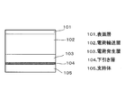
- FIG. 1 shows a layer structure of a general organic photoreceptor (OPC) as an image carrier. That is, the charge generation layer 103, the charge transport layer 102, and the surface layer 101 are laminated on the support 105 via the undercoat layer 104. The exposed light is absorbed by the charge generation layer 103 and generates charge carriers. The generated charge carriers are injected into the charge transport layer 2, to move the charge transport layer 102, to neutralize the dark potential V D. As a result, the exposed portion is attenuated to the bright potential VL , and an electrostatic latent image is formed.
- OPC organic photoreceptor
- the film thickness needs to be 20 ⁇ m or less (hereinafter referred to as thin film OPC).
- FIG. 2 shows the layer structure of the ⁇ -Si photosensitive member.
- a charge generation layer 113 a charge blocking layer 112, and a surface layer 111 are laminated on a support 115 via a charge blocking layer 114.
- the charge generation layer 113 can be formed in the vicinity of the surface layer 111, the diffusion of charges can be significantly suppressed.
- the film thickness needs to be 60 ⁇ m or less in order to realize an acceptable dot reproducibility in the ⁇ -Si photoreceptor.
- the ⁇ -Si photosensitive member has an extremely high hardness compared to OPC, and thus is sufficiently acceptable for the durability required in the printing market.
- examples of efforts to improve image quality include thinning a charge transport layer in an image carrier and an ⁇ -Si photoconductor.
- the ⁇ -Si photoreceptor can be said to be an image carrier that can output a high-quality image at a printing level and has durability required in the printing market.
- An example of an image forming apparatus using an ⁇ -Si photoconductor is described in Patent Document 1.
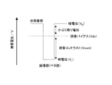
- FIG. 3 shows the latent image potential in the highest density portion (hereinafter, solid portion) in the image portion.
- a developing bias necessary for outputting the maximum density is applied to the solid portion of the bright potential VL .
- the DC component of the applied developing bias is referred to as Vdc
- Vcont developing contrast
- the solid portion is developed such that a potential generated by developing the toner (hereinafter, a charging potential ( ⁇ V)) fills the development contrast (Vcont).
- ⁇ V charging potential
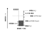
- Vcont The development ends normally when the charging potential has fully filled Vcont (FIG. 4).
- V D is the dark potential of the non-image portion
- the fog potential is between the dark potential (V D ) and the developing bias (Vdc).
- charge failure when the ⁇ -Si photoreceptor is used, the charge potential does not completely fill Vcont even at the end of development as shown in FIG. Such a phenomenon is called “charge failure”.
- Equation 1 The charging potential generated by developing the latent image with toner is theoretically expressed as Equation 1 as ⁇ Vth.
- dt toner layer height
- dm film thickness of image carrier (total film thickness excluding support)
- Q / S amount of toner charge per unit area
- ⁇ 0 dielectric constant of vacuum
- ⁇ t dielectric constant of toner layer
- ⁇ m relative permittivity of image carrier
- Equation 1 the first term is the potential ⁇ Vt created by the toner layer itself, and the second term is the potential ⁇ Vc created by the effect of the capacitor between the toner layer and the base layer of the image carrier.
- the sum of both terms becomes a potential generated when developing with toner, that is, a charging potential ⁇ Vth.
- ⁇ V is a measured value of the charging potential
- ⁇ Vth is a theoretical value of the charging potential (a value derived from Equation 1).
- the film thickness dm of the image carrier indicates the actual film thickness of the photosensitive layer, and indicates the film thickness of the layer excluding the support. Specifically, in the case of an ⁇ -Si photosensitive member, the film thickness dm of the image carrier includes the surface layer 111, the charge blocking layers 112 and 114, and the charge generation layer 113 excluding the support member 115 in FIG. Film thickness.
- the film thickness dm of the image carrier is a film thickness obtained by adding the surface layer 101, the charge transport layer 102, and the charge generation layer 103, excluding the support 105 and the undercoat layer 104 in FIG.
- the film thickness is obtained by adding the charge transport layer 102 and the charge generation layer 103.
- the undercoat layer 104 is formed on the support 105, the thickness dm of the image carrier does not include the thickness of the undercoat layer 104.
- the thin film OPC has a smaller thickness than the conventional film thickness, so that the capacitance increases, ⁇ Vc decreases, and as a result, charging failure tends to occur.
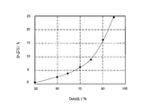
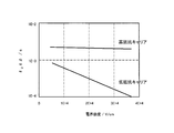
- FIG. 6 shows the amount of toner (mg / cm 2 ) on the image carrier in the solid portion at Vcont when the closest distance (hereinafter referred to as SD gap) between the developer carrier and the image carrier is 300 ⁇ m and 400 ⁇ m.
- SD gap the closest distance between the developer carrier and the image carrier.
- the OPC having a conventional film thickness (30 ⁇ m) has a charging efficiency of 100%, whereas the ⁇ -Si photosensitive member (30 ⁇ m) is reduced to 70%.
- SD 400 ⁇ m the amount of toner to be developed in OPC hardly changes, whereas the amount of toner to be developed in ⁇ -Si photoconductor has a large change.
- the charging rates were 100% (30 ⁇ m), 90% (25 ⁇ m), and 75% (20 ⁇ m), respectively.
- the film thickness of 30 ⁇ m (charging rate of 100%) and the film thickness of 25 ⁇ m (charging rate of 90%) with respect to the fluctuation of the SD gap of 100 ⁇ m showed little variation in the development amount, and the tolerance of stability. It turned out to be a level.
- the charging efficiency needs to be 90% or more.
- an object of the present invention is to provide an image forming apparatus capable of solving a charging failure without deteriorating fog and achieving both high image quality and high stability when using an image carrier having a high capacitance. It is.
- An image forming apparatus for achieving the above object includes an image carrier that carries an electrostatic image, A charging device for charging the image carrier; An exposure device that forms the electrostatic image by exposing the surface of the image carrier charged to a dark potential V D by the charging device and changing the surface to a light potential V L ; A developing device comprising a developer carrier for carrying a developer containing toner and a magnetic carrier; A power source for applying a developing bias to the developer carrying member, The developing bias, wherein the developer first peak voltages V 1 from the carrier generating an electrostatic force in the first direction toward the image bearing member to the toner, the image bearing member to said toner Is a vibration voltage that alternately repeats a second peak voltage V 2 that generates an electrostatic force in a second direction from the developer toward the developer carrying member, and a phase time for generating the electrostatic force in the first direction is T 1.
- the duty ratio Du (%) represented by (T2 / (T1 + T2)) ⁇ 100 is 60 ⁇ Du ⁇ 80
- the magnetic carrier is As the electric field strength increases, the resistivity ⁇ decreases and the relative dielectric constant ⁇ increases, Charge attenuation represented by a dielectric constant ⁇ 0 of vacuum, a relative dielectric constant ⁇ of the magnetic carrier, and a resistivity ⁇ at an electric field intensity E 2D determined by the second peak voltage V 2 and the dark potential V D
- the product of the time constant ⁇ 0 ⁇ ⁇ (s) and the electric field strength E 2D is 20 ⁇ ⁇ 0 ⁇ ⁇ E 2D (s ⁇ V / cm) is satisfied,
- the time constant ⁇ 0 ⁇ ⁇ (s) and the relative dielectric constant ⁇ at the electric field intensity E 1L determined by the first peak voltage V 1 and the bright potential VL are: ⁇ 0 ⁇ ⁇ (s) ⁇ 6.0 ⁇ 10
- FIG. 3 is a layer configuration model diagram of an example of an ⁇ -Si photosensitive member. It is a figure which shows a latent image electric potential. It is a figure which shows the latent image electric potential of a charge state. It is a figure which shows the latent image electric potential of a charging failure state. It is a figure which shows the relationship between the toner amount and Vcont in SD gap fluctuation. It is a wave form diagram which shows the bias used in the present Example. It is a figure which shows the relationship between the duty ratio of a duty wave, and a charging rate. It is a figure which shows the duty ratio and duty relationship of a duty wave.
- FIG. 1 is a schematic configuration diagram illustrating an embodiment of an image forming apparatus of the present invention. It is a figure which shows the latent image electric potential obtained with a surface potentiometer before development and after development. It is a figure which shows the charge potential after image development. It is a schematic diagram of an apparatus used for measurement of resistivity ⁇ ( ⁇ ⁇ cm) and relative permittivity ⁇ of a magnetic carrier. It is a figure which shows the Cole-Cole plot obtained by the measurement.
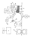
- FIG. 16 is a schematic configuration diagram of an example of an image forming apparatus.
- This image forming apparatus is a laser beam printer using an electrophotographic process, a digital image exposure system, and a reversal development system.
- Reference numeral 1 denotes a drum-type electrophotographic photosensitive member as an image carrier.
- the image carrier 1 has a high electrostatic capacity, and in particular, the electrostatic capacity per unit area (C / S) is C / S ⁇ 1.5 ⁇ 10 ⁇ 6 (F / m 2). )belongs to.
- the ⁇ -Si photosensitive member needs to be 60 ⁇ m or less, and the thin film OPC needs to be 20 ⁇ m or less.
- the value of the capacitance (C / S) is increased, as described above, charging failure is likely to occur. And, due to poor charging, the stability of development is extremely lowered.
- the image carrier 1 is an amorphous silicon photoconductor ( ⁇ -Si photoconductor).
- the ⁇ -Si photoreceptor basically comprises a photosensitive layer containing amorphous silicon on a conductive substrate.
- the photosensitive layer is formed of an amorphous silicon-based material such as Si, SiC, SiO, or SiON, and is formed by, for example, a glow discharge decomposition method, a sputtering method, an ECR method, or an evaporation method.
- Image bearing member 1 is rotated at a predetermined speed in the clockwise direction of arrow r, the surface is uniformly charged by a primary charger (charging device) 2 to a predetermined dark potential V D.
- Reference numeral 2 a denotes a charging bias application power source for the primary charger 2.
- Reference numeral 3 denotes a laser scanner (laser exposure apparatus) as digital exposure means. A time series electric digital pixel signal is input to the scanner 3 from a host device 11 such as an image scanner.
- an image signal obtained by a CCD or the like is digitized by an A / D converter and then sent to a signal processing unit to be converted into a binary image signal corresponding to the image density.
- the scanner 3 includes a laser driver, a laser, a polygon mirror, a mirror, and the like, and the image signal is input to the laser driver.
- the laser driver modulates the light emission of the laser in accordance with the input image signal.
- the dark potential surface of the image carrier 1 is subjected to scanning exposure L (image exposure) by the modulated laser light.
- the dark potential V D of the exposed portion attenuates to become a bright potential VL , and an electrostatic latent image is formed.
- the image exposure method is a method in which a portion of an image carrier to which toner is to be adhered is exposed in advance during development, and a light potential portion of the image carrier is developed with toner.
- Reference numeral 4 denotes a developing device that develops an electrostatic latent image formed on the surface of the image carrier 1 as a toner image.
- the developing device 4 of this example is a reversal developing device using a two-component developer A composed of a magnetic carrier and a nonmagnetic toner as a developer. The weight ratio between the toner and the carrier is adjusted to a predetermined value.
- the developer A is accommodated in the developing container 4a, and is agitated by the agitating member 4b, so that the toner is triboelectrically charged to a negative polarity.
- the developer A is supplied to a developing sleeve 4c as a developer carrying member.
- the developing sleeve 4c is driven to rotate at a predetermined speed in the counterclockwise direction of the arrow.
- a magnet roller 4d made of a magnetic material having a plurality of magnetic poles is disposed in the developing sleeve 4c.
- the developer A supplied to the developing sleeve 4c is carried on the surface of the developing sleeve 4c as a magnetic brush layer by the magnetic force of the magnet roller 4d, and is conveyed by the rotation of the developing sleeve 4c.
- the blade 4e is subjected to the regulation of the layer thickness, and the film is conveyed to a development area which is a facing portion between the developing sleeve 4c and the image carrier 1.
- a predetermined developing bias is applied to the developing sleeve 4c from a developing bias applying power source 4f.
- a developing electric field is generated in the developing area, the toner adhering to the carrier is pulled away from the carrier, and the electrostatic latent image on the image carrier 1 side is reversely developed with negative toner.
- the polarity at which the image carrier is charged by the charger and the charging polarity of the toner are the same.
- the developer magnetic brush layer subjected to development in the development area is conveyed back into the developing container 4a by the subsequent rotation of the developing sleeve 4c, and is magnetically peeled off from the surface of the developing sleeve 4c. Then, a fresh developer is supplied to the developing sleeve 4c.
- the developer A in the developer container 4a is reduced in toner density as the toner is consumed by development.
- the toner concentration in the developer A in the developing container 4a is monitored by a sensor (not shown). When the toner concentration falls to the allowable lower limit concentration, an operation of supplying an appropriate amount of toner from the replenishing toner container 4g to the developer A in the developing container 4a is intermittently executed. Thereby, the toner density is maintained within a predetermined range.
- the toner image formed on the image carrier 1 is fed by a transfer charger 5 as a transfer device from a paper supply unit (not shown) to a facing portion between the image carrier 1 and the transfer charger 5 at a predetermined control timing.
- a transfer charger 5 as a transfer device from a paper supply unit (not shown) to a facing portion between the image carrier 1 and the transfer charger 5 at a predetermined control timing.
- a recording material (transfer material) P such as a sheet.
- a positive transfer bias that is opposite to the toner charging polarity is applied to the transfer charger 5 at a predetermined control timing from a transfer bias application power source 5a.
- the toner image on the image carrier 1 side is electrostatically transferred onto the surface of the recording material P.
- the recording material P that has passed through the transfer portion is separated from the surface of the image carrier 1 and introduced into the fixing device 8.
- the fixing device 8 fixes the unfixed toner image on the recording material P as a permanently fixed image with heat and pressure, and discharges the recording material P.
- the image carrier 1 after separation of the recording material is wiped off by a cleaning blade 6a of a cleaner 6 and subjected to a removal process of residual adhering matters such as transfer residual toner, and further subjected to full exposure by a pre-exposure device 7 to remove static electricity. And repeatedly used for image formation.
- control circuit unit 9 is a control circuit section (control means).
- the control circuit unit 9 performs processing of signals input from various process devices of the image forming apparatus, command signals to the various process devices, and predetermined image forming sequence processing.
- the apparatus is controlled according to a control program and a reference table stored in the ROM.
- Various image forming conditions are input from the operation panel unit 10 to the control circuit unit 9.
- Various information is input from the control circuit unit 9 to the operation panel unit 10 and displayed on the display unit.
- the charging efficiency is a ratio of the charging potential ⁇ V with respect to the development contrast Vcont, as expressed in Expression 3.
- Vcont is a potential difference between the DC component of the developing bias and the bright potential VL of the portion to be the image portion of the image carrier.
- ⁇ V is a potential difference between the toner layer surface potential after development of the latent image potential portion and the latent image potential before development. That is, the ⁇ V of the image carrier corresponding to the solid image portion is the surface potential of the toner layer after development of the light potential portion, which is the portion of the image carrier corresponding to the solid image portion, and the image carrier corresponding to the solid image portion.
- This is the potential difference from the bright potential before development, which is the portion of The potentials such as the bright potential and the toner layer potential were measured with a surface potential meter at or near the development position.
- the surface potential meter used here is MODEL347 manufactured by Trek.
- a method for measuring the charging efficiency will be described. First, an empty developing device 4 that does not contain the two-component developer A is prepared, and the surface potential (latent image potential before development) on the image carrier 1 that has not been developed with toner after charging and latent image formation is developed. Measurements are made with a surface potentiometer 12 arranged directly under the apparatus.
- a developing device 4 containing the two-component developer A is prepared, and a toner image is actually formed on the image carrier 1 by applying a developing bias after charging and latent image formation.
- the surface potential meter 12 measures the potential on the surface of the image carrier immediately after development (latent image potential after development).
- FIG. 17 shows potential profiles of the latent image potential before development and the latent image potential after development obtained by the above two methods.
- FIG. 18 by subtracting the surface potential values of the pre-development latent image potential and the post-development latent image potential, it is possible to obtain ⁇ V produced by actually developing the toner.
- the ratio of ⁇ V to Vcont at this time is the charging efficiency (Formula 3).
- Vcont is determined at the development position. That is, a dedicated surface potential meter is installed at the position of the developing device 4, the latent image potential at the developing position is measured, Vdc is determined for the latent image potential, and Vcont at the developing position is guaranteed.
- FIG. 19 is a schematic diagram of an apparatus used for measurement.
- This device uses a modified Canon IRC-6800 multifunction device.
- the photosensitive drum of this multi-function machine is replaced with a ⁇ 84 mm aluminum cylindrical body 201 (hereinafter referred to as an Al drum) having no photosensitive layer so that it can be rotated.
- the A1 drum rotates at a peripheral speed of 286 mm / sec.
- the developer 203 of the modified machine is filled with the magnetic carrier 202 to be measured alone.
- a ⁇ 20 mm developing sleeve 231 carrying the magnetic carrier 202 is opposed to the Al drum.
- the developing sleeve 231 rotates so as to move in the same direction as the A1 drum at the portion facing the A1 drum, and its peripheral speed is 500 mm / sec.
- the A1 drum and the developing sleeve are positioned so as to form a 300 ⁇ m gap (SD gap) at the opposing portion.
- An equivalent circuit is derived from a Cole-Cole plot (see FIG. 20) plotting each measured value (Re (Z), Ima (Z)) when the frequency is changed from 1 Hz to 10 kHz.
- the Cole-Cole plot is a semicircle as shown in FIG. 20, it indicates that the equivalent circuit of the magnetic carrier is a parallel circuit of RC.
- the R component and the C component of the magnetic carrier can be obtained by fitting with an RC parallel circuit by the analysis software (Zview) manufactured by Solartron.
- the capacitance Ct obtained by the above analysis method includes the influence of the air layer (relative dielectric constant 1) outside the development region (hereinafter, development nip) in the development sleeve 231 and the Al drum 201. That is, in order to obtain the capacitance C of the magnetic carrier 202, it is necessary to subtract the capacitance Ca due to the air layer outside the development nip from the capacitance Ct obtained by the above analysis method.
- a method for deriving Ca will be described.
- An empty developing device 203 that does not contain the magnetic carrier 202 is measured by the above measuring method.
- Cat obtained by the above analysis method is a composite value of the electrostatic capacity Can due to the air layer in the developing nip and the electrostatic capacity Ca due to the air layer outside the developing nip.
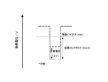
- the resistivity of the magnetic carrier 202 is determined from the SD gap (cm) and the contact area (cm 2 ) of the magnetic carrier 202 with respect to the Al drum 201.
- ⁇ ( ⁇ ⁇ cm) and relative dielectric constant ⁇ were determined.
- required by the said measuring method is used for the dielectric constant (epsilon) and resistivity (rho) of the magnetic carrier in the claim of this application. That is, the relative permittivity ⁇ and resistivity ⁇ of the magnetic carrier used in this claim are not the physical property values of the magnetic carrier alone, but the relative permittivity ⁇ including the magnetic carrier and the air layer present in the development nip, It represents the resistivity ⁇ .
- the resistivity ⁇ and the relative dielectric constant ⁇ determined by the above measurement method do not take toner into consideration.
- Each physical property value of the two-component developer actually mixed with the toner is expected to be different.
- the influence of the toner is considered to be small in each physical property value in the development nip. Therefore, in the present invention, the toner is not taken into account in defining the resistivity ⁇ and the dielectric constant ⁇ .
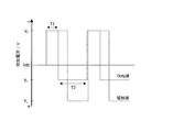
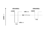
- the electric field strength under development bias application is determined as follows. For example, in the case of the developing bias as shown in FIG. 7, the phase time for moving the toner in the direction of the image carrier is T1, and the phase time for moving the toner in the direction of the developer carrier is T2.
- the resistivity ⁇ and relative dielectric constant ⁇ of the magnetic carrier under the application of a developing bias were obtained by the measurement method (5) based on the resistivity ⁇ and relative dielectric constant ⁇ at the electric field strength.
- Example 1 Chargeability and fogging were measured under a fixed image output condition for magnetic carriers having different physical property values ( ⁇ , ⁇ ). The verification result will be described. Development was carried out using a digital-image exposure method and a reversal development method using a modified machine of the above-mentioned IRC-6800 (a model of a copy complex machine manufactured by Canon Inc.).
- the film thickness dm, the capacitance C / S per unit area, and the relative dielectric constant ⁇ m were measured by the measurement method (2).
- the image carrier is uniformly charged at the development position by the primary charger 2 shown in FIG. 16 at the development position, and the surface of the image carrier 1 is uniformly charged to a desired dark potential V D ( ⁇ 480 V).
- the solid portion potential was adjusted to a desired light potential V L ( ⁇ 130 V).
- the distance (SD gap) between the developing sleeve 4c and the image carrier 1 is 300 ⁇ m.
- the developing bias used at this time has a waveform in which an AC component is superimposed on a DC component as shown in FIG.
- the duty wave has a frequency of 5 kHz, a duty ratio of 60%, and a peak-to-peak voltage (hereinafter referred to as Vpp) of 1.54 kV.
- the DC component Vdc is a required development contrast (200 V) with respect to the electrostatic latent image of the image carrier, specifically, the bright potential V L ( ⁇ 130 V) and the dark potential V D ( ⁇ 480 V) corresponding to the solid portion.
- the development contrast is a difference between Vdc and the bright potential V L
- the fog removing potential is a difference between Vdc and the dark potential V D.
- the frequency is 5 kHz, but the frequency is preferably 3 kHz to 8 kHz. According to the study by the inventors, when the frequency is less than 3 kHz, the fogging does not reach the allowable level under any condition, and when the frequency is higher than 8 kHz, the chargeability does not reach the allowable level under any condition. all right.
- the developer used in the present invention a two-component developer having a nonmagnetic toner and a magnetic carrier is used.
- a toner prepared by a conventionally known pulverization method was used.
- the magnetic carrier used three types of carriers having different physical property values ( ⁇ , ⁇ ) were prepared. Specific features are listed below.
- High dielectric constant (low resistance) carrier A examples include those using magnetite and ferrite having magnetism represented by the following formula (1) or (2) as a core material.
- M examples include Be, Mg, Ca, Rb, Sr, V, Cr, Mn, Fe, Co, Ni, Cu, Zn, Y, Zr, Nb, Mo, Cd, Pb, and Li. Or it can be used in plural.
- metal compound particles having magnetism include Cu—Zn—Fe ferrite, Mn—Mg—Fe ferrite, Mn—Mg—Sr—Fe ferrite, and Li—Fe ferrite.
- metal compound particles having magnetism include Cu—Zn—Fe ferrite, Mn—Mg—Fe ferrite, Mn—Mg—Sr—Fe ferrite, and Li—Fe ferrite.
- iron-based oxides examples include iron-based oxides.
- a known method can be employed as a method for producing the ferrite particles.
- a ferrite, pulverized to a submicron size is mixed with a binder, water, a dispersant, and the like, and particles are formed using a spray dryer method or a fluidized granulation method.
- firing is performed at a temperature in the range of 700 to 1400 ° C., preferably 800 to 1300 ° C. in a rotary kiln or batch-type firing furnace.
- the particles are classified by sieve to control the particle size distribution to obtain core particles for carriers.
- a resin such as a silicone resin is coated on the surface of the ferrite particles by a dipping method.
- the magnetic carrier thus produced is referred to as a high dielectric constant carrier A here.
- Low dielectric constant (high resistance) carrier B examples include the following. First, a magnetic material-dispersed resin carrier produced by melt-kneading and pulverizing magnetite particles and a thermoplastic resin is used as a core material.
- a magnetic material-dispersed resin carrier produced by spray-drying a slurry obtained by melting and dispersing magnetite particles and a thermoplastic resin in a solvent using a spray dryer or the like is used as a core material.
- a magnetic material-dispersed resin carrier obtained by reaction-curing phenol by direct polymerization in the presence of magnetite particles and hematite particles is used as a core material.
- carrier core materials are further coated with about 1.0 to 4.0% by mass of a resin such as a thermoplastic resin using a fluidized bed coating apparatus or the like.
- the magnetic carrier thus produced is referred to as a low dielectric constant carrier B here.
- Carrier C according to the present invention for example, a porous resin-filled carrier in which a resin such as a silicone resin is poured into a porous core and the voids in the core are filled with the resin can be used.
- a resin such as a silicone resin
- Examples of a method for producing the carrier C include the following methods. First, a metal oxide selected from the group consisting of Ni, Cu, Zn, Li, Mg, Mn, Sr, Ca, and Ba as used in the high dielectric constant carrier A, iron oxide ( A predetermined amount of Fe 2 O 3 ) is weighed and mixed.
- the obtained mixture is calcined in the range of 700 to 1000 ° C. for 5 hours, and then pulverized to a particle size of about 0.3 to 3 ⁇ m.
- a binder, water, a dispersant, and if necessary, pore forming agents such as organic fine particles and Na 2 CO 3 are added and spray-dried with a spray dryer in a heated atmosphere of 100 to 200 ° C., Granulate to a size of about 20-50 ⁇ m.
- the silicone resin is filled in an amount of 8 to 15% by mass under reduced pressure, and the silicone resin is cured in an inert gas atmosphere at 180 to 220 ° C. If necessary, a resin such as a thermosetting resin is further coated (coated) by about 0.1 to 5.0% by mass by an immersion method.
- an inert gas for example, N 2 gas
- the dielectric constant of the carrier is controlled by controlling the porosity of the core, the resistance of the core material, the amount of resin such as silicone resin to be filled, and the amount of coating resin as the coating resin.
- ⁇ and resistivity ⁇ can be controlled.
- the phase time at which the electrostatic force in the first direction from the developer carrier toward the image carrier is generated with respect to the toner for one period is the peak at T1 and T1.
- the phase generating electrostatic force in a second direction toward the developer carrying member, direction, and time to peak voltage at T2, T2 and a second peak voltage V 2 from the image bearing member to the toner, V 1 and V Repeat 2 alternately.
- the duty (Duty) ratio the proportion of T2 occupied in one period (hereinafter referred to as the duty (Duty) ratio).
- the value of V1 and V2 and T1 are set so that the integrated value of the waveform when Vdc in the period T1 is the reference axis and the integrated value of the waveform with the Vdc as the reference axis in the period T2 are the same value.
- the oscillating bias weaken the pull-back direction of the peak voltage V 2 (hereinafter referred to as the duty (Duty) waves).
- the duty ratio (Du) (%) is calculated by the relational expression of (T2 / (T1 + T2)) ⁇ 100.
- Such a duty wave causes the toner to be localized in the vicinity of the image carrier in order to weaken the force to pull the toner back toward the developer carrier at the phase time T2. As a result, the amount of toner finally developed on the image carrier increases, and charging failure is improved.
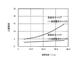
- FIG. 8 is a diagram showing a change in chargeability when the duty ratio Du of the duty wave is varied using the carrier A.
- FIG. 8 For the above reasons, as the duty ratio Du is increased, the chargeability is dramatically improved as compared with the rectangular wave (duty ratio 50%). However, when the duty ratio exceeds 80%, the phase time for moving the toner in the direction of the developer carrier becomes too long compared with the time for moving the toner in the direction of the image carrier, and as a result, the toner moves in the direction of the image carrier. The chargeability is greatly reduced. In addition, even if this characteristic was examined by changing the type of carrier as shown in FIG. 12, the result of the same tendency was obtained.
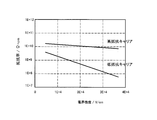
- FIG. 9 is a diagram showing the change in fog when the duty ratio Du of the duty wave is varied for the image forming apparatus using the carrier A and including the ⁇ -Si photosensitive member.
- the reflection density Ds of the image white background portion (non-image portion) is measured by a reflection densitometer (SERISE 1200) manufactured by Macbeth.
- FIG. 10 shows the relationship between the fog and the duty ratio Du when the resistance of the magnetic carrier to be used is varied with respect to the ⁇ -Si photosensitive member.
- the low resistance carrier is the carrier A described above
- the high resistance carrier is the carrier B described above.
- the magnetic carrier can be regarded as an RC parallel circuit including a resistance component R and a capacitance component C.
- a charge Qc (hereinafter referred to as counter charge) having a polarity opposite to that of the toner charge is stored in the capacitive component of the magnetic carrier.
- the counter charge attenuates with a time constant of ⁇ as shown in Equation 2.
- the fog is a time constant of charge decay represented by the relative permittivity ⁇ and resistivity ⁇ of the magnetic carrier at the electric field strength E 2D in the phase in which the toner is moved to the developer carrying member. It was confirmed that there is a correlation between the product of ⁇ 0 ⁇ ⁇ (s) and the electric field strength E 2D .
- FIG. 11 shows the relationship of fogging to ⁇ 0 ⁇ ⁇ E 2D (s ⁇ V / cm). As shown in FIG. 11, the fog is improved as ⁇ 0 ⁇ E 2D increases, and 20 When ⁇ ⁇ 0 ⁇ E 2D (s ⁇ V / cm), it was confirmed that the fogging reached an allowable level (2% or less).
- the upper limit is set to the value of ⁇ 0 ⁇ E 2D There is no.
- Fog level and this time t, is considered to be due to the electric field strength E 2D moving the developer carrying member direction. For the above reasons, it is considered that the fog and ⁇ 0 ⁇ ⁇ E 2D are correlated.
- the reason why the fog is improved by increasing the resistance ( ⁇ ) of the magnetic carrier is considered to be that ⁇ 0 ⁇ of the magnetic carrier is increased and the time for holding the necessary counter charge is increased. This remaining counter charge collects weakly charged fog toner adhering to the non-image area, which is considered to improve the fog.
- FIG. 12 shows the relationship between chargeability and duty ratio when the resistance of the magnetic carrier is varied. As shown in FIG. 12, the chargeability deteriorates by increasing the resistance of the magnetic carrier.
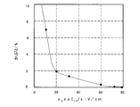
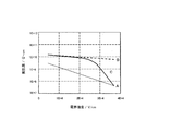
- FIG. 13 shows the electric field strength dependence of the resistivity of the high-resistance carrier and the low-resistance carrier used above. As the electric field strength increases, the resistivity decreases.
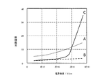
- FIG. 14 shows the electric field strength dependence of the relative permittivity of these magnetic carriers.
- the relative permittivity of the magnetic carrier decreases accordingly.
- FIG. 15 shows the relationship between ⁇ 0 ⁇ ⁇ (s) obtained from the resistivity ⁇ and the relative dielectric constant ⁇ , and the electric field strength. The reason why the chargeability deteriorates when the resistance of the magnetic carrier is increased can be explained as follows from the above physical property values.
- the relative permittivity itself affects the chargeability. Specifically, the chargeability of a magnetic carrier having a small relative dielectric constant is lower than that of a magnetic carrier having a large relative dielectric constant. This can be explained by regarding the developing sleeve and the image carrier as parallel plates.
- the dielectric constant of the magnetic carrier when there is a magnetic carrier between the developing sleeve and the image carrier, the larger the dielectric constant of the magnetic carrier, the larger the electric field applied to the periphery of the magnetic carrier, and the easier the toner will fly from the magnetic carrier.
- the dielectric constant when the dielectric constant is small, it is difficult for the toner to fly from the magnetic carrier, and as a result, the chargeability is considered to deteriorate.
- the measurement results of the electric field strength dependence of the resistivity ⁇ and the relative dielectric constant ⁇ of the high dielectric constant carrier A, the low dielectric constant carrier B, and the carrier C according to the present invention are shown in FIGS.
- the high dielectric constant carrier A the resistivity ⁇ decreased and the relative dielectric constant ⁇ increased as the electric field strength increased.
- the low dielectric constant carrier B has a very small change in both resistivity ⁇ and relative dielectric constant ⁇ as the electric field strength increases.
- the carrier C according to the present invention has a small rate of change with increasing electric field strength in the vicinity of a predetermined electric field strength, in this example, up to about 2.6 ⁇ 10 4 (V / cm).
- carrier C has a resistivity decrease rate with respect to a change in electric field strength at a field strength greater than a predetermined electric field strength, and a decrease rate of resistivity with respect to a change in electric field strength at an electric field strength smaller than the predetermined electric field strength. Has great properties.
- carrier C has an increase rate of relative dielectric constant with respect to a change in electric field strength at a field strength smaller than the predetermined electric field strength, and an increase rate of relative dielectric constant with respect to a change in electric field strength at a smaller electric field strength than the predetermined electric field strength.
- Increase rate of relative dielectric constant with respect to a change in electric field strength at a field strength smaller than the predetermined electric field strength and an increase rate of relative dielectric constant with respect to a change in electric field strength at a smaller electric field strength than the predetermined electric field strength.
- the change in the physical property values is considered to be caused by the following.
- the core material is formed of a conductive material like the high dielectric constant carrier A
- the electrical property values ( ⁇ , ⁇ ) change as the electric field strength increases.
- the core since the core has a porous structure formed of a conductive material and is filled with an insulating resin, the core has an insulating resin portion. There is a conductive porous part.
- the flow of charges can be blocked to some extent at the boundary between the insulating resin portion and the conductive porous portion.
- the limit value that can be cut off in this case, the electric field strength of 2.6 ⁇ 10 4 (V / cm)
- V / cm the electric field strength of 2.6 ⁇ 10 4
- ⁇ the relative dielectric constant ⁇ and resistivity of the magnetic carrier
- the relative dielectric constant ⁇ and resistivity of the magnetic carrier can be controlled by controlling the porosity of the core, the resistance of the core material, and the amount of resin such as silicone resin to be filled and the amount of resin of the coating resin. ⁇ can be controlled. It is also possible to control the limit value.
- the electric field strength E 2D in the pullback direction is 2.6 ⁇ 10 4 (V / cm), and until this vicinity, the resistivity ⁇ is large and the relative permittivity ⁇ is small.
- the electrolytic strength E 1L in the developing direction is 3.7 ⁇ 10 4 [V / cm], and in the region where the characteristic change is large, the resistivity ⁇ is greatly reduced to the same level as the low-resistance carrier A, and the relative dielectric constant
- the rate ⁇ increases rapidly and is a value that greatly exceeds the relative dielectric constant of the high dielectric constant carrier A.
- the two-component developer used in the present invention was adjusted so that the triboelectric charge amount of toner was equal. Specifically, the mixing ratio of the non-magnetic toner and the magnetic carrier was varied. Actually, the weight percentage of the non-magnetic toner relative to the total weight was 8% to 10%. At this time, the triboelectric charge amount (hereinafter referred to as Q / M) of the toner was about ⁇ 50 ⁇ C / g.
- a Faraday gauge 300 shown in FIG. 23 includes a double cylinder in which a metal inner cylinder 301 and an outer cylinder 302 having different shaft diameters are arranged coaxially, and a filter 303 for further taking toner into the inner cylinder 301. It has.
- the inner cylinder 301 and the outer cylinder 302 are insulated by an insulating member 302.
- the induced charge amount Q was measured, and the value divided by the toner weight M in the inner cylinder 301 was defined as Q / M ( ⁇ C / g).
- a measuring instrument “KEITHLEY 616 DIGITAL ELECTROMETER” manufactured by Keithley Instruments Inc. was used. Table 1 shows the results of evaluation of each charging rate and fog when using the high dielectric constant carrier A, the low dielectric constant carrier B, and the carrier C according to the present invention under the above conditions.
- the reflection density Ds of the image white background is measured with a reflection densitometer (SERISE 1200) manufactured by Macbeth.
- the reflection density Dr of the paper itself was measured in the same manner, and the fog density was determined as follows.
- Fog density (%) Dr-Ds
- the obtained fog density was evaluated according to the following evaluation criteria. A: 0.5% or less ... very good B: 0.6 to 1% or less ... good C: 1 to 2.0% or less ... acceptable level D: 2% to ... bad
- the carrier C according to the present invention was the only magnetic carrier that satisfies both the charging rate and the fog.
- Example 2 In Example 2, in order to clarify the relationship between the carrier physical properties ( ⁇ , ⁇ ), the charging rate, and the fogging, the magnetic carriers D to H were added to Example 1 for investigation. Carriers D to H were prepared by the same manufacturing method as carrier C. At this time, the relative dielectric constant ⁇ and resistivity ⁇ of the carrier are controlled by controlling the porosity of the core, the resistance of the core material, the amount of resin such as silicone resin to be filled, and the amount of resin of the coating resin. Control was performed as follows. The measurement results of physical property values ( ⁇ , ⁇ 0 ⁇ ⁇ ), fogging and charging rate of the magnetic carriers A to H are as follows. The dielectric constant ⁇ 0 of the vacuum is a constant.
- the carriers C, D, and E were the magnetic carriers in which the fogging was at an acceptable level and the charging rate was 90% or more.
- the reason is considered as follows.
- the magnetic carriers satisfying the allowable level of fog were carriers B, C, D, E, G, and H. These magnetic carriers have an electric field strength of E 2D (V / cm). 20 ⁇ ⁇ 0 ⁇ ⁇ E 2D (s ⁇ V / cm) Meet.
- the counter charge remaining in the magnetic carrier is sufficiently large at the electric field intensity E 2D determined by the phase time T2 for moving the developing bias toner in the direction of the developer carrying member with respect to the non-image portion (V D ).
- the fog toner adhered to the non-image portion can be collected.
- carriers C, D, E, and F satisfy the allowable level of charge rate. These carriers satisfy ⁇ 0 ⁇ (s) ⁇ 6.0 ⁇ 10 ⁇ 4 and 30 ⁇ ⁇ at electric field intensity E 1L (V / cm). For this reason, the counter charge remaining on the magnetic carrier is sufficiently small at the electric field intensity E 1L applied at the phase time T1 for moving the developing bias toner in the direction of the image carrier relative to the image portion (V L ).
- the time constant ⁇ 0 ⁇ (s) is easily lost, and the inhibition of the toner flight movement due to the counter charge can be prevented. Thereby, the chargeability in an image part can be improved.
- the relative permittivity ⁇ of the magnetic carrier is set to a large value of 30 or more, the electric field applied to the periphery of the magnetic carrier becomes large, and the toner can easily fly from the magnetic carrier.
- the value of the dielectric constant ⁇ the larger the electric field is, the more the flight is promoted. Therefore, there is no upper limit to the value of the dielectric constant ⁇ from the viewpoint of improving the charging failure.
- the carriers C, D and E according to the present invention satisfy the scope of claim 1 of the present application.
- Example 3 In order to vary E 2D while the electric field strength E 1L of Example 2 was fixed at 3.7 ⁇ 10 4 [V / cm], the duty ratio and Vpp were changed to 70% and 1.33 kV, respectively, and the same. Was examined.
- the duty wave has a frequency of 5 kHz, a duty ratio of 70%, and a Vpp of 1.33 kV.
- Table 3 shows the measured physical property values ( ⁇ , ⁇ 0 ⁇ ), fogging and charging rate of the magnetic carriers A to G at this time.
- the carriers C, D, and E are the magnetic carriers that have an acceptable level of fogging and a charge rate of 90% or more.
- the magnetic carriers satisfying the allowable level of fog were carriers B, C, D, E, G, and H. These magnetic carriers have an electric field strength E 2D (V / cm) of 20 ⁇ ⁇ 0 ⁇ ⁇ E 2D [s ⁇ V / cm] is satisfied. For this reason, the counter charge remaining in the magnetic carrier is sufficiently large at the electric field intensity E 2D determined by the phase time T2 for moving the developing bias toner in the direction of the developer carrying member with respect to the non-image portion (V D ). By this counter charge, the fog toner adhered to the non-image portion can be collected.
- carriers C, D, E, and F satisfy the allowable level of charge rate. These carriers satisfy ⁇ 0 ⁇ (s) ⁇ 6.0 ⁇ 10 ⁇ 4 and 30 ⁇ ⁇ at the electric field strength E 1L (V / cm). For this reason, the counter charge remaining on the magnetic carrier is sufficiently small at the electric field intensity E 1L applied at the phase time T1 for moving the developing bias toner in the direction of the image carrier relative to the image portion (V L ). Counter charge can inhibit the movement of the toner and reduce the chargeability.
- the relative permittivity ⁇ of the magnetic carrier is sufficiently large, the electric field applied to the periphery of the magnetic carrier is increased, and the toner can easily fly from the magnetic carrier. From the above, only the carriers C, D and E according to the present invention satisfy the scope of claim 1.
- Example 4 In order to vary E 2D while the electric field intensity E 1L of Example 2 was fixed at 3.7 ⁇ 10 4 [V / cm], the duty ratio and Vpp were changed to 80% and 1.16 kV, respectively.
- the duty wave has a frequency of 5 kHz, a duty ratio of 80%, and a Vpp of 1.16 kV.
- the physical property values ( ⁇ , ⁇ 0 ⁇ ⁇ ), fogging and charging rate of the magnetic carriers A to G are as follows.
- Carriers C, D, and E are magnetic carriers that have an acceptable level of fog and a charge rate of 90% or more.
- the magnetic carriers satisfying the allowable level of fog were carriers B, C, D, E, G, and H. These magnetic carriers have an electric field strength of E 2D (V / cm). 20 ⁇ ⁇ 0 ⁇ ⁇ E 2D (s ⁇ V / cm) Meet.
- the counter charge remaining in the magnetic carrier is sufficiently large at the electric field intensity E 2D determined by the phase time T2 for moving the developing bias toner in the direction of the developer carrying member with respect to the non-image portion (V D ). Therefore, the fog toner adhered to the non-image portion can be collected by this counter charge.
- carriers C, D, E, and F satisfy the allowable level of charge rate. These carriers have ⁇ 0 ⁇ (s) ⁇ 6.0 ⁇ 10 ⁇ 4 and 30 ⁇ ⁇ at electric field strength E 1L (V / cm). Meet.
- the counter charge remaining on the magnetic carrier is sufficiently small at the electric field intensity E 1L applied at the phase time T1 for moving the developing bias toner in the direction of the image carrier relative to the image portion (V L ). Therefore, it is possible to reduce the deterioration of the chargeability by inhibiting the movement of the toner by the counter charge.
- the relative permittivity ⁇ of the magnetic carrier is sufficiently large, the electric field applied to the periphery of the magnetic carrier is increased, and the toner can easily fly from the magnetic carrier.
- Example 5 To vary the electric field strength E 1L in Example 2, the duty ratio, Vpp, respectively, 60%, was subjected to the same examination instead 0.85KV. Specifically, the duty wave has a frequency of 5 kHz, a duty ratio of 60%, and a Vpp of 0.85 kV.
- the magnetic carrier with which the fogging is at an acceptable level and the charging rate is 90% or more was carrier I.
- the magnetic carriers satisfying the allowable level of fog were carriers I, K, and L. These magnetic carriers have an electric field strength of E 2D (V / cm). 20 ⁇ ⁇ 0 ⁇ ⁇ E 2D (s ⁇ V / cm) Meet.
- the counter charge remaining in the magnetic carrier is sufficiently large at the electric field intensity E 2D determined by the phase time T2 for moving the developing bias toner in the direction of the developer carrying member with respect to the non-image portion (V D ). Therefore, the fog toner adhered to the non-image portion can be collected by this counter charge.
- carriers satisfying the allowable level of the charging rate were carriers I and J. These carriers have electric field strength E 1L (V / cm), ⁇ 0 ⁇ (s) ⁇ 6.0 ⁇ 10 ⁇ 4 and 30 ⁇ ⁇ are satisfied.
- the counter charge remaining on the magnetic carrier is sufficiently small at the electric field intensity E 1L applied at the phase time T1 for moving the developing bias toner in the direction of the image carrier relative to the image portion (V L ). Therefore, it is possible to reduce the deterioration of the chargeability by inhibiting the movement of the toner by the counter charge.
- the relative permittivity ⁇ of the magnetic carrier is sufficiently large, the electric field applied to the periphery of the magnetic carrier is increased, and the toner can easily fly from the magnetic carrier. From the above, only the carrier I according to the present invention satisfies the scope of claim 1.
- Example 6 In order to vary E 2D while the electric field strength E 1L of Example 5 was fixed at 2.3 ⁇ 10 4 (V / cm), the duty ratio and Vpp were changed to 70% and 0.74 kV, respectively. Was examined.
- the duty wave has a frequency of 5 kHz, a duty ratio of 70%, and Vpp 0.74 kV.
- the magnetic carrier with which the fogging is at an allowable level and the charging rate is 90% or more is Carrier I.
- the magnetic carriers satisfying the allowable level of fog were carriers I, K, and L. These magnetic carriers have an electric field strength of E 2D (V / cm). 20 ⁇ ⁇ 0 ⁇ ⁇ E 2D (s ⁇ V / cm) Meet. For this reason, the counter charge remaining in the magnetic carrier is sufficiently large at the electric field intensity E 2D determined by the phase time T2 for moving the developing bias toner in the direction of the developer carrying member with respect to the non-image portion (V D ). Therefore, the fog toner adhered to the non-image portion can be collected by this counter charge.
- carriers satisfying the allowable level of the charging rate were carriers I and J. These carriers have electric field strength E 1L (V / cm), ⁇ 0 ⁇ (s) ⁇ 6.0 ⁇ 10 ⁇ 4 and 30 ⁇ ⁇ Meet.
- the counter charge remaining on the magnetic carrier is sufficiently small at the electric field intensity E 1L applied at the phase time T1 for moving the developing bias toner in the direction of the image carrier relative to the image portion (V L ). Therefore, it is possible to reduce the deterioration of the chargeability by inhibiting the movement of the toner by the counter charge.
- the relative permittivity ⁇ of the magnetic carrier is sufficiently large, the electric field applied to the periphery of the magnetic carrier is increased, and the toner can easily fly from the magnetic carrier. From the above, only the carrier I according to the present invention satisfies the scope of claim 1.
- Example 7 In order to vary E 2D while the electric field intensity E 1L of Example 5 was fixed at 2.3 ⁇ 10 4 (V / cm), the duty ratio and Vpp were changed to 80% and 0.67 kV, respectively. Was examined. Specifically, the duty wave has a frequency of 5 kHz, a duty ratio of 80%, and a Vpp of 0.67 kV.
- E 2D 1.0 ⁇ 10 4 (V / cm) Met.
- the magnetic carrier that has an acceptable level of fogging and a charge rate of 90% or more was carrier I.
- the magnetic carriers satisfying the allowable level of fog were carriers I, K, and L. These magnetic carriers have an electric field strength E 2D (V / cm) of 20 ⁇ ⁇ 0 ⁇ ⁇ E 2D (s ⁇ V / cm) is satisfied.
- the counter charge remaining in the magnetic carrier is sufficiently large at the electric field intensity E 2D determined by the phase time T2 for moving the developing bias toner in the direction of the developer carrying member with respect to the non-image portion (V D ). Therefore, the fog toner adhered to the non-image portion can be collected by this counter charge.
- carriers satisfying the allowable level of the charging rate were carriers I and J. These carriers have electric field strength E 1L (V / cm), ⁇ 0 ⁇ ⁇ (s) ⁇ 6.0 ⁇ 10 ⁇ 4 and 30 ⁇ ⁇ Meet.
- the counter charge remaining on the magnetic carrier is sufficiently small at the electric field intensity E 1L applied at the phase time T1 for moving the developing bias toner in the direction of the image carrier relative to the image portion (V L ). Therefore, it is possible to reduce the deterioration of the chargeability by inhibiting the movement of the toner by the counter charge.
- the relative permittivity ⁇ of the magnetic carrier is sufficiently large, the electric field applied to the periphery of the magnetic carrier is increased, and the toner can easily fly from the magnetic carrier. From the above, only the carrier I according to the present invention satisfies the scope of claim 1.
- the carrier ⁇ 0 ⁇ ⁇ (s) is controlled so as to satisfy the following equation. That is, the relative permittivity ⁇ and resistivity ⁇ of the magnetic carrier are controlled so as to satisfy ⁇ 0 ⁇ ⁇ (s) ⁇ 6.0 ⁇ 10 ⁇ 4 and 30 ⁇ ⁇ .
- the toner movement is inhibited by the counter charge of the magnetic carrier at the electric field intensity E1L applied at the phase time T1 in which the developing bias toner is moved toward the image carrier with respect to the image portion (V L ).
- Deteriorating the chargeability can be reduced.
- the electric field applied to the periphery of the magnetic carrier becomes large, and the toner can easily fly from the magnetic carrier.
- the ⁇ and ⁇ ⁇ of the magnetic carrier were controlled within a desired range. Thereby, especially with respect to an image carrier having a high electrostatic capacity, it is possible to improve charging failure without deteriorating the fog. Thereby, it is possible to output an image that achieves both high image quality and high stability.
- the electric field strength E 1L in the developing direction in Example 1 ⁇ 4, 3.7 ⁇ 10 4 (V / cm), in Examples 5 ⁇ 7, 2.3 ⁇ 10 4 (V / cm)
- the range is set for the following reasons.
- E 1L (V / cm) in order to prevent the occurrence of scratches on the image carrier due to discharge, E 1L (V / cm) ⁇ 4.2 ⁇ 10 4 is required.
- E 1L (V / cm) In order to prevent deterioration in developability, It is necessary that 2.0 ⁇ 10 4 ⁇ E 1L (V / cm).
- this invention is not limited to the said Example at all, All the deformation
Landscapes
- Physics & Mathematics (AREA)
- General Physics & Mathematics (AREA)
- Chemical & Material Sciences (AREA)
- Crystallography & Structural Chemistry (AREA)
- Dry Development In Electrophotography (AREA)
- Developing For Electrophotography (AREA)
- Developing Agents For Electrophotography (AREA)
- Photoreceptors In Electrophotography (AREA)
- Electrostatic Charge, Transfer And Separation In Electrography (AREA)
Abstract
像担持体を帯電する帯電装置と、像担持体を露光して静電像を形成する露光装置と、トナーと磁性キャリアとを含む現像剤を担持する現像剤担持体を備える現像装置と、現像剤担持体に現像バイアスを印加する電源とを有する画像形成装置において、 現像バイアスは、ピーク電圧V1とピーク電圧V2とを交互に繰り返す振動電圧であり、デューティ比Du(%)が60≦Du≦80であり、 磁性キャリアは、電界強度の増加に伴い抵抗率ρが減少しかつ比誘電率εが増加し、ピーク電圧V2と暗電位VDにより決定される電界強度E2Dにおける、真空の誘電率ε0、磁性キャリアの比誘電率ε、抵抗率ρにより表される電荷減衰の時定数ε0 ε ρ(s)と、電界強度E2Dとの積が、20 ≦ε0 ε ρ E2D(s・V/cm)の関係を満たし、ピーク電圧V1と明電位VLにより決定される電界強度E1Lにおける、時定数ε0 ε ρ(s)と比誘電率εが、ε0 ε ρ(s)≦6.0×10⁻⁴ かつ、30≦ε の関係を満たすような特性を有する。
Description
本発明は、電子写真方式の画像形成装置に関し、特に、高静電容量の像担持体に好適な画像形成装置に関する。
近年、画像形成装置における技術の進展により、電子写真方式による複写機等の印刷市場への進出が期待されている。しかし、本格的に印刷市場に参入するためには、今以上の高画質化且つ高安定化が必須の課題である。
現在までに、画質を向上するための取り組みが盛んに行なわれてきているが、その中の一つに像担持体の取り組みが挙げられる。画質を決定する重要な要因に像担持体の静電潜像がある。静電潜像は一次帯電器により、暗電位VDに帯電された像担持体に対して、レーザー露光により、露光部を明電位VLに減衰することにより形成される。
現在までに、画質を向上するための取り組みが盛んに行なわれてきているが、その中の一つに像担持体の取り組みが挙げられる。画質を決定する重要な要因に像担持体の静電潜像がある。静電潜像は一次帯電器により、暗電位VDに帯電された像担持体に対して、レーザー露光により、露光部を明電位VLに減衰することにより形成される。
ここで、一般的な静電潜像の形成過程について詳細を説明する。
図1は像担持体として一般的な有機感光体(OPC)の層構成である。
すなわち、支持体105上に、下引き層104を介して電荷発生層103、電荷輸送層102、表面層101が積層されている。露光された光は、電荷発生層103で吸収され、電荷キャリアを生成する。生成された電荷キャリアは電荷輸送層2に注入され、電荷輸送層102を移動し、暗電位VDを中和する。これにより、露光部は明電位VLに減衰され、静電潜像は形成される。一般的に、像担持体の膜厚が厚いと、静電潜像が劣化することが知られている。当然、静電潜像が劣化すれば、ドット再現性が悪化し、所望の高画質な画像を得ることができない。
図1は像担持体として一般的な有機感光体(OPC)の層構成である。
すなわち、支持体105上に、下引き層104を介して電荷発生層103、電荷輸送層102、表面層101が積層されている。露光された光は、電荷発生層103で吸収され、電荷キャリアを生成する。生成された電荷キャリアは電荷輸送層2に注入され、電荷輸送層102を移動し、暗電位VDを中和する。これにより、露光部は明電位VLに減衰され、静電潜像は形成される。一般的に、像担持体の膜厚が厚いと、静電潜像が劣化することが知られている。当然、静電潜像が劣化すれば、ドット再現性が悪化し、所望の高画質な画像を得ることができない。
このため、高画質化に向けた像担持体の取り組みの一つとして、像担持体の薄膜化が行なわれている。発明者らの検討によると、OPCにおいて許容されるドット再現性を実現するためには、膜厚を20μm以下(以下、薄膜OPC)にする必要があることがわかった。
一方、高画質に向けたもう一つの取り組みとして、アモルファスシリコン感光体(以下α-Si感光体)が挙げられる。図2は、α-Si感光体の層構成である。このα-Si感光体は、支持体115上に、電荷(hole)阻止層114を介して電荷発生層113、電荷(electron)阻止層112、表面層111が積層されている。図2のように、α-Si感光体は、電荷発生層113を表面層111近傍に作ることが可能なため、電荷の拡散を大幅に抑えることができる。
本発明者らの検討によると、α-Si感光体において、許容されるドット再現性を実現するためには、膜厚を60μm以下にする必要があることがわかった。また、α-Si感光体は、OPCに比べて非常に硬度が高いために、印刷市場で要求される耐久性に対しても十分、許容されるレベルであることがわかった。
本発明者らの検討によると、α-Si感光体において、許容されるドット再現性を実現するためには、膜厚を60μm以下にする必要があることがわかった。また、α-Si感光体は、OPCに比べて非常に硬度が高いために、印刷市場で要求される耐久性に対しても十分、許容されるレベルであることがわかった。
以上のように、電子写真方式による画像形成装置において、高画質化の取り組みとして、像担持体における電荷輸送層の薄膜化や、α-Si感光体が挙げられる。その中でも、α-Si感光体は、印刷レベルの高画質な画像出力が可能であり、且つ、印刷市場で要求される耐久性を兼ね備える像担持体であると言える。
なお、α-Si感光体を用いた画像形成装置としては、たとえば特許文献1に記載されるようなものがある。
なお、α-Si感光体を用いた画像形成装置としては、たとえば特許文献1に記載されるようなものがある。
しかしながら、α-Si感光体は、現像が正規に終了しない「充電不良」が発生し易い。以下、「充電不良」について検討した。
図3は、画像部における最高濃度部(以下ベタ部)における潜像電位を示す。ベタ部の明電位VLに対し、最高濃度を出力するために必要な現像バイアスを印加する。このとき、印加した現像バイアスのDC成分をVdc、VdcとVLの差を現像コントラスト(Vcont)と呼ぶ。ベタ部の現像は、トナーが現像されることにより発生する電位(以下、充電電位(ΔV))が、現像コントラスト(Vcont)を埋めるように行なわれる。そして、現像は充電電位がVcontを十分埋めきったところで正規に終了する(図4)。VDは非画像部の暗電位、暗電位(VD)と現像バイアス(Vdc)間はかぶり取り電位である。
図3は、画像部における最高濃度部(以下ベタ部)における潜像電位を示す。ベタ部の明電位VLに対し、最高濃度を出力するために必要な現像バイアスを印加する。このとき、印加した現像バイアスのDC成分をVdc、VdcとVLの差を現像コントラスト(Vcont)と呼ぶ。ベタ部の現像は、トナーが現像されることにより発生する電位(以下、充電電位(ΔV))が、現像コントラスト(Vcont)を埋めるように行なわれる。そして、現像は充電電位がVcontを十分埋めきったところで正規に終了する(図4)。VDは非画像部の暗電位、暗電位(VD)と現像バイアス(Vdc)間はかぶり取り電位である。
ところが、α-Si感光体を使用すると、図5のように、現像終了時においても充電電位がVcontを全く埋めきれずに終了してしまう。このような現象を「充電不良」と呼ぶ。
α-Si感光体が充電不良を引き起こしやすい理由について説明する。潜像がトナーで現像されることにより発生する充電電位は、理論的にはΔVthとして式1のように表される。

上記式1において、
dt:トナー層高さ
dm:像担持体の膜厚(支持体を除く総膜厚)
Q/S:単位面積当りのトナー電荷量
ε0:真空の誘電率
εt:トナー層の誘電率
εm:像担持体の比誘電率
但し、それぞれの単位については、当然、式のディメンジョンが合うように代入する。
dt:トナー層高さ
dm:像担持体の膜厚(支持体を除く総膜厚)
Q/S:単位面積当りのトナー電荷量
ε0:真空の誘電率
εt:トナー層の誘電率
εm:像担持体の比誘電率
但し、それぞれの単位については、当然、式のディメンジョンが合うように代入する。
式1において、第1項はトナー層自身が周辺に作り出す電位ΔVt、第二項はトナー層と像担持体の基層との間でコンデンサーの効果により作り出される電位ΔVcである。この両項の足し合わせが、トナーで現像される際に発生する電位、つまり充電電位ΔVthとなる。なお、ΔVは充電電位の実測値、ΔVthは充電電位の理論値(式1から導出される値)である。
また、像担持体の膜厚dmは実際の感光層の膜厚を指し、支持体を除いた層の膜厚を指す。具体的には、α-Si感光体の場合、像担持体の膜厚dmは、図2の支持体115を除いた、表面層111と電荷阻止層112、114と電荷発生層113とを足した膜厚である。
一方、OPCの場合、像担持体の膜厚dmは、図1の支持体105、下引き層104を除いた、表面層101と電荷輸送層102と電荷発生層103を足した膜厚であり、表面層101が無い場合は、電荷輸送層102と電荷発生層103を足した膜厚である。なお、支持体105の上に下引き層104を形成した場合、像担持体の膜厚dmに下引き層104の厚さは含まない。
ここで、高画質化のために、α-Si感光体を使用した際、α-Si感光体の比誘電率はOPCに比べて約3倍大きくなる。つまり、同膜厚において、α-Si感光体の単位面積当りの静電容量C/S(=ε0εm/dm)はOPCに比べて、約3倍大きくなる。静電容量が大きければ、同じ電荷量のトナーが現像されても、Q=CVの関係から、式1の第2項のΔVcは低下してしまう。
この理由により、α-Si感光体は充電不良を引き起こし易い。同様な事が薄膜OPCにおいても言える。薄膜OPCは従来膜厚に対して、膜厚が薄くなることにより静電容量が大きくなり、ΔVcは低下してしまい、結果的に充電不良を引き起こし易い。
図6は、現像剤担持体と像担持体の最近接距離(以下SDギャップ)が300μm、400μmのときに、Vcontおけるベタ部の像担持体上トナー量(mg/cm2)を示している。SDギャップが300μmのとき、従来膜厚(30μm)のOPCが充電効率100%であるのに対し、α-Si感光体(30μm)は70%に低下する。このとき、SDギャップが100μmの振れ(SD400μm)に対して、OPCは現像されるトナー量にほとんど変化が無いのに対し、α-Si感光体は現像されるトナー量に大きな変化がある。
この理由について説明する。α-Si感光体は充電不良のため、現像が正規に終了していない。つまり、静電潜像にとっては、トナーが現像される余力を十分残した状態で現像が終了している。このため、SDギャップの振れなどによる電界強度の変化で、大きく現像量が変動してしまう。
逆に、OPCのように、正規に現像が終了している場合、例え電界強度が変化しても、現像する余力が少ないため、現像量の変化が少ない。以上より、高静電容量化による充電不良により、現像されるトナー量の安定性が極端に低下することがわかった。印刷市場では、全ての出力画像が高画質であると同時に、同画質であることを求められる。つまり、画像濃度を決定するトナー量は、全ての出力画像で変化が無いことを求められる。このためには、上記充電不良を解決することが必須となる。
OPCの膜厚(30μm、25μm、20μm)を変え、充電率を測定した結果、充電率はそれぞれ100%(30μm)、90%(25μm)、75%(20μm)であった。このとき、上記測定を行なったところ、SDギャップ100μmの振れに対して、膜厚30μm(充電率100%)、膜厚25μm(充電率90%)は現像量の変動が少なく、安定性の許容レベルであることがわかった。以上の技術的理由により、充電効率は90%以上である必要がある。
上記像担持体の高静電容量化に伴う充電不良を解決するべく、従来は、積極的に現像剤担持体から像担持体へとトナーを飛翔させるような現像バイアスを採用することが行われた。
しかしながら、このような現像バイアスを用いると、画像部以外の非画像部に対してもトナーが付着してしまう、いわゆる「かぶり」という別の課題を生じてしまっていた。
従って、充電率を向上させつつ、かぶりという問題も生じないという画像形成装置が望まれていた。
しかしながら、このような現像バイアスを用いると、画像部以外の非画像部に対してもトナーが付着してしまう、いわゆる「かぶり」という別の課題を生じてしまっていた。
従って、充電率を向上させつつ、かぶりという問題も生じないという画像形成装置が望まれていた。
そこで本発明の目的は、高静電容量の像担持体を使用する際に、かぶりを悪化させずに、充電不良を解決し、高画質且つ高安定を両立させ得る画像形成装置を提供することである。
上記目的を達成するための画像形成装置は、 静電像を担持する像担持体と、
前記像担持体を帯電する帯電装置と、
前記帯電装置により暗電位VDに帯電された前記像担持体の表面を露光して明電位VLに変化させることで、前記静電像を形成する露光装置と、
トナーと磁性キャリアとを含む現像剤を担持する現像剤担持体を備える現像装置と、
前記現像剤担持体に現像バイアスを印加する電源と、を有し、
前記現像バイアスは、前記トナーに対して前記現像剤担持体から前記像担持体に向かう第1の方向の静電気力を生じさせる第1のピーク電圧V1と、前記トナーに対して前記像担持体から前記現像剤担持体に向かう第2の方向の静電気力を生じさせる第2のピーク電圧V2とを交互に繰り返す振動電圧であり、前記第1の方向の静電気力を生じさせる位相時間をT1、前記第2の方向の静電気力を生じさせる位相時間をT2としたとき、(T2/(T1+T2))×100で表されるデューティ比Du(%)が、60≦Du≦80 であり、
前記磁性キャリアは、
電界強度の増加に伴い、抵抗率ρが減少しかつ比誘電率εが増加し、
前記第2のピーク電圧V2と前記暗電位VDにより決定される電界強度E2Dにおける、真空の誘電率ε0、前記磁性キャリアの比誘電率ε、前記抵抗率ρにより表される電荷減衰の時定数ε0 ε ρ(s)と、前記電界強度E2Dとの積が、20 ≦ε0 ε ρ E2D(s・V/cm)の関係を満たし、
前記第1のピーク電圧V1と前記明電位VLにより決定される電界強度E1Lにおける、前記時定数ε0 ε ρ(s)と前記比誘電率εが、
ε0 ε ρ(s)≦6.0×10⁻⁴ かつ、30≦ε の関係を満たすような特性を有する。
キャリアCとデューティバイアスとを、所定の条件下で用いることで、かぶりと充電性の両立を図れる。
以下に本発明を図示の実施の形態に基づいて詳細に説明する。
(1)画像形成装置例
図16は画像形成装置の一例の概略構成図である。この画像形成装置は電子写真プロセス利用、デジタルーイメージ露光方式、反転現像方式のレーザービームプリンタである。
(1)画像形成装置例
図16は画像形成装置の一例の概略構成図である。この画像形成装置は電子写真プロセス利用、デジタルーイメージ露光方式、反転現像方式のレーザービームプリンタである。
本実施例では、デジタルーイメージ露光方式、反転現像方式としたが、バックグラウンド露光方式、正規現像方式などにおいても、本請求項の範囲内に含まれる。
1は像担持体としてのドラム型の電子写真感光体である。ドット再現性の向上のためには、像担持体表面の表面電荷密度を高くすることが有効である。そこで、この像担持体1は高静電容量のものとなっており、特に、単位面積当りの静電容量(C/S)がC/S≧1.5×10-6(F/m2)のものである。許容されるドット再現性を実現するためには、α-Si感光体は60μm以下、薄膜OPCは20μm以下である必要があり、このときの、C/S(=ε0εm/dm)=1.5×10-6(F/m2)を下限値としている。高画質化のためには、C/S≧1.5×10-6(F/m2)を満たすことが好適である。よって、C/Sの値は大きい程ドット再現性は良化する方向なので、ドット再現性の観点だけで言えば、C/Sの値に上限はない。但し、静電容量(C/S)の値を大きくしていくと、前述のように、充電不良を引き起こしやすくなる。そして、充電不良により、現像の安定性が極端に低下する。
1は像担持体としてのドラム型の電子写真感光体である。ドット再現性の向上のためには、像担持体表面の表面電荷密度を高くすることが有効である。そこで、この像担持体1は高静電容量のものとなっており、特に、単位面積当りの静電容量(C/S)がC/S≧1.5×10-6(F/m2)のものである。許容されるドット再現性を実現するためには、α-Si感光体は60μm以下、薄膜OPCは20μm以下である必要があり、このときの、C/S(=ε0εm/dm)=1.5×10-6(F/m2)を下限値としている。高画質化のためには、C/S≧1.5×10-6(F/m2)を満たすことが好適である。よって、C/Sの値は大きい程ドット再現性は良化する方向なので、ドット再現性の観点だけで言えば、C/Sの値に上限はない。但し、静電容量(C/S)の値を大きくしていくと、前述のように、充電不良を引き起こしやすくなる。そして、充電不良により、現像の安定性が極端に低下する。
本例において、該像担持体1は、アモルファスシリコン感光体(α-Si感光体)である。α-Si感光体は、基本的には、導電性基体上にアモルファスシリコンを含む感光層を備えるものである。感光層は、Si、SiC、SiO、SiON等のアモルファスシリコン系材料から形成されたものであり、例えばグロー放電分解法、スパッタリング法、ECR法、蒸着法などによって形成される。
像担持体1は矢印rの時計方向に所定の速度で回転駆動され、その表面が一次帯電器(帯電装置)2によって所定の暗電位VDに均一に帯電される。2aは一次帯電器2に対する帯電バイアス印加電源である。3はデジタル露光手段としてのレーザースキャナー(レーザー露光装置)である。このスキャナー3にはイメージスキャナー等のホスト装置11から時系列電気デジタル画素信号が入力される。
すなわち、ホスト装置11においては、CCDなどによって得られた画像信号がA/Dコンバータによりデジタル化された後、信号処理部に送られて画像濃度に対応して2値の画像信号に変換される。
この画像信号がスキャナー3に送られる。スキャナー3は、レーザードライバー、レーザー、ポリゴンミラー、ミラー等を有し、レーザードライバーに上記の画像信号が入力される。レーザードライバーはその入力する画像信号に応じてレーザーの発光を変調する。
変調されたレーザー光により像担持体1の暗電位面が走査露光L(イメージ露光)される。露光部の暗電位VDが減衰して明電位VLとなり、静電潜像が形成される。イメージ露光方式とは、現像時にトナーを付着すべき像担持体の部分をあらかじめ露光しておくものであり、像担持体の明電位部分がトナーで現像される方式である。
4は、像担持体1の表面に形成された静電潜像をトナー像として現像する現像装置である。本例の現像装置4は、現像剤として、磁性キャリアと非磁性トナーからなる2成分現像剤Aを用いた反転現像装置である。トナーとキャリアの重量比は所定に調整されている。現像剤Aは、現像容器4a内に収容されていて、攪拌部材4bで攪拌されて、トナーが負極性に摩擦帯電される。その現像剤Aが現像剤担持体としての現像スリーブ4cに供給される。
現像スリーブ4cは矢印の反時計方向に所定の速度で回転駆動される。現像スリーブ4c内には、複数の磁極を有する磁性体からなるマグネットローラ4dを配設してある。現像スリーブ4cに供給された現像剤Aは現像スリーブ4cの表面にマグネットローラ4dの磁気力により磁気ブラシ層として担持され、現像スリーブ4cの回転により搬送される。その搬送途中で、ブレード4eにより層厚の規制を受け、現像スリーブ4cと像担持体1との対向部である現像領域へと搬送される。
現像スリーブ4cには現像バイアス印加電源4fから所定の現像バイアスが印加される。このバイアス印加により現像領域に現像電界を発生させて、キャリアに付着しているトナーをキャリアから引き離し、像担持体1側の静電潜像をネガトナーで反転現像する。反転現像方式は、像担持体が帯電器によって帯電される極性と、トナーの帯電極性が同じものである。
現像領域で現像に供された現像剤磁気ブラシ層は引き続く現像スリーブ4cの回転により現像容器4a内に戻し搬送されて、現像スリーブ4c面から磁気的に剥ぎ取られる。そして、現像スリーブ4cにはフレッシュな現像剤が供給される。現像容器4a内の現像剤Aは、トナーが現像により消費されることで、トナー濃度が低下する。これを補償するために、不図示のセンサにより現像容器4a内の現像剤A中のトナー濃度を監視している。そして、トナー濃度が許容下限濃度まで低下したら、補給用トナー容器4gから現像容器4a内の現像剤Aに適量のトナーを補給する動作を間欠的に実行させる。これにより、トナー濃度を所定の範囲内に維持させている。
像担持体1に形成されたトナー像は転写装置としての転写帯電器5により、不図示の給紙部から像担持体1と転写帯電器5との対向部に所定の制御タイミングで給送されたシートなどの記録材(転写材)Pに順次に転写される。転写帯電器5には転写バイアス印加電源5aよりトナーの帯電極性とは逆である正極性の転写バイアスが所定の制御タイミングで印加される。これにより、像担持体1側のトナー像が記録材Pの面に静電転写される。
転写部を通過した記録材Pは、像担持体1の面から分離されて、定着器8へ導入される。定着器8は記録材P上の未定着トナー像を永久固着画像として熱と圧力で定着して、記録材Pを排紙する。記録材分離後の像担持体1は、クリーナー6のクリーニングブレード6aにより拭掃されて、転写残りトナー等の残留付着物の除去処理を受け、更に、前露光装置7による全面露光を受けて除電され、繰り返して画像形成に供される。
9は制御回路部(制御手段)である。この制御回路部9は画像形成装置の各種プロセス機器から入力する信号や各種プロセス機器への指令信号の処理、所定の作像シーケンス処理を司る。ROM内に格納された制御プログラムや参照テーブルにしたがって装置を制御する。
10は操作パネル部である。この操作パネル部10から制御回路部9に各種の画像形成条件が入力される。また、制御回路部9から操作パネル部10に各種の情報が入力されて表示部に表示される。
(2)像担持体の静電容量(C/S)、比誘電率ε[m]、膜厚d[m]の測定方法
本検討で使用した像担持体の静電容量(C/S)の測定方法について説明する。金属基体上に実際の感光層(電荷発生層、電荷阻止層、表面層)と同様の層構成を施した平板状感光板を用意し、感光板よりも小さな電極を接触させる。電極に、200V、400V、600V、800V、1000Vの直流電圧を各々印加した時に流れる電流をモニターし、得られた電流曲線を時間積分することで、感光層にたまった電荷量qを求める。
これを直流電圧の値を可変しながら行い、電荷量qと電圧値Vの傾きから、感光板の静電容量(C)を求めた。このとき、使用した電極の面積(S)から、単位面積における静電容量(C/S)を求めた。
本検討で使用した像担持体の静電容量(C/S)の測定方法について説明する。金属基体上に実際の感光層(電荷発生層、電荷阻止層、表面層)と同様の層構成を施した平板状感光板を用意し、感光板よりも小さな電極を接触させる。電極に、200V、400V、600V、800V、1000Vの直流電圧を各々印加した時に流れる電流をモニターし、得られた電流曲線を時間積分することで、感光層にたまった電荷量qを求める。
これを直流電圧の値を可変しながら行い、電荷量qと電圧値Vの傾きから、感光板の静電容量(C)を求めた。このとき、使用した電極の面積(S)から、単位面積における静電容量(C/S)を求めた。
次に、本検討で使用した像担持体の膜厚dm、比誘電率εmの測定方法について説明する。上記の感光板に対して、感光層を施す前後の厚みを膜厚計で測定し、その差分を算出することにより、感光層の膜厚dmを求めた。また、比誘電率εmは上記方法で求めた静電容量(C/S)、膜厚(dm)を理論式(εm=(C・dm)/(S・ε0))に代入することにより求めた。
(3)充電効率の測定方法
以下の検証で充電不良の程度を数値化するために導入した「充電効率」について説明する。充電効率は、式3に表す通り、現像コントラストVcontに対する充電電位ΔVの割合である。ここでVcontは、現像バイアスのDC成分と、像担持体の画像部分となるべき部分の明電位VLとの電位差である。
以下の検証で充電不良の程度を数値化するために導入した「充電効率」について説明する。充電効率は、式3に表す通り、現像コントラストVcontに対する充電電位ΔVの割合である。ここでVcontは、現像バイアスのDC成分と、像担持体の画像部分となるべき部分の明電位VLとの電位差である。
ΔVは、潜像電位部分の現像後のトナー層表面電位と、現像前の潜像電位との電位差である。即ち、ベタ画像部に対応する像担持体のΔVは、ベタ画像部に対応する像担持体の部分である明電位部分の現像後のトナー層表面電位と、ベタ画像部に対応する像担持体の部分である現像前の明電位との電位差である。明電位、トナー層電位などの電位の測定は現像位置もしくは現像位置近傍で、表面電位計により測定した。ここで用いた表面電位計は、トレック社製のMODEL347である。

充電効率の測定方法について説明する。
始めに2成分現像剤Aを入れない空の現像装置4を用意し、帯電、潜像形成後における、トナーで現像されていない像担持体1上の表面電位(現像前潜像電位)を現像装置直下に配置した表面電位計12により計測する。
始めに2成分現像剤Aを入れない空の現像装置4を用意し、帯電、潜像形成後における、トナーで現像されていない像担持体1上の表面電位(現像前潜像電位)を現像装置直下に配置した表面電位計12により計測する。
次に、2成分現像剤Aを入れた現像装置4を用意し、実際に、帯電、潜像形成後に現像バイアスを印加することにより、像担持体1上にトナー像を形成する。現像直後の像担持体表面の電位(現像後潜像電位)を同様に表面電位計12により計測する。
上記の2通りの方法により得られた、現像前潜像電位と現像後潜像電位の電位プロフィールを図17に示す。図18のように、現像前潜像電位と現像後潜像電位のそれぞれの表面電位値を差し引くことにより、実際にトナーが現像されることによって作られるΔVを求めることができる。このときのVcontに対するΔVの割合が充電効率となる(式3)。
なお、当然、Vcontは現像位置で決定される。つまり、現像装置4の位置に専用の表面電位計を設置し、現像位置の潜像電位を測定し、その潜像電位に対してVdcを決定し、現像位置におけるVcontを保証している。
(4)磁性キャリアの抵抗率ρ、比誘電率εの測定方法
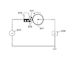
磁性キャリアの抵抗率ρ、比誘電率εの測定方法について説明する。図19は測定に用いた装置の概要図である。この装置は、キヤノン製複合機IRC-6800を改造したものを用いる。この複合機の感光ドラムを、感光層のないφ84mmのアルミニウム製の円筒体201(以下Alドラム)に置き換えて回転駆動可能とする。A1ドラムは周速が286mm/secの速さで回転する。そして改造機の現像器203内には、測定を行いたい磁性キャリア202を単体で充填する。そして、磁性キャリア202を担持したφ20mmの現像スリーブ231を、Alドラムに対向させる。この際、現像スリーブ231は、A1ドラムとの対向部においてA1ドラムと同じ方向に移動するように回転し、その周速は500mm/secである。なお、A1ドラムと現像スリーブとは、その対向部において300μmの空隙(SDギャップ)を形成するように位置決めされている。
磁性キャリアの抵抗率ρ、比誘電率εの測定方法について説明する。図19は測定に用いた装置の概要図である。この装置は、キヤノン製複合機IRC-6800を改造したものを用いる。この複合機の感光ドラムを、感光層のないφ84mmのアルミニウム製の円筒体201(以下Alドラム)に置き換えて回転駆動可能とする。A1ドラムは周速が286mm/secの速さで回転する。そして改造機の現像器203内には、測定を行いたい磁性キャリア202を単体で充填する。そして、磁性キャリア202を担持したφ20mmの現像スリーブ231を、Alドラムに対向させる。この際、現像スリーブ231は、A1ドラムとの対向部においてA1ドラムと同じ方向に移動するように回転し、その周速は500mm/secである。なお、A1ドラムと現像スリーブとは、その対向部において300μmの空隙(SDギャップ)を形成するように位置決めされている。
そして、上記の条件でAlドラム201及び現像スリーブ231を回転させながら、Alドラム201と現像スリーブ231間に電源204(NF社製 HVA4321)により、互いに電圧値が異なるAC電圧(Sin波)を各々印加する。このとき、この複数の電圧値は、キャリアのインピーダンスの電界依存性を調べたい電界範囲が得られる範囲内の値が適宜設定される。そして、この各電圧値におけるSin波において、周波数を1Hz~10KHzの間で変化させ、各印加電圧における応答電流を計測することにより、インピーダンスを測定することができる。本発明においては、英国ソーラトロン社製の誘電体測定システム205(126096W)により、この周波数変化は自動で行われ、インピーダンスの測定は自動で行われる。
解析方法について説明する。周波数を1Hzから10kHzまで変化させた際の各測定値(Re(Z)、Ima(Z))をプロットしたコール-コール(Cole-Cole)プロットより(図20参照)、等価回路を導出する。
Cole-Coleプロットが、図20のような半円の場合、磁性キャリアの等価回路がRCの並列回路であることを示唆している。そして、前記ソーラトロン社製の解析ソフト(Zview)により、RC並列回路でフィッティングすることにより、磁性キャリアのR成分、C成分を求めることができる。
Cole-Coleプロットが、図20のような半円の場合、磁性キャリアの等価回路がRCの並列回路であることを示唆している。そして、前記ソーラトロン社製の解析ソフト(Zview)により、RC並列回路でフィッティングすることにより、磁性キャリアのR成分、C成分を求めることができる。
なお、上記解析方法により求めた静電容量Ctには、現像スリーブ231とAlドラム201における現像領域(以下現像ニップ)外の空気層(比誘電率1)による影響も含まれる。つまり、磁性キャリア202の静電容量Cを求めるためには、上記解析方法により求められる静電容量Ctに対して、現像ニップ外の空気層による静電容量Caを引く必要がある。
Caの導出方法について説明する。磁性キャリア202を内包していない空の現像器203を上記測定方法により測定する。上記解析方法により求められるCatは、現像ニップ内の空気層による静電容量Canと現像ニップ外の空気層による静電容量Caの合成値となる。静電容量Canは、空気層の比誘電率(ε=1)とSDギャップ(cm)、磁性キャリアのAlドラム1に対する接触面積(cm2)から求めることができる。求められるCatとCanから、Caを導出することができる(Ca=Cat-Can)。最終的に、磁性キャリアの静電容量CはC=Ct-Caで決定される。
上記解析方法により求めた磁性キャリア202の抵抗Rと静電容量Cに対して、SDギャップ(cm)、磁性キャリア202のAlドラム201に対する接触面積(cm2)から、それぞれ磁性キャリア202の抵抗率ρ(Ω・cm)、比誘電率εを求めた。
なお、本出願の請求項における磁性キャリアの比誘電率ε、抵抗率ρは上記測定方法により求められた値を使用している。つまり、本請求項において使用される磁性キャリアの比誘電率ε、抵抗率ρは、磁性キャリア単体の物性値ではなく、現像ニップ内に存在する磁性キャリアと空気層を含めた比誘電率ε、抵抗率ρを表している。
また、上記測定方法により求められる抵抗率ρ、比誘電率εはトナーを考慮していない。実際にトナーと混合された2成分現像剤の各物性値は異なることが予想される。しかしながら、現像バイアス印加下においては、トナーは磁性キャリアと像担持体間を絶えず運動しているため、現像ニップ中の各物性値において、トナーの影響は小さいと考えられる。従って、本発明において、抵抗率ρ、誘電率εを規定するにあたり、トナーを考慮していない。
(5)磁性キャリアの抵抗率ρ、比誘電率εの電界強度依存性測定方法
磁性キャリアの抵抗率ρ、比誘電率εの電界強度依存性の測定方法について説明する。前述したように、図19の電源204により、印加されるSin波の振幅を変化させることにより、 抵抗率ρと比誘電率εの電界強度依存性を測定することができる。このとき、電界強度はSin波の振幅(V)をSDギャップ(cm)で割ったものである。
測定例を、図21(ρ)、図22(ε)に示す。Aは本実施例で使用した高誘電率キャリア、Bは本実施例で使用した低誘電率キャリア、Cは本実施例で使用した本発明に従うキャリアCである。
磁性キャリアの抵抗率ρ、比誘電率εの電界強度依存性の測定方法について説明する。前述したように、図19の電源204により、印加されるSin波の振幅を変化させることにより、 抵抗率ρと比誘電率εの電界強度依存性を測定することができる。このとき、電界強度はSin波の振幅(V)をSDギャップ(cm)で割ったものである。
測定例を、図21(ρ)、図22(ε)に示す。Aは本実施例で使用した高誘電率キャリア、Bは本実施例で使用した低誘電率キャリア、Cは本実施例で使用した本発明に従うキャリアCである。
(6)現像バイアス印加下における電界強度の決定方法
現像バイアス印加下における電界強度は次の通り決定される。
例えば、図7のような現像バイアスの場合、トナーを像担持体方向へ移動させる位相時間をT1とし、現像剤担持体方向へ移動させる位相時間をT2とする。磁性キャリアに拘束されたトナーに対し、画像部(VL)方向へ働く力が最も強く印加される電界強度はE1L(=(V1-VL)/SDギャップ)[V/cm]である。一方、像担持体上の非画像部(VD)のトナーに対し、現像剤担持体方向へ働く力が最も強く印加される電界強度は、電界強度E2D(=(V2-VD)/SDギャップ)[V/cm]である。現像バイアス印加下における磁性キャリアの抵抗率ρ、比誘電率εは、上記電界強度における抵抗率ρ、比誘電率εを測定方法(5)により求めた。
(7)実施例1
本実施例1では、物性値(ε、ρ)の異なる磁性キャリアにおいて、画像出力条件を固定の下、充電性、かぶりの測定を行なった。
検証結果について説明する。検討機は、前述したIRC-6800(キヤノン株式会社製のコピー複合機の型番)の改造機を用い、デジタル-イメージ露光方式、反転現像方式により現像を行なった。
本実施例1では、物性値(ε、ρ)の異なる磁性キャリアにおいて、画像出力条件を固定の下、充電性、かぶりの測定を行なった。
検証結果について説明する。検討機は、前述したIRC-6800(キヤノン株式会社製のコピー複合機の型番)の改造機を用い、デジタル-イメージ露光方式、反転現像方式により現像を行なった。
使用した像担持体は、膜厚dm=30μm、比誘電率εm=10、単位面積の静電容量C/S=3.0×10-6(F/m2)のα-Si感光体である。膜厚dm、単位面積当りの静電容量C/S、比誘電率εmは上記測定方法(2)により測定した。
上記像担持体は、図16に示す一次帯電器2によって、現像位置において、像担持体1表面を所望の暗電位VD(-480V)に均一に帯電し、スキャナー3により、現像位置において、ベタ部の電位を所望の明電位VL(-130V)に調整した。
現像スリーブ4cと像担持体1との距離(SDギャップ)は300μmである。
このとき使用した現像バイアスは、図7に示すようなDC成分にAC成分を重畳した波形である。具体的には、周波数5kHz、デューティ比60%、ピーク・ツウ・ピーク電圧(以下Vpp)が1.54kVのデューティ波である。
現像バイアスと明電位VL、暗電位VDとで決定される引き戻し方向と現像方向の電界強度E1L、E2D は、
E1L=3.7×10⁴ [V/cm]、E2D=2.6×104 [V/cm]であった。
DC成分のVdcは、像担持体の静電潜像、詳しくはベタ部に対応する明電位VL(-130V)、暗電位VD(-480V)に対して、必要な現像コントラスト(200V)、かぶり取り電位(150V)を確保する。そのために、Vdc=-330[V]で検討を行なった。ここで、現像コントラストとはVdcと明電位VLとの差であり、かぶり取り電位とはVdcと暗電位VDとの差である。
E1L=3.7×10⁴ [V/cm]、E2D=2.6×104 [V/cm]であった。
DC成分のVdcは、像担持体の静電潜像、詳しくはベタ部に対応する明電位VL(-130V)、暗電位VD(-480V)に対して、必要な現像コントラスト(200V)、かぶり取り電位(150V)を確保する。そのために、Vdc=-330[V]で検討を行なった。ここで、現像コントラストとはVdcと明電位VLとの差であり、かぶり取り電位とはVdcと暗電位VDとの差である。
なお、本検討において周波数は5kHzとしたが、周波数は3kHz~8kHzであることが好ましい。発明者らの検討によると、周波数が3kHzより小さい場合、どの条件においても、かぶりが許容レベルに達せず、周波数が8kHzより大きい場合、どの条件においても、充電性が許容レベルに達しないことがわかった。
次に、本発明で使用した現像剤について説明する。
現像剤としては非磁性トナーと磁性キャリアを有する2成分現像剤を使用している。使用した非磁性トナーとしては、従来公知の粉砕法により作成されたトナーを使用した。一方、使用した磁性キャリアとしては、物性値(ε、ρ)の異なる3種類のキャリアを用意した。それぞれの特徴を具体的に挙げる。
現像剤としては非磁性トナーと磁性キャリアを有する2成分現像剤を使用している。使用した非磁性トナーとしては、従来公知の粉砕法により作成されたトナーを使用した。一方、使用した磁性キャリアとしては、物性値(ε、ρ)の異なる3種類のキャリアを用意した。それぞれの特徴を具体的に挙げる。
・高誘電率(低抵抗)キャリアA:
高誘電率キャリアAとしては、例えば、コア材として下記式(1)又は(2)で表される磁性を有するマグネタイト及びフェライトを用いるものが挙げられる。
MO・Fe2O3 ・・・(1)
M・Fe2O4 ・・・(2)
(式中、Mは3価、2価又は1価の金属イオンを示す)
高誘電率キャリアAとしては、例えば、コア材として下記式(1)又は(2)で表される磁性を有するマグネタイト及びフェライトを用いるものが挙げられる。
MO・Fe2O3 ・・・(1)
M・Fe2O4 ・・・(2)
(式中、Mは3価、2価又は1価の金属イオンを示す)
Mとしては、Be,Mg、Ca、Rb、Sr、V、Cr、Mn、Fe、Co、Ni、Cu、Zn、Y、Zr、Nb、Mo、Cd、Pb及びLiが挙げられ、これらは単独或いは複数で用いることができる。
上記の磁性を有する金属化合物粒子の具体的化合物としては、例えば、Cu-Zn-Fe系フェライト、Mn-Mg-Fe系フェライト、Mn―Mg-Sr-Fe系フェライト及びLi-Fe系フェライトなどの鉄系酸化物が挙げられる。
フェライト粒子の製造方法としては、公知の方法を採用することができる。例えば、次のような方法を挙げることができる。
即ち、サブミクロンサイズに粉砕されたフェライト組成物に、バインダー、水、分散剤等を混合し、スプレードライヤー法や流動造粒法を用いて粒子を形成する。
その後、ロータリーキルンや回分式焼成炉で700~1400℃、好ましくは800~1300℃の範囲の温度で焼成する。次いで、篩分級して粒度分布を制御して、キャリア用の芯材粒子とする。
即ち、サブミクロンサイズに粉砕されたフェライト組成物に、バインダー、水、分散剤等を混合し、スプレードライヤー法や流動造粒法を用いて粒子を形成する。
その後、ロータリーキルンや回分式焼成炉で700~1400℃、好ましくは800~1300℃の範囲の温度で焼成する。次いで、篩分級して粒度分布を制御して、キャリア用の芯材粒子とする。
更にフェライト粒子表面に、浸漬法によりシリコーン樹脂等の樹脂を0.1~1.0質量%程度コートする。このようにして作製された磁性キャリアを、ここでは高誘電率キャリアAと呼ぶ。
・低誘電率(高抵抗)キャリアB:
低誘電率キャリアBとしては、例えば、次のようなものが挙げられる。
第一には、マグネタイト粒子と熱可塑性樹脂とを溶融混練し、粉砕して製造する磁性体分散型樹脂キャリアをコア材として用いるものである。
低誘電率キャリアBとしては、例えば、次のようなものが挙げられる。
第一には、マグネタイト粒子と熱可塑性樹脂とを溶融混練し、粉砕して製造する磁性体分散型樹脂キャリアをコア材として用いるものである。
第二には、マグネタイト粒子と熱可塑性樹脂とを溶媒中に溶融分散させたスラリーをスプレードライヤー等により噴霧乾燥させて製造する磁性体分散型樹脂キャリアをコア材として用いるものである。
第三には、マグネタイト粒子及びヘマタイト粒子存在下で、フェノールを直接重合により反応硬化させた磁性体分散型樹脂キャリアをコア材として用いるものである。
これらのキャリアコア材に、更に流動層コーティング装置などにより、熱可塑性樹脂等の樹脂を1.0~4.0質量%程度コートする。このようにして作製された磁性キャリアを、ここでは低誘電率キャリアBと呼ぶ。
・本発明に従うキャリアC:
一方、本発明に従うキャリアCとしては、例えば、ポーラス状のコアにシリコーン樹脂等の樹脂を流し込み、コア内の空隙を樹脂で充填したポーラス状樹脂充填キャリアを用いることができる。
一方、本発明に従うキャリアCとしては、例えば、ポーラス状のコアにシリコーン樹脂等の樹脂を流し込み、コア内の空隙を樹脂で充填したポーラス状樹脂充填キャリアを用いることができる。
キャリアCの作製方法としては、次のような方法を挙げることができる。
初めに、上記高誘電率キャリアAに用いられるようなNi、Cu、Zn、Li、Mg、Mn、Sr、Ca、Baからなる群から1種または2種以上選ばれる金属酸化物、酸化鉄(Fe2O3)を所定量秤量し、混合する。
初めに、上記高誘電率キャリアAに用いられるようなNi、Cu、Zn、Li、Mg、Mn、Sr、Ca、Baからなる群から1種または2種以上選ばれる金属酸化物、酸化鉄(Fe2O3)を所定量秤量し、混合する。
次に、得られた混合物を700~1000℃の範囲で5時間仮焼し、その後、0.3~3μm程度の粒径に粉砕する。得られた粉砕物に、バインダー、水、分散剤、必要に応じて有機微粒子やNa2CO3の如き空孔形成剤を加え、100~200℃の加熱雰囲気下でスプレードライヤーにより噴霧乾燥し、20~50μm程度の大きさに造粒する。
その後、酸素濃度5%以下の不活性ガス(例えば、N2ガス等)の雰囲気下において焼結温度800~1400℃で8~12時間焼成する。これにより、ポーラス状のコアが得られる。次いで、シリコーン樹脂を減圧した状態で浸漬法により8~15質量%充填し、180~220℃不活性ガス雰囲気下でそのシリコーン樹脂を硬化させる。また、必要な場合は、更に、浸漬法により、熱硬化性樹脂等の樹脂を0.1~5.0質量%程度被覆(コート)する。
上記製造方法において、コアのポーラス度、並びに、コア材の抵抗、更には、充填するシリコーン樹脂等の樹脂量、被覆樹脂であるコート樹脂の樹脂量等を制御することにより、キャリアの比誘電率ε、抵抗率ρを制御することができる。
次に、このようなキャリアを用いた画像形成装置において、充電性やかぶりを改善するべく、発明者らが行った検討結果を、以下に示していく。
まず、充電率を改善するための有効な手段として、振動電圧による現像バイアスによりトナー運動を制御する方法を検討した。具体的には、図7に示すように、1周期に対してトナーに対して現像剤担持体から像担持体方向に向かう第1の方向の静電気力を生じさせる位相時間をT1、T1におけるピーク電圧を第1のピーク電圧V1とする。また、トナーに対して像担持体から現像剤担持体方向に向かう第2の方向の静電気力を生じさせる位相時間をT2、T2におけるピーク電圧を第2のピーク電圧V2とし、V1とV2を交互に繰り返す。そのとき、現像バイアスのDC成分Vdcや現像方向のピーク電圧V1をある電圧値に維持したまま、1周期に占めるT2の割合(以下デューティ(Duty)比という)を上げる。この際、周期T1におけるVdcを基準軸としたと波形の積分値と、周期T2におけるVdcを基準軸とした波形の積分値とが、同じ値となるように、V1とV2の値、及びT1とT2の割合が決定される。これにより、引き戻し方向のピーク電圧V2を弱める振動バイアス(以下デューティ(Duty)波という)とする。なお、ここでのデューティ比(Du)(%)は、(T2/(T1+T2))×100 という関係式で算出されるものである。
まず、充電率を改善するための有効な手段として、振動電圧による現像バイアスによりトナー運動を制御する方法を検討した。具体的には、図7に示すように、1周期に対してトナーに対して現像剤担持体から像担持体方向に向かう第1の方向の静電気力を生じさせる位相時間をT1、T1におけるピーク電圧を第1のピーク電圧V1とする。また、トナーに対して像担持体から現像剤担持体方向に向かう第2の方向の静電気力を生じさせる位相時間をT2、T2におけるピーク電圧を第2のピーク電圧V2とし、V1とV2を交互に繰り返す。そのとき、現像バイアスのDC成分Vdcや現像方向のピーク電圧V1をある電圧値に維持したまま、1周期に占めるT2の割合(以下デューティ(Duty)比という)を上げる。この際、周期T1におけるVdcを基準軸としたと波形の積分値と、周期T2におけるVdcを基準軸とした波形の積分値とが、同じ値となるように、V1とV2の値、及びT1とT2の割合が決定される。これにより、引き戻し方向のピーク電圧V2を弱める振動バイアス(以下デューティ(Duty)波という)とする。なお、ここでのデューティ比(Du)(%)は、(T2/(T1+T2))×100 という関係式で算出されるものである。
このようなデューティ波は、位相時間T2において、トナーを現像剤担持体方向へ引き戻す力を弱めるために、トナーが像担持体近傍に局在する。これにより、最終的に像担持体上に現像されるトナー量が増加し、充電不良が改善される。
図8は、キャリアAを用いて上記デューティ波のデューティ比Duを可変した際に、充電性の変化を示した図である。上記理由により、デューティ比Duを上げるに伴い、矩形波(デューティ比50%)に比べて、充電性は飛躍的に改善される。しかし、デューティ比が80%を超えると、トナーを像担持体方向へ移動させる時間に対し、現像剤担持体方向へ移動させる位相時間が長くなり過ぎ、結果的にトナーを像担持体方向へ移動させることができなくなり、充電性は大きく減少してしまう。なおこの特性については、図12のようにキャリアの種類を変更して検討しても、同様な傾向の結果が得られた。
よって発明者らの検討結果によれば、キャリアの種類や現像バイアスの周波数によらず、デューティ比Duが60%から80%のときに、矩形波に比べて十分優位性が得られることがわかった。
ところで、デューティ波のようにピーク電圧V2を弱めれば、当然ながら非画像部へのトナー付着(以下かぶり)が悪化してしまう。また、発明者らの検討によれば、高静電容量の像担持体は低静電容量の像担持体に比べて、弱帯電したトナーが、強い鏡映力により非画像部に付着しやすくなるため、かぶりが悪化し易いことがわかった。
図9は、キャリアAを用いかつα-Si感光体を備えた画像形成装置に対し、デューティ波のデューティ比Duを可変した際の、かぶりの変化を示した図である。
図に示した通り、デューティ比Duを上げるに伴い、かぶりは飛躍的に悪化してしまうことがわかった。ここでかぶりの数値化は、以下の方法を用いた。画像白地部(非画像部)の反射濃度Dsをマクベス社製の反射濃度計(SERISE1200)により測定する。一方、紙自身の反射濃度Drを同様に測定し、かぶり濃度を、かぶり濃度(%)=Dr-Dsとした。
図に示した通り、デューティ比Duを上げるに伴い、かぶりは飛躍的に悪化してしまうことがわかった。ここでかぶりの数値化は、以下の方法を用いた。画像白地部(非画像部)の反射濃度Dsをマクベス社製の反射濃度計(SERISE1200)により測定する。一方、紙自身の反射濃度Drを同様に測定し、かぶり濃度を、かぶり濃度(%)=Dr-Dsとした。
以上のように、高静電容量の像担持体に対し、デューティ波により充電不良は著しく改善されるものの、このデューティ波だけでは、かぶりとの両立が困難であった。
そこで、充電効率の向上が望めるデューティ波を使用する際に、かぶりを改善するための方法について、発明者らは更なる検討を行った。その中でも有効な手段として、使用する磁性キャリアの抵抗を高抵抗化する方法を見出した。
図10はα-Si感光体に対し、使用する磁性キャリアの抵抗を可変した際のかぶりとデューティ比Duの関係である。図10において低抵抗キャリアは上述のキャリアAであり、高抵抗キャリアは上述のキャリアBである。図10の通り、磁性キャリアの抵抗を高抵抗化することにより、かぶりは飛躍的に改善されることが判明した。
図10はα-Si感光体に対し、使用する磁性キャリアの抵抗を可変した際のかぶりとデューティ比Duの関係である。図10において低抵抗キャリアは上述のキャリアAであり、高抵抗キャリアは上述のキャリアBである。図10の通り、磁性キャリアの抵抗を高抵抗化することにより、かぶりは飛躍的に改善されることが判明した。
かぶりが改善される理由は、以下のように考えられる。
磁性キャリアは一般的に、抵抗成分Rと容量成分CからなるRC並列回路とみなすことができる。磁性キャリアがトナーと摩擦帯電することにより、磁性キャリアの容量成分にはトナー電荷と逆極性の電荷Qc(以下カウンターチャージ)が蓄えられる。このとき、カウンターチャージは式2のように、ερの時定数で減衰すると考えられる。
磁性キャリアは一般的に、抵抗成分Rと容量成分CからなるRC並列回路とみなすことができる。磁性キャリアがトナーと摩擦帯電することにより、磁性キャリアの容量成分にはトナー電荷と逆極性の電荷Qc(以下カウンターチャージ)が蓄えられる。このとき、カウンターチャージは式2のように、ερの時定数で減衰すると考えられる。
本発明者らの検討によると、かぶりは、トナーを現像剤担持体に移動させる位相での電界強度E2Dにおける磁性キャリアの、比誘電率ε,抵抗率ρにより表される電荷減衰の時定数ε0 ε ρ(s)と電界強度E2Dの積に相関があることが確認された。
図11はε0 ε ρ E2D(s・V/cm)に対するかぶりの関係である。図11の通り、ε0ερE2Dの増加に伴い、かぶりは改善され、20 ≦ε0 ε ρ E2D(s・V/cm)のとき、かぶりは許容レベル(2%以下)に達することが確認された。なお、ε0 ε ρ E2Dの値が大きいほどカウンターチャージ保持能力が高くなり、かぶり防止にはより有効となるので、かぶり防止という観点だけから言えば、ε0 ε ρ E2Dの値に上限はない。
図11はε0 ε ρ E2D(s・V/cm)に対するかぶりの関係である。図11の通り、ε0ερE2Dの増加に伴い、かぶりは改善され、20 ≦ε0 ε ρ E2D(s・V/cm)のとき、かぶりは許容レベル(2%以下)に達することが確認された。なお、ε0 ε ρ E2Dの値が大きいほどカウンターチャージ保持能力が高くなり、かぶり防止にはより有効となるので、かぶり防止という観点だけから言えば、ε0 ε ρ E2Dの値に上限はない。
この理由は次のように考えられる。
磁性キャリアが非画像部に付着した弱帯電したかぶりトナーを捕集するために、必要なカウンターチャージをqとする。このとき、磁性キャリアがq以上の電荷を有す時間tは、式2から、t=-ε0 ε ρ log(q’)となる。但し、q’=q/Q0 である。
磁性キャリアが非画像部に付着した弱帯電したかぶりトナーを捕集するために、必要なカウンターチャージをqとする。このとき、磁性キャリアがq以上の電荷を有す時間tは、式2から、t=-ε0 ε ρ log(q’)となる。但し、q’=q/Q0 である。
かぶりレベルは、この時間tと、現像剤担持体方向へ移動させる電界強度E2Dに起因していると考えられる。以上の理由により、かぶりとε0 ε ρ E2Dは相関関係にあると考えられる。
磁性キャリアの抵抗(ρ)を高抵抗化することによりかぶりが改善した理由は、磁性キャリアのε0ερが増加し、必要なカウンターチャージを保持する時間が長くなったためと考えられる。この残留したカウンターチャージにより、非画像部に付着した弱帯電したかぶりトナーを捕集し、かぶりが改善されたと考えられる。
しかし、発明者らの検討によれば、かぶり改善を狙って単純に磁性キャリアを高抵抗化するだけでは、充電性が悪化することが判明した。図12は、磁性キャリアの抵抗を可変した際の充電性とデューティ比の関係である。図12の通り、磁性キャリアの抵抗を高抵抗化することにより、充電性は悪化する。図13は、上記で用いた高抵抗キャリア、低抵抗キャリアにおける抵抗率の電界強度依存性である。電界強度増大に伴い、抵抗率は減少する。
一方、図14は、これら磁性キャリアにおける比誘電率の電界強度依存性である。一般的に磁性キャリアを高抵抗化した場合、それに伴い磁性キャリアの比誘電率は減少する。
図15は、抵抗率ρと比誘電率εから求められるε0 ε ρ(s)と、電界強度の関係である。磁性キャリアを高抵抗化すると充電性が悪化する理由は上記物性値から以下のように説明できる。
磁性キャリアを高抵抗化することにより、ε0 ε ρ(s)が増大し、磁性キャリアにはカウンターチャージが残留し易くなる。このため、トナーが磁性キャリアのカウンターチャージにより、磁性キャリアに引き戻され、結果的に充電性が悪化すると考えられる。
また、本発明者らの検討によると、比誘電率自身が充電性に影響を及ぼすことが確認されている。具体的には、比誘電率の小さい磁性キャリアは大きい磁性キャリアに比べて、充電性が低い。これは現像スリーブと像担持体を平行平板に見立てて説明することができる。
平行平板に電圧を印加した場合、平行平板内の電場は一様になる。一方、平行平板内に誘電体を入れた場合、境界条件から平行平板内の誘電体周辺の場は大きく歪むことになる。このため、誘電体の誘電率が増加するに伴い、等電位面から求められる誘電体周辺に加わる電場は増加する。
つまり、現像スリーブと像担持体間に磁性キャリアがあるとき、磁性キャリアの誘電率が大きいほど、磁性キャリア周辺に加わる電場は大きくなり、トナーが磁性キャリアから飛翔し易くなる。一方、誘電率が小さい場合、トナーが磁性キャリアから飛翔し難くなり、結果的に充電性が悪化すると考えられる。
上記の通り、かぶりの抑制を目的として磁性キャリアを高抵抗化すると、カウンターチャージ、及び誘電率による電場の影響を受けて充電性が悪化するものと考えられる。
以上のように、デューティバイアスを用いる画像形成装置において、単にキャリアAやキャリアBを用いるだけでは、高静電容量の像担持体において、かぶりと充電性を両立することは難しい。
そこで、本発明者らが鋭意検討した結果、先述のキャリアCとデューティバイアスとを、所定の条件下で用いることで、かぶりと充電性の両立を図れる構成を見出す事に成功した。
以上のように、デューティバイアスを用いる画像形成装置において、単にキャリアAやキャリアBを用いるだけでは、高静電容量の像担持体において、かぶりと充電性を両立することは難しい。
そこで、本発明者らが鋭意検討した結果、先述のキャリアCとデューティバイアスとを、所定の条件下で用いることで、かぶりと充電性の両立を図れる構成を見出す事に成功した。
高誘電率キャリアA、低誘電率キャリアB、本発明に従うキャリアCの抵抗率ρと比誘電率εの電界強度依存性の測定結果を図21、22に示す。
高誘電率キャリアAは、電界強度増加に伴い、抵抗率ρが減少し、比誘電率εが増加した。低誘電率キャリアBは電界強度増加に伴い、抵抗率ρ、比誘電率εともに、変化が非常に小さい。一方、本発明に従うキャリアCは、所定の電界強度付近、この例では電界強度2.6×10⁴(V/cm)付近までは、電界強度増加に伴う変化率が小さい。しかし、電界強度2.6×104(V/cm)付近を過ぎると、電界強度増加に伴い、抵抗率ρの減少度合い(減少率)が大きくなり、抵抗率ρは急激に減少し、比誘電率εの増加度合い(増加率)は大きくなり、比誘電率εは急激に増加した。
よってキャリアCは、所定の電界強度よりも大きい電界強度における電界強度の変化に対する抵抗率の減少率が、前記所定の電界強度よりも小さい電界強度における電界強度の変化に対する抵抗率の減少率よりも大きい特性を有する。更にキャリアCは、所定の電界強度よりも大きい電界強度における電界強度の変化に対する比誘電率の増加率が、前記所定の電界強度よりも小さい電界強度における電界強度の変化に対する比誘電率の増加率よりも大きい特性を有する。
上記物性値の変化は、次のような原因だと考えられる。
例えば、高誘電率キャリアAのように、コア材が導電性の材料で形成された磁性キャリアの場合、電圧が印加された際、磁性キャリア内、及び磁性キャリア間で電気的なパスが出来やすい。電界強度増加に伴い、電気物性値(ε、ρ)が変化すると考えられる。一方、本発明に従うキャリアCの場合、コアが導電性の材料で形成されたポーラス構造であり、且つ、その中を絶縁性の樹脂を充填しているために、コア内部は絶縁性の樹脂部と導電性のポーラス部が存在する。
例えば、高誘電率キャリアAのように、コア材が導電性の材料で形成された磁性キャリアの場合、電圧が印加された際、磁性キャリア内、及び磁性キャリア間で電気的なパスが出来やすい。電界強度増加に伴い、電気物性値(ε、ρ)が変化すると考えられる。一方、本発明に従うキャリアCの場合、コアが導電性の材料で形成されたポーラス構造であり、且つ、その中を絶縁性の樹脂を充填しているために、コア内部は絶縁性の樹脂部と導電性のポーラス部が存在する。
ここで、絶縁性の樹脂部や導電性のポーラス部との境界において、電荷の流れをある程度遮断することができると考えられる。しかし、遮断できる限界値(この場合、電界強度2.6×10⁴(V/cm))を超えると、コアの導電性部により、急激な電気物性値(ε、ρ)の変化が起きると考えられる。前述の通り、コアのポーラス度、並びに、コア材の抵抗、更には、充填するシリコーン樹脂等の樹脂量、コート樹脂の樹脂量等を制御することにより、磁性キャリアの比誘電率ε、抵抗率ρを制御することができる。また、上記の限界値を制御することも可能となる。
この例では、引き戻し方向の電界強度E2Dは2.6×10⁴(V/cm)であり、この付近までは、抵抗率ρは大きく、比誘電率εは小さい特性を有する。現像方向の電解強度E1Lは、3.7×104 [V/cm]であり、特性の変化が大きい領域で、抵抗率ρは低抵抗のキャリアAと同等にまで大きく低下し、比誘電率εは急激に高くなって、高誘電率キャリアAの比誘電率を大きく超えた値となっている。
この例では、引き戻し方向の電界強度E2Dは2.6×10⁴(V/cm)であり、この付近までは、抵抗率ρは大きく、比誘電率εは小さい特性を有する。現像方向の電解強度E1Lは、3.7×104 [V/cm]であり、特性の変化が大きい領域で、抵抗率ρは低抵抗のキャリアAと同等にまで大きく低下し、比誘電率εは急激に高くなって、高誘電率キャリアAの比誘電率を大きく超えた値となっている。
本発明で使用した2成分現像剤は、トナーの摩擦帯電量が等しくなるように調整した。具体的には、上記非磁性トナーと磁性キャリアの混合比を可変した。実際に、全重量に対する非磁性トナーの重量%は8%~10%であった。また、このとき、トナーの摩擦帯電量(以下Q/M)は約-50μC/gであった。
ここで、使用したQ/Mの実測方法について説明する。
図23に示したファラデーゲージ300は、軸径の異なる金属製の内筒301と外筒302を同軸になるように配置した2重筒と、内筒301内に更にトナーを取り入れるためのフィルター303を備えている。内筒301と外筒302間は絶縁部材302によって絶縁されている。エアー吸引により、像担持体上のトナーをフィルター303内に取り込むことにより、内筒301と外筒302が絶縁されているために、トナーの電荷量Qによる静電誘導を引き起こす。
図23に示したファラデーゲージ300は、軸径の異なる金属製の内筒301と外筒302を同軸になるように配置した2重筒と、内筒301内に更にトナーを取り入れるためのフィルター303を備えている。内筒301と外筒302間は絶縁部材302によって絶縁されている。エアー吸引により、像担持体上のトナーをフィルター303内に取り込むことにより、内筒301と外筒302が絶縁されているために、トナーの電荷量Qによる静電誘導を引き起こす。
この誘起された電荷量Qを測定し、内筒301内のトナー重量Mで割った値をQ/M(μC/g)とした。測定は、ケースレーインスツルメンツ株式会社製の計測器「KEITHLEY 616 DIGITAL ELECTROMETER」を使用した。
表1には、以上の条件下において、高誘電率キャリアA、低誘電率キャリアB、本発明に従うキャリアCを使った際の各充電率、かぶり評価の結果を示す。
表1には、以上の条件下において、高誘電率キャリアA、低誘電率キャリアB、本発明に従うキャリアCを使った際の各充電率、かぶり評価の結果を示す。
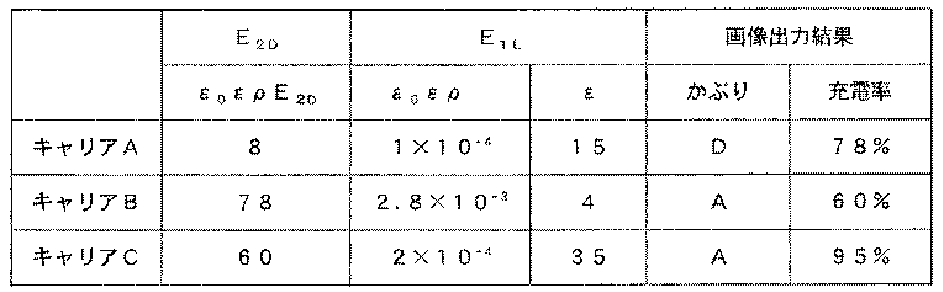
ここでかぶり評価方法について説明する。画像白地部の反射濃度Dsをマクベス社製の反射濃度計(SERISE1200)により測定する。一方、紙自身の反射濃度Drを同様に測定し、かぶり濃度を以下のように決定した。
かぶり濃度(%)=Dr-Ds
求めたかぶり濃度に対して、下記の評価基準に従って評価した。
A:0.5%以下・・・非常に良い
B:0.6~1%以下・・・良い
C:1~2.0%以下・・・許容レベル
D:2%~・・・悪い
求めたかぶり濃度に対して、下記の評価基準に従って評価した。
A:0.5%以下・・・非常に良い
B:0.6~1%以下・・・良い
C:1~2.0%以下・・・許容レベル
D:2%~・・・悪い
表1に示されるように、充電率、かぶりを両立する磁性キャリアは本発明に従うキャリアCのみであった。
(8)実施例2
本実施例2では、キャリア物性値(ε、ρ)と充電率、かぶりの関係を明確にするために、実施例1に磁性キャリアD~Hを加えて検討を行なった。キャリアD~HはキャリアCと同様の製造方法で作成した。このとき、コアのポーラス度、並びに、コア材の抵抗、更には、充填するシリコーン樹脂等の樹脂量、コート樹脂の樹脂量等を制御することにより、キャリアの比誘電率ε、抵抗率ρを下記のように制御した。磁性キャリアA~Hの物性値(ε、ε0 ε ρ)、かぶり、充電率の測定結果は以下のとおりである。真空の誘電率ε0は定数である。
本実施例2では、キャリア物性値(ε、ρ)と充電率、かぶりの関係を明確にするために、実施例1に磁性キャリアD~Hを加えて検討を行なった。キャリアD~HはキャリアCと同様の製造方法で作成した。このとき、コアのポーラス度、並びに、コア材の抵抗、更には、充填するシリコーン樹脂等の樹脂量、コート樹脂の樹脂量等を制御することにより、キャリアの比誘電率ε、抵抗率ρを下記のように制御した。磁性キャリアA~Hの物性値(ε、ε0 ε ρ)、かぶり、充電率の測定結果は以下のとおりである。真空の誘電率ε0は定数である。

表2に示される通り、かぶりが許容レベルであり、且つ充電率が90%以上を両立する磁性キャリアは、キャリアC、D、Eであった。
理由は以下のように考えられる。本条件において、かぶりの許容レベルを満たす磁性キャリアは、キャリアB、C、D、E、G、Hであった。
これらの磁性キャリアは電界強度E2D(V/cm)において、
20 ≦ε0 ε ρ E2D(s・V/cm)
を満たす。
理由は以下のように考えられる。本条件において、かぶりの許容レベルを満たす磁性キャリアは、キャリアB、C、D、E、G、Hであった。
これらの磁性キャリアは電界強度E2D(V/cm)において、
20 ≦ε0 ε ρ E2D(s・V/cm)
を満たす。
このため、非画像部(VD)に対し、現像バイアスのトナーを現像剤担持体方向へ移動させる位相時間T2で決定される電界強度E2D において、磁性キャリアに残留するカウンターチャージが十分大きい。このカウンターチャージにより、非画像部に付着したかぶりトナーを回収することができる。
次に、本条件において、充電率の許容レベルを満たすキャリアは、キャリアC、D、E、Fであった。これらのキャリアは電界強度E1L(V/cm)において、 ε0ερ(s)≦6.0×10⁻⁴ 且つ 30 ≦ ε を満たす。このため、画像部(VL)に対し、現像バイアスのトナーを像担持体方向へ移動させる位相時間T1で印加される電界強度E1L において、磁性キャリアに残留するカウンターチャージが十分小さい。
このように時定数ε0ερ(s)を6.0×10⁻⁴ 以下とすることで、カウンターチャージが消失し易い状態になり、カウンターチャージによるトナー飛翔運動の阻害を防止できる。これにより、画像部での充電性を向上させることができる。また、磁性キャリアの比誘電率εを30以上と大きな値にするため、磁性キャリア周辺に加わる電場が大きくなり、トナーが磁性キャリアから飛翔し易くなる。なお、比誘電率εの値については、大きいほど電場が大きくなり飛翔が促進されることになる為、充電不良の改善という観点だけから言えば比誘電率εの値に上限はない。以上により、本発明に従うキャリアC、D、Eのみが、本願請求項1の範囲を満たす。
(9)実施例3
実施例2の電界強度E1Lを3.7×10⁴ [V/cm]で固定したまま、E2D を可変するために、デューティ比、Vppをそれぞれ、70%、1.33kVに代えて同様の検討を行った。
実施例2の電界強度E1Lを3.7×10⁴ [V/cm]で固定したまま、E2D を可変するために、デューティ比、Vppをそれぞれ、70%、1.33kVに代えて同様の検討を行った。
具体的には、周波数5kHz、デューティ比70%、Vpp1.33kVのデューティ波である。現像バイアスと明電位VL、暗電位VDとで決定される電界強度E1L、E2D は、E1L=3.7×10⁴ [V/cm]、E2D=1.9×104 [V/cm]であった。
表3に、このときの磁性キャリアA~Gの物性値(ε、ε0ερ)、かぶり、充電率の測定結果を示している。
表3に、このときの磁性キャリアA~Gの物性値(ε、ε0ερ)、かぶり、充電率の測定結果を示している。
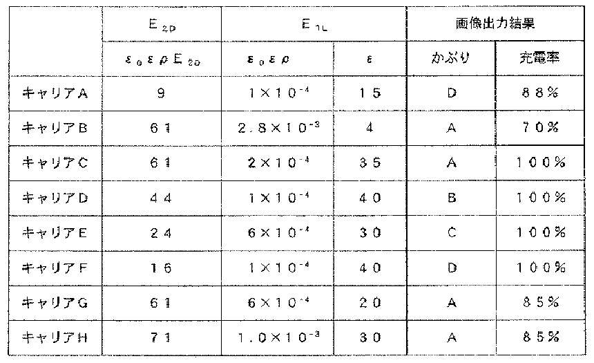
表3に示す通り、かぶりが許容レベルであり、且つ充電率が90%以上を両立する磁性キャリアは、キャリアC、D、Eであった。
理由は以下のように考えられる。本条件において、かぶりの許容レベルを満たす磁性キャリアは、キャリアB、C、D、E、G、Hであった。これらの磁性キャリアは電界強度E2D(V/cm)において、20 ≦ε0 ε ρ E2D[s・V/cm]を満たす。このため、非画像部(VD)に対し、現像バイアスのトナーを現像剤担持体方向へ移動させる位相時間T2で決定される電界強度E2D において、磁性キャリアに残留するカウンターチャージが十分大きい。このカウンターチャージにより、非画像部に付着したかぶりトナーを回収することができる。
次に、本条件において、充電率の許容レベルを満たすキャリアは、キャリアC、D、E、Fであった。これらのキャリアは、電界強度E1L(V/cm)において、 ε0ερ(s)≦6.0×10⁻⁴ 且つ、30 ≦ ε を満たす。このため、画像部(VL)に対し、現像バイアスのトナーを像担持体方向へ移動させる位相時間T1で印加される電界強度E1L において、磁性キャリアに残留するカウンターチャージが十分小さい。カウンターチャージにより、トナーの運動を阻害し、充電性を悪化させることを軽減することができる。また、磁性キャリアの比誘電率εが十分大きいため、磁性キャリア周辺に加わる電場が大きくなり、トナーが磁性キャリアから飛翔し易くなる。
以上により、本発明に従うキャリアC、D、Eのみが、本請求項1の範囲を満たす。
以上により、本発明に従うキャリアC、D、Eのみが、本請求項1の範囲を満たす。
(10)実施例4
実施例2の電界強度E1Lを3.7×10⁴ [V/cm]で固定したまま、E2D を可変するために、デューティ比、Vppをそれぞれ、80%、1.16kVに代えて同様の検討を行った。具体的には、周波数5kHz、デューティ比80%、Vpp1.16kVのデューティ波である。現像バイアスと明電位VL、暗電位VDとで決定される電界強度E1L、E2D は、
E1L=3.7×10⁴ [V/cm]、
E2D=1.4×10⁴ [V/cm]、であった。
このとき、磁性キャリアA~Gの物性値(ε、ε0 ε ρ)、かぶり、充電率の測定結果は以下の通りである。
実施例2の電界強度E1Lを3.7×10⁴ [V/cm]で固定したまま、E2D を可変するために、デューティ比、Vppをそれぞれ、80%、1.16kVに代えて同様の検討を行った。具体的には、周波数5kHz、デューティ比80%、Vpp1.16kVのデューティ波である。現像バイアスと明電位VL、暗電位VDとで決定される電界強度E1L、E2D は、
E1L=3.7×10⁴ [V/cm]、
E2D=1.4×10⁴ [V/cm]、であった。
このとき、磁性キャリアA~Gの物性値(ε、ε0 ε ρ)、かぶり、充電率の測定結果は以下の通りである。
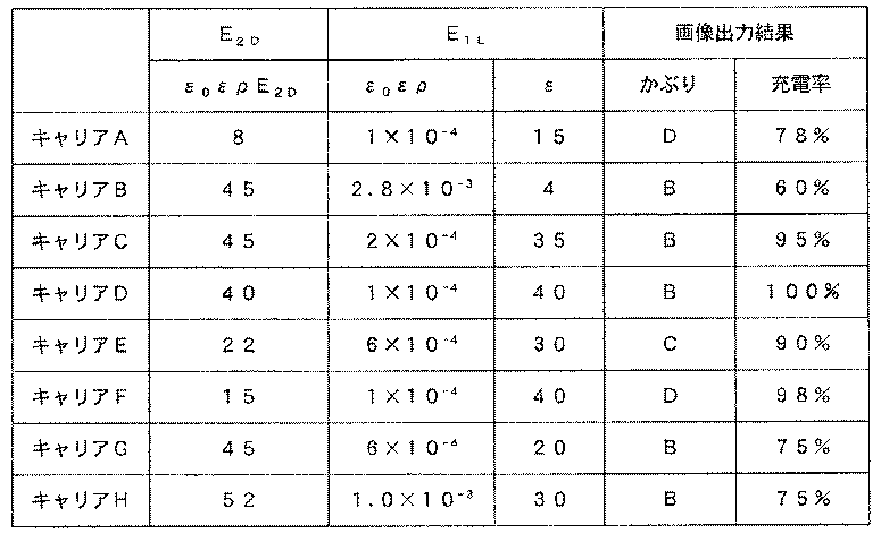
かぶりが許容レベルであり、且つ充電率が90%以上を両立する磁性キャリアは、キャリアC、D、Eであった。
理由は以下のように考えられる。本条件において、かぶりの許容レベルを満たす磁性キャリアは、キャリアB、C、D、E、G、Hであった。これらの磁性キャリアは電界強度E2D(V/cm)において、
20 ≦ε0 ε ρ E2D(s・V/cm)
を満たす。
20 ≦ε0 ε ρ E2D(s・V/cm)
を満たす。
このため、非画像部(VD)に対し、現像バイアスのトナーを現像剤担持体方向へ移動させる位相時間T2で決定される電界強度E2D において、磁性キャリアに残留するカウンターチャージが十分大きい。このため、このカウンターチャージにより、非画像部に付着したかぶりトナーを回収することができる。
次に、本条件において、充電率の許容レベルを満たすキャリアは、キャリアC、D、E、Fであった。これらのキャリアは電界強度E1L(V/cm)において、 ε0ερ(s)≦6.0×10⁻⁴ 且つ 30 ≦ ε
を満たす。
を満たす。
このため、画像部(VL)に対し、現像バイアスのトナーを像担持体方向へ移動させる位相時間T1で印加される電界強度E1L において、磁性キャリアに残留するカウンターチャージが十分小さい。したがって、カウンターチャージにより、トナーの運動を阻害し、充電性を悪化させることを軽減することができる。また、磁性キャリアの比誘電率εが十分大きいため、磁性キャリア周辺に加わる電場が大きくなり、トナーが磁性キャリアから飛翔し易くなる。
以上により、本発明に従うキャリアC、D、Eのみが、本請求項1の範囲を満たす。
(11)実施例5
実施例2の電界強度E1Lを可変するために、デューティ比、Vppをそれぞれ、60%、0.85kVに代えて同様の検討を行った。具体的には、周波数5kHz、デューティ比60%、Vpp0.85kVのデューティ波である。現像バイアスと明電位VL、暗電位VDとで決定される電界強度E1L、E2D は、E1L=2.3×10⁴ (V/cm)、E2D=1.6×104 (V/cm)であった。このときの、磁性キャリアI~Lの物性値(ε、ε0 ε ρ)、かぶり、充電率の測定結果は、表5に示すとおりである。キャリアI~LもキャリアCと同様の製造方法で作成した。
実施例2の電界強度E1Lを可変するために、デューティ比、Vppをそれぞれ、60%、0.85kVに代えて同様の検討を行った。具体的には、周波数5kHz、デューティ比60%、Vpp0.85kVのデューティ波である。現像バイアスと明電位VL、暗電位VDとで決定される電界強度E1L、E2D は、E1L=2.3×10⁴ (V/cm)、E2D=1.6×104 (V/cm)であった。このときの、磁性キャリアI~Lの物性値(ε、ε0 ε ρ)、かぶり、充電率の測定結果は、表5に示すとおりである。キャリアI~LもキャリアCと同様の製造方法で作成した。
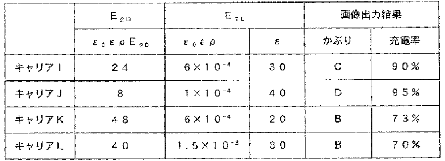
かぶりが許容レベルであり、且つ充電率が90%以上を両立する磁性キャリアは、キャリアIであった。
理由は以下のように考えられる。本条件において、かぶりの許容レベルを満たす磁性キャリアは、キャリアI、K、Lであった。これらの磁性キャリアは、電界強度E2D(V/cm)において、
20 ≦ε0 ε ρ E2D(s・V/cm)
を満たす。
20 ≦ε0 ε ρ E2D(s・V/cm)
を満たす。
このため、非画像部(VD)に対し、現像バイアスのトナーを現像剤担持体方向へ移動させる位相時間T2で決定される電界強度E2D において、磁性キャリアに残留するカウンターチャージが十分大きい。したがって、このカウンターチャージにより、非画像部に付着したかぶりトナーを回収することができる。
次に、本条件において、充電率の許容レベルを満たすキャリアは、キャリアI、Jであった。これらのキャリアは電界強度E1L(V/cm)において、
ε0ερ(s)≦6.0×10⁻⁴ 且つ 30 ≦ ε を満たす。
ε0ερ(s)≦6.0×10⁻⁴ 且つ 30 ≦ ε を満たす。
このため、画像部(VL)に対し、現像バイアスのトナーを像担持体方向へ移動させる位相時間T1で印加される電界強度E1L において、磁性キャリアに残留するカウンターチャージが十分小さい。したがって、カウンターチャージにより、トナーの運動を阻害し、充電性を悪化させることを軽減することができる。また、磁性キャリアの比誘電率εが十分大きいため、磁性キャリア周辺に加わる電場が大きくなり、トナーが磁性キャリアから飛翔し易くなる。
以上により、本発明に従うキャリアIのみが、本請求項1の範囲を満たす。
以上により、本発明に従うキャリアIのみが、本請求項1の範囲を満たす。
(12)実施例6
実施例5の電界強度E1Lを2.3×10⁴ (V/cm)で固定したまま、E2D を可変するために、デューティ比、Vppをそれぞれ、70%、0.74kVに代えて同様の検討を行った。
実施例5の電界強度E1Lを2.3×10⁴ (V/cm)で固定したまま、E2D を可変するために、デューティ比、Vppをそれぞれ、70%、0.74kVに代えて同様の検討を行った。
具体的には、周波数5kHz、デューティ比70%、Vpp0.74kVのデューティ波である。現像バイアスと明電位VL、暗電位VDとで決定される電界強度E1L、E2D は、
E1L=2.3×10⁴ (V/cm)
E2D=1.3×10⁴ (V/cm)
であった。
E1L=2.3×10⁴ (V/cm)
E2D=1.3×10⁴ (V/cm)
であった。
このとき、磁性キャリアI~Lの物性値(ε、ε0 ε ρ)、かぶり、充電率の測定結果は表6に示す通りである。

表6に示される通り、かぶりが許容レベルであり、且つ充電率が90%以上を両立する磁性キャリアは、キャリアIであった。
理由は以下のように考えられる。本条件において、かぶりの許容レベルを満たす磁性キャリアは、キャリアI、K、Lであった。これらの磁性キャリアは電界強度E2D(V/cm)において、
20 ≦ε0 ε ρ E2D(s・V/cm)
を満たす。このため、非画像部(VD)に対し、現像バイアスのトナーを現像剤担持体方向へ移動させる位相時間T2で決定される電界強度E2D において、磁性キャリアに残留するカウンターチャージが十分大きい。したがって、このカウンターチャージにより、非画像部に付着したかぶりトナーを回収することができる。
20 ≦ε0 ε ρ E2D(s・V/cm)
を満たす。このため、非画像部(VD)に対し、現像バイアスのトナーを現像剤担持体方向へ移動させる位相時間T2で決定される電界強度E2D において、磁性キャリアに残留するカウンターチャージが十分大きい。したがって、このカウンターチャージにより、非画像部に付着したかぶりトナーを回収することができる。
次に、本条件において、充電率の許容レベルを満たすキャリアは、キャリアI、Jであった。これらのキャリアは、電界強度E1L(V/cm)において、
ε0ερ(s)≦6.0×10⁻⁴ 且つ 30 ≦ ε
を満たす。
ε0ερ(s)≦6.0×10⁻⁴ 且つ 30 ≦ ε
を満たす。
このため、画像部(VL)に対し、現像バイアスのトナーを像担持体方向へ移動させる位相時間T1で印加される電界強度E1L において、磁性キャリアに残留するカウンターチャージが十分小さい。したがって、カウンターチャージにより、トナーの運動を阻害し、充電性を悪化させることを軽減することができる。また、磁性キャリアの比誘電率εが十分大きいため、磁性キャリア周辺に加わる電場が大きくなり、トナーが磁性キャリアから飛翔し易くなる。以上により、本発明に従うキャリアIのみが、本請求項1の範囲を満たす。
(13)実施例7
実施例5の電界強度E1Lを2.3×10⁴ (V/cm)で固定したまま、E2D を可変するために、デューティ比、Vppをそれぞれ、80%、0.67kVに代えて同様の検討を行った。具体的には、周波数5kHz、デューティ比80%、Vpp0.67kVのデューティ波である。
実施例5の電界強度E1Lを2.3×10⁴ (V/cm)で固定したまま、E2D を可変するために、デューティ比、Vppをそれぞれ、80%、0.67kVに代えて同様の検討を行った。具体的には、周波数5kHz、デューティ比80%、Vpp0.67kVのデューティ波である。
現像バイアスと明電位VL、暗電位VDとで決定される電界強度E1L、E2D は、E1L=2.3×10⁴ (V/cm)
E2D=1.0×10⁴ (V/cm)
であった。このとき、磁性キャリアI~Lの物性値(ε、ε0 ε ρ)、かぶり、充電率の測定結果は表7に示す通りである。
E2D=1.0×10⁴ (V/cm)
であった。このとき、磁性キャリアI~Lの物性値(ε、ε0 ε ρ)、かぶり、充電率の測定結果は表7に示す通りである。

表7に示されるとおり、かぶりが許容レベルであり、且つ充電率が90%以上を両立する磁性キャリアは、キャリアIであった。
理由は以下のように考えられる。本条件において、かぶりの許容レベルを満たす磁性キャリアは、キャリアI、K、Lであった。これらの磁性キャリアは電界強度E2D(V/cm)において、 20 ≦ε0 ε ρ E2D(s・V/cm) を満たす。
このため、非画像部(VD)に対し、現像バイアスのトナーを現像剤担持体方向へ移動させる位相時間T2で決定される電界強度E2D において、磁性キャリアに残留するカウンターチャージが十分大きい。したがって、このカウンターチャージにより、非画像部に付着したかぶりトナーを回収することができる。
次に、本条件において、充電率の許容レベルを満たすキャリアは、キャリアI、Jであった。これらのキャリアは電界強度E1L(V/cm)において、
ε0 ε ρ(s)≦6.0×10⁻⁴ 且つ 30 ≦ ε
を満たす。
ε0 ε ρ(s)≦6.0×10⁻⁴ 且つ 30 ≦ ε
を満たす。
このため、画像部(VL)に対し、現像バイアスのトナーを像担持体方向へ移動させる位相時間T1で印加される電界強度E1L において、磁性キャリアに残留するカウンターチャージが十分小さい。したがって、カウンターチャージにより、トナーの運動を阻害し、充電性を悪化させることを軽減することができる。また、磁性キャリアの比誘電率εが十分大きいため、磁性キャリア周辺に加わる電場が大きくなり、トナーが磁性キャリアから飛翔し易くなる。以上により、本発明に従うキャリアIのみが、本請求項1の範囲を満たす。
以上述べてきたように、本発明にあっては、60≦デューティ比(Du)(%)≦80であるとき、電界強度E2Dにおける磁性キャリアのε0 ε ρ(s)を、20 ≦ε0 ε ρ E2D(s・V/cm)であるように、磁性キャリアの比誘電率ε、抵抗率ρを設定する。
これにより、非画像部(VD)に対し、現像バイアスのトナーを現像剤担持体方向へ移動させる位相時間T2で印加される電界強度E2D において、磁性キャリアに残留するカウンターチャージを利用して、かぶりトナーを回収する。これによりかぶりが改善される。
また、磁性キャリアの比誘電率ε、抵抗率ρが電界強度依存性を有することを利用して、電界強度E1L(=(V1-VL)/SDギャップ)(V/cm)における磁性キャリアのε0 ε ρ(s)について、次式を満たすように制御する。すなわち、ε0 ε ρ(s)≦6.0×10⁻⁴ 、且つ、30≦ε を満たすように、磁性キャリアの比誘電率ε、抵抗率ρを制御する。
これにより、画像部(VL)に対し、現像バイアスのトナーを像担持体方向へ移動させる位相時間T1で印加される電界強度E1L において、磁性キャリアのカウンターチャージにより、トナーの運動を阻害し、充電性を悪化させることを軽減することができる。また、磁性キャリアの比誘電率εを、30≦εにすることにより、磁性キャリア周辺に加わる電場は大きくなり、トナーが磁性キャリアから飛翔し易くなる。
以上のように、かぶりを決定する電界強度E2D(=(V2-VD)/SDギャップ)(V/cm)、充電性を決定する電界強度E1L(=(V1-VL)/SDギャップ)(V/cm)において、磁性キャリアのε、ε ρを所望の範囲に制御した。これにより、とくに、高静電容量の像担持体に対し、かぶりを悪化させずに、充電不良を改善することができる。これにより、高画質、高安定を両立する画像出力が可能になる。
また、現像方向の電界強度E1Lについては、本実施例1~4では、3.7×10⁴ (V/ cm)、実施例5~7では、2.3×10⁴ (V/cm)としたが、以下の理由で範囲が設定される。上限については、放電により、像担持体上に傷が発生することを防ぐために、
E1L(V/cm) ≦ 4.2×10⁴ である必要がある。
また、下限については、現像性の悪化を防ぐために、
2.0×10⁴ ≦ E1L(V/cm)である必要がある。
以上、本発明を適用可能な実施例について説明したが、本発明は上記実施例に何ら限定されるものではなく、本発明の技術思想内であらゆる変形が可能である。
E1L(V/cm) ≦ 4.2×10⁴ である必要がある。
また、下限については、現像性の悪化を防ぐために、
2.0×10⁴ ≦ E1L(V/cm)である必要がある。
以上、本発明を適用可能な実施例について説明したが、本発明は上記実施例に何ら限定されるものではなく、本発明の技術思想内であらゆる変形が可能である。
Claims (8)
- 静電像を担持する像担持体と、
前記像担持体を帯電する帯電装置と、
前記帯電装置により暗電位VDに帯電された前記像担持体の表面を露光して明電位VLに変化させることで、前記静電像を形成する露光装置と、
トナーと磁性キャリアとを含む現像剤を担持する現像剤担持体を備える現像装置と、
前記現像剤担持体に現像バイアスを印加する電源と、を有する画像形成装置であって、
前記現像バイアスは、前記トナーに対して前記現像剤担持体から前記像担持体に向かう第1の方向の静電気力を生じさせる第1のピーク電圧V1と、前記トナーに対して前記像担持体から前記現像剤担持体に向かう第2の方向の静電気力を生じさせる第2のピーク電圧V2とを交互に繰り返す振動電圧であり、前記第1の方向の静電気力を生じさせる位相時間をT1、前記第2の方向の静電気力を生じさせる位相時間をT2としたとき、(T2/(T1+T2))×100で表されるデューティ比Du(%)が、60≦Du≦80 であり、
前記磁性キャリアは、
電界強度の増加に伴い、抵抗率ρが減少しかつ比誘電率εが増加し、
前記第2のピーク電圧V2と前記暗電位VDにより決定される電界強度E2Dにおける、真空の誘電率ε0、前記磁性キャリアの比誘電率ε、前記抵抗率ρにより表される電荷減衰の時定数ε0 ε ρ(s)と、前記電界強度E2Dとの積が、20 ≦ε0 ε ρ E2D(s・V/cm)の関係を満たし、
前記第1のピーク電圧V1と前記明電位VLにより決定される電界強度E1Lにおける、前記時定数ε0 ε ρ(s)と前記比誘電率εが、ε0 ε ρ(s)≦6.0×10⁻⁴ かつ、30≦ε の関係を満たすような特性を有する画像形成装置。 - 前記像担持体の単位面積当たりの静電容量(C/S)の値が、1.5×10-6(C/S)以上である請求項1に記載の画像形成装置。
- 前記像担持体は、アモルファスシリコンを含む感光層を備える請求項2に記載の画像形成装置。
- 前記現像バイアスの周波数fが、3≦f(kHz)≦8 の範囲を満たす請求項1に記載の画像形成装置。
- 前記電界強度E1Lが、2.0×10⁴ ≦E1L(V/cm)≦4.2×104 の範囲を満たす請求項1に記載の画像形成装置。
- 前記磁性キャリアは、
所定の電界強度よりも大きい電界強度における電界強度の変化に対する抵抗率の減少率が、前記所定の電界強度よりも小さい電界強度における電界強度の変化に対する抵抗率の減少率よりも大きく、
かつ、前記所定の電界強度よりも大きい電界強度における電界強度の変化に対する比誘電率の増加率が、前記所定の電界強度よりも小さい電界強度における電界強度の変化に対する比誘電率の増加率よりも大きいような特性を有する請求項1に記載の画像形成装置。 - 前記磁性キャリアは、ポーラス状のコア内の空隙が樹脂で充填された構成である請求項6に記載の画像形成装置。
- 前記コアは、樹脂で被覆された構成である請求項6に記載の画像形成装置。
Priority Applications (4)
| Application Number | Priority Date | Filing Date | Title |
|---|---|---|---|
| JP2010507293A JPWO2009125856A1 (ja) | 2008-04-10 | 2009-04-10 | 画像形成装置 |
| EP09729484A EP2267553A4 (en) | 2008-04-10 | 2009-04-10 | IMAGE FORMING DEVICE |
| CN2009801116962A CN101981517B (zh) | 2008-04-10 | 2009-04-10 | 图像形成设备 |
| US12/771,539 US8204412B2 (en) | 2008-04-10 | 2010-04-30 | Image forming apparatus generating electrostatic forces in first and second directions with a predetermined duty ratio |
Applications Claiming Priority (2)
| Application Number | Priority Date | Filing Date | Title |
|---|---|---|---|
| JP2008102084 | 2008-04-10 | ||
| JP2008-102084 | 2008-04-10 |
Related Child Applications (1)
| Application Number | Title | Priority Date | Filing Date |
|---|---|---|---|
| US12/771,539 Continuation US8204412B2 (en) | 2008-04-10 | 2010-04-30 | Image forming apparatus generating electrostatic forces in first and second directions with a predetermined duty ratio |
Publications (1)
| Publication Number | Publication Date |
|---|---|
| WO2009125856A1 true WO2009125856A1 (ja) | 2009-10-15 |
Family
ID=41161987
Family Applications (1)
| Application Number | Title | Priority Date | Filing Date |
|---|---|---|---|
| PCT/JP2009/057402 WO2009125856A1 (ja) | 2008-04-10 | 2009-04-10 | 画像形成装置 |
Country Status (5)
| Country | Link |
|---|---|
| US (1) | US8204412B2 (ja) |
| EP (1) | EP2267553A4 (ja) |
| JP (1) | JPWO2009125856A1 (ja) |
| CN (1) | CN101981517B (ja) |
| WO (1) | WO2009125856A1 (ja) |
Families Citing this family (10)
| Publication number | Priority date | Publication date | Assignee | Title |
|---|---|---|---|---|
| JP5523146B2 (ja) * | 2010-03-01 | 2014-06-18 | キヤノン株式会社 | 画像形成装置 |
| JP2014085551A (ja) * | 2012-10-24 | 2014-05-12 | Ricoh Co Ltd | 電子写真用トナー、現像剤、トナー収容容器、画像形成装置および画像形成方法 |
| JP6229937B2 (ja) * | 2013-10-31 | 2017-11-15 | 株式会社リコー | 画像形成装置及び画像形成方法 |
| JP2015090443A (ja) * | 2013-11-06 | 2015-05-11 | キヤノン株式会社 | 画像形成方法 |
| JP6271958B2 (ja) | 2013-11-13 | 2018-01-31 | キヤノン株式会社 | 画像形成装置 |
| JP6265695B2 (ja) * | 2013-11-13 | 2018-01-24 | キヤノン株式会社 | 画像形成装置 |
| JP6170850B2 (ja) * | 2014-03-04 | 2017-07-26 | 京セラドキュメントソリューションズ株式会社 | 現像装置およびこれを備える画像形成装置 |
| JP6023763B2 (ja) * | 2014-08-22 | 2016-11-09 | 京セラドキュメントソリューションズ株式会社 | 画像形成装置、及び画像形成方法 |
| JP6939314B2 (ja) * | 2017-09-21 | 2021-09-22 | コニカミノルタ株式会社 | 画像形成装置および画像形成装置の制御方法 |
| US10831127B2 (en) * | 2018-09-21 | 2020-11-10 | Canon Kabushiki Kaisha | Developing member, electrophotographic process cartridge, and electrophotographic image forming apparatus |
Citations (6)
| Publication number | Priority date | Publication date | Assignee | Title |
|---|---|---|---|---|
| JP2000284523A (ja) * | 1999-03-31 | 2000-10-13 | Ricoh Co Ltd | 電子写真用現像剤及びそれを用いた画像形成方法 |
| JP2002116582A (ja) * | 2000-10-11 | 2002-04-19 | Fuji Xerox Co Ltd | 静電潜像現像用現像剤、及び画像形成方法 |
| JP2002258587A (ja) | 2001-02-27 | 2002-09-11 | Canon Inc | 画像形成装置 |
| JP2005215626A (ja) * | 2004-02-02 | 2005-08-11 | Canon Inc | 現像装置 |
| JP2006259010A (ja) * | 2005-03-15 | 2006-09-28 | Ricoh Co Ltd | 電子写真現像剤用キャリアおよび現像剤 |
| JP2007183592A (ja) * | 2005-12-05 | 2007-07-19 | Canon Inc | 補給用現像剤及び画像形成方法 |
Family Cites Families (19)
| Publication number | Priority date | Publication date | Assignee | Title |
|---|---|---|---|---|
| US5678130A (en) * | 1992-09-29 | 1997-10-14 | Canon Kabushiki Kaisha | Developing apparatus including a control function for applied periodic developing bias field |
| DE69706353T2 (de) * | 1996-04-08 | 2002-05-29 | Canon Kk | Beschichtete magnetische Trägerteilchen, zwei-Komponententyp-Entwickler und Entwicklungsverfahren |
| US6381434B1 (en) * | 1996-11-14 | 2002-04-30 | Canon Kabushiki Kaisha | Developing apparatus with electric field force directing a toner cloud for coating a developer carrying member |
| JP3141799B2 (ja) * | 1996-12-05 | 2001-03-05 | 富士ゼロックス株式会社 | 静電潜像現像剤及び画像形成方法 |
| JPH11212362A (ja) * | 1998-01-20 | 1999-08-06 | Canon Inc | 現像装置 |
| JP3854733B2 (ja) * | 1998-09-03 | 2006-12-06 | キヤノン株式会社 | 現像装置 |
| US6278856B1 (en) * | 1998-09-03 | 2001-08-21 | Canon Kabushiki Kaisha | Developing apparatus featuring a brush roller having both low and high resistance filaments |
| JP2002023480A (ja) * | 2000-07-06 | 2002-01-23 | Canon Inc | 画像形成装置 |
| JP2002318487A (ja) * | 2001-02-19 | 2002-10-31 | Ricoh Co Ltd | 現像方法と画像形成ユニット及び画像形成装置 |
| JP4001609B2 (ja) * | 2005-08-25 | 2007-10-31 | パウダーテック株式会社 | 電子写真現像剤用キャリア及び該キャリアを用いた電子写真現像剤 |
| JP2007114757A (ja) * | 2005-09-21 | 2007-05-10 | Canon Inc | 画像形成装置 |
| JP4871682B2 (ja) * | 2005-09-21 | 2012-02-08 | キヤノン株式会社 | 画像形成装置 |
| JP4509001B2 (ja) * | 2005-10-07 | 2010-07-21 | キヤノン株式会社 | 電子写真用キャリア及び画像形成方法 |
| EP1960840B1 (en) * | 2005-12-05 | 2013-02-20 | Canon Kabushiki Kaisha | Developer for replenishment and image forming method |
| JP2007206481A (ja) * | 2006-02-03 | 2007-08-16 | Canon Inc | 電子写真用キャリア、二成分現像剤及び画像形成方法 |
| US20080025765A1 (en) * | 2006-07-26 | 2008-01-31 | Konica Minolta Business Technologies, Inc. | Toner-regulating roller having specific surface elastic force, developing apparatus and developing method using the same |
| JP5207702B2 (ja) * | 2006-10-20 | 2013-06-12 | キヤノン株式会社 | 画像形成装置 |
| US7773921B2 (en) * | 2007-01-29 | 2010-08-10 | Kyocera Mita Corporation | Image forming apparatus with toner collecting roller |
| US7715744B2 (en) * | 2007-04-20 | 2010-05-11 | Canon Kabushiki Kaisha | Image forming apparatus using peak AC potentials to move toner toward an image bearing member and a developer carrying member, respectively |
-
2009
- 2009-04-10 WO PCT/JP2009/057402 patent/WO2009125856A1/ja active Application Filing
- 2009-04-10 CN CN2009801116962A patent/CN101981517B/zh not_active Expired - Fee Related
- 2009-04-10 JP JP2010507293A patent/JPWO2009125856A1/ja active Pending
- 2009-04-10 EP EP09729484A patent/EP2267553A4/en not_active Withdrawn
-
2010
- 2010-04-30 US US12/771,539 patent/US8204412B2/en not_active Expired - Fee Related
Patent Citations (6)
| Publication number | Priority date | Publication date | Assignee | Title |
|---|---|---|---|---|
| JP2000284523A (ja) * | 1999-03-31 | 2000-10-13 | Ricoh Co Ltd | 電子写真用現像剤及びそれを用いた画像形成方法 |
| JP2002116582A (ja) * | 2000-10-11 | 2002-04-19 | Fuji Xerox Co Ltd | 静電潜像現像用現像剤、及び画像形成方法 |
| JP2002258587A (ja) | 2001-02-27 | 2002-09-11 | Canon Inc | 画像形成装置 |
| JP2005215626A (ja) * | 2004-02-02 | 2005-08-11 | Canon Inc | 現像装置 |
| JP2006259010A (ja) * | 2005-03-15 | 2006-09-28 | Ricoh Co Ltd | 電子写真現像剤用キャリアおよび現像剤 |
| JP2007183592A (ja) * | 2005-12-05 | 2007-07-19 | Canon Inc | 補給用現像剤及び画像形成方法 |
Non-Patent Citations (1)
| Title |
|---|
| See also references of EP2267553A4 |
Also Published As
| Publication number | Publication date |
|---|---|
| CN101981517A (zh) | 2011-02-23 |
| US20100209147A1 (en) | 2010-08-19 |
| CN101981517B (zh) | 2013-03-13 |
| JPWO2009125856A1 (ja) | 2011-08-04 |
| EP2267553A1 (en) | 2010-12-29 |
| EP2267553A4 (en) | 2012-03-28 |
| US8204412B2 (en) | 2012-06-19 |
Similar Documents
| Publication | Publication Date | Title |
|---|---|---|
| WO2009125856A1 (ja) | 画像形成装置 | |
| JP5207702B2 (ja) | 画像形成装置 | |
| US7968267B2 (en) | Method for developing an electrostatic latent image | |
| WO1984003955A1 (en) | Electrophotography method | |
| JP2016066067A (ja) | 現像装置、及び画像形成装置 | |
| JP2007121940A (ja) | 電子写真画像形成装置 | |
| US7826758B2 (en) | Image forming apparatus | |
| JP4452544B2 (ja) | 現像装置 | |
| JP2002108104A (ja) | 画像形成装置及びその制御方法 | |
| JP5224887B2 (ja) | 画像形成装置 | |
| JP2010122398A (ja) | 画像形成装置における現像方法と装置 | |
| JP5136625B2 (ja) | 現像装置及び画像形成装置 | |
| JP2009086009A (ja) | 現像装置及びそれを備えた画像形成装置 | |
| JP3961758B2 (ja) | 画像形成方法 | |
| JP2009139594A (ja) | 画像形成装置における現像方法及び装置 | |
| JPH02120763A (ja) | 現像方法とそれを用いたカラー画像形成方法 | |
| JP2002278283A (ja) | 現像ユニット及び画像形成装置 | |
| JP2001125369A (ja) | 現像装置 | |
| JP2004144788A (ja) | 画像形成装置 | |
| JP2005181941A (ja) | 画像形成装置 | |
| JP2005091683A (ja) | アモルファスシリコン感光体を用いた反転現像方法 | |
| JP2002351151A (ja) | 画像形成装置 | |
| JPS61116371A (ja) | 電子写真装置 | |
| JP2013080076A (ja) | 画像形成装置 |
Legal Events
| Date | Code | Title | Description |
|---|---|---|---|
| WWE | Wipo information: entry into national phase |
Ref document number: 200980111696.2 Country of ref document: CN |
|
| 121 | Ep: the epo has been informed by wipo that ep was designated in this application |
Ref document number: 09729484 Country of ref document: EP Kind code of ref document: A1 |
|
| WWE | Wipo information: entry into national phase |
Ref document number: 2010507293 Country of ref document: JP |
|
| WWE | Wipo information: entry into national phase |
Ref document number: 2009729484 Country of ref document: EP |
|
| NENP | Non-entry into the national phase |
Ref country code: DE |