WO2002017689A1 - Afficheur electroluminescent organique - Google Patents
Afficheur electroluminescent organique Download PDFInfo
- Publication number
- WO2002017689A1 WO2002017689A1 PCT/JP2001/006537 JP0106537W WO0217689A1 WO 2002017689 A1 WO2002017689 A1 WO 2002017689A1 JP 0106537 W JP0106537 W JP 0106537W WO 0217689 A1 WO0217689 A1 WO 0217689A1
- Authority
- WO
- WIPO (PCT)
- Prior art keywords
- organic
- refractive index
- medium
- display device
- light
- Prior art date
Links
Classifications
-
- H—ELECTRICITY
- H10—SEMICONDUCTOR DEVICES; ELECTRIC SOLID-STATE DEVICES NOT OTHERWISE PROVIDED FOR
- H10K—ORGANIC ELECTRIC SOLID-STATE DEVICES
- H10K50/00—Organic light-emitting devices
- H10K50/80—Constructional details
- H10K50/85—Arrangements for extracting light from the devices
- H10K50/858—Arrangements for extracting light from the devices comprising refractive means, e.g. lenses
-
- H—ELECTRICITY
- H05—ELECTRIC TECHNIQUES NOT OTHERWISE PROVIDED FOR
- H05B—ELECTRIC HEATING; ELECTRIC LIGHT SOURCES NOT OTHERWISE PROVIDED FOR; CIRCUIT ARRANGEMENTS FOR ELECTRIC LIGHT SOURCES, IN GENERAL
- H05B33/00—Electroluminescent light sources
- H05B33/02—Details
- H05B33/04—Sealing arrangements, e.g. against humidity
-
- H—ELECTRICITY
- H10—SEMICONDUCTOR DEVICES; ELECTRIC SOLID-STATE DEVICES NOT OTHERWISE PROVIDED FOR
- H10K—ORGANIC ELECTRIC SOLID-STATE DEVICES
- H10K50/00—Organic light-emitting devices
- H10K50/10—OLEDs or polymer light-emitting diodes [PLED]
- H10K50/11—OLEDs or polymer light-emitting diodes [PLED] characterised by the electroluminescent [EL] layers
- H10K50/125—OLEDs or polymer light-emitting diodes [PLED] characterised by the electroluminescent [EL] layers specially adapted for multicolour light emission, e.g. for emitting white light
-
- H—ELECTRICITY
- H10—SEMICONDUCTOR DEVICES; ELECTRIC SOLID-STATE DEVICES NOT OTHERWISE PROVIDED FOR
- H10K—ORGANIC ELECTRIC SOLID-STATE DEVICES
- H10K2102/00—Constructional details relating to the organic devices covered by this subclass
- H10K2102/301—Details of OLEDs
- H10K2102/302—Details of OLEDs of OLED structures
- H10K2102/3023—Direction of light emission
- H10K2102/3026—Top emission
-
- H—ELECTRICITY
- H10—SEMICONDUCTOR DEVICES; ELECTRIC SOLID-STATE DEVICES NOT OTHERWISE PROVIDED FOR
- H10K—ORGANIC ELECTRIC SOLID-STATE DEVICES
- H10K50/00—Organic light-emitting devices
- H10K50/80—Constructional details
- H10K50/805—Electrodes
- H10K50/82—Cathodes
- H10K50/828—Transparent cathodes, e.g. comprising thin metal layers
-
- H—ELECTRICITY
- H10—SEMICONDUCTOR DEVICES; ELECTRIC SOLID-STATE DEVICES NOT OTHERWISE PROVIDED FOR
- H10K—ORGANIC ELECTRIC SOLID-STATE DEVICES
- H10K50/00—Organic light-emitting devices
- H10K50/80—Constructional details
- H10K50/84—Passivation; Containers; Encapsulations
- H10K50/841—Self-supporting sealing arrangements
-
- H—ELECTRICITY
- H10—SEMICONDUCTOR DEVICES; ELECTRIC SOLID-STATE DEVICES NOT OTHERWISE PROVIDED FOR
- H10K—ORGANIC ELECTRIC SOLID-STATE DEVICES
- H10K50/00—Organic light-emitting devices
- H10K50/80—Constructional details
- H10K50/84—Passivation; Containers; Encapsulations
- H10K50/842—Containers
- H10K50/8426—Peripheral sealing arrangements, e.g. adhesives, sealants
-
- H—ELECTRICITY
- H10—SEMICONDUCTOR DEVICES; ELECTRIC SOLID-STATE DEVICES NOT OTHERWISE PROVIDED FOR
- H10K—ORGANIC ELECTRIC SOLID-STATE DEVICES
- H10K59/00—Integrated devices, or assemblies of multiple devices, comprising at least one organic light-emitting element covered by group H10K50/00
- H10K59/10—OLED displays
- H10K59/12—Active-matrix OLED [AMOLED] displays
- H10K59/124—Insulating layers formed between TFT elements and OLED elements
-
- H—ELECTRICITY
- H10—SEMICONDUCTOR DEVICES; ELECTRIC SOLID-STATE DEVICES NOT OTHERWISE PROVIDED FOR
- H10K—ORGANIC ELECTRIC SOLID-STATE DEVICES
- H10K59/00—Integrated devices, or assemblies of multiple devices, comprising at least one organic light-emitting element covered by group H10K50/00
- H10K59/30—Devices specially adapted for multicolour light emission
- H10K59/38—Devices specially adapted for multicolour light emission comprising colour filters or colour changing media [CCM]
-
- Y—GENERAL TAGGING OF NEW TECHNOLOGICAL DEVELOPMENTS; GENERAL TAGGING OF CROSS-SECTIONAL TECHNOLOGIES SPANNING OVER SEVERAL SECTIONS OF THE IPC; TECHNICAL SUBJECTS COVERED BY FORMER USPC CROSS-REFERENCE ART COLLECTIONS [XRACs] AND DIGESTS
- Y10—TECHNICAL SUBJECTS COVERED BY FORMER USPC
- Y10S—TECHNICAL SUBJECTS COVERED BY FORMER USPC CROSS-REFERENCE ART COLLECTIONS [XRACs] AND DIGESTS
- Y10S428/00—Stock material or miscellaneous articles
- Y10S428/917—Electroluminescent
Definitions
- the present invention relates to an organic EL display device, and more particularly, to an organic EL display device having a large amount of EL emission that can be taken out.
- EL devices using electroluminescence have characteristics such as self-luminescence, high visibility, and excellent impact resistance because they are completely solid. Its use has attracted attention.
- an organic EL display device using an organic compound as a light-emitting material can be used in a practical manner because the applied voltage can be significantly reduced, and the device can be made thinner and smaller, and the power consumption can be reduced. Is being actively promoted.
- Such an organic EL display device 100 is disclosed in Japanese Patent Application Laid-Open No. H10-289784 and Japanese Patent Application Laid-Open No. H11-185555.
- Fig. 6 shows an outline of these devices 100.
- the lower electrode (conductor layer) 122 provided on the supporting substrate 121 and the upper electrode (hole injection electrode) 125 are provided.
- An organic EL element 130 is formed with an organic compound containing a light-emitting layer 124 interposed therebetween.
- a sealing material for eliminating the influence of atmospheric moisture is provided above the organic EL element 130.
- a member 126 is provided, and a color filter layer 127 is provided on the surface of the sealing member 126 facing the organic EL element 130.
- the non-conductive layer 123 is provided between the lower electrode 122 and the light emitting layer 124.
- a space (for example, a gas such as nitrogen) layer 13 1 is provided between the color-fill layer 127 and the upper electrode 125.
- the EL light emission is performed by the upper electrode 125, which is a transparent electrode, the air gap layer 131, and the color filter. It is configured so that it can pass through the evening layer 127 and the sealing member 126 and be taken out to the outside.
- the arrow indicates the direction in which the EL emission is extracted.
- a color conversion layer 201, 202, a protective layer 203, a transparent electrode 204, and an organic substrate are provided below an insulating substrate (glass substrate) 210.
- An organic EL display device 200 including a light-emitting layer 205 and a back electrode 220 and configured to extract EL light from the transparent electrode 204 side to the outside through color conversion layers 201 and 202 is disclosed.
- the EL emission passes from the transparent electrode 204 side through the protective layer 203, the color conversion layers 201 and 202, and the insulating substrate 210, respectively. It is configured so that it can be taken out.
- the direction in which the EL emission is extracted is indicated by an arrow.
- IZO indium zinc oxide
- void layer void layer
- indium tin having a refractive index of about 2 is used as a transparent conductive material constituting an upper electrode.
- oxide (ITO) is used
- the refractive index of the gap (gas such as nitrogen) layer between the upper electrode and the sealing member is 1, so the gap between the upper electrode and the gap layer
- the refractive index difference and the refractive index difference between the gap layer and the sealing member increase.
- the color conversion layer is generally made of a polymer material having a refractive index much larger than that of the air gap layer, the air gap layer and the color conversion medium And the difference in the refractive index is large. Therefore, there was a problem that the EL light was reflected at each interface, and the amount of EL light that could be extracted to the outside was significantly reduced.
- Japanese Patent Application Laid-Open No. 7-272857 describes that an inorganic EL element formed on a supporting substrate has a refractive index (s 2) smaller than the refractive index (si) of the upper electrode on the upper electrode side. ) And a protective layer having a refractive index smaller than that of the silicone oil (S 3) and a refractive index (S 3) of more than 1 and emitting EL light from the upper electrode side.
- An inorganic EL device having a structure is disclosed.
- the silicon oil used for such an inorganic EL device when used as an encapsulant for the organic EL device, the silicon oil dissolves the organic luminescent medium in the organic EL device or penetrates into the layer interface to form a layer structure. There is a possibility that the organic EL device may be deteriorated due to disturbance or the like, and the durability of the organic EL device may be reduced.
- such an inorganic EL device has inherently low light emission luminance, and even if the refractive indices of the upper electrode, the encapsulant, and the protective layer are taken into account, the performance is practically comparable to that of an organic EL device. And it was difficult to obtain ease of manufacture.
- the inventors of the present invention consider the relationship between the refractive index of the sealing member and the color conversion medium and the refractive index of the transparent electrode and the like, so that the organic EL display can be performed without using silicon oil or the like. We have found that the amount of EL luminescence that can be taken out of the device can be increased.
- the third invention furthermore takes out the EL emission through the color conversion medium when the color conversion medium is provided outside the supporting substrate. It is another object of the present invention to provide an organic EL display device having a large amount of EL emission that can be effectively taken out by effectively suppressing reflection at each interface. Disclosure of the invention
- an organic EL element including an organic light-emitting medium sandwiched between a lower electrode and an upper electrode, a sealing medium, and a sealing member are provided on a supporting substrate.
- the refractive index of the upper electrode is n1
- the refractive index of the sealing medium is n2
- the refractive index of the sealing member is n3.
- an organic EL display device (sometimes referred to as a first organic EL display device) satisfying the following relational expression (1) is provided.
- An organic EL display device can be provided.
- a color filter and a color medium or a fluorescent medium that is, a color conversion medium (referred to as a first color conversion medium) are provided between the sealing medium and the sealing member. It is preferable that when the refractive index of the first color conversion medium is ⁇ 4, the following relational expression (2) is satisfied. ⁇ 1 ⁇ 2 ⁇ 4 ⁇ 3 (2)
- a color conversion medium (sometimes referred to as a second color conversion medium) is provided on the side of the sealing member opposite to the side on which the sealing medium is provided.
- the refractive index of the second color conversion medium is ⁇ 4 ′, it is preferable that the following relational expression (3) is satisfied.
- the second color conversion medium is Since it is not in direct contact with the sealing medium, there is no danger of inferiority due to the sealing medium, and further, it is possible to prevent the occurrence of disconnection or the like due to unevenness on the surface of the second color conversion medium. .
- the refractive index nl of the upper electrode and the refractive index n2 of the sealing medium satisfy the following relational expression (4).
- the refractive index nl of the upper electrode and the refractive index n2 of the sealing medium are closer to each other, so that it is possible to provide an organic EL display device that emits more light.
- the refractive index of the sealing medium is set to 1.556 or more.
- the risk of deteriorating the organic EL display device by the sealing medium is reduced, and the range of choice of the upper electrode and the sealing member can be increased.
- a sealing liquid having a refractive index of less than 1.56 silicone oil is typical, but when such a silicon oil is used, the sealing liquid that is strong deteriorates the organic luminescent medium. This may cause the durability to decrease.
- the sealing medium is formed of a transparent resin and / or a sealing liquid.
- the sealing medium can be handled in a state where the influence of bubbles and the like is small, so that display defects due to light scattering can be prevented.
- the sealing medium preferably contains a transparent inorganic substance.
- the transparent inorganic substance does not contain water, oxygen, and low molecular monomer components, and has a high blocking effect of the components. And the reliability of the organic EL display device can be improved.
- containing a transparent inorganic substance may refer to a transparent inorganic film or may be dispersed in the transparent resin or the sealing liquid.
- the upper electrode is made of indium. It is preferable that zinc oxide is used as a main component.
- indium zinc oxide has a relatively high refractive index of about 2.1
- the use of indium zinc oxide for the upper electrode makes it possible to satisfy the relations of the above equations (1) and (2). become able to.
- an organic EL display including an organic EL element formed of an organic luminescent medium sandwiched between a lower electrode and an upper electrode on a support substrate.
- the EL emission is extracted from the lower electrode side, and a color conversion medium (sometimes referred to as a third color conversion medium) and / or a transparent resin layer are provided between the supporting substrate and the lower electrode.
- the refractive index of the lower electrode is n5
- the refractive index of the color conversion medium is n6
- the refractive index of the transparent resin layer is n7
- the refractive index of the supporting substrate is n8.
- an organic EL display device (sometimes referred to as a second organic EL display device) that satisfies any of the following relational expressions (5) to (8) is provided.
- the third color conversion medium may have a single-layer structure made of one of a color filter and a fluorescent medium, or may have a multi-layer structure in which both are stacked. '
- the refractive index n 6 of the color conversion medium is defined as follows, for example, with respect to the above relational expression (5).
- the above definition can be similarly applied to the above-described relational expressions (7) and (8), and furthermore, the same can be applied to the refractive index of other layers constituting the organic EL display device. .
- an organic EL display device including an organic EL element formed of an organic light emitting medium sandwiched between a lower electrode and an upper electrode on a support substrate, The EL emission is extracted from the lower electrode side, and a color conversion medium (sometimes referred to as a fourth color conversion medium) is provided on the side of the support substrate opposite to the side on which the lower electrode is provided.
- a color conversion medium sometimes referred to as a fourth color conversion medium
- the organic EL display device satisfying the following relational expression (9) is obtained. (Sometimes referred to as a third organic EL display device).
- An organic EL display device can be provided.
- the refractive index n5 and n6 or n7 satisfy the following relational expression (11) or (12). n6 ⁇ 0.7 Xn5 (11) n 7 ⁇ 0.7 X n 5 (1 2)
- the refractive index n5 of the lower electrode and the refractive index n6 of the third color conversion medium or the refractive index n7 of the transparent resin layer become closer to each other.
- An organic EL display device that emits a large amount of light can be provided.
- a thin film transistor (hereinafter abbreviated as TFT) for driving the organic EL element is provided on the support substrate.
- FIG. 1 is a diagram showing the relationship between the refractive index of the sealing medium and the transmittance.
- FIG. 2 is a cross-sectional view of the organic EL display device according to the first embodiment.
- FIG. 3 is a cross-sectional view of the organic EL display device according to the second embodiment.
- FIG. 4 is a circuit diagram of an example of an active drive type organic EL display device.
- FIG. 5 is a plan view perspective view of the active drive type organic EL display device based on the circuit diagram shown in FIG.
- FIG. 6 is a cross-sectional view of a conventional organic EL display device (part 1).
- FIG. 7 is a cross-sectional view of a conventional organic EL display device (part 2). BEST MODE FOR CARRYING OUT THE INVENTION
- the organic EL display device specifically includes an electric insulating film (a gate insulating film) on a supporting substrate (sometimes simply referred to as a substrate) 10. including. ) 12, a TFT 14, an interlayer insulating film (planarization film) 13, an organic EL element 26, and a contact hole (electric connection) for electrically connecting the TFT 14 and the organic EL element 26. Member 48), and an active matrix type organic EL display device 62 further including a sealing medium 16, a color conversion medium 60, and a sealing member 58.
- the refractive index of each layer needs to satisfy at least the relational expression (1) as described above.
- the reflectance of EL light emission at the interface between the layers can be reduced, and therefore, an organic EL display device with a large amount of light emission can be provided. it can.
- IZO indium zinc oxide
- a sealing medium refractive index: 1.7
- the amount of light that can enter the sealing member is as high as 98.6% of the amount of light (100%) emitted from the upper electrode. Value. That is, it can be seen that there is almost no light reflection at each interface.
- the relationship between the refractive index of the sealing medium and the amount of light incident on the sealing member is shown in Fig. 1. it can. That is, in FIG. 1, the abscissa indicates the value of the refractive index of the sealing medium, and the ordinate indicates the transmittance (%) of the sealing medium, that is, the incident light on the sealing member. Shows the ratio of light intensity I have. For example, if the transmittance is 100 (%), it is assumed that all the EL light extracted outside from the organic EL element is incident on the sealing member without being absorbed or reflected by the sealing medium. Means.
- the ratio of the amount of light incident on the sealing medium increases as the refractive index of the sealing medium approaches the value of the refractive index of the upper electrode while satisfying the relational expression (1). There is a tendency.
- the definition of the refractive index is a relative refractive index where vacuum is 1. If the interfaces of the layers of the upper electrode, the sealing medium, and the sealing member are mixed and unclear, the mixed layer is defined as an average refractive index. However, even if a mixed layer is provided, it is preferable that the average refractive index gradually decreases from the upper electrode toward the sealing member.
- the first color conversion medium 60 is provided between the sealing medium 16 and the sealing member 58, Assuming that the refractive index of the first color conversion medium 60 is n4, it is more preferable that the above relational expression (1) is satisfied and the following relational expression (2) is satisfied.
- indium zinc oxide IZO, refractive index: 2.
- the amount of light that can enter the sealing member is as high as 98% of the amount of light (100%) emitted from the upper electrode.
- the second color conversion medium is provided on the side of the sealing member opposite to the sealing medium, that is, on the side in contact with air, and the second color conversion medium is provided.
- the refractive index of the color conversion medium is n 4 ′, it is preferable that the above relational expression (1) is satisfied and the following relational expression (.3) is satisfied.
- n 1 ⁇ n 2 ⁇ n 3 ⁇ n 4 '(3) With such a configuration, for example, light is emitted from the upper electrode made of indium zinc oxide (IZO, refractive index: 2.1), and the sealing medium (refractive index: 1.7) and the sealing member If the light absorptance of each layer itself is 0% when it enters the second color conversion medium (refractive index: 1.5) through (refractive index: 1.55), the second color conversion medium The amount of light that can be incident on the LED is as high as 99% of the amount of light (100%) emitted from the upper electrode.
- IZO indium zinc oxide
- refractive index: 2.1 refractive index: 2.1
- the sealing medium refractive index: 1.7
- the refractive index nl of the upper electrode and the refractive index n2 of the sealing medium satisfy the above relational expression (1), and satisfy the following relational expression (4). Is preferably satisfied.
- the upper electrode which is indium zinc oxide (IZ ⁇ , refractive index: 2.1), and passes through a sealing medium (refractive index: 1.55). If the light absorptance of each layer itself is 0% when it enters the sealing member (refractive index: 1.5), the amount of light that can enter the sealing member is the amount of light emitted from the upper electrode.
- IZ ⁇ indium zinc oxide
- refractive index: 2.1 refractive index: 2.1
- a sealing medium refractive index: 1.55
- a substrate (sometimes referred to as a support substrate) in an organic EL display device is a member for supporting an organic EL element, a TFT, or the like, and therefore has excellent mechanical strength and dimensional stability. preferable.
- Examples of such a substrate include a substrate made of an inorganic material, such as a glass plate, a metal plate, and a ceramic plate.
- Preferred inorganic materials include a glass material, silicon oxide, aluminum oxide, titanium oxide, and yttrium oxide. , Germanium oxide, zinc oxide, magnesium oxide, calcium oxide, strontium oxide, barium oxide, lead oxide, sodium oxide, zirconia oxide, sodium oxide, lithium oxide, boron oxide, silicon nitride, soda-lime glass, barium 'Strontium-containing glass, lead glass, aluminosilicate glass, borosilicate glass, barium borosilicate glass, and the like.
- preferred organic materials for forming the substrate include polycarbonate resin, and Krill resin, vinyl chloride resin, polyethylene terephthalate resin, polyimide resin, polyester resin, epoxy resin, phenolic resin, silicone resin, fluorine resin, polyvinyl alcohol-based resin, polyvinylpyrrolidone resin, polyurethane resin, epoxy resin , A cyanate resin, a melamine resin, a maleic resin, a vinyl acetate resin, a polyacetone resin, a cellulose resin and the like.
- substrates made of these materials are further subjected to a moisture-proof treatment and a hydrophobic treatment by forming an inorganic film or applying a fluororesin in order to prevent moisture from entering the organic EL display device. Is preferably applied.
- the moisture content of the supporting substrate is set to a value of 0.0001% by weight or less and the gas permeability coefficient is set to a value of 1 ⁇ 10 to 13 cc ⁇ cm / cm 2 ⁇ sec.cmHg or less.
- the substrate since the EL emission is extracted from the upper electrode side, the substrate itself does not need to have transparency, but when the EL emission is extracted through the substrate,
- the refractive index of the substrate is preferably set to a value within the range of 1.4 to 1.8. The reason for this is that by setting the value within such a range, the range of selection of usable constituent materials of the substrate is expanded.
- the above relational expression can be satisfied in relation to the refractive index of the upper electrode and the refractive index of the lower electrode. That's why.
- the refractive index of the preferred substrate is as follows. Methyl methacrylate resin: 1.49 Silicon oxide (Si 2 ) 1.5 4
- the organic light emitting medium can be defined as a medium including an organic light emitting layer capable of emitting EL light by recombination of electrons and holes.
- Such an organic luminescent medium can be constituted by, for example, laminating the following layers on an anode.
- the structure of ⁇ is usually preferably used because higher emission luminance is obtained and durability is excellent.
- Examples of the luminescent material in the organic luminescent medium include a p-quarterphenyl derivative, a p-quinkphenyl derivative, a benzothiazole compound, a benzimidazole compound, a benzoxazole compound, and a metal chelated oxinoid compound.
- a coumarin compound, an aromatic dimethylidin compound, a metal complex having an 8-quinolinol derivative as a ligand, and a polyphenyl compound may be used alone or in combination of two or more kinds.
- BPBB i. 4,4'-bis (2,2-di-t-butylphenylvinyl) biphenyl
- DPVB i 4,4′-bis (2,2-diphenylvinyl) biphenyl
- an organic light emitting material having a distyryl arylene skeleton or the like was used as a host material, and the host material was doped with a strong fluorescent dye from blue to red as a dopant, for example, a coumarin-based material or a fluorescent dye similar to the host. It is also preferable to use materials in combination.
- DPVB i N, N-diphenylaminobenzene (abbreviated as DPAVB) or the like as a dopant.
- DPAVB N, N-diphenylaminobenzene
- polyarylene vinylene and its derivatives PVM
- polyfluorene and its derivatives PFR
- fluorene-containing copolymers PVM
- the thickness of the organic luminescent medium is not particularly limited, but is preferably, for example, a value in the range of 5 nm to 5 m.
- the reason for this is that if the thickness of the organic luminescent medium is less than 5 nm, the luminous brightness and durability may decrease.On the other hand, if the thickness of the organic luminescent medium exceeds 5 m, the value of the applied voltage will decrease. This is because it may be higher.
- the thickness of the organic luminescent medium is more preferably set to a value in the range of 10 nm to 3 / zm, and even more preferably to a value in the range of 20 nm to lm.
- anode layer and the cathode layer as electrodes will be described.
- these anode layer and cathode layer become an upper electrode and a lower electrode, or conversely, a lower electrode and an upper electrode.
- a metal, an alloy, an electrically conductive compound or a mixture thereof having a large work function for example, 4.O eV or more.
- indicator Umusuzu oxide I TO
- indium zinc oxide I ZO
- copper indium Cu I n
- tin oxide Sn_ ⁇ 2
- zinc oxide ZnO
- gold platinum
- Palladium It is preferable to use an electrode material such as rubber alone or to use a combination of two or more of these electrode materials.
- An anode layer having a uniform thickness can be formed by a method capable of forming a film in a dry state such as a metal oxide chemical vapor deposition (VD) method or a plasma CVD method.
- VD metal oxide chemical vapor deposition
- the anode layer needs to be a transparent electrode, but when EL emission is not taken out, it is not necessary to make it a transparent electrode. Therefore, when the anode layer and the transparent electrode, IT_ ⁇ , IZ_ ⁇ , Cu ln, S n0 2, using a transparent conductive material such as Zn_ ⁇ , the transmittance of the EL light 70% or more values It is preferable that
- the thickness of the anode layer is not particularly limited.
- the thickness is preferably in the range of 10 to 1,000 nm, and more preferably in the range of 10 to 200 nm. Is more preferred.
- the reason for this is that by setting the thickness of the anode layer to a value within such a range, not only good electrical connection reliability with the electrical connection member made of IZO can be obtained, but also By setting the film thickness to a small value, for example, a transmittance of EL light emission of 70% or more can be obtained.
- the refractive index of the anode layer is preferably set to a value in the range of 1.6 to 2.2.
- the reason is that by setting the refractive index to a value within such a range, the above-mentioned relational expression (1) of the refractive index can be easily satisfied, and the selection range of the usable anode material can be increased. It is to spread.
- the refractive index of the anode layer it is more preferable to set the refractive index of the anode layer to a value in the range of 1.7 to 2.1.
- indium zinc oxide reffractive index: 2.1
- a metal, an alloy, an electrically conductive compound, or a mixture or inclusion thereof having a low work function for example, less than 4. O eV.
- sodium, sodium-potassium alloy, cesium, magnesium, lithium, magnesium-silver alloy, aluminum, aluminum oxide, aluminum lithium alloy, indium, rare earth metal, these metals and organic luminescent medium materials It is preferable to use an electrode material consisting of a mixture of the above and a mixture of these metals and an electron injection layer material alone, or to use a combination of two or more of these electrode materials.
- the thickness of the cathode layer is not particularly limited as in the case of the anode layer, but specifically, it is preferably in the range of 10 to L; More preferably, the value is in the range of 10 to 200 nm.
- the thickness of the cathode layer is preferably set to a value within such a range, not only good electrical connection reliability can be obtained with the electrical connection member made of IZO, but also such a film can be obtained.
- the thickness for example, a transmittance of EL emission of 10% or more can be obtained, and more preferably, a transmittance of EL emission of 70% or more can be obtained.
- the refractive index of the cathode layer is preferably set to a value in the range of 1.6 to 2.2, as in the case of the anode layer.
- the interlayer insulating film in the organic EL display device of the present invention exists near or around the organic EL element and the TFT, and mainly forms the lower electrode of the organic EL element by flattening the unevenness of the fluorescent medium or the color filter. It is used as a flattened underlayer.
- the interlayer insulating film is used to form electrical insulation for forming high-definition wiring materials, electrical insulation between a lower electrode and an upper electrode of an organic EL element (prevention of short circuit), electrical insulation and mechanical protection of a TFT, Furthermore, it is used for the purpose of electrical insulation between the TFT and the organic EL element.
- the interlayer insulating film may be referred to as a flattening film, an electric insulating film, a partition, a spacer, or the like, if necessary, and the present invention includes any of them.
- the constituent materials used for the interlayer insulating film are usually acrylic resin, polycarbonate resin, polyimide resin, fluorinated polyimide resin, benzoguanamine resin, melamine resin, cyclic polyolefin, nopolak resin, polyvinyl vinyl cinnamate, and ring. Rubber, polyvinyl chloride resin, polystyrene, phenol resin, alkyd resin, epoxy resin, polyurethane resin, polyester resin, maleic acid resin, polyamide resin and the like.
- X in the structural formula representing the inorganic oxide is a value within the range of 1 to 3, although it varies depending on the application.
- interlayer insulating films are preferably processed into a desired pattern by a photolithography method by introducing a photosensitive group, or formed into a desired pattern by a printing technique.
- the thickness of the interlayer insulating film depends on the definition of display and the degree of unevenness of the fluorescent medium or color filter combined with the organic EL element, but is preferably in the range of 10 nm to 1 mm.
- the thickness of the interlayer insulating film is more preferably set to a value in the range of 100 nm to 100 m, and further preferably to a value in the range of 100 nm to 100 m.
- the sealing member 58 shown in FIG. 2 is preferably provided so as to cover at least the light emitting region of the organic EL display device 62 in order to prevent moisture from entering the inside of the organic light emitting medium 24.
- the same kind of material as the supporting substrate can be used.
- a glass plate having a high effect of blocking 7K or oxygen can be used.
- the form of the sealing member is not particularly limited, and is preferably, for example, a plate or a cap.
- its thickness is preferably set to a value within the range of 0.01 to 5 mm.
- the sealing member is provided with a groove or the like in a part of the support substrate, and is press-fitted into the groove or the like, or is fixed. It is also preferable to partially fix them.
- a sealing medium between the sealing member and the organic EL display device.
- a sealing medium include a transparent resin, a sealing liquid, and a transparent inorganic substance.
- the refractive index of the sealing medium is preferably set to a value of 1.5 or more.
- the sealing medium is in contact with the transparent electrode (refractive index: about 1.6 to 2.1). Therefore, by setting the refractive index of the sealing medium to a value of 1.5 or more, This is because the refractive index can be brought close to the value of the refractive index, whereby the reflection of light at these interfaces can be suppressed.
- the value is more preferably not less than 56 and more preferably in the range of 1.58 to 2.0.
- an aromatic ring-containing compound, a fluorene skeleton-containing compound, a bromine-containing compound, or a zeolite-containing compound as a main component in the transparent resin or the sealing liquid constituting the sealing medium, or adjust the refractive index. It is preferably added as an agent. This is because such a compound has a relatively high refractive index value and can flexibly adjust the refractive index of the sealing medium as necessary.
- the encapsulating medium is a transparent resin
- an ultraviolet curable resin or a visible light curable resin is used. It is preferable to use a mold resin, a thermosetting resin or an adhesive using them.
- LUXTRACK LCR0278, 0242D both manufactured by Toagosei Co., Ltd.
- TB 3102 epoxy type: three pound
- And Benefix VL acrylic: manufactured by Adel Co., Ltd.
- Polyester containing a fluorene skeleton (Refractive index: 1, 61 to 1.64)
- alkoxytitanium for example, dimethoxytitanium, diethoxytitanium, or the like
- the refractive index of the transparent resin or the sealing liquid can be further increased.
- a transparent inorganic substance is contained as the sealing medium.
- the film In the case of forming a transparent inorganic film, it is preferable to form the film at a low temperature (100 ° C or less) at a low film forming rate so as not to deteriorate the organic EL element. , CVD and the like are preferred.
- these transparent inorganic films are amorphous because they have a high effect of blocking moisture, oxygen, low molecular monomers and the like and control the deterioration of the organic EL device.
- a liquid in which transparent inorganic particles are dispersed in the transparent resin and the sealing liquid is prepared, and this liquid is formed into a film by spin coating, roll coating, casting, or the like.
- a liquid may be filled between the sealing member and the sealing member.
- different kinds of layers may be composed of a plurality of layers.
- the sealing medium is composed of a plurality of layers, when the refractive index of each layer is unclear, the average refractive index of the plurality of layers may be defined as the refractive index of the sealing medium.
- the order of the refractive indices of the upper electrode (nl), the sealing medium (n2), and the sealing member (n3) should be n1 ⁇ n2 ⁇ n3.
- TFT Thin film transistor
- one embodiment of the organic EL display device of the present invention includes a plurality of TFTs 14 and a plurality of organic EL elements 26 correspondingly driven by the TFTs 14 on a substrate 10. are doing.
- a flattened interlayer insulating film 13 is provided between the TFT 14 and the lower electrode 22 of the organic EL element 26, and a drain 47 of the FT 14 and an organic
- the lower electrode 22 of the EL element 26 is electrically connected via a contact hole 48 provided in the interlayer insulating film 13.
- FIG. 4 A circuit diagram of an example of such an organic EL display device is shown in FIG. 4.
- a gate line scanning electrode line
- a source line signal electrode line
- FIG. 4 A circuit diagram of an example of such an organic EL display device is shown in FIG. 4.
- a gate line scanning electrode line
- a source line signal electrode line
- FIG. 4 A circuit diagram of an example of such an organic EL display device is shown in FIG. 4.
- a gate line scanning electrode line
- a source line signal electrode line
- FIG. 5 is a plan view perspective view of the organic EL display device based on the circuit diagram shown in FIG.
- the TFTs 55 and 56 include a plurality of scanning electrode lines (Yj to Yj + n ) 50 and signal electrode lines (Xi to Xi + n ) 5 arranged in an XY matrix. It is preferable that 1 is electrically connected and constitutes an electric switch for driving the organic EL element 26.
- the electric switch has the scanning electrode lines and the signal electrode lines electrically connected thereto, and includes, for example, one or more first transistors (hereinafter, sometimes referred to as Trl) 55 and the second transistor 55. (Hereinafter sometimes referred to as Tr 2) 56 and a capacitor 57. Then, the first transistor 55 has a function of selecting a light emitting pixel, and the second transistor 56 has a function of driving an organic EL element.
- the active layer 44 of the first transistor (Tr l) 55 and a second transistor (T r 2) 56 can be respectively expressed as n + / i / n +, either side of the n + is 2
- n-type doped semiconductor regions 45 and 47 and i therebetween are comprised of undoped semiconductor regions 46.
- the n-type doped semiconductor regions serve as a source 45 and a drain 47, respectively, and the transistors 55 and 56 shown in FIG. 4 together with the gate provided above the undoped semiconductor region via a gate oxide film. Will be constructed.
- the active ⁇ fe layer 44 may be configured so that the n-type doped semiconductor regions 45 and 47 are doped with p-type instead of n-type to form p + / iZp +.
- the active layer 44 of the first transistor (Tr l) 55 and the second transistor (T r 2) 56 may be made of an inorganic semiconductor such as polysilicon, thiophenoligomer, poly (p-phenylenevinylene), or the like. It is preferable that the organic semiconductor is composed of the following organic semiconductors.
- polysilicon is a preferable material because it shows a sufficient stability to energization as compared with amorphous Si (a-Si).
- the TFT includes a first transistor (Tr l) 55 and a
- Tr 2 56 Including two transistors (Tr 2) 56, they constitute an electric switch.
- the organic EL element 26 coupled to the electric switch can be driven. As a result, it is possible to display an image by causing the organic EL element 26 to emit light or stop emitting light.
- the desired first transistor (Tr 1) 55 is selected by the transmitted scanning pulse, and as shown in FIG. 4, the common electrode line (Ci-C i + n ) 52 and the first transistor A predetermined charge is charged in the capacitor 57 formed between the (Tr l) 55 and the source.
- the gate voltage of the second transistor (Tr 2) 56 becomes a constant value, and the second transistor (Tr 2) 56 is turned on. In this ON state, the gate voltage is held until the next transmission of the gate pulse, so that the lower electrode 22 of the organic EL element 26 connected to the drain of the second transistor (Tr 2) 56 It will continue to supply current.
- the organic EL element 26 is driven by the supplied current. Therefore, the driving voltage is greatly reduced, the luminous efficiency is improved, and the power consumption can be reduced.
- the electrical connection member be made of not only a metal material but also an amorphous conductive oxide, for example, indium zinc oxide (IZO).
- IZO indium zinc oxide
- the amorphous conductive oxide has a feature that it has excellent electrical connectivity with the transparent electrode.
- the amorphous conductive oxide contains one or a combination of two or more of, for example, Sn, Sb, Ga, and Ge as a dopant for adjusting the conductivity.
- an organic EL display device 70 includes third color conversion media 30 and 32 and a transparent resin layer (first transparency) on a support substrate 10. It is sometimes referred to as a resin layer.) 34 and an organic EL element 26 composed of an organic light emitting medium 24 sandwiched between the lower electrode 22 and the upper electrode 20. While extracting L emission, the refractive index of the lower electrode 22 is set to n5, and the refractive indexes of the third color conversion media 30 and 32 are set to n6 (1) and n6 (2), respectively.
- the organic EL display device 70 characterized by satisfying the following relational expression (5) when n is set to n8.
- the organic EL display device 70 of the second embodiment has a first transparency layer 34, that is, a flattening layer, an overcoat layer, or an interlayer insulating film.
- a corresponding layer is provided.
- the reflectance of EL light emission at the interface between the layers can be reduced. Accordingly, it is possible to provide an organic EL display device which emits a large amount of light.
- light is emitted from indium zinc oxide (IZO, refractive index: 2.1) as the lower electrode, and passes through the third color conversion medium (refractive index: 1.7) to the supporting substrate.
- IZO indium zinc oxide
- refractive index: 2.1 refractive index: 2.1
- third color conversion medium reffractive index: 1.7
- a first transparent resin layer 34 is provided between the lower electrode 22 and the third color conversion media 30 and 32, and the refractive index of the first transparent resin layer 34 is adjusted.
- n 7 it is preferable to satisfy the above relational expression (5) and the following relational expression (8).
- the lower electrode made of indium zinc oxide (IZ ⁇ , refractive index: 2.1), and the first transparent resin layer (refractive index: 1.7) and Through the third color conversion medium (refractive index: 1.6), the supporting substrate (refractive index: When the light is incident on 1.5), assuming that the light absorption of each layer is 0%, the amount of light incident on the support substrate is as high as 99% of the amount of light (100%) emitted from the lower electrode.
- a transparency measuring layer (sometimes referred to as a second transparent resin layer) is provided between the third color conversion medium and the support substrate, and the refractive index of the second transparent resin layer is provided.
- n is set to n7, it is most preferable to satisfy the above relational expression (5) and the following relational expression (7).
- the lower electrode made of indium zinc oxide (IZO, refractive index: 2.1), and the third color conversion medium (refractive index: 1.6) and
- the support substrate refractive index: 1.5
- the transparent resin layer refractive index: 1.6
- the light absorptance of each layer is 0%, and the light is incident on the support substrate.
- the amount of light obtained is as high as 98% of the amount of light emitted from the lower electrode (100%).
- the refractive index n5 of the lower electrode and the refractive index n6 of the third color conversion medium satisfy the above relational expression (5) and also satisfy the following relational expression (11). n 6 ⁇ 0.7 Xn 5 (11)
- the force filter is used to decompose or intensify light to improve color adjustment or contrast, and is composed of a pigment layer consisting of pigment alone or a pigment dissolved or dispersed in a binder tree. It is configured as a layered material.
- the color filters include blue, green, and red pigments. Suitable. By combining such a color filter with an organic EL element that emits white light, three primary colors of blue, green, and red light can be obtained, and full color display is possible.
- the color filter is preferably patterned using a printing method or a photolithography method, similarly to the fluorescent medium.
- the thickness of the color filter is not particularly limited as long as it can sufficiently receive (absorb) the light emitted from the organic EL element and does not hinder the color conversion function. It is preferably a value in the range of l, 000 / zm, more preferably a value in the range of 0.5 ⁇ m to 500 tm, and a value in the range of l zm to l00 m. Is more preferred.
- the fluorescent medium in the organic EL display device has a function of absorbing the light emitted from the organic EL element to emit fluorescent light of a longer wavelength, and is configured as a layered material that is separated and arranged two-dimensionally. It is preferable that each fluorescent medium is arranged corresponding to a light emitting region of the organic EL element, for example, a position of an intersection of a lower electrode and an upper electrode. With this configuration, when the organic light emitting layer emits light at the intersection of the lower electrode and the upper electrode, each fluorescent medium receives the light and emits light of a different color (wavelength) to the outside. It becomes possible.
- the organic EL element emits blue light and can be converted to green and red light with a fluorescent medium, even if one organic EL element is used, three primary colors of blue, green and red light can be obtained. This is preferable because full-color display is possible.
- the constituent material of the fluorescent medium is not particularly limited.
- the fluorescent medium is composed of a fluorescent dye and a resin, or only a fluorescent dye, and the fluorescent dye and the resin are prepared by adding the fluorescent dye to the pigment resin and Z or the binder resin. Examples thereof include those in a dissolved or dispersed solid state.
- a fluorescent dye that converts near-ultraviolet light to violet light emission to blue light emission in an organic EL device is 1,4-bis (2-methylsulfonate).
- Stilbene dyes such as tyryl) benzene (hereinafter Bis-MBS) and trans-1,4'-diphenylstilbene (hereinafter DPS), and coumarin dyes such as 7-hydroxy-4 monomethyl coumarin (hereinafter coumarin 4).
- Bis-MBS tyryl) benzene
- DPS trans-1,4'-diphenylstilbene
- coumarin dyes such as 7-hydroxy-4 monomethyl coumarin (hereinafter coumarin 4).
- the fluorescent dye for converting blue, blue-green, or white light emission into green light emission in an organic EL device for example, 2,3,5,6-1H, 4H-tetrahydro-8-trifluoromethylquinolinyl Zino (9, 9a, 1-g) coumarin (hereinafter coumarin 153), 3- (2'-one-benzothiazolyl) —7-Jetylamino coumarin (hereinafter coumarin 6), 3- (2'-one-imidazolyl) _7 — Coupling dyes such as coumarin dyes such as N, N-Jetylaminocoumarin (hereinafter referred to as Coumarin 7) and naphthalimide dyes such as Basic Yellow 51 which is a coumarin dye-based dye, Solvent Yellow 11, Solvent Yellow 116 etc. Can be.
- a fluorescent dye for converting light emission from blue to green or white light emission from an organic EL element to light emission from orange to red for example, 4-di-cyanomethylene-12-methyl-6_ (p- 1H-pyran (DCM) and other cyanine dyes, 1-ethyl-2- (4- (p-dimethylaminophenyl) -1,3-butane genenyl) 1-pyridinium
- DCM 4-di-cyanomethylene-12-methyl-6_
- DCM 4-di-cyanomethylene-12-methyl-6_
- other cyanine dyes 1-ethyl-2- (4- (p-dimethylaminophenyl) -1,3-butane genenyl) 1-pyridinium
- Examples include pyridine dyes such as perchlorate (hereinafter referred to as pyridine 1), rhodamine dyes such as rhodamine B and rhodamine 6G, and oxazine dyes.
- various dyes can also be selected as fluorescent dyes if they have fluorescence.
- the fluorescent dye is kneaded in advance into a pigment resin such as poly (methyl acrylate), polyvinyl chloride, vinyl chloride-vinyl acetate copolymer, alkyd resin, aromatic sulfonamide resin, urea resin, melanin resin, and benzoguanamine resin. May be used as a face material.
- a pigment resin such as poly (methyl acrylate), polyvinyl chloride, vinyl chloride-vinyl acetate copolymer, alkyd resin, aromatic sulfonamide resin, urea resin, melanin resin, and benzoguanamine resin. May be used as a face material.
- the transparent resin is preferably a transparent material (having a visible light transmittance of 50% or more).
- transparent resins polymers
- polymers such as polymethyl methacrylate, polyacrylate, polyacrylonitrile, polyvinyl alcohol, polyvinyl alcohol, polyvinylpyrrolidone, hydroxyethyl cellulose, and carboxymethyl cellulose.
- a photolithography method is suitable for separating and arranging the fluorescent medium in a plane.
- a photosensitive resin that can be used is also selected.
- a photocurable resist material having a reactive vinyl group such as an acrylic acid type, a methyric acid type, a polyvinyl citrate type, and a ring rubber type may be used.
- a printing method is used, a printing ink (medium) using a transparent resin is selected.
- polyvinyl chloride resin for example, polyvinyl chloride resin, melamine resin, phenol resin, alkyd resin, epoxy resin, polyurethane resin, polyester resin, maleic acid resin, polyamide resin monomer, oligomer, polymer, polymethyl methacrylate, poly Transparent resins such as acrylate, polycarbonate, polyvinyl alcohol, polybierpyrrolidone, hydroxyethyl cellulose, and carboxymethyl cellulose can be used.
- the refractive index of a material constituting a preferred fluorescent medium is as follows.
- the refractive index is changed by dissolving and dispersing the fluorescent medium dye (or color filter dye). Therefore, in the present invention, the refractive index can be adjusted by appropriately selecting an appropriate material. 4Formation method
- the fluorescent medium is mainly composed of a fluorescent dye
- the fluorescent medium is composed of a fluorescent dye and a resin
- the fluorescent dye, the resin and an appropriate solvent are mixed, dispersed or solubilized to form a liquid, and the liquid is spin-coated, roll-coated, or cast.
- the thickness of the fluorescent medium is not particularly limited as long as it does not interfere with the function of generating fluorescence while sufficiently receiving (absorbing) the light emitted from the organic EL element.
- the value is preferably in the range of 000 zzm, more preferably in the range of 0.1 atm to 500 xm, and even more preferably in the range of 5 xm to 100 m.
- the thickness of the fluorescent medium is less than 1 Onm, the mechanical strength may be reduced or lamination may be difficult.
- the thickness of the fluorescent medium exceeds lmm, the light transmittance is significantly reduced, and the amount of light that can be extracted outside is reduced, or it may be difficult to reduce the thickness of the organic EL display device.
- the organic EL display device includes a color conversion medium (sometimes referred to as a fourth color conversion medium), a support substrate, and a transparent resin layer (referred to as a third transparent resin layer) from below. ), A lower electrode, an organic luminescent medium, and an upper electrode, which are sequentially included, EL emission is extracted from the lower electrode side via a fourth color conversion medium, and the lower electrode has a refractive index of n5, An organic EL display device characterized by satisfying a relational expression (9) when a refractive index of the fourth color conversion medium is n 9 and a refractive index of the support substrate is n 8.
- the fourth color conversion medium can have the same contents as the third color conversion medium described in the second embodiment.
- IZ ⁇ indium zinc oxide
- refractive index: 2.1 refractive index: 2.1
- a supporting substrate refractive index: 1.5
- the light absorption rate of each layer itself is set to 0%
- the amount of light incident on the fourth color conversion medium is transmitted from the lower electrode to the support substrate. This is as high as 97.2% of the incident light amount (100%).
- the third transparent resin layer (refractive index: 1.7) is formed.
- the light is incident on the supporting substrate (refractive index: 1.5) through the fourth color conversion medium (refractive index: 1.5) and then emitted to the outside via the fourth color conversion medium (refractive index: 1.5)
- the light absorption coefficient of each layer itself is reduced to 0.
- the amount of light incident on the fourth color conversion medium is as high as 98.5% of the amount of light (100%) incident on the support substrate from the lower electrode.
- the refractive index n5 of the lower electrode and the refractive index n7 of the third transparent resin layer provided between the lower electrode and the support substrate satisfy the above relational expression (10). It is preferable to satisfy the relational expression (12).
- composition for a fluorescent medium was spin-coated on a glass substrate (coming 7059) having a length of 25 mm, a width of 75 mm and a thickness of 1.1 mm, and dried at 80 ° C for 10 minutes. . Next, UV light was applied so that the exposure amount became 1,500 m JZcm 2.
- a 25 mm long, 75 mm wide, 1.1 mm thick glass substrate (Corning 7059) is cleaned with isopropyl alcohol and ultraviolet light, and then the substrate is vacuum-deposited (Nihon Vacuum Technology Co., Ltd.). Fixed to the substrate holder inside.
- NPD 4,4'-bis [N- (1-naphthyl) -N-phenylamino] biphenyl
- DPVB i 4,4'-bis (2,2-diphenylvinyl) biphenyl as an organic luminescent material
- a 1 / L i alloy (Li-containing) as a constituent material of the lower electrode (cathode) (5% by weight) was mounted on a heating board.
- the vacuum evaporation apparatus was reduced to 655 X 10- 7 P a, so that the following vapor Chakusokudo and thickness, from the cathode to the formation of the hole injection layer, a vacuum state in the middle It was laminated by one evacuation without breaking.
- NPD deposition rate 0.1 ⁇ 0.3nm / sec, film thickness 20nm
- DPVB i Deposition rate 0.1-1. 3nmZs e c., Monthly thickness 5 Onm A 1 q 1 ⁇ 0.3 nm / sec., Film thickness 20nm
- a 1 / L i alloy Deposition rate 10-2.0 nm / sec, thickness 150 nm
- the substrate was moved to a sputtering apparatus, and IZO (refractive index: 2.1) of the upper electrode (anode) was formed by sputtering and laminated to a thickness of 200 nm to produce an organic EL device.
- IZO reactive index: 2.1
- the organic EL device obtained in the above (2) was housed in a dry box into which dry nitrogen was introduced.
- a sealing medium was formed by laminating a 0-PET resin (refractive index: 1.63), which is a polyester resin having a fluorene skeleton, on the light emitting surface (on the upper electrode) of the organic EL element.
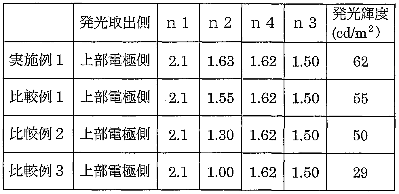
- the refractive index of the upper electrode (n 1: 2.1), the refractive index of the sealing medium (n 2: 1.63), the refractive index of the first color conversion medium (n 4: 1.62) and the refractive index of the sealing member (n3: 1.5) were set so as to satisfy the relational expression (2).
- peripheral portion was treated with a cationically curable adhesive TB3102 (manufactured by Three Pond Co., Ltd.), and then cured by light curing to obtain an organic EL display device of Example 1.
- a cationically curable adhesive TB3102 manufactured by Three Pond Co., Ltd.
- Example 1 as an evaluation of the first invention, an active matrix was placed between the upper electrode (anode, IZO) and the lower electrode (cathode, Al / Li) of the obtained organic EL display device. Light was emitted by applying a voltage of 12 V DC through a trix circuit.
- Comparative Example 1 a comparative example of the first invention was evaluated. Therefore, in Comparative Example 1, an organic EL display device was used in the same manner as in Example 1 except that silicon oil (refractive index: 1.55) was used instead of the PET resin used in Example 1. Create and review Valued. That is, the refractive index of the upper electrode (nl), the refractive index of the sealing medium (n2), the refractive index of the color conversion medium (n4), and the refractive index of the sealing member (n3) are expressed by the relational expression (2). Was not satisfied.
- the emission luminance of the obtained organic EL display device was measured using the color difference meter CS 1000 in the same manner as in Example 1, and a value of 55 cd / m 2 was obtained as shown in Table 1. .
- Comparative Example 1 it was confirmed that the emission luminance was reduced by about 11% while using the same organic EL element as in Example 1.
- Comparative Example 2 a comparative example of the first invention was evaluated. Therefore, in Comparative Example 2, instead of the O—PET resin in Example 1, the fluorine hydrocarbon liquid filler was replaced.
- An organic EL display device was prepared and evaluated in the same manner as in Example 1, except that a filler (refractive index: 1.3, manufactured by Sumitomo SLIM Co., Ltd.) was used. That is, the configuration was such that the values of the respective refractive indexes did not satisfy the relational expression (2).
- a filler reffractive index: 1.3, manufactured by Sumitomo SLIM Co., Ltd.
- Comparative Example 3 a comparative example of the first invention was evaluated. Therefore, in Comparative Example 3, an organic EL display device was prepared in the same manner as in Example 1 except that dry nitrogen (refractive index: 1.0) was used instead of the PET resin of Example 1. And evaluated. That is, the values of the refractive indices are configured so as not to satisfy the relational expression (2).
- Example 2 the second invention was evaluated. Therefore, in the second embodiment, as shown in FIG. 3, the first transparent resin layer 34 is provided between the lower electrode 22 and the second color conversion mediums 30 and 32, and the EL is provided from the lower electrode side. An organic EL display device 70 that emits light was created and evaluated.
- ⁇ ⁇ (refractive index: 1.8) was used as the lower electrode (transparent electrode), and the O-PET resin (refractive index: 1.63) used in Example 1 was used as the first transparent resin layer.
- a second conversion medium (refractive index: 1.62) is composed of a fluorescent medium 30 and a color filter 32, and a glass substrate (refractive index: 1.50) is used as the support substrate 10. The value of the rate was configured so as to satisfy the relational expression (8).
- Comparative Example 4 a comparative example of the second invention was evaluated. Therefore, in Comparative Example 4, an OLED display was used in the same manner as in Example 2 except that a SiO x sputtering film (refractive index: 1.50) was used instead of the ⁇ _PET resin in Example 2. A device was created and evaluated. That is, the values of the respective refractive indexes were set so as not to satisfy the relational expression (8).
- a SiO x sputtering film reffractive index: 1.50
- Example 3 In Example 3, another aspect of the second invention was evaluated. Therefore, in Example 3, an organic EL display device was prepared and evaluated according to Example 2, except that no color conversion medium was provided. That is, the refractive index of the lower electrode ( ⁇ 5), the refractive index of the transparent resin layer ( ⁇ 7), and the refractive index of the supporting substrate ( ⁇ 8) satisfy relational expression (6). Configured.
- Comparative Example 5 a comparative example of the second invention was evaluated. Therefore, in Comparative Example 5, an organic EL display was prepared in the same manner as in Example 3, except that polytrifluoroethylene (refractive index: 1.43) was used instead of the PET resin as the transparent resin layer in Example 3. A device was created and evaluated. That is, the refractive index (n5) of the lower electrode, the refractive index (n7) of the polytrifluoroethylene, and the refractive index (n8) of the supporting substrate do not satisfy the relational expression (6).
- polytrifluoroethylene reffractive index: 1.43
- Example 4 In Example 4, the third invention was evaluated. Therefore, in the fourth embodiment, the fourth color conversion medium of the third embodiment is provided on the side of the support substrate opposite to the side on which the transparent resin layer is provided, and the refractive index of the fourth color conversion medium is changed.
- the organic EL display device was fabricated in the same manner as in Example 3, except that PMMA (polymethyl methacrylate resin) was used as the matrix material and the lower electrode (anode) was made of IZO. And evaluated.
- the refractive index of the lower electrode (n5), the refractive index of the transparent resin layer (n7), the refractive index of the supporting substrate (n8), and the refractive index of the fourth color conversion medium (n9) are related. It was configured to satisfy equation (10).
- Comparative Example 6 a comparative example of the third invention was evaluated. Therefore, in Comparative Example 6, an organic EL display device was prepared in the same manner as in Example 4 except that polytrifluoroethylene (refractive index: 1.43) was used instead of the transparent resin layer in Example 4. And evaluated. That is, the refractive index (n5) of the lower electrode, the refractive index (n7) of polytrifluoroethylene, and the refractive index ( ⁇ 8) of the supporting substrate do not satisfy the relational expression (10).
- Example 5 the first invention was evaluated. That is, an organic EL display device was manufactured under the same conditions as in Example 1 except that a sealing member without a fluorescent medium was used.
- the refractive index of the upper electrode (nl: 2.1), the refractive index of the sealing medium (n2: 0—PET resin 1.63), and the refractive index of the sealing member (n3: 1.5) was configured to satisfy relational expression (1).
- Comparative Example 7 a comparative example of the first invention was evaluated. Therefore, in Comparative Example 7, except that nitrogen gas (refractive index: 1.00) was used as a sealing medium instead of the PET resin used in Example 5, An organic EL display was created and evaluated. That is, the refractive index (nl) of the upper electrode, the refractive index (n2) of the sealing medium, and the refractive index (n3) of the sealing member did not satisfy the relational expression (1).
- the relationship between the refractive index of the sealing member and the refractive index of the electrode or the like is considered without using silicon oil or the like as the sealing medium.
- the relationship between the refractive index of the color conversion medium or the transparent resin and the refractive index of the electrode or the like is taken into account.
- the relationship between the refractive index of the color conversion medium provided outside the support substrate and the refractive index of the electrode and the like is considered.
- the amount of EL emission that can be extracted to the outside can be increased by suppressing reflection at each interface.
Description


Claims
Priority Applications (3)
| Application Number | Priority Date | Filing Date | Title |
|---|---|---|---|
| EP01954372.7A EP1317165B1 (en) | 2000-08-23 | 2001-07-30 | Organic el display |
| US10/111,284 US6963168B2 (en) | 2000-08-23 | 2001-07-30 | Organic EL display device having certain relationships among constituent element refractive indices |
| US11/205,015 US7548020B2 (en) | 2000-08-23 | 2005-08-17 | Organic EL display device having certain relationships among constituent element refractive indices |
Applications Claiming Priority (2)
| Application Number | Priority Date | Filing Date | Title |
|---|---|---|---|
| JP2000-252231 | 2000-08-23 | ||
| JP2000252231 | 2000-08-23 |
Related Child Applications (1)
| Application Number | Title | Priority Date | Filing Date |
|---|---|---|---|
| US11/205,015 Continuation US7548020B2 (en) | 2000-08-23 | 2005-08-17 | Organic EL display device having certain relationships among constituent element refractive indices |
Publications (1)
| Publication Number | Publication Date |
|---|---|
| WO2002017689A1 true WO2002017689A1 (fr) | 2002-02-28 |
Family
ID=18741505
Family Applications (1)
| Application Number | Title | Priority Date | Filing Date |
|---|---|---|---|
| PCT/JP2001/006537 WO2002017689A1 (fr) | 2000-08-23 | 2001-07-30 | Afficheur electroluminescent organique |
Country Status (6)
| Country | Link |
|---|---|
| US (2) | US6963168B2 (ja) |
| EP (1) | EP1317165B1 (ja) |
| KR (2) | KR100748818B1 (ja) |
| CN (2) | CN101393967A (ja) |
| TW (1) | TWI244876B (ja) |
| WO (1) | WO2002017689A1 (ja) |
Cited By (25)
| Publication number | Priority date | Publication date | Assignee | Title |
|---|---|---|---|---|
| WO2004095892A1 (ja) * | 2003-04-24 | 2004-11-04 | Idemitsu Kosan Co., Ltd. | 有機エレクトロルミネッセンス素子及び表示装置 |
| JP2005209583A (ja) * | 2004-01-26 | 2005-08-04 | Semiconductor Energy Lab Co Ltd | 発光装置 |
| JP2005317302A (ja) * | 2004-04-28 | 2005-11-10 | Nippon Zeon Co Ltd | 有機el表示素子及びその製造方法 |
| JP2007066601A (ja) * | 2005-08-30 | 2007-03-15 | Victor Co Of Japan Ltd | 有機el表示装置 |
| JP2007519196A (ja) * | 2004-01-26 | 2007-07-12 | ケンブリッジ ディスプレイ テクノロジー リミテッド | 有機発光ダイオード |
| JP2007234391A (ja) * | 2006-03-01 | 2007-09-13 | Seiko Epson Corp | エレクトロルミネッセンス表示装置及び電子機器 |
| JP2007265870A (ja) * | 2006-03-29 | 2007-10-11 | Toppan Printing Co Ltd | 有機エレクトロルミネッセンス素子および表示装置 |
| JP2007265869A (ja) * | 2006-03-29 | 2007-10-11 | Toppan Printing Co Ltd | 有機エレクトロルミネッセンス素子および表示装置 |
| JP2007287486A (ja) * | 2006-04-17 | 2007-11-01 | Aitesu:Kk | 透明基板と電極の間に微細構造体を有する有機el素子 |
| JP2008016348A (ja) * | 2006-07-06 | 2008-01-24 | Toppan Printing Co Ltd | 有機エレクトロルミネッセンス素子および表示装置 |
| JP2008016347A (ja) * | 2006-07-06 | 2008-01-24 | Toppan Printing Co Ltd | 有機エレクトロルミネッセンス素子 |
| JP2008523546A (ja) * | 2004-12-06 | 2008-07-03 | コーニンクレッカ フィリップス エレクトロニクス エヌ ヴィ | 有機エレクトロルミネセント光源 |
| US7545095B2 (en) | 2003-01-21 | 2009-06-09 | Sanyo Electric Co., Ltd. | Electroluminescent display device |
| WO2009096498A1 (ja) * | 2008-01-31 | 2009-08-06 | Sumitomo Chemical Company, Limited | 透明導電膜付き透明板および有機エレクトロルミネッセンス素子 |
| WO2010032721A1 (ja) * | 2008-09-19 | 2010-03-25 | コニカミノルタホールディングス株式会社 | 有機エレクトロルミネッセンス素子 |
| WO2010035337A1 (ja) * | 2008-09-26 | 2010-04-01 | 富士電機ホールディングス株式会社 | 有機elデバイスおよびその製造方法 |
| JP2011096680A (ja) * | 2011-02-15 | 2011-05-12 | Semiconductor Energy Lab Co Ltd | 発光装置及び発光装置の作製方法 |
| JP2011108477A (ja) * | 2009-11-17 | 2011-06-02 | Fuji Electric Holdings Co Ltd | 有機elディスプレイ |
| WO2012108384A1 (ja) * | 2011-02-10 | 2012-08-16 | シャープ株式会社 | 蛍光体基板、およびこれを用いた表示装置、照明装置 |
| JP5020423B1 (ja) * | 2011-10-11 | 2012-09-05 | パイオニア株式会社 | 有機発光素子 |
| WO2017159503A1 (ja) * | 2016-03-15 | 2017-09-21 | シャープ株式会社 | 有機el表示装置 |
| JPWO2016151820A1 (ja) * | 2015-03-25 | 2017-11-30 | パイオニア株式会社 | 発光装置 |
| JP2019071305A (ja) * | 2019-02-18 | 2019-05-09 | パイオニア株式会社 | 発光装置 |
| JP2019172966A (ja) * | 2018-03-29 | 2019-10-10 | 大阪瓦斯株式会社 | 発光材料組成物 |
| JP2021015813A (ja) * | 2020-11-18 | 2021-02-12 | パイオニア株式会社 | 発光装置 |
Families Citing this family (72)
| Publication number | Priority date | Publication date | Assignee | Title |
|---|---|---|---|---|
| TW548860B (en) | 2001-06-20 | 2003-08-21 | Semiconductor Energy Lab | Light emitting device and method of manufacturing the same |
| US7211828B2 (en) | 2001-06-20 | 2007-05-01 | Semiconductor Energy Laboratory Co., Ltd. | Light emitting device and electronic apparatus |
| KR100563675B1 (ko) * | 2002-04-09 | 2006-03-28 | 캐논 가부시끼가이샤 | 유기 발광소자 및 유기 발광소자 패키지 |
| US7230271B2 (en) | 2002-06-11 | 2007-06-12 | Semiconductor Energy Laboratory Co., Ltd. | Light emitting device comprising film having hygroscopic property and transparency and manufacturing method thereof |
| JP2004207065A (ja) * | 2002-12-25 | 2004-07-22 | Fuji Electric Holdings Co Ltd | 色変換発光デバイスおよびその製造方法ならびに該デバイスを用いるディスプレイ |
| JP2004220874A (ja) * | 2003-01-14 | 2004-08-05 | Tohoku Pioneer Corp | 有機el素子、およびその製造方法 |
| JP2004227854A (ja) * | 2003-01-21 | 2004-08-12 | Sanyo Electric Co Ltd | エレクトロルミネッセンス表示装置 |
| US7109654B2 (en) * | 2003-03-14 | 2006-09-19 | Samsung Sdi Co., Ltd. | Electroluminescence device |
| CN100367531C (zh) * | 2003-09-15 | 2008-02-06 | 统宝光电股份有限公司 | 具有光效率提升结构的有机发光组件 |
| US20050062052A1 (en) * | 2003-09-23 | 2005-03-24 | Fu-Hsiang Yang | Panel of organic electroluminescent display |
| JP4547599B2 (ja) * | 2003-10-15 | 2010-09-22 | 奇美電子股▲ふん▼有限公司 | 画像表示装置 |
| JP4557755B2 (ja) * | 2004-03-11 | 2010-10-06 | キヤノン株式会社 | 基板、導電性基板および有機電界効果型トランジスタの各々の製造方法 |
| KR100666550B1 (ko) | 2004-04-07 | 2007-01-09 | 삼성에스디아이 주식회사 | 평판표시장치 및 그의 제조방법 |
| TWI231723B (en) * | 2004-04-16 | 2005-04-21 | Ind Tech Res Inst | Organic electroluminescence display device |
| US7202504B2 (en) | 2004-05-20 | 2007-04-10 | Semiconductor Energy Laboratory Co., Ltd. | Light-emitting element and display device |
| JP5124083B2 (ja) * | 2004-06-09 | 2013-01-23 | 三星ディスプレイ株式會社 | 有機電界発光表示装置及びその製造方法 |
| JP4618551B2 (ja) * | 2004-08-24 | 2011-01-26 | 富士電機ホールディングス株式会社 | 色変換フィルター基板および該色変換フィルター基板を具備した多色発光デバイス |
| US7342356B2 (en) * | 2004-09-23 | 2008-03-11 | 3M Innovative Properties Company | Organic electroluminescent device having protective structure with boron oxide layer and inorganic barrier layer |
| US20060063015A1 (en) * | 2004-09-23 | 2006-03-23 | 3M Innovative Properties Company | Protected polymeric film |
| KR100683693B1 (ko) * | 2004-11-10 | 2007-02-15 | 삼성에스디아이 주식회사 | 발광 장치 |
| JP4693593B2 (ja) * | 2004-11-16 | 2011-06-01 | 京セラ株式会社 | 発光装置 |
| KR100700013B1 (ko) * | 2004-11-26 | 2007-03-26 | 삼성에스디아이 주식회사 | 유기전계발광소자 및 그의 제조 방법 |
| US7960908B2 (en) * | 2005-07-15 | 2011-06-14 | Toshiba Matsushita Display Technology Co., Ltd. | Organic EL display |
| US20070193624A1 (en) * | 2006-02-23 | 2007-08-23 | Guardian Industries Corp. | Indium zinc oxide based front contact for photovoltaic device and method of making same |
| WO2008012079A1 (de) * | 2006-07-26 | 2008-01-31 | Leonhard Kurz Stiftung & Co. Kg | Organische solarzelle |
| JP4979299B2 (ja) * | 2006-08-03 | 2012-07-18 | 豊田合成株式会社 | 光学装置及びその製造方法 |
| KR100881455B1 (ko) * | 2006-08-14 | 2009-02-06 | 주식회사 잉크테크 | 유기전계발광소자 및 이의 제조방법 |
| US7969085B2 (en) * | 2006-08-18 | 2011-06-28 | Global Oled Technology Llc | Color-change material layer |
| US8012317B2 (en) * | 2006-11-02 | 2011-09-06 | Guardian Industries Corp. | Front electrode including transparent conductive coating on patterned glass substrate for use in photovoltaic device and method of making same |
| US8203073B2 (en) | 2006-11-02 | 2012-06-19 | Guardian Industries Corp. | Front electrode for use in photovoltaic device and method of making same |
| US20080178932A1 (en) * | 2006-11-02 | 2008-07-31 | Guardian Industries Corp. | Front electrode including transparent conductive coating on patterned glass substrate for use in photovoltaic device and method of making same |
| US8076571B2 (en) * | 2006-11-02 | 2011-12-13 | Guardian Industries Corp. | Front electrode for use in photovoltaic device and method of making same |
| US20080105299A1 (en) * | 2006-11-02 | 2008-05-08 | Guardian Industries Corp. | Front electrode with thin metal film layer and high work-function buffer layer for use in photovoltaic device and method of making same |
| US7964788B2 (en) * | 2006-11-02 | 2011-06-21 | Guardian Industries Corp. | Front electrode for use in photovoltaic device and method of making same |
| US20080105298A1 (en) * | 2006-11-02 | 2008-05-08 | Guardian Industries Corp. | Front electrode for use in photovoltaic device and method of making same |
| US20100051920A1 (en) * | 2006-12-20 | 2010-03-04 | Dow Corning Corporation | Composite Article Including a Cation-Sensitive Layer |
| US8334452B2 (en) * | 2007-01-08 | 2012-12-18 | Guardian Industries Corp. | Zinc oxide based front electrode doped with yttrium for use in photovoltaic device or the like |
| US7767253B2 (en) * | 2007-03-09 | 2010-08-03 | Guardian Industries Corp. | Method of making a photovoltaic device with antireflective coating |
| US20080223430A1 (en) * | 2007-03-14 | 2008-09-18 | Guardian Industries Corp. | Buffer layer for front electrode structure in photovoltaic device or the like |
| US8237047B2 (en) * | 2007-05-01 | 2012-08-07 | Guardian Industries Corp. | Method of making a photovoltaic device or front substrate for use in same with scratch-resistant coating and resulting product |
| US20080295884A1 (en) * | 2007-05-29 | 2008-12-04 | Sharma Pramod K | Method of making a photovoltaic device or front substrate with barrier layer for use in same and resulting product |
| US20080308145A1 (en) * | 2007-06-12 | 2008-12-18 | Guardian Industries Corp | Front electrode including transparent conductive coating on etched glass substrate for use in photovoltaic device and method of making same |
| JP2008311059A (ja) * | 2007-06-14 | 2008-12-25 | Rohm Co Ltd | 有機エレクトロルミネセンス素子及びその製造方法 |
| US20080308146A1 (en) * | 2007-06-14 | 2008-12-18 | Guardian Industries Corp. | Front electrode including pyrolytic transparent conductive coating on textured glass substrate for use in photovoltaic device and method of making same |
| JP5208591B2 (ja) | 2007-06-28 | 2013-06-12 | 株式会社半導体エネルギー研究所 | 発光装置、及び照明装置 |
| CN101627662B (zh) * | 2007-09-06 | 2012-02-01 | 索尼株式会社 | 光提取装置、光提取装置制造方法以及显示设备 |
| EP2040316B1 (de) * | 2007-09-20 | 2014-08-06 | OSRAM Opto Semiconductors GmbH | Optoelektronisches Bauelement und Verfahren zur Herstellung eines optoelektronischen Bauelements |
| DE102007052181A1 (de) * | 2007-09-20 | 2009-04-02 | Osram Opto Semiconductors Gmbh | Optoelektronisches Bauelement und Verfahren zur Herstellung eines optoelektronischen Bauelements |
| KR101383490B1 (ko) * | 2007-09-21 | 2014-04-08 | 엘지디스플레이 주식회사 | 전계발광소자 |
| US7888594B2 (en) * | 2007-11-20 | 2011-02-15 | Guardian Industries Corp. | Photovoltaic device including front electrode having titanium oxide inclusive layer with high refractive index |
| US8114472B2 (en) * | 2008-01-08 | 2012-02-14 | Guardian Industries Corp. | Method of making a temperable antiglare coating, and resulting products containing the same |
| US20090194155A1 (en) * | 2008-02-01 | 2009-08-06 | Guardian Industries Corp. | Front electrode having etched surface for use in photovoltaic device and method of making same |
| US20090194157A1 (en) * | 2008-02-01 | 2009-08-06 | Guardian Industries Corp. | Front electrode having etched surface for use in photovoltaic device and method of making same |
| JP5515237B2 (ja) * | 2008-05-14 | 2014-06-11 | セイコーエプソン株式会社 | 発光装置及び電子機器 |
| KR100953658B1 (ko) * | 2008-06-05 | 2010-04-20 | 삼성모바일디스플레이주식회사 | 유기전계발광 표시장치 |
| TWI405836B (zh) * | 2008-09-26 | 2013-08-21 | Lite On Electronics Guangzhou | 螢光材料 |
| US8022291B2 (en) * | 2008-10-15 | 2011-09-20 | Guardian Industries Corp. | Method of making front electrode of photovoltaic device having etched surface and corresponding photovoltaic device |
| KR101006400B1 (ko) * | 2009-04-17 | 2011-01-10 | (주)이지스테크 | 온도 유지부를 갖는 조명 장치 |
| US20120112618A1 (en) * | 2009-07-29 | 2012-05-10 | Sharp Kabushiki Kaisha | Organic electroluminescence illuminating device and method for manufacturing the same |
| JPWO2011040238A1 (ja) * | 2009-09-30 | 2013-02-28 | 凸版印刷株式会社 | 有機エレクトロルミネッセンス素子及びそれを用いた表示装置並びに有機エレクトロルミネッセンス素子の製造方法 |
| KR101039930B1 (ko) * | 2009-10-23 | 2011-06-09 | 엘지이노텍 주식회사 | 발광소자 패키지 및 그 제조방법 |
| TWI457883B (zh) * | 2011-03-11 | 2014-10-21 | E Ink Holdings Inc | 彩色顯示裝置 |
| DE102011084437A1 (de) * | 2011-10-13 | 2013-04-18 | Osram Opto Semiconductors Gmbh | Lichtemittierendes Bauelement und Verfahren zum Herstellen eines lichtemittierenden Bauelements |
| DE102011084889A1 (de) * | 2011-10-20 | 2013-04-25 | Osram Opto Semiconductors Gmbh | Lichtemittierendes Bauelement und Verfahren zum Herstellen eines lichtemittierenden Bauelements |
| TW201414030A (zh) * | 2012-09-17 | 2014-04-01 | Wintek Corp | 有機發光二極體 |
| CN103715358A (zh) * | 2012-10-09 | 2014-04-09 | 东莞万士达液晶显示器有限公司 | 有机发光二极管 |
| JP6223070B2 (ja) * | 2013-08-29 | 2017-11-01 | 株式会社ジャパンディスプレイ | 有機el表示装置及び有機el表示装置の製造方法 |
| DE102013110024B9 (de) | 2013-09-12 | 2023-11-09 | Pictiva Displays International Limited | Strahlungsemittierendes Bauelement mit organischem Schichtenstapel |
| KR102343656B1 (ko) * | 2015-01-15 | 2021-12-27 | 삼성디스플레이 주식회사 | 유기 발광 표시 장치 |
| CN209265407U (zh) * | 2016-07-01 | 2019-08-16 | Lg伊诺特有限公司 | 指纹传感器盖、指纹感测装置及包括其的触摸装置 |
| CN109886163B (zh) * | 2019-01-30 | 2021-08-06 | 武汉华星光电半导体显示技术有限公司 | 具有指纹辨识功能的显示装置及其制造方法 |
| WO2020208774A1 (ja) * | 2019-04-11 | 2020-10-15 | シャープ株式会社 | 発光素子および表示装置 |
Citations (4)
| Publication number | Priority date | Publication date | Assignee | Title |
|---|---|---|---|---|
| JPH07272857A (ja) * | 1994-03-31 | 1995-10-20 | Nippondenso Co Ltd | エレクトロルミネッセンス素子およびその製造方法 |
| JPH10162958A (ja) * | 1996-11-28 | 1998-06-19 | Casio Comput Co Ltd | El素子 |
| JPH10289784A (ja) * | 1997-04-14 | 1998-10-27 | Mitsubishi Chem Corp | 有機電界発光素子 |
| JPH11185955A (ja) * | 1997-12-22 | 1999-07-09 | Tdk Corp | 有機elカラーディスプレイ |
Family Cites Families (21)
| Publication number | Priority date | Publication date | Assignee | Title |
|---|---|---|---|---|
| US4794302A (en) | 1986-01-08 | 1988-12-27 | Kabushiki Kaisha Komatsu Seisakusho | Thin film el device and method of manufacturing the same |
| JPH07211458A (ja) | 1994-01-17 | 1995-08-11 | Fuji Electric Co Ltd | 薄膜発光素子 |
| US5725044A (en) | 1994-08-30 | 1998-03-10 | Hirokawa; Koji | Casting method using a forming die |
| JPH08142256A (ja) * | 1994-11-25 | 1996-06-04 | Kureha Chem Ind Co Ltd | 防湿複合蒸着フィルム |
| US5814516A (en) * | 1995-10-13 | 1998-09-29 | Lockheed Martin Energy Systems, Inc. | Surface enhanced Raman gene probe and methods thereof |
| TW364275B (en) * | 1996-03-12 | 1999-07-11 | Idemitsu Kosan Co | Organic electroluminescent element and organic electroluminescent display device |
| US5814416A (en) * | 1996-04-10 | 1998-09-29 | Lucent Technologies, Inc. | Wavelength compensation for resonant cavity electroluminescent devices |
| US5693956A (en) * | 1996-07-29 | 1997-12-02 | Motorola | Inverted oleds on hard plastic substrate |
| JP3691192B2 (ja) | 1997-01-31 | 2005-08-31 | 三洋電機株式会社 | 有機エレクトロルミネッセンス素子 |
| US5869929A (en) | 1997-02-04 | 1999-02-09 | Idemitsu Kosan Co., Ltd. | Multicolor luminescent device |
| JPH1131590A (ja) * | 1997-07-09 | 1999-02-02 | Tdk Corp | 有機el素子 |
| KR100382539B1 (ko) * | 1997-09-11 | 2004-05-17 | 주식회사 하이닉스반도체 | 반도체소자의 전극 보호막 형성방법 |
| JPH11195487A (ja) * | 1997-12-27 | 1999-07-21 | Tdk Corp | 有機el素子 |
| JP2000058270A (ja) * | 1998-08-04 | 2000-02-25 | Sony Corp | 光学素子および有機elディスプレイ |
| JP2000206894A (ja) * | 1998-11-10 | 2000-07-28 | Toshiba Corp | 平面表示装置 |
| JP4136185B2 (ja) * | 1999-05-12 | 2008-08-20 | パイオニア株式会社 | 有機エレクトロルミネッセンス多色ディスプレイ及びその製造方法 |
| TW527735B (en) * | 1999-06-04 | 2003-04-11 | Semiconductor Energy Lab | Electro-optical device |
| JP3463866B2 (ja) * | 1999-09-24 | 2003-11-05 | 富士電機株式会社 | 蛍光色変換膜、それを用いた蛍光色変換フィルターおよび該蛍光色変換フィルターを具備した有機発光素子 |
| US6573652B1 (en) * | 1999-10-25 | 2003-06-03 | Battelle Memorial Institute | Encapsulated display devices |
| US6633121B2 (en) * | 2000-01-31 | 2003-10-14 | Idemitsu Kosan Co., Ltd. | Organic electroluminescence display device and method of manufacturing same |
| TW484238B (en) * | 2000-03-27 | 2002-04-21 | Semiconductor Energy Lab | Light emitting device and a method of manufacturing the same |
-
2001
- 2001-07-30 CN CNA2006101688211A patent/CN101393967A/zh active Pending
- 2001-07-30 CN CN01802513A patent/CN1389085A/zh active Pending
- 2001-07-30 KR KR1020027005219A patent/KR100748818B1/ko active IP Right Grant
- 2001-07-30 EP EP01954372.7A patent/EP1317165B1/en not_active Expired - Lifetime
- 2001-07-30 KR KR1020077009105A patent/KR100773674B1/ko active IP Right Grant
- 2001-07-30 US US10/111,284 patent/US6963168B2/en not_active Expired - Lifetime
- 2001-07-30 WO PCT/JP2001/006537 patent/WO2002017689A1/ja active Application Filing
- 2001-08-03 TW TW090119037A patent/TWI244876B/zh not_active IP Right Cessation
-
2005
- 2005-08-17 US US11/205,015 patent/US7548020B2/en not_active Expired - Fee Related
Patent Citations (4)
| Publication number | Priority date | Publication date | Assignee | Title |
|---|---|---|---|---|
| JPH07272857A (ja) * | 1994-03-31 | 1995-10-20 | Nippondenso Co Ltd | エレクトロルミネッセンス素子およびその製造方法 |
| JPH10162958A (ja) * | 1996-11-28 | 1998-06-19 | Casio Comput Co Ltd | El素子 |
| JPH10289784A (ja) * | 1997-04-14 | 1998-10-27 | Mitsubishi Chem Corp | 有機電界発光素子 |
| JPH11185955A (ja) * | 1997-12-22 | 1999-07-09 | Tdk Corp | 有機elカラーディスプレイ |
Cited By (41)
| Publication number | Priority date | Publication date | Assignee | Title |
|---|---|---|---|---|
| US8557333B2 (en) | 2003-01-21 | 2013-10-15 | Sanyo Electric Co., Ltd. | Electroluminescent display device |
| US7545095B2 (en) | 2003-01-21 | 2009-06-09 | Sanyo Electric Co., Ltd. | Electroluminescent display device |
| JPWO2004095892A1 (ja) * | 2003-04-24 | 2006-07-13 | 出光興産株式会社 | 有機エレクトロルミネッセンス素子及び表示装置 |
| US7358661B2 (en) | 2003-04-24 | 2008-04-15 | Idemitsu Kosan Co., Ltd. | Organic electroluminescent device and display |
| WO2004095892A1 (ja) * | 2003-04-24 | 2004-11-04 | Idemitsu Kosan Co., Ltd. | 有機エレクトロルミネッセンス素子及び表示装置 |
| JP2005209583A (ja) * | 2004-01-26 | 2005-08-04 | Semiconductor Energy Lab Co Ltd | 発光装置 |
| JP2007519196A (ja) * | 2004-01-26 | 2007-07-12 | ケンブリッジ ディスプレイ テクノロジー リミテッド | 有機発光ダイオード |
| JP2005317302A (ja) * | 2004-04-28 | 2005-11-10 | Nippon Zeon Co Ltd | 有機el表示素子及びその製造方法 |
| JP4736348B2 (ja) * | 2004-04-28 | 2011-07-27 | 日本ゼオン株式会社 | 有機el素子の製造方法 |
| JP4769254B2 (ja) * | 2004-12-06 | 2011-09-07 | コーニンクレッカ フィリップス エレクトロニクス エヌ ヴィ | 有機エレクトロルミネセント光源 |
| JP2008523546A (ja) * | 2004-12-06 | 2008-07-03 | コーニンクレッカ フィリップス エレクトロニクス エヌ ヴィ | 有機エレクトロルミネセント光源 |
| JP2007066601A (ja) * | 2005-08-30 | 2007-03-15 | Victor Co Of Japan Ltd | 有機el表示装置 |
| JP2007234391A (ja) * | 2006-03-01 | 2007-09-13 | Seiko Epson Corp | エレクトロルミネッセンス表示装置及び電子機器 |
| JP2007265869A (ja) * | 2006-03-29 | 2007-10-11 | Toppan Printing Co Ltd | 有機エレクトロルミネッセンス素子および表示装置 |
| JP2007265870A (ja) * | 2006-03-29 | 2007-10-11 | Toppan Printing Co Ltd | 有機エレクトロルミネッセンス素子および表示装置 |
| JP2007287486A (ja) * | 2006-04-17 | 2007-11-01 | Aitesu:Kk | 透明基板と電極の間に微細構造体を有する有機el素子 |
| JP2008016348A (ja) * | 2006-07-06 | 2008-01-24 | Toppan Printing Co Ltd | 有機エレクトロルミネッセンス素子および表示装置 |
| JP4739134B2 (ja) * | 2006-07-06 | 2011-08-03 | 凸版印刷株式会社 | 有機エレクトロルミネッセンス素子および表示装置 |
| JP2008016347A (ja) * | 2006-07-06 | 2008-01-24 | Toppan Printing Co Ltd | 有機エレクトロルミネッセンス素子 |
| JP4739133B2 (ja) * | 2006-07-06 | 2011-08-03 | 凸版印刷株式会社 | 有機エレクトロルミネッセンス素子 |
| US8471457B2 (en) | 2008-01-31 | 2013-06-25 | Sumitomo Chemical Company, Limited | Transparent plate with transparent conductive film and organic electroluminescence element |
| WO2009096498A1 (ja) * | 2008-01-31 | 2009-08-06 | Sumitomo Chemical Company, Limited | 透明導電膜付き透明板および有機エレクトロルミネッセンス素子 |
| JPWO2010032721A1 (ja) * | 2008-09-19 | 2012-02-09 | コニカミノルタホールディングス株式会社 | 有機エレクトロルミネッセンス素子 |
| WO2010032721A1 (ja) * | 2008-09-19 | 2010-03-25 | コニカミノルタホールディングス株式会社 | 有機エレクトロルミネッセンス素子 |
| US8304984B2 (en) | 2008-09-19 | 2012-11-06 | Konica Minolta Holdings, Inc. | Organic electroluminescent element |
| JP5378354B2 (ja) * | 2008-09-26 | 2013-12-25 | シャープ株式会社 | 有機elデバイスおよびその製造方法 |
| TWI486092B (zh) * | 2008-09-26 | 2015-05-21 | Sharp Kk | 有機電激發光裝置及其製造方法 |
| WO2010035337A1 (ja) * | 2008-09-26 | 2010-04-01 | 富士電機ホールディングス株式会社 | 有機elデバイスおよびその製造方法 |
| US8487299B2 (en) | 2008-09-26 | 2013-07-16 | Sharp Kabushiki Kaisha | Organic EL device and method of manufacturing same |
| JP2011108477A (ja) * | 2009-11-17 | 2011-06-02 | Fuji Electric Holdings Co Ltd | 有機elディスプレイ |
| WO2012108384A1 (ja) * | 2011-02-10 | 2012-08-16 | シャープ株式会社 | 蛍光体基板、およびこれを用いた表示装置、照明装置 |
| JP2011096680A (ja) * | 2011-02-15 | 2011-05-12 | Semiconductor Energy Lab Co Ltd | 発光装置及び発光装置の作製方法 |
| JP5020423B1 (ja) * | 2011-10-11 | 2012-09-05 | パイオニア株式会社 | 有機発光素子 |
| WO2013054392A1 (ja) * | 2011-10-11 | 2013-04-18 | パイオニア株式会社 | 有機発光素子 |
| JPWO2016151820A1 (ja) * | 2015-03-25 | 2017-11-30 | パイオニア株式会社 | 発光装置 |
| WO2017159503A1 (ja) * | 2016-03-15 | 2017-09-21 | シャープ株式会社 | 有機el表示装置 |
| US20190081110A1 (en) * | 2016-03-15 | 2019-03-14 | Sharp Kabushiki Kaisha | Organic el display device |
| US10468467B2 (en) | 2016-03-15 | 2019-11-05 | Sharp Kabushiki Kaisha | Organic electroluminescence display device |
| JP2019172966A (ja) * | 2018-03-29 | 2019-10-10 | 大阪瓦斯株式会社 | 発光材料組成物 |
| JP2019071305A (ja) * | 2019-02-18 | 2019-05-09 | パイオニア株式会社 | 発光装置 |
| JP2021015813A (ja) * | 2020-11-18 | 2021-02-12 | パイオニア株式会社 | 発光装置 |
Also Published As
| Publication number | Publication date |
|---|---|
| CN101393967A (zh) | 2009-03-25 |
| CN1389085A (zh) | 2003-01-01 |
| KR100748818B1 (ko) | 2007-08-13 |
| US7548020B2 (en) | 2009-06-16 |
| EP1317165A1 (en) | 2003-06-04 |
| US6963168B2 (en) | 2005-11-08 |
| KR20020044565A (ko) | 2002-06-15 |
| KR100773674B1 (ko) | 2007-11-05 |
| EP1317165B1 (en) | 2013-12-04 |
| KR20070049248A (ko) | 2007-05-10 |
| US20050275346A1 (en) | 2005-12-15 |
| US20030071567A1 (en) | 2003-04-17 |
| TWI244876B (en) | 2005-12-01 |
Similar Documents
| Publication | Publication Date | Title |
|---|---|---|
| WO2002017689A1 (fr) | Afficheur electroluminescent organique | |
| TWI272866B (en) | Organic electroluminescent display and method for manufacturing same | |
| JP3962572B2 (ja) | 有機エレクトロルミネッセンス発光装置 | |
| JP4603754B2 (ja) | 有機エレクトロルミネッセンス表示装置およびその製造方法 | |
| US7583021B2 (en) | Composite emitting device | |
| KR100529450B1 (ko) | 유기 전자 발광 표시 장치 | |
| JP5236732B2 (ja) | 色変換膜及び該色変換膜を含む多色発光有機elデバイス | |
| US20050146266A1 (en) | Organic el display and its production method | |
| US20080001528A1 (en) | Color conversion substrate and color display | |
| US20080036367A1 (en) | Organic El Display Device | |
| JPWO2006028089A1 (ja) | 発光デバイスおよびその製造方法 | |
| JPH1126156A (ja) | 有機el多色発光表示装置 | |
| JP2007207655A (ja) | 有機elディスプレイ | |
| JPWO2005046291A1 (ja) | 発光表示装置用バリア膜及びその製造方法 | |
| JP5450738B2 (ja) | 色変換膜及び該色変換膜を含む有機elデバイス | |
| JP2009288476A (ja) | 色変換基板の製造方法、色変換フィルタ基板の製造方法及び有機電界発光素子の製造方法 | |
| JP2003297547A (ja) | 有機el表示装置 | |
| WO2009099009A1 (ja) | 有機elディスプレイおよびその製造方法 | |
| JP2006269227A (ja) | 多色発光デバイス及びその製造方法 |
Legal Events
| Date | Code | Title | Description |
|---|---|---|---|
| AK | Designated states |
Kind code of ref document: A1 Designated state(s): CN JP KR US |
|
| AL | Designated countries for regional patents |
Kind code of ref document: A1 Designated state(s): AT BE CH CY DE DK ES FI FR GB GR IE IT LU MC NL PT SE TR |
|
| ENP | Entry into the national phase |
Ref country code: JP Ref document number: 2002 521419 Kind code of ref document: A Format of ref document f/p: F |
|
| WWE | Wipo information: entry into national phase |
Ref document number: 2001954372 Country of ref document: EP |
|
| WWE | Wipo information: entry into national phase |
Ref document number: 10111284 Country of ref document: US |
|
| WWE | Wipo information: entry into national phase |
Ref document number: 1020027005219 Country of ref document: KR Ref document number: 018025137 Country of ref document: CN |
|
| 121 | Ep: the epo has been informed by wipo that ep was designated in this application | ||
| WWP | Wipo information: published in national office |
Ref document number: 1020027005219 Country of ref document: KR |
|
| WWP | Wipo information: published in national office |
Ref document number: 2001954372 Country of ref document: EP |