WO1995006336A1 - Electrode multicouche a couches minces utilisee pour le couplage de champs electromagnetiques a hautes frequences - Google Patents
Electrode multicouche a couches minces utilisee pour le couplage de champs electromagnetiques a hautes frequences Download PDFInfo
- Publication number
- WO1995006336A1 WO1995006336A1 PCT/JP1994/000357 JP9400357W WO9506336A1 WO 1995006336 A1 WO1995006336 A1 WO 1995006336A1 JP 9400357 W JP9400357 W JP 9400357W WO 9506336 A1 WO9506336 A1 WO 9506336A1
- Authority
- WO
- WIPO (PCT)
- Prior art keywords
- thin film
- frequency
- transmission line
- conductor
- dielectric
- Prior art date
Links
- 239000010409 thin film Substances 0.000 title claims abstract description 321
- 230000005672 electromagnetic field Effects 0.000 title claims abstract description 79
- 230000008878 coupling Effects 0.000 title description 29
- 238000010168 coupling process Methods 0.000 title description 29
- 238000005859 coupling reaction Methods 0.000 title description 29
- 239000004020 conductor Substances 0.000 claims abstract description 267
- 230000005540 biological transmission Effects 0.000 claims abstract description 250
- 239000003989 dielectric material Substances 0.000 claims abstract description 46
- 239000010408 film Substances 0.000 claims description 56
- 239000000758 substrate Substances 0.000 claims description 37
- 239000000463 material Substances 0.000 claims description 23
- 230000001902 propagating effect Effects 0.000 claims description 22
- 238000010030 laminating Methods 0.000 claims description 7
- 239000000411 inducer Substances 0.000 claims description 3
- 230000001965 increasing effect Effects 0.000 abstract description 12
- 230000000644 propagated effect Effects 0.000 abstract description 2
- 210000003491 skin Anatomy 0.000 description 24
- 238000009826 distribution Methods 0.000 description 22
- 238000004088 simulation Methods 0.000 description 17
- 238000010586 diagram Methods 0.000 description 14
- 239000003990 capacitor Substances 0.000 description 11
- 208000032370 Secondary transmission Diseases 0.000 description 6
- 230000002093 peripheral effect Effects 0.000 description 5
- 238000006073 displacement reaction Methods 0.000 description 4
- 230000002500 effect on skin Effects 0.000 description 4
- 230000004048 modification Effects 0.000 description 4
- 238000012986 modification Methods 0.000 description 4
- YMWLPMGFZYFLRP-UHFFFAOYSA-N 2-(4,5-dimethyl-1,3-diselenol-2-ylidene)-4,5-dimethyl-1,3-diselenole Chemical compound [Se]1C(C)=C(C)[Se]C1=C1[Se]C(C)=C(C)[Se]1 YMWLPMGFZYFLRP-UHFFFAOYSA-N 0.000 description 3
- LZJCVNLYDXCIBG-UHFFFAOYSA-N 2-(5,6-dihydro-[1,3]dithiolo[4,5-b][1,4]dithiin-2-ylidene)-5,6-dihydro-[1,3]dithiolo[4,5-b][1,4]dithiine Chemical compound S1C(SCCS2)=C2SC1=C(S1)SC2=C1SCCS2 LZJCVNLYDXCIBG-UHFFFAOYSA-N 0.000 description 3
- 229910045601 alloy Inorganic materials 0.000 description 3
- 239000000956 alloy Substances 0.000 description 3
- 230000005684 electric field Effects 0.000 description 3
- 230000005284 excitation Effects 0.000 description 3
- 239000010931 gold Substances 0.000 description 3
- 238000000034 method Methods 0.000 description 3
- 238000005457 optimization Methods 0.000 description 3
- 230000009467 reduction Effects 0.000 description 3
- 230000015572 biosynthetic process Effects 0.000 description 2
- 229910052802 copper Inorganic materials 0.000 description 2
- 230000000694 effects Effects 0.000 description 2
- 230000008030 elimination Effects 0.000 description 2
- 238000003379 elimination reaction Methods 0.000 description 2
- 229910052737 gold Inorganic materials 0.000 description 2
- 230000005404 monopole Effects 0.000 description 2
- 230000035699 permeability Effects 0.000 description 2
- 239000000843 powder Substances 0.000 description 2
- 230000008569 process Effects 0.000 description 2
- 239000000047 product Substances 0.000 description 2
- 230000001681 protective effect Effects 0.000 description 2
- 229910052709 silver Inorganic materials 0.000 description 2
- 239000002887 superconductor Substances 0.000 description 2
- 206010021143 Hypoxia Diseases 0.000 description 1
- PNEYBMLMFCGWSK-UHFFFAOYSA-N aluminium oxide Inorganic materials [O-2].[O-2].[O-2].[Al+3].[Al+3] PNEYBMLMFCGWSK-UHFFFAOYSA-N 0.000 description 1
- 230000001174 ascending effect Effects 0.000 description 1
- QVGXLLKOCUKJST-UHFFFAOYSA-N atomic oxygen Chemical compound [O] QVGXLLKOCUKJST-UHFFFAOYSA-N 0.000 description 1
- 239000005667 attractant Substances 0.000 description 1
- 239000011230 binding agent Substances 0.000 description 1
- 238000001354 calcination Methods 0.000 description 1
- 239000000969 carrier Substances 0.000 description 1
- 239000000919 ceramic Substances 0.000 description 1
- 238000006243 chemical reaction Methods 0.000 description 1
- 230000031902 chemoattractant activity Effects 0.000 description 1
- 238000005094 computer simulation Methods 0.000 description 1
- 235000009508 confectionery Nutrition 0.000 description 1
- 238000007796 conventional method Methods 0.000 description 1
- 239000013078 crystal Substances 0.000 description 1
- 230000005611 electricity Effects 0.000 description 1
- 238000005516 engineering process Methods 0.000 description 1
- 210000002615 epidermis Anatomy 0.000 description 1
- 239000007789 gas Substances 0.000 description 1
- PCHJSUWPFVWCPO-UHFFFAOYSA-N gold Chemical compound [Au] PCHJSUWPFVWCPO-UHFFFAOYSA-N 0.000 description 1
- 230000012447 hatching Effects 0.000 description 1
- 230000001939 inductive effect Effects 0.000 description 1
- 229910000765 intermetallic Inorganic materials 0.000 description 1
- 238000003475 lamination Methods 0.000 description 1
- 229910052745 lead Inorganic materials 0.000 description 1
- 239000007788 liquid Substances 0.000 description 1
- 238000000465 moulding Methods 0.000 description 1
- 229910052758 niobium Inorganic materials 0.000 description 1
- 239000001301 oxygen Substances 0.000 description 1
- 229910052760 oxygen Inorganic materials 0.000 description 1
- 230000035515 penetration Effects 0.000 description 1
- 239000012466 permeate Substances 0.000 description 1
- 239000010453 quartz Substances 0.000 description 1
- 229910052594 sapphire Inorganic materials 0.000 description 1
- 239000010980 sapphire Substances 0.000 description 1
- VYPSYNLAJGMNEJ-UHFFFAOYSA-N silicon dioxide Inorganic materials O=[Si]=O VYPSYNLAJGMNEJ-UHFFFAOYSA-N 0.000 description 1
- 238000005245 sintering Methods 0.000 description 1
- 239000007787 solid Substances 0.000 description 1
- 229910052718 tin Inorganic materials 0.000 description 1
Classifications
-
- H—ELECTRICITY
- H01—ELECTRIC ELEMENTS
- H01P—WAVEGUIDES; RESONATORS, LINES, OR OTHER DEVICES OF THE WAVEGUIDE TYPE
- H01P7/00—Resonators of the waveguide type
- H01P7/08—Strip line resonators
- H01P7/082—Microstripline resonators
-
- H—ELECTRICITY
- H01—ELECTRIC ELEMENTS
- H01P—WAVEGUIDES; RESONATORS, LINES, OR OTHER DEVICES OF THE WAVEGUIDE TYPE
- H01P1/00—Auxiliary devices
- H01P1/20—Frequency-selective devices, e.g. filters
-
- H—ELECTRICITY
- H01—ELECTRIC ELEMENTS
- H01P—WAVEGUIDES; RESONATORS, LINES, OR OTHER DEVICES OF THE WAVEGUIDE TYPE
- H01P1/00—Auxiliary devices
- H01P1/20—Frequency-selective devices, e.g. filters
- H01P1/201—Filters for transverse electromagnetic waves
- H01P1/203—Strip line filters
-
- H—ELECTRICITY
- H01—ELECTRIC ELEMENTS
- H01P—WAVEGUIDES; RESONATORS, LINES, OR OTHER DEVICES OF THE WAVEGUIDE TYPE
- H01P3/00—Waveguides; Transmission lines of the waveguide type
- H01P3/02—Waveguides; Transmission lines of the waveguide type with two longitudinal conductors
- H01P3/06—Coaxial lines
-
- H—ELECTRICITY
- H01—ELECTRIC ELEMENTS
- H01P—WAVEGUIDES; RESONATORS, LINES, OR OTHER DEVICES OF THE WAVEGUIDE TYPE
- H01P3/00—Waveguides; Transmission lines of the waveguide type
- H01P3/02—Waveguides; Transmission lines of the waveguide type with two longitudinal conductors
- H01P3/08—Microstrips; Strip lines
- H01P3/088—Stacked transmission lines
-
- H—ELECTRICITY
- H01—ELECTRIC ELEMENTS
- H01P—WAVEGUIDES; RESONATORS, LINES, OR OTHER DEVICES OF THE WAVEGUIDE TYPE
- H01P3/00—Waveguides; Transmission lines of the waveguide type
- H01P3/18—Waveguides; Transmission lines of the waveguide type built-up from several layers to increase operating surface, i.e. alternately conductive and dielectric layers
-
- H—ELECTRICITY
- H10—SEMICONDUCTOR DEVICES; ELECTRIC SOLID-STATE DEVICES NOT OTHERWISE PROVIDED FOR
- H10N—ELECTRIC SOLID-STATE DEVICES NOT OTHERWISE PROVIDED FOR
- H10N60/00—Superconducting devices
- H10N60/80—Constructional details
- H10N60/85—Superconducting active materials
- H10N60/855—Ceramic superconductors
- H10N60/857—Ceramic superconductors comprising copper oxide
- H10N60/858—Ceramic superconductors comprising copper oxide having multilayered structures, e.g. superlattices
Definitions
- the present invention uses a high-frequency electromagnetic field-coupled thin-film laminated electrode used in the high-frequency band of microwave, quasi-millimeter wave, or mill-wave, a high-frequency transmission line using the thin-film laminated electrode, and the thin-film laminated transmission line.
- the present invention relates to a high-frequency resonator, a high-frequency filter equipped with the high-frequency resonator, and a high-frequency device equipped with the thin-film laminated electrode.
- the energy loss of high-frequency devices can be broadly classified into the conductor loss due to the skin effect and the dielectric loss due to the dielectric material.
- dielectric materials with high dielectric constant but low loss characteristics have been developed and put into practical use. Therefore, conductor loss is more dominant in the no-load Q of the circuit than dielectric loss. be.
- high-frequency current is concentrated on the surface of the conductor due to the skin effect, so the closer to the surface of the conductor, the more the surface resistance.
- a conventional resonator that can effectively reduce conductor loss and obtain a high no-load Q has been patented in Japan. Published 1992 (1992) Proposed in Gazette No. 4 3 7 0 3.
- a resonant circuit is formed by a symmetric strip line in which strip conductors are arranged between a pair of ground conductors that are opposed to each other with a dielectric material in between.
- a plurality of the above-mentioned strip conductors are arranged in a laminated manner between the above-mentioned pair of grounding conductors in parallel with the above-mentioned grounding conductors at a predetermined distance from each other via the above-mentioned dielectric material. It is characterized by that.
- each of the strip conductors is formed with a thickness of 3 times or more than the skin depth in order to effectively suppress the conductor loss. That is, in the strip conductor, the skin portion through which the high-frequency current in the microwave band flows is increased, and the effective cross-sectional area in the strip conductor is increased.
- One end side of the pair of strip conductors conducts to each other through through holes, while the other end side also conducts to each other through through holes.
- An object of the present invention is to solve the above problems, to reduce the conductor loss to a large extent as compared with the conventional example, and to reduce the size and weight of the product according to the invention.
- the purpose is to provide lines, high frequency resonators, high frequency fills, and high frequency devices. Disclosure of invention
- the present inventor has a completely different configuration from the above-mentioned conventional resonator, that is, thin film conductors and thin film dielectrics having a thickness thinner than the skin depth of 50 at the operating frequency are alternately laminated.
- a high-frequency dielectric combination type thin film laminated electrode a thin film laminated transmission line, and the like, which can significantly reduce conductor loss by suppressing the skin effect by using the thin film laminated electrode.
- the high-frequency electromagnetically coupled thin-film laminated electrode according to the present invention is formed by alternately laminating a thin-film conductor (21-25) and a thin-film dielectric (31-34) to form the above-mentioned thin-film dielectric (31-34).
- the film thickness is made thinner than the skin depth of the frequency used, and at least two electromagnetic fields of the above multiple TEM mode transmission lines (L2-L5) are set to be coupled to each other. It is a feature.
- the thin film conductor (21-25) is preferably made of a superconducting material.
- the high frequency transmission line includes at least one conductor.
- the thin film dielectric (3 1 1 3 4) is sandwiched by alternately stacking the thin film conductor (21-25) and the thin film attractor (31-34) on the conductor.
- Thin film laminated electrode made by laminating multiple TEM mode transmission lines (L2-L5) each consisting of a pair of the above thin film conductors (21 and 22, 22 and 23. 2 3 and 24. 24 and 25).
- the phase velocities of each TEM wave propagating at least two of the above multiple TEM mode transmission lines (L 2—L 5) are substantially matched to each other, and each of the above thin film conductors (21).
- the film thickness is made thinner than the skin depth of the frequency used, and at least two of the above multiple TEM mode transmission lines (L2—; L5) are set so that they are coupled to each other. And.
- the high-frequency transmission line is, for example, a waveguide.
- the first transmission line (L1), the thin film conductor (21-25) and the thin film dielectric (31-34) are alternately laminated to form the thin film dielectric.
- the phase velocities of the TEM waves to be used are substantially matched to each other, and the thickness of each thin film conductor (21-25) described above is made thinner than the skin depth of the frequency used, so that the first transmission line (L1) described above is used. It is characterized in that the electromagnetic field of the above and at least one electromagnetic field of the second transmission line [L2 1 L 5] are set to be coupled to each other.
- the effective permittivity of the thin film dielectric (31-34) constituting the second transmission line (L2-L5) is preferably the first one. Set so that it is lower than the effective permittivity of the dielectric that forms the transmission line (L1) of.
- the phase velocity of the electromagnetic wave propagating on the first transmission line (L1) and the phase velocity of the TEM wave propagating on at least one of the second transmission line (L 2-L 5). Can be more substantially matched to each other.
- the thickness of the thin film dielectric (31-34) constituting the second transmission line (L2-L5) is the thickness of the dielectric constituting the first transmission line (L1). Set it to be thinner than that.
- the time required for the film formation process of the second transmission line (L2-L5) can be shortened, and the upper impedance of the second transmission line (L2-; L5) can be reduced. Since a low-impedance transmission line can be configured, the transmission loss can be reduced.
- the high frequency transmission line (L1) is preferably a microstrib line.
- the second transmission line (L2-L 5) is formed as a microstrip conductor on the first surface of the dielectric substrate (10), while the dielectric substrate is formed.
- a ground conductor (11) is formed on the second surface of (10).
- the second transmission line (L2-L5) is formed as a microstripped conductor on the first surface of the dielectric substrate (10), while the dielectric substrate (10) is formed.
- Another second transmission line (L2-L5) is formed as a ground conductor.
- the high frequency transmission line is preferably a strip line.
- the high frequency transmission line is preferably a coaxial line.
- the thin film conductor (21-25) is made of a superconducting material.
- the high-frequency resonator according to the present invention includes the high-frequency transmission line having a predetermined dimension.
- the high-frequency transmission line is preferably the high-frequency transmission.
- the high-frequency filter according to the present invention includes the high-frequency resonator having a predetermined length, an input terminal (12) for inputting a high-frequency signal to the high-frequency resonator, and an output for outputting a high-frequency signal from the high-frequency resonator. It has a terminal (13).
- the high-frequency band elimination filter according to the present invention includes a transmission line (L10) that inputs a high-frequency signal at one end and outputs the high-frequency signal at the other end, and the high-frequency resonator that couples with the transmission line (L10). It is characterized by having and.
- the high-frequency transmission line preferably has a length in the transmission direction equal to 14 or 1/2 of the in-tube wavelength of the signal transmitting the high-frequency transmission line.
- the dielectric resonator according to the present invention includes a resonator case (77) including a conductor and a dielectric (76) having a predetermined shape placed in the resonator case (77). It is a dielectric resonator provided, and is characterized in that the conductor is configured by the high frequency electromagnetic field coupling type thin film laminated electrode.
- the high-frequency filter according to the present invention is connected to the dielectric resonator, an input terminal that is electromagnetically coupled to the dielectric resonator and inputs a high-frequency signal to the dielectric resonator, and the dielectric resonator. It is characterized by being provided with an output terminal that is electromagnetically coupled and outputs a high-frequency signal from the above-mentioned dielectric resonator.
- the high-frequency device is a high-frequency device provided with an electrode to perform a predetermined high-frequency operation, and the electrode is characterized by having the high-frequency electromagnetic field-coupled thin film laminated electrode.
- the high-frequency electromagnetic field-coupled thin-film laminated electrode when the TEM-mode transmission line (L2-L5) is excited at high frequency, each thin-film conductor (21-25) is adjacent to the thin-film dielectric (31-34).
- High frequency incident A part of the electric power is transmitted to the adjacent thin film conductor (21-25) in another direction, and a part of the high frequency electric power is transmitted through the thin film dielectric (31—34) to the adjacent thin film conductor (21—34). It is reflected in 25).
- the resonance energy or the transmitted energy of the adjacent thin film dielectrics (31-34) is coupled to each other via the thin-film conductor (21-25).
- a displacement current is generated by the electromagnetic field, and a high-frequency current is generated on the surface of the adjacent thin-film conductor (21-25).
- the thin film conductors [21-25] ) are substantially in phase with each other.
- the high-frequency current flowing in phase in each of the thin film conductors (21-25) effectively increases the skin depth ⁇ 50. Therefore, when excited at high frequencies, the high frequency electromagnetic field energy is generated by the electromagnetic coupling of each adjacent transmission line (L2-L5) in the TEM mode to which the electromagnetic fields are combined, thereby causing the adjacent transmission line (L2-; L5). ), While propagating in the longitudinal direction of the transmission line (L2-L5).
- the high-frequency electromagnetic field energy propagates in the longitudinal direction of the line via each electromagnetically coupled transmission line (L2-L5), so that it has an effective larger skin depth of 50. , In other words, it propagates with a smaller surface resistance R ,.
- the high-frequency transmission line since the conductor is configured by using the high-frequency electromagnetic field coupling type thin film laminated electrode, the high-frequency transmission line has a smaller surface resistance R, similar to the above-mentioned electrode, so that the high-frequency transmission line has a smaller surface resistance R. , Construct a transmission line with extremely small transmission loss.
- the above-mentioned second transmission line (L 2-L 5) is alternately covered with a thin-film conductor (21-25) and a thin-film dielectric (31-34). Consists of a pair of thin-film conductors (21-25) sandwiching the thin-film dielectric (31-34), and the phase velocity of the electromagnetic wave propagating on the first transmission line (L 1) and the first The phase velocities of the TEM waves propagating on at least one of the two transmission lines (L 2— L 5) are substantially matched to each other, and the thickness of each of the above thin-film conductors (21-25) is used at the frequency of use.
- the electromagnetic wave of the first transmission line (L 1) and at least one electromagnetic wave of the second transmission line (L2—L5) are coupled to each other. Is set to.
- a high-frequency electromagnetically coupled thin film laminated electrode is used in the high-frequency transmission line.
- the high-frequency electromagnetic field energy propagates in the longitudinal direction of the line via each second transmission line CL2TL 5) electromagnetically coupled, so that it has an effective larger skin depth So. In other words, it propagates with a smaller surface resistance R. Therefore, the high frequency transmission line constitutes a transmission line having an extremely small transmission loss.
- the high-frequency resonator is provided with the high-frequency transmission line having a predetermined dimension, its transmission loss is extremely small, and therefore, a resonator having an extremely large no-load Q is constructed.
- the conductor of the resonator case (77) is formed by the above-mentioned high-frequency electromagnetic field-coupled thin film laminated electrode, a dielectric resonator having an extremely large no-load Q is formed.
- the high-frequency resonator having a predetermined length is provided to form a band-passing or band-removing filter having an extremely large no-load Q.
- the high-frequency resonator having a predetermined length operates as a trap circuit to form a band-stop filter having an extremely large no-load Q.
- the electrode constitutes a high-frequency device having an extremely small conductor loss by having the high-frequency electromagnetic field combined thin film laminated electrode.
- FIG. 1 is a perspective view of a filter using a 1/2 wavelength line type resonator using an electromagnetic field coupling type thin film laminated transmission line according to the first embodiment of the present invention.
- FIG. 2 is a vertical cross-sectional view of the A—A'line of the 1 Z 2 wavelength line type resonator in Fig. 1.
- FIG. 3 is a schematic vertical cross-sectional view of the 1- and 2-wavelength line type co-operator of Fig. 1 in the longitudinal direction and a circuit diagram of the circuit connected to the schematic vertical cross section.
- Fig. 4 is a circuit diagram of the equivalent circuit of the 1 Z 2 wavelength line type resonator shown in Fig. 1.
- Fig. 5 is a graph showing the frequency characteristics of the transmission coefficient S 21 , which is the simulation result of the 1- and 2-wavelength line type resonators in Fig. 1.
- Fig. 6 shows the frequency characteristics of the relative amplitude value of the current flowing through each thin film conductor 2 1 to 25, which is the simulation result of the 1 Z 2 wavelength line type resonator in Fig. 1. It's rough.
- Fig. 7 shows the simulation results of the 1- and 2-wavelength line type resonators in Fig. 1. It is a graph showing the frequency characteristics of the phase difference of the current flowing through each thin film conductor 2 1 to 25.
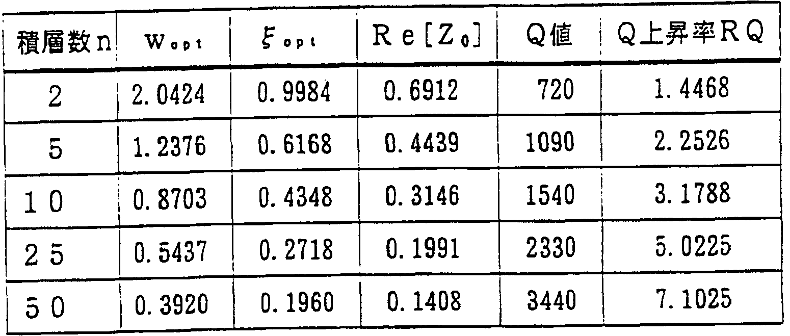
- Fig. 8 shows the simulation results of the 1- and 2-wavelength line type resonators in Fig. 1-a graph showing the frequency characteristics of the transmission coefficient S 21 with the number of layers n as a parameter.
- Fig. 9 is a graph showing the simulation results of the 1- and 2-wavelength line type resonators in Fig. 1, showing the characteristics of the Q increase rate with respect to the normalized conductor film thickness ⁇ (50 with respect to 50) with the number of layers n as a parameter.
- Fig. 1 1 shows the current density distribution of the conductor when high frequency is transmitted to the conductor.
- C Fig. 1 2 shows the ideal current density distribution when high frequency is transmitted to the thin film laminated transmission line of Fig. 1. Is.
- Fig. 13 shows the actual current density distribution when a high frequency is transmitted to the thin film laminated transmission line in Fig. 1.
- Fig. 14 is a flow chart showing the flow for determining the optimum parameters in the 1/2 wavelength line type resonator shown in Fig. 1.
- Fig. 15 is a flow chart showing the determination flow of the minimized surface resistance in the 1 Z 2 wavelength line type resonator of Fig. 1.
- FIG. 16 is a circuit diagram showing an equivalent circuit of a 1/2 wavelength line type resonator filter using an electromagnetic field coupling type thin film laminated transmission line, which is a second embodiment of the present invention. be.
- Fig. 17 is a graph showing the frequency characteristics of the transmission coefficient S 2 1 , which is the simulation result of the 1 2 wavelength line type resonator shown in Fig. 16.
- FIG. 18 is a perspective view of a 1- and 4-wavelength line-type band-stop filter using an electromagnetic field-coupled thin-film laminated transmission line, which is a third embodiment of the present invention.
- Fig. 19 is a circuit diagram including the equivalent circuit of the 14-wavelength line type band-stop filter shown in Fig. 18.
- FIG. 20 shows various microwave lines and waveguides using the electromagnetic field coupling type thin film laminated electrode according to the present invention.
- (a) is the electromagnetic field coupling according to the present invention. It is a perspective view of a microstrip line using a type thin film laminated electrode, (b) is a perspective view of a strip line using an electromagnetic field coupling type thin film laminated electrode according to the present invention, and (c) is a perspective view of the strip line according to the present invention. It is a perspective view of the coaxial line using the electromagnetic field coupling type thin film laminated electrode, and (d) is the longitudinal sectional view of the TM fl i mode circular waveguide using the electromagnetic field coupling type thin film laminated electrode of the present invention. Is.
- FIG. 21 is a schematic cross-sectional view of the 1 Z 2 wavelength line type resonator shown in FIG. 1 in the longitudinal direction.
- Fig. 2 2 is a circuit diagram showing the equivalent circuit of the 4-terminal circuit in Fig. 4.
- Figure 23 is an oblique view showing an example of a modified TM 1 1 C dual-mode dielectric resonator.
- Figure 24 is a new view showing an example of a modified TM 01 4-mode two-stage dielectric bandpass filter.
- Fig. 25 shows the thin film conductors 2 1 and the ground conductors for the transmission distance when the film thickness ⁇ , of the thin film dielectric 3 1 and 3 4 is thinned in the thin film laminated transmission line according to the present invention. It is a graph which shows the effective current value of the current flowing through 1 1.
- Fig. 26 shows the thin film dielectric 3 1 in the thin film laminated transmission line according to the present invention. It is a graph showing the effective current value of the current flowing through each thin film conductor 2 1 and the ground conductor 1 1 with respect to the transmission distance when the film thickness ⁇ ⁇ , of the maximum 34 is increased.
- Fig. 27 shows a modification of the 1/2 wavelength line type resonator using the electromagnetic field integrated thin film laminated transmission line, which is the first embodiment of the present invention, using the thin film laminated transmission line as the ground conductor. It is a cross-sectional view which shows.
- Fig. 28 is a graph showing the relative amplitude value of the current flowing through each thin film conductor 2 1 to 25 and the ground conductor 1 1 with respect to the transmission distance of the 1 Z 2 wavelength line type resonator in Fig. 1. The best mode for carrying out the invention
- FIG. 1 is a perspective view of a filter using a 1 ⁇ two-wavelength line type resonator using an electromagnetic field-coupled thin film laminated transmission line according to the first embodiment of the present invention
- FIG. 2 is a perspective view of a filter. This is a vertical cross-sectional view of the ⁇ —A'line of the 1 ⁇ 2 wavelength line type resonator in Fig. 1.
- the 1-no-two-wavelength line type resonator of the first embodiment has a structure in which thin film conductors 2 1 to 25 and thin film dielectrics 3 1 to 34 are alternately laminated, and is an electromagnetic field according to the present invention. It is characterized by using an electromagnetic field-coupled thin-film laminated transmission line that uses a coupled thin-film laminated electrode.
- the electromagnetic field combined type thin film laminated transmission line the thin film conductor 2 1 and the ground conductor 1 1 and the dielectric substrate 10 sandwiched between the thin film conductor 2 1 and the ground conductor 1 1 are used in TEM mode.
- Microstrip line (hereinafter referred to as the main transmission line) While L 1 is composed, the main transmission line Four TEM mode microstrip lines (hereinafter referred to as sub-transmission lines) L 2 to L 5 in which one thin film dielectric is sandwiched between a pair of thin film conductors on the path L 1 It is laminated.
- sub-transmission lines TEM mode microstrip lines
- the reference number of the transmission line is added after the (comma) for each dielectric of the transmission line.
- each thin film conductor 21 By setting the film thickness ⁇ f of each thin film conductor 21 to 25 to the skin depth of the operating frequency (predetermined film thickness thinner than 0), the above-mentioned adjacent transmission lines L1 and L2. L2 L3. L3 and L4. Each electromagnetic field is coupled to each other at L4 and L5, thereby transferring the high frequency energy flowing through the main fe transmission line L1 to the secondary transmission lines L2 to L5, and each thin film conductor 21 to L5.
- it is configured so that high-frequency currents flow substantially uniformly, and it is characterized by significantly suppressing the epidermis effect due to high frequencies.
- a strip-shaped thin film conductor 21 having a longitudinal length of ⁇ ⁇ 2 (ig is an in-tube wavelength) is formed on a dielectric substrate 10 having a ground conductor 11 formed on the entire back surface. It is formed.
- the thin film conductor 21, the ground conductor 11, and the dielectric base 10 sandwiched between the two conductors 21 and 11 form a main transmission line L 1 composed of a micro stripped line.
- a thin film conductor 31, a thin film conductor 22, a thin film dielectric 32, a thin film conductor 23, a thin film dielectric 33, a thin film conductor 24, a thin film dielectric 34, and a thin film conductor 25 are layered on the thin film conductor 21 in this order. Will be done.
- the sub-transmission lines L 2 to L 5 are configured as follows. (a) The thin film dielectric 31 is sandwiched by a pair of thin film conductors 21. 22 to form the secondary transmission line L 2.
- the thin film dielectric 34 is sandwiched by a pair of thin film conductors 24 and 25 to form the secondary transmission line L 5.
- each thin film conductor 21 to 25 and the film thickness X, of each thin film dielectric 31 to 34 are set as described in detail later using the flow for determining the optimum parameters in FIG.
- the dielectric substrate 10 is formed on the dielectric substrate 10 so as to be separated from one end of the input terminal conductor 12 ⁇ thin film conductor 21 in the longitudinal direction by a predetermined gear g 1 and close to each other so as to be electromagnetically coupled to each other. It is formed so that the output terminal conductor 13 force, the other end of the thin film conductor 21 in the longitudinal direction, and the predetermined gear g 2 are separated from each other and electromagnetically coupled to each other.
- the coupling between the input terminal conductor 12 and one end of the thin film conductor 21 and the coupling between the output terminal conductor 13 and the other end of the thin film conductor 21 are capacitive couplings. ..
- the dielectric substrate 10 is made of, for example, sapphire, which is a single crystal of alumina, and the thin film dielectrics 31 to 34 are made of, for example, S i 0 2 .
- the grounding conductor 11 and the thin film conductors 21 to 25 are conductors having electrical conductivity such as Cu, Ag or Au.
- Figure 2 shows the electric and magnetic field distributions in the 1- and 2-wavelength line type resonators configured as described above.
- Fig. 2 omits the hatching of the dielectric, which is a cross-sectional view.
- the electric fields are distributed in the direction perpendicular to the surface of each thin film conductor 21 to 25 and in the same direction as each other.
- the magnetic fields are distributed in parallel directions to the surfaces of the thin film conductors 21 to 25 and in the same direction as each other.
- C Therefore, the electromagnetic fields of the transmission lines L 1 to L 5 are coupled to each other. I understand.
- Fig. 3 is a schematic cross-sectional view of the 1- and 2-wavelength line type resonators in Fig. 1 and the circuit diagram of the circuit connected to it.
- Fig. 4 is a 1- and 2-wave long line type resonator in Fig. 1. It is a circuit diagram of the equivalent circuit of the vessel.
- the unit distribution constant circuit of the LC is connected in series, and the inductor L11.
- the load resistor R is connected to the other end of the main transmission line L 1 via an ideal transformer T12 having a capacitor ratio corresponding to the gear g 2.
- the ratio of numbers is 1: 1.
- ideal transformers Ti ll, Ding 112.... Ding 11 n are inserted and connected to the lines on the upper and lower sides of the diagram between each unit distribution constant circuit, and each ideal transformer Ti l l.
- Tl 12, ⁇ ⁇ T 11 n is a 4-terminal circuit consisting of a distributed constant circuit including loss resistance F 1, F 2...., F n and an ideal transformer T 10 1, T 102, ⁇ ⁇ ⁇ , T l On It is connected to the earth.
- the following 4-terminal circuit (signed by F + number) is an equivalent circuit of the ground conductor 11 and the thin film conductors 21 to 25, and is a distributed constant circuit including loss resistance as shown in Fig. 22. .. That is, the four-terminal circuit has a unit conductance gd x, a unit capacitance cd X, and a unit binder, respectively.
- a unit circuit consisting of 1 dx is composed of multiple ffi circuits connected in succession, where the unit conductance gd X, the unit capacitance cd, and the unit inductance 1 d X are expressed by the following equations. NS.
- ⁇ is the conductivity of the ground conductor 11 and the thin film conductors 21 to 25
- ⁇ ⁇ is the permittivity in the air
- 0 is the magnetic permeability in vacuum
- d X is the thickness of the ground conductor 11 and the thin film conductors 2 1 to 25.
- the minute length in the vertical direction, is the line width
- dz is the minute length in the propagation direction.
- the sub-transmission line L 2 is equipped with an injector L 21. L 22. ⁇ , L 2 n and a capacitor C 21. C 22. -C 2 n with the unit distribution constant circuit of LC connected in succession. It is composed of a distributed constant circuit, and an ideal transformer T 21 whose primary side is open is connected to one end of its sub-transmission line L 2, while an ideal capacitor T 21 whose secondary side is open is connected to the other end of the sub-transmission line L 2. T 22 is connected.
- the sub-transmission lines L3, L4. L 5 are configured as follows in the same manner as the sub-transmission line L 2.
- the sub-transmission line L 3 consists of a distributed constant circuit in which the unit distribution constant circuit of LC is connected in a longitudinal manner and is equipped with an adapter L31. L 32. ⁇ , L3 n and capacitors C31, C32.
- An ideal transformer T 31 with an open primary side is connected to one end of the sub transmission line L 3, while an ideal transformer T 32 with an open secondary side is connected to the other end of the sub transmission line L 3.
- the sub-transmission line L 4 is a distributed constant circuit with an inductor L 41, L42. To one end of the sub-transmission line L 4, a conceptual capacitor T 41 with an open primary side is connected, while to the other end of the sub-transmission line L 4, the secondary side.
- the ideal transformer T 42 which is open, is attached. Furthermore, the sub-transmission line L 5 is a distributed constant circuit in which the unit distribution constant circuit of LC is connected in series and has an adapter L 51, 152, ⁇ ', L 5n and a capacitor C 51. C 52,... C 5 n.
- An ideal capacitor T51 that is configured and whose primary side is open is connected to one end of its sub-transmission line L 5, while an ideal capacitor T 52 that is open to the secondary side is connected to the other end of the sub-transmission line L 5. Is connected.
- the equivalent circuit in the thin film conductor 21 connecting the adjacent transmission lines L 1 and L 2 is configured as follows. That is, in the main transmission line L 1, the ideal transformers 121. T1 22.... 12 n are inserted and connected to the upper lines in the figure between each unit distribution constant circuit, and each ideal transformer 121. T1227-8 . T12 n is a diagram between each unit distribution constant circuit of the sub-transmission line L 2 via the 4-terminal circuit F 11. F 12. ⁇ F 1 n corresponding to the thin film conductor 21, respectively. Connected to the ideal transformers T 211, T21 2, ⁇ , T21 n, respectively.
- L 3 The equivalent circuit in the thin film conductor 22 connecting the adjacent transmission lines L 2.
- L 3 is configured as follows. That is, in the sub-transmission line L2, the ideal transformers T 221, T222. ⁇ .. ⁇ 22 ⁇ is a 4-terminal circuit corresponding to the thin film conductor 22 F 21, F22, ⁇ . It is connected to the ideal transformer ⁇ 311. ⁇ 3 12. .. ⁇ ⁇ , which is inserted and connected to each line.
- L 4 is configured as follows. That is, in the sub-transmission line L 3, the ideal transformer ⁇ 32 is on the upper line in the figure between each unit distribution constant circuit. 1, T322. To T32 n are inserted and connected, and each ideal transformer is 321. T
- ⁇ . T32n is a diagram between each unit distribution constant circuit of the sub-transmission line L 4 via the 4-terminal circuit F 31, F32, ⁇ . F 3 ⁇ corresponding to the thin film conductor 23, respectively.
- Ideal transformers that are inserted and connected to the upper and lower lines, respectively. 411. ⁇ 412. ⁇ . ⁇ 41 ⁇ is connected.
- the equivalent circuit in the thin film conductor 24 connecting the adjacent transmission lines L 4 and L 5 is configured as follows. That is, in the sub-transmission line L 4, the ideal transformer ⁇ is on the upper line in the figure between each unit distribution constant circuit.
- each ideal transformer ⁇ 421, ⁇ 422...., ⁇ 42 ⁇ is a 4-terminal circuit F41, F42.
- Each unit distribution constant of the sub-transmission line L 4 is inserted and connected to the upper and lower lines of the diagram between the circuits. 51 1. ⁇ 12. ⁇ . ⁇ 5 In.
- the equivalent circuit corresponding to the electromagnetic field distribution formed from the thin film conductor 25 toward the space is configured as follows. That is, in the sub-transmission line L 5, the ideal transformer T is on the upper line in the figure between each unit distribution constant circuit.
- T522 521, T522. ⁇ T52 n are inserted and connected, and each ideal transformer 521.
- T522, ⁇ , T52n is a 4-terminal circuit corresponding to the thin film conductor 25 F51 .. F52. ⁇ F5n and ideal transformer, respectively.
- T531, T532, ⁇ Connected to the load resistors R L1 , R L2 .. ⁇ . Through T53 n.
- ⁇ 5 Permittivity of thin film dielectrics 31 to 34 of sub-transmission line L 2 to L 5 ⁇ m : Dielectric constant of dielectric substrate 10 of main transmission line L 1
- the subscript k of the complex impedance ⁇ has the main transmission line L1 as the 0th, and the sub-transmission lines L 2 to L in the upper layer. Shows the line numbers numbered in ascending order towards 5.
- the complex impedance Z and the complex admittance Y are defined by the functions expressed by the following equations (2) and (3), respectively, with the medium parameter ⁇ as a variable.
- Figure 14 shows the optimum parameter Wop in the 1Z2 wavelength line type resonator according to the present invention. It is a flowchart which shows the decision flow of.
- step S1 the n-layer recurrence formula (1) is determined based on the predetermined number of layers n. Then, the following decisions are made based on the n-layer recurrence formula.
- step S2 the optimal structural parameter w is based on an optimization that matches the phase velocity ⁇ of each TEM wave propagating along each transmission line L1 through L5. Determine Pl. Then, in step 3, the film thickness ⁇ x. Of the thin film dielectrics 31 to 34 of the sub-transmission lines L 2 to L 5 is determined based on Equation 9.
- step S4 the optimal structural parameter f is based on the optimization of the energy coupling. Determine Pt.
- step 5 the film thickness ⁇ of the thin film conductors 21 to 25 is determined based on Equation 10.
- the real part of (w. ⁇ ) Re [Z. (W. F)] is obtained as the minimum structural parameter w and the medium parameter, and these are optimized structural parameters w. P and medium parameter f. And.
- FIG. 15 is a flow chart showing the flow of determining the minimized surface resistance R s in the 12-wavelength line type resonator according to the present invention.
- step S11 the optimal structural parameter w, as shown in Figure 15. And the optimum medium parameter f. And then Re [Z based on the n-layer recurrence formula (1). (W ...)] is determined.
- step S12 the decision is made in step S11.
- the conductivity of the thin film conductors 2 1 to 25, and the skin depth S o into equation (8), the minimized surface resistance R s can be obtained. decide.
- the effective permittivity of the thin-film dielectrics 3 1 to 34 constituting the sub-transmission lines L 2 to L 5 is preferably the effective permittivity of the dielectric substrate 10 constituting the main transmission line L 1.
- the phase velocity of the electromagnetic wave propagating on the main transmission line L 1 and the phase velocity of the TEM wave propagating on at least one of the sub transmission lines L 2 to L 5 are more substantially matched with each other. Can be made.
- the thickness of the thin film dielectrics 3 1 to 34 constituting the sub transmission lines L 2 to L 5 is set to be thinner than the thickness of the dielectric substrate 10 constituting the main transmission line L 1. do.
- the time required for the film formation process of the sub-transmission lines L 2 to L 5 can be shortened, and the sub-transmission lines L 2 to L 5 have a smaller impedance. Therefore, the transmission loss can be reduced.
- the permittivity of the thin film dielectrics 3 1 to 34 is given in advance to determine the film thickness X, which is determined by the present invention.
- Eq the permittivity of the thin film dielectrics 3 1 to 34
- the film thickness A x of the thin film dielectrics 3 1 to 34 may be given in advance to determine the permittivity ⁇ ,. Since it is assumed that the electromagnetic field is uniform in the width direction of the transmission line L 1 7 3 ⁇ 4 to L 5, the substrate thickness of the dielectric substrate 10 of the main transmission line L 1 is ⁇ and the line width-thin film. Width of conductors 2 1 to 25-Width of thin film dielectric 3 1 to 34 does not affect the film thickness determination of the above optimization.
- Fig. 5 is a graph showing the frequency characteristics of the transmission coefficient S 21
- Fig. 6 shows the frequency characteristics of the relative amplitude of the lightning current flowing through each thin film conductor 21 to 25 of the 1 2 wavelength line type resonator in Fig. 1.
- I 1 to I 5 are relative amplitude values of the currents flowing through the thin film conductors 21 to 25, respectively.
- Fig. 7 is a graph showing the frequency characteristics of the phase difference of the current flowing through each thin film conductor 21 to 25 of the 1 2 wavelength line type resonator in Fig. 1, and here, in Fig. 7, P 1 and P 5 is the phase difference of the current flowing through the thin film conductors 21 and 25, respectively.
- each parameter in the simulation was set as follows.
- the relative amplitude value of the current flowing through each of the thin film conductors 21 to 25 is maximum at the resonance frequency of 200 OMH z, and the relative amplitude value of the current flowing through the thin film conductors 21 to 25 at that resonance frequency. Declined from the thin film conductor 21 to the thin film conductor 2.5. At the same time, the high-frequency electromagnetic field energy flowing through the main transmission line L 1 is a thin film with loss. It migrates to the thin film dielectrics 31 to 34 via the bodies 21 to 24.
- the phase difference of the 3 ⁇ 4 currents flowing through the thin film conductors 21 to 25 at the resonance frequency of 2000 MHz is 0 ⁇ and matches, and the frequency is approximately ⁇ 90 ° at the frequency of 1990. 201 ⁇ . It has become.
- Fig. 8 is a graph showing the frequency characteristics of the transmission coefficient S 21 with the number of layers ⁇ as a parameter, which is the simulation result of the 1/2 wavelength line type resonator in Fig. 3, and Fig. 9 shows the number of layers ⁇ . It is a graph showing the parameter and the normalized conductor film thickness ⁇ / ⁇ to Q increasing rate RQ characteristic, FIG. 10, the effective dielectric constant ratio the laminated number ⁇ as a parameter £, Z £ m vs. normalized dielectric film thickness It is a graph that shows 0 characteristics.
- each parameter in the simulation was set as follows.
- the ground conductor 11 was set as a perfect conductor in order to evaluate only the thin film laminated electrodes in the simulation. In reality, this corresponds to the structure when a mirror image is drawn with the interface with the perfect conductor as the plane of symmetry. That is, the thickness of the attractant substrate 10 is doubled to form thin film laminated electrodes on both sides thereof. Corresponds to the model.
- Figure 10 shows the optimal parameters w in Table 1. This is the result of calculating the relationship between the standardized dielectric film thickness ⁇ , ⁇ (5o and the effective permittivity ratio ⁇ , Z £ m) based on the formula obtained when the value of is substituted into equation (4). , As is clear from Fig. 10, the effective permittivity ratio of the main transmission line L 1 and the sub transmission lines L 2 to L 5
- each thin film conductor 21 to 25 By setting the film thickness of each thin film conductor 21 to 25 to a predetermined film thickness thinner than the skin depth ⁇ 50 of the operating frequency, L1 and L2, L2 and L3 between the adjacent transmission lines mentioned above. . L3 and L4, L4 and L5 couple each electromagnetic field to each other, thereby transferring the high frequency energy flowing in the main transmission line L1 to the secondary transmission lines L2 to L5, and each thin film conductor 21 to At 25, each of them is configured so that a high-frequency current flows substantially uniformly, and the skin effect due to the high frequency is greatly suppressed.
- Fig. 21 is a schematic cross-sectional view of the 1- to 2-wavelength line type resonator shown in Fig. 1 in the longitudinal direction, and is drawn with the longitudinal direction significantly shortened compared to the thickness direction. ing.
- the high-frequency current is shown by the solid line and the displacement current is shown by the dotted line.
- each of the thin-film conductors 21 to 25 When excited by a high-frequency signal on the main transmission line L1, each of the thin-film conductors 21 to 25 receives a part of the high-frequency power incident through the lower thin-film dielectric on the upper side, as shown in Fig. 21.
- part of the energy of the high frequency signal is reflected to the lower thin film conductor via the lower thin film dielectric.
- the reflected wave and the transmitted wave resonate in each of the thin film dielectrics 31 to 34 sandwiched between two adjacent thin film conductors, and the reflected wave and the transmitted wave resonate with each other near the upper surface and the lower side of each of the conductor thin films 21 to 25.
- frequency current Two high-frequency currents facing each other in opposite directions near the surface (hereinafter, two highs facing each other) It is called frequency current. ) Is flowing. That is, since the film thickness of the core conductors 2 1 to 25 is thinner than the skin depth ⁇ 0, the two high-frequency currents facing each other in opposite directions are partially squeezed through the thin film dielectric. Are offset by each other, leaving behind.
- a displacement current is generated by an electromagnetic field, and a high frequency current is generated on the surface of an adjacent thin film conductor.
- the displacement current is maximum at both ends of the line in the longitudinal direction and minimum at the center.
- the film thickness X which determines the effective permittivity of each thin-film dielectric 3 1 to 34, and the permittivity ⁇ t , and the phase velocity of the TEM wave propagating in each transmission line L 1 to L 5 are substantially determined. Since they are set to be identical to each other, the high-frequency currents flowing through the thin film conductors 2 1 to 25 are substantially in phase with each other. As a result, the high-frequency current flowing in the same phase in each thin film conductor 21 to 25 effectively increases the skin depth 50.
- the resonator when the resonator is excited by a high-frequency signal, the high-frequency electromagnetic field energy is transferred to a higher transmission line by competing with the electromagnetic fields of the adjacent transmission lines, while the transmission line of the resonator is transferred. Propagate in the longitudinal direction of. At this time, the resonator has an effective larger skin depth ⁇ 50, in other words, a smaller surface resistance R, and the TEM wave propagates through the 1 Z 2 wavelength line. Since it is reflected at both ends of the road, it becomes a resonance state.
- Fig. 28 is a graph showing the relative amplitude values of the currents flowing through the thin film conductors 21 to 25 and the ground conductor 11 with respect to the transmission distance of the 1- and 2-wavelength line type resonators in Fig. 1.
- each parameter in the simulation is as follows.
- Ig and I 1 to I 5 are the relative amplitude values of the current flowing through the ground conductor 11 and the thin film conductors 21 to 25, respectively.
- the currents flowing through the ground conductors 11 and the thin film conductors 21 to 25 are divided at a constant rate, and each of them constitutes a standing wave.
- the resonator of this embodiment has the following unique advantages.
- the line impedance can be changed without changing the line width by using or not using a thin film laminated transmission line or by changing the number of layers thereof. .. Therefore, the pattern design on the dielectric substrate becomes easy.
- ground conductor 1 1 of the above first embodiment may be made into the above-mentioned high-circumferential electromagnetic field coupling type thin film laminated electrode structure, and the remaining conductors may be left as the conventionally known structure, or the ground conductor 1 1 may also be used.
- the above-mentioned high-frequency electromagnetic field-coupled thin film layered electrode structure may be used.
- thin film conductor 2 a thin film conductor 2 3 a, thin film dielectric 3 3 a, thin film conductor 2 4 a, thin film dielectric
- a protective dielectric may be formed on the top layer thin film conductor 25 of the first embodiment and the thin film conductor 25 a of the modification of the first embodiment described above, or the resonator may be formed. It may be formed so as to surround the whole with a protective conductor.
- the main transmission line L 1 and each sub transmission line L 2 to L 5 are microphone ⁇ strip lines, but the present invention is not limited to this, and the tribrate type strip line and the cobrena It may be a transmission line such as a line or a slot line.
- the thin film laminated conductor according to the present invention may be used for at least one of the center conductor and the ground conductor.
- the thicknesses of the thin film dielectrics 3 1 to 34 are X so that the phase velocities of the TEM waves propagating on the transmission lines L 1 to L 5 are substantially matched with each other.
- the phase velocities of the waves may be configured to substantially match each other.
- the sub-transmission lines L 2 to L 5 may be configured to include at least one.
- the electromagnetic fields are coupled to each other at L 1 and L 2, L 2 and L 3, L 3 and L 4, L 4 and L 5 between the adjacent transmission lines.
- the force that sets the film thickness ⁇ f of each thin vaginal conductor 2 1 to 25 ⁇ the present invention is not limited to this, and of the main transmission line L 1 and the sub transmission lines L 2 to L 5
- the electromagnetic fields may be configured to be coupled to each other with at least one.
- the main transmission line L 1 is the force used as the transmission line of the T EM mode.
- the present invention is not limited to this, and the main transmission line L 1 is in TE mode or TM mode. It may be a transmission line that propagates electromagnetic waves.
- the force described for the filter using the electromagnetic field-coupled thin-film laminated £ transmission line L and the 1/2 wavelength line type resonator is based on this.
- a filter using a 1- to 4-wavelength line-type resonator using an electromagnetic field-coupled thin-film laminated transmission line may be configured.
- the electromagnetic field is coupled by relatively strong electromagnetic coupling between the input transmission line and the electromagnetic field-coupled thin-film laminated transmission line, and between the output transmission line and the electromagnetic field-coupled thin-film laminated transmission line.
- a coupled thin film laminated transmission line can be used as a transmission line with extremely low loss.
- Fig. 25 shows the thin film dielectric 3 1 in the thin film laminated transmission line according to the present invention. Effectiveness of the current flowing through each thin film conductor 21 to 25 and ground conductor 11 with respect to the transmission distance from the input end when the thickness x, of up to 34 is reduced from 0.73 / m to 0.36 // m. It is a graph showing the current value, and Fig. 26 shows the input when the thickness ⁇ , of the thin film dielectrics 31 to 34 is increased from 0.73 / zm to 1.37 m in the thin film laminated transmission line according to the present invention. It is a graph showing the effective current value of the current flowing through each thin film conductor 21 to 25 and the ground conductor 11 with respect to the transmission distance from the end.
- each parameter in the simulation was set as follows.
- I gb, I ib, I 2 b. 1 3 b. 1 4 b and I 5 b respectively, have a relative permittivity of 5.2 for the thin film dielectrics 31 to 34 and their films' This is the effective current value of the current flowing through the dielectric conductor 11 and the thin film conductors 21 to 25 when the thickness is 1.37 m.
- Fig. 25 and Fig. 26 only the main transmission line L 1 is excited at the input end, and as the microwave signal propagates, the current penetrates into the sub transmission lines L 2 to L 5 as well.
- FIG. 16 is a circuit diagram showing an equivalent circuit of a 1/2 wavelength line type resonator filter using an electromagnetic field coupling type thin film laminated transmission line, which is the second embodiment of the present invention.
- the conceptual transformers Ti l, T21.' ⁇ , T 51 connected to each transmission line L 1 to L 5, respectively.
- the primary side is connected in series and its A series circuit of the signal generator V sg and its internal resistance R sg is connected to both ends.
- the secondary side of the ideal transformer T 1 2. T 2 2. ⁇ , T 5 2 on the other end side is connected in series, and the load resistor R L is connected to both ends.
- Fig. 17 is a graph showing the frequency characteristics of the transmission coefficient S 21 , which is the simulation result of the 1- and 2-wavelength line type resonators in Fig. 16. Here, each parameter in the simulation was set in the same manner as in Fig. 5.
- each transmission line L 1 to L 5 may be weighted and excited by using a variable amplifier or a variable attenuator and an in-phase distributor. In this case, the distribution of the propagating electromagnetic field energy in each transmission line L 1 to L 5 can be changed.
- FIG. 18 is a perspective view of a 1/4 wavelength line type band stop filter using an electromagnetic field coupling type thin film laminated transmission line according to the third embodiment of the present invention.
- the microstrib line L is formed by forming the microstrib conductor 4 1 on the dielectric substrate 10 in which the ground conductor 1 1 is formed on the entire back surface. 10 is formed. Then, the thin film laminated electrode of the first embodiment, which includes each thin film conductor 2 1 to 25 and each thin film dielectric 3 1 to 3 4 and has a length of 1 4 ⁇ g, is a microstrip line L 1 0.
- FIG. 19 is a circuit diagram including an equivalent circuit of the 1Z4 wavelength line type band-stop filter of FIG.
- the microscopic lip line L 10 has an inductor L 100. L 101. ⁇ , L 1 On, L 10 (n + 1) and capacitors C 100, C 101, ⁇ , C 10 n. Consists of a distributed constant circuit with CI O (n + 1), and a resonator excitation at one end of the micro strip line L 10
- the V sg of the signal generator and its internal resistance R sg are connected, while the load resistance R L is connected to the other end of the microstrib line L 10.
- T61 (n + 1) are inserted and connected to the lines on the upper and lower sides of the figure between each unit distribution constant circuit, and each ideal transformer is connected.
- T 610, T611. ⁇ . T61 n. T61 (n + 1) is a 4-terminal circuit F60. F61, ⁇ , F 6 n. F 6 (n + 1) and ideal transformer T60 0. T601. ⁇ ⁇ . Connected to ground via T6 On. T60 (n + 1).
- the gap g 3 causes inductive coupling and capacitive coupling as follows. Inductively coupled M between Inductor L 11 and L 101 L 1 2 and LI 0 2 are inductively coupled M, and in the same manner, the inductors L 1 n and L 10 n are inductively coupled M. In addition, the capacitors C 1 1 and C 1 0 1 are capacitively coupled, the capacitors C 1 2 and C 1 0 2 are capacitively coupled, and so on. Capacitively coupled.
- a resonator with extremely small conductor loss can be constructed by using a thin film product transmission line of 1 to 4 wavelength lines, so a microstrike that is electromagnetically coupled to it can be constructed. By forming the line L 10 it is possible to construct a 1 Z 4 wavelength line type band elimination filter having an extremely large no-load Q.
- the micro strip line L 10 is used, but the present invention is not limited to this, and is composed of a transmission line such as a cobrena line, a slot line, or a triplate type strip line. You may. Modification example
- the surface resistance of the electrode is significantly reduced as compared with the conventional case, and thereby the transmission loss is significantly reduced. Can be made smaller.
- FIG. 20 (a) is a perspective view of a micro-tribut line using the electromagnetic field-coupled thin film laminated electrode according to the present invention, and is a micro-tribut conductor 5 1 and a ground conductor 5 2 of the micro strut line.
- Use an electromagnetic field-coupled thin film laminated electrode An electromagnetic field-coupled thin film laminated electrode may be used only for the microstrip conductor 51, or an electromagnetic field coupled thin film laminated electrode may be used only for the ground conductor 5 2.
- FIG. 20 (b) is a perspective view of a rib rate type strip line using the electromagnetic field coupling type thin film laminated electrode according to the present invention.
- Electromagnetic field-coupled thin-film laminated electrodes are used for the micro strip conductors 6 1 and the ground conductors 6 2 and 6 3.
- An electromagnetic field-coupled thin-film laminated electrode may be used only for the micro-trip conductor 61, or an electromagnetic-field-coupled thin-film laminated electrode may be used for at least one of the ground conductors 6 2.6 3. good.
- FIG. 20 (c) is a perspective view of a coaxial line using the electromagnetic field coupling type thin film laminated electrode according to the present invention, and is electromagnetically coupled to the central conductor 7 1 and the ground conductor 7 2 of the coaxial line.
- a mold thin film laminated electrode is used.
- An electromagnetic field coupling type thin film stacking electrode may be used only for the center conductor 7 1, or an electromagnetic field coupling type thin film laminated electrode may be used only for the ground conductor 7 2.
- FIG. 20 (d) is a cross-sectional view of a TM D 1 mode circular waveguide using the electromagnetic field coupling type thin film laminated electrode 73 according to the present invention, and is a cross-sectional view of the circular waveguide.
- An electromagnetic field-coupled thin film laminated electrode is used as the outer surface electrode.
- an electromagnetic field-coupled thin film laminated cocoon electrode may be used for the outer surface electrode of the rectangular waveguide (not shown).
- the electromagnetically coupled thin film laminated electrode according to the present invention is, for example, published in Japan Patent Publication No. 1991 (1991) No. 2 9 2 0 0 6 (Patent application in Japan 1990 (1 9)).
- the M-mode dielectric resonator is not limited to the TM-mode single-mode type described above. It can be applied to a dual-mode dielectric resonator (see, for example, Fig. 23) as disclosed in the application No. 1500 0 2 1 in 1987. Furthermore, the publication of the patent in Japan, 1986, was published in 1 5 7 1 0 1 (patent application in Japan, 1984, 2 7 9 2 0 3).
- Figure 23 shows an example of a modified example of the dual-mode dielectric resonator 75.
- a square tubular resonator case 7 7 with a metallized outer surface of the dielectric is provided with a cross-shaped dielectric 7 6 integrally molded with the case 7 7 in the center of the case 7 7 to provide a double-mode dielectric resonance.
- Vessel 7 5 is configured.
- the electrode of the resonator case 77 the electromagnetic field coupling type thin film laminated electrode according to the present invention is used as the electrode of the resonator case 77. As a result, the surface resistance of the electrode can be significantly reduced, so that the loss of the dielectric resonator can be reduced and the no-load Q can be increased.
- FIG 24 shows an example of a modified TMo mode type two-stage electric body bandpass filter 80.
- the bandpass filter 80 is configured as follows. S MA connectors 8 3. 8 4 for input and output are attached to both ends of a cylindrical dielectric tube 8 1 having outer peripheral electrodes 8 2, where the S MA connector 8 3. 8 4 is grounded. The conductors are connected to the outer peripheral electrodes 8 2, while the central conductors of the S MA connector 8 3.8 4 are connected to the monopole antennas 8 5, 8 6 facing each other in the dielectric tube 81, respectively. ..
- a ring-shaped dielectric support base 8 9.9 that is inscribed in the inner peripheral surface of the dielectric tube 8 1 at a predetermined interval within the dielectric tube 8 1 between the monopole antennas 8 5 and 8 6.
- the outer peripheral electrode 82 has the electromagnetic field-coupled thin film laminate and poles according to the present invention. As a result, the surface resistance of the outer peripheral electrode 82 can be significantly reduced, so that the loss of the dielectric filter can be reduced and the no-load Q can be increased.
- inductors such as isolators, antennas, chip coils, and carriers.
- the electromagnetic field-coupled thin film laminated electrode according to the present invention can be used for one pole of various high-frequency devices such as a pasita that perform predetermined high-frequency operations.
- the solid thin film dielectrics 31 to 34 are used, but the present invention is not limited to this, and a gas or liquid such as air may be used instead of the thin film dielectrics 31 to 34.
- the thin film dielectrics 31 to 34 have the same film thickness, but the present invention is not limited to this, and the film thicknesses of the thin film dielectrics 31 to 34 are set to be different. May be good.
- the thin film conductors 21 to 24 have the same film thickness, but the present invention is not limited to this, and the film thicknesses of the thin film conductors 21 to 24 may be set differently.
- the ground conductor 11 and the thin film conductors 21 to 25 are, for example, conductors having electrical conductivity such as Cu, Ag, or Au, but the present invention is not limited to this, and the ground conductor is not limited to this.
- 11 and thin-film conductors 21 to 25 may use the following superconductors (superconductors) as at least one material.
- B i— S r— Ca— Cu— 0 series where the B i— S r— C a— Cu— 0 series superconducting materials are B i 2 0 3 , S rC 0 3 , CaC0 3 and It is obtained by calcining a powder mixed with CuO at a temperature of 800 to 870 ° C and then sintering it in the air at a temperature of 850 to 880 ° C.
- TTSF Tetramethyltetraselenafulvalene
- the thin film dielectric (3 1 1 3 4) is sandwiched by alternately laminating the thin film conductor (21-25) and the thin film inducer (31–34).
- Thin film lamination consisting of multiple T EM mode transmission lines (L2—L5) composed of a pair of the above thin film conductors (21 and 22. 22 and 23. 2 3 and 24. 24 and 25), respectively.
- each TEM wave is substantially matched to each other, and the film thickness of each thin film conductor (2 1–25) is made thinner than the skin depth of the frequency used, so that the multiple TEM mode transmission lines ( At least two electromagnetic fields of L 2—; L 5> are set to combine with each other, thus effectively increasing the skin depth, thereby compared to conventional structures.
- Conductor loss and surface resistance can be significantly reduced as compared with the conventional one without substantially increasing the external dimensions.
- a high circumference with a smaller transmission loss can be used.
- wave transmission line, a very large unloaded Q RF resonator or a high-frequency filter or a high frequency device it can be achieved by smaller and lighter c
Landscapes
- Chemical & Material Sciences (AREA)
- Engineering & Computer Science (AREA)
- Ceramic Engineering (AREA)
- Physics & Mathematics (AREA)
- Electromagnetism (AREA)
- Control Of Motors That Do Not Use Commutators (AREA)
Description
Claims
Priority Applications (10)
| Application Number | Priority Date | Filing Date | Title |
|---|---|---|---|
| KR1019960700975A KR100285018B1 (ko) | 1993-08-27 | 1994-03-07 | 고주파 전자계 결합형 박막 적층 전극 |
| DE69428801T DE69428801T2 (de) | 1993-08-27 | 1994-03-07 | Dünnfilm mehrschichtelektrode zur kopplung von hochfrequenten elektromagnetischen feldern |
| CA002170270A CA2170270C (en) | 1993-08-27 | 1994-03-07 | Thin film multilayered electrode of high frequency electromagnetic field coupling |
| US08/604,952 US6148221A (en) | 1993-08-27 | 1994-03-07 | Thin film multilayered electrode of high frequency electromagnetic field coupling |
| BR9407631A BR9407631A (pt) | 1993-08-27 | 1994-03-07 | Electrodo de camadas múltiplas de filme fino de acoplamento com campo eletromagnético de alta frequenica |
| EP94908501A EP0716468B1 (en) | 1993-08-27 | 1994-03-07 | Thin-film multilayer electrode of high frequency electromagnetic field coupling |
| RU96108787A RU2139613C1 (ru) | 1993-08-27 | 1994-03-07 | Тонкопленочный многослойный электрод, связанный по высокочастотному электромагнитному полю, высокочастотная линия передачи, высокочастотный резонатор, высокочастотный фильтр, высокочастотный полосовой режекторный фильтр и высокочастотное устройство |
| AU61566/94A AU677380B2 (en) | 1993-08-27 | 1994-03-07 | Thin-film multilayer electrode of high frequency electromagnetic field coupling |
| JP07507463A JP3089666B2 (ja) | 1993-08-27 | 1994-03-07 | 高周波伝送線路、高周波共振器、高周波フィルタ及び高周波帯域除去フィルタ |
| FI960901A FI118360B (fi) | 1993-08-27 | 1996-02-27 | Monikerroksinen ohutkalvoelektrodi, jossa on suurtaajuisen sähkömagneettisen kentän kytkentä |
Applications Claiming Priority (2)
| Application Number | Priority Date | Filing Date | Title |
|---|---|---|---|
| JP5/212630 | 1993-08-27 | ||
| JP21263093 | 1993-08-27 |
Publications (1)
| Publication Number | Publication Date |
|---|---|
| WO1995006336A1 true WO1995006336A1 (fr) | 1995-03-02 |
Family
ID=16625852
Family Applications (1)
| Application Number | Title | Priority Date | Filing Date |
|---|---|---|---|
| PCT/JP1994/000357 WO1995006336A1 (fr) | 1993-08-27 | 1994-03-07 | Electrode multicouche a couches minces utilisee pour le couplage de champs electromagnetiques a hautes frequences |
Country Status (12)
| Country | Link |
|---|---|
| US (1) | US6148221A (ja) |
| EP (1) | EP0716468B1 (ja) |
| JP (1) | JP3089666B2 (ja) |
| KR (1) | KR100285018B1 (ja) |
| CN (1) | CN1122327C (ja) |
| AU (1) | AU677380B2 (ja) |
| BR (1) | BR9407631A (ja) |
| CA (1) | CA2170270C (ja) |
| DE (1) | DE69428801T2 (ja) |
| FI (1) | FI118360B (ja) |
| RU (1) | RU2139613C1 (ja) |
| WO (1) | WO1995006336A1 (ja) |
Cited By (10)
| Publication number | Priority date | Publication date | Assignee | Title |
|---|---|---|---|---|
| EP0812025A1 (en) * | 1996-06-03 | 1997-12-10 | Murata Manufacturing Co., Ltd. | Multi-layer thin-film electrode, high-frequency transmission line, high-frequency resonator, and high-frequency filter |
| US5770988A (en) * | 1995-08-23 | 1998-06-23 | Murata Manufacturing Co., Ltd. | Thin-film multilayered electrode and method of fabricating same |
| US5920244A (en) * | 1996-01-23 | 1999-07-06 | Murata Manufacturing Co., Ltd. | Thin-film multilayered electrode, high-frequency resonator, and high-frequency transmission line |
| JP2001211010A (ja) * | 1999-11-16 | 2001-08-03 | Murata Mfg Co Ltd | 平衡−不平衡変換回路、平衡−不平衡変換器および通信機 |
| JP2007525032A (ja) * | 2004-02-27 | 2007-08-30 | セントレ ナショナル デ ラ レチャーチェ シャーティフィック | 同調可能なインダクタンス特性を有する薄層型超伝導体部品、同超伝導体部品の製造方法及び同超伝導体部品を含んだデバイス |
| JP2008527732A (ja) * | 2005-01-17 | 2008-07-24 | セントレ ナショナル デ ラ レチャーチェ シャーティフィック | 積み重ねられた薄層状の超伝導素子を可変インダクタンスとして使用する方法,同素子を含んだデバイス及び同素子のコントロール方法 |
| WO2013147268A1 (ja) * | 2012-03-31 | 2013-10-03 | 独立行政法人国立高等専門学校機構 | 伝送線路及び配線基板、並びに、これらを用いた高周波装置 |
| WO2016018532A1 (en) * | 2014-08-01 | 2016-02-04 | The Penn State Research Foundation | Antenna apparatus and communication system |
| JP2018174591A (ja) * | 2012-05-01 | 2018-11-08 | ナノトン, インコーポレイテッド | 無線周波数(rf)伝導媒体 |
| JPWO2021106443A1 (ja) * | 2019-11-29 | 2021-06-03 |
Families Citing this family (72)
| Publication number | Priority date | Publication date | Assignee | Title |
|---|---|---|---|---|
| JP3125618B2 (ja) * | 1995-03-27 | 2001-01-22 | 株式会社村田製作所 | 超電導多層電極、超電導多層電極を用いた高周波伝送線路、高周波共振器、高周波フィルタ、高周波デバイス及び超電導多層電極の設計方法 |
| JP3085205B2 (ja) * | 1996-08-29 | 2000-09-04 | 株式会社村田製作所 | Tmモード誘電体共振器とこれを用いたtmモード誘電体フィルタ及びtmモード誘電体デュプレクサ |
| JP3405140B2 (ja) * | 1996-12-11 | 2003-05-12 | 株式会社村田製作所 | 誘電体共振器 |
| JPH11177310A (ja) * | 1997-10-09 | 1999-07-02 | Murata Mfg Co Ltd | 高周波伝送線路、誘電体共振器、フィルタ、デュプレクサおよび通信機 |
| JPH11312910A (ja) * | 1998-04-28 | 1999-11-09 | Murata Mfg Co Ltd | 誘電体共振器、誘電体フィルタ、誘電体デュプレクサおよび通信機装置ならびに誘電体共振器の製造方法 |
| JP3391272B2 (ja) * | 1998-09-01 | 2003-03-31 | 株式会社村田製作所 | 高周波用低損失電極 |
| JP2000295030A (ja) * | 1999-04-06 | 2000-10-20 | Nec Corp | 高周波装置およびその製造方法 |
| JP2001196817A (ja) | 1999-11-05 | 2001-07-19 | Murata Mfg Co Ltd | 誘電体共振器、誘電体フィルタ、誘電体デュプレクサおよび通信装置 |
| JP3478244B2 (ja) * | 2000-05-25 | 2003-12-15 | 株式会社村田製作所 | 同軸共振器、フィルタ、デュプレクサおよび通信装置 |
| CN1384985A (zh) * | 2000-08-30 | 2002-12-11 | 三菱电机株式会社 | 高频线路及高频电路 |
| US7103525B2 (en) * | 2000-09-08 | 2006-09-05 | Fujitsu Limited | Method of and system for high-frequency-corresponding simulation, and computer product |
| US7884666B1 (en) | 2000-10-11 | 2011-02-08 | Silicon Laboratories Inc. | Method and apparatus for reducing interference |
| DE10147109A1 (de) * | 2001-09-25 | 2003-04-30 | Siemens Ag | Leiter und Basismaterial für Leiterplatten mit reduziertem Skineffekt |
| JP2003174306A (ja) * | 2001-09-27 | 2003-06-20 | Murata Mfg Co Ltd | 共振器、フィルタ、デュプレクサ、および高周波回路装置 |
| JP4370838B2 (ja) * | 2002-08-21 | 2009-11-25 | 株式会社村田製作所 | ノイズフィルタ |
| JPWO2004091035A1 (ja) * | 2003-04-04 | 2006-07-06 | 日本電気株式会社 | 広帯域回路 |
| FR2858463B1 (fr) * | 2003-07-28 | 2007-08-24 | Centre Nat Rech Scient | Procede et systeme de realisation de composants inductifs supraconducteurs en couches minces, et dispositifs incluant de tels composants |
| US7026886B2 (en) * | 2003-10-09 | 2006-04-11 | National Chiao Tung University | Miniaturized microwave integrated circuit using complementary conducting surfaces |
| DE102005056602B4 (de) * | 2005-11-28 | 2008-10-02 | Siemens Ag | Resonator für Magnetresonanzanwendungen |
| WO2007114391A1 (ja) * | 2006-03-31 | 2007-10-11 | Kyocera Corporation | 誘電体導波路デバイス、これを備える移相器、高周波スイッチおよび減衰器、ならびに高周波送信器、高周波受信器、高周波送受信器およびレーダ装置、アレイアンテナ装置、誘電体導波路デバイスの製造方法 |
| DE102006017438B4 (de) * | 2006-04-13 | 2008-09-18 | Siemens Ag | Resonator für Magnetresonanzanwendungen |
| JP5062576B2 (ja) * | 2006-07-31 | 2012-10-31 | 国立大学法人京都大学 | 表皮効果に起因する損失を抑制可能な導波管及び共振器 |
| US8410863B2 (en) * | 2008-07-15 | 2013-04-02 | Panasonic Corporation | Slow wave transmission line |
| EP4234001A3 (en) | 2009-03-09 | 2023-10-18 | NuCurrent, Inc. | System and method for wireless power transfer in implantable medical devices |
| US9300046B2 (en) | 2009-03-09 | 2016-03-29 | Nucurrent, Inc. | Method for manufacture of multi-layer-multi-turn high efficiency inductors |
| US9232893B2 (en) | 2009-03-09 | 2016-01-12 | Nucurrent, Inc. | Method of operation of a multi-layer-multi-turn structure for high efficiency wireless communication |
| US11476566B2 (en) | 2009-03-09 | 2022-10-18 | Nucurrent, Inc. | Multi-layer-multi-turn structure for high efficiency wireless communication |
| US9439287B2 (en) | 2009-03-09 | 2016-09-06 | Nucurrent, Inc. | Multi-layer wire structure for high efficiency wireless communication |
| US9444213B2 (en) | 2009-03-09 | 2016-09-13 | Nucurrent, Inc. | Method for manufacture of multi-layer wire structure for high efficiency wireless communication |
| US9208942B2 (en) * | 2009-03-09 | 2015-12-08 | Nucurrent, Inc. | Multi-layer-multi-turn structure for high efficiency wireless communication |
| US9306358B2 (en) | 2009-03-09 | 2016-04-05 | Nucurrent, Inc. | Method for manufacture of multi-layer wire structure for high efficiency wireless communication |
| GB201018646D0 (en) * | 2010-11-04 | 2010-12-22 | Era Tech Ltd | Artificial planar conductor using nano engineered metal films |
| US9564672B2 (en) | 2011-03-22 | 2017-02-07 | Intel Corporation | Lightweight cavity filter structure |
| US9312594B2 (en) | 2011-03-22 | 2016-04-12 | Intel Corporation | Lightweight cavity filter and radio subsystem structures |
| RU2469280C1 (ru) * | 2011-05-24 | 2012-12-10 | Учреждение Российской академии наук Институт радиотехники и электроники им. В.А. Котельникова РАН | Низкотемпературный перестраиваемый источник излучения черного тела |
| US20130068499A1 (en) * | 2011-09-15 | 2013-03-21 | Nucurrent Inc. | Method for Operation of Multi-Layer Wire Structure for High Efficiency Wireless Communication |
| US9731603B2 (en) * | 2012-04-19 | 2017-08-15 | GM Global Technology Operations LLC | Electric and hybrid vehicle high current conductor |
| RU2522860C2 (ru) * | 2012-10-04 | 2014-07-20 | Российская Федерация, от имени которой выступает Государственная корпорация по атомной энергии "Росатом" | Устройство для одновременной трансляции сигналов в оптическом и радиочастотном диапазонах излучения |
| US9570222B2 (en) | 2013-05-28 | 2017-02-14 | Tdk Corporation | Vector inductor having multiple mutually coupled metalization layers providing high quality factor |
| US9324490B2 (en) | 2013-05-28 | 2016-04-26 | Tdk Corporation | Apparatus and methods for vector inductors |
| US9735752B2 (en) | 2014-12-03 | 2017-08-15 | Tdk Corporation | Apparatus and methods for tunable filters |
| US9941743B2 (en) | 2015-08-07 | 2018-04-10 | Nucurrent, Inc. | Single structure multi mode antenna having a unitary body construction for wireless power transmission using magnetic field coupling |
| US9960629B2 (en) | 2015-08-07 | 2018-05-01 | Nucurrent, Inc. | Method of operating a single structure multi mode antenna for wireless power transmission using magnetic field coupling |
| US10063100B2 (en) | 2015-08-07 | 2018-08-28 | Nucurrent, Inc. | Electrical system incorporating a single structure multimode antenna for wireless power transmission using magnetic field coupling |
| US11205848B2 (en) | 2015-08-07 | 2021-12-21 | Nucurrent, Inc. | Method of providing a single structure multi mode antenna having a unitary body construction for wireless power transmission using magnetic field coupling |
| US9941590B2 (en) | 2015-08-07 | 2018-04-10 | Nucurrent, Inc. | Single structure multi mode antenna for wireless power transmission using magnetic field coupling having magnetic shielding |
| US10636563B2 (en) | 2015-08-07 | 2020-04-28 | Nucurrent, Inc. | Method of fabricating a single structure multi mode antenna for wireless power transmission using magnetic field coupling |
| US9948129B2 (en) | 2015-08-07 | 2018-04-17 | Nucurrent, Inc. | Single structure multi mode antenna for wireless power transmission using magnetic field coupling having an internal switch circuit |
| US10658847B2 (en) | 2015-08-07 | 2020-05-19 | Nucurrent, Inc. | Method of providing a single structure multi mode antenna for wireless power transmission using magnetic field coupling |
| US9941729B2 (en) | 2015-08-07 | 2018-04-10 | Nucurrent, Inc. | Single layer multi mode antenna for wireless power transmission using magnetic field coupling |
| US9960628B2 (en) | 2015-08-07 | 2018-05-01 | Nucurrent, Inc. | Single structure multi mode antenna having a single layer structure with coils on opposing sides for wireless power transmission using magnetic field coupling |
| WO2017031348A1 (en) | 2015-08-19 | 2017-02-23 | Nucurrent, Inc. | Multi-mode wireless antenna configurations |
| US10062505B1 (en) | 2015-12-30 | 2018-08-28 | Hrl Laboratories, Llc | Laminated conductors |
| US10432033B2 (en) | 2016-12-09 | 2019-10-01 | Nucurrent, Inc. | Electronic device having a sidewall configured to facilitate through-metal energy transfer via near field magnetic coupling |
| US11626228B2 (en) * | 2016-12-22 | 2023-04-11 | Rogers Corporation | Multi-layer magneto-dielectric material |
| US11223235B2 (en) | 2017-02-13 | 2022-01-11 | Nucurrent, Inc. | Wireless electrical energy transmission system |
| US11283296B2 (en) | 2017-05-26 | 2022-03-22 | Nucurrent, Inc. | Crossover inductor coil and assembly for wireless transmission |
| CN109980328B (zh) * | 2019-04-28 | 2021-02-23 | 重庆思睿创瓷电科技有限公司 | 低通滤波器的制造方法 |
| US11271430B2 (en) | 2019-07-19 | 2022-03-08 | Nucurrent, Inc. | Wireless power transfer system with extended wireless charging range |
| US11227712B2 (en) | 2019-07-19 | 2022-01-18 | Nucurrent, Inc. | Preemptive thermal mitigation for wireless power systems |
| CN114747086B (zh) * | 2019-12-09 | 2024-01-12 | 株式会社村田制作所 | 电介质波导管滤波器 |
| US11056922B1 (en) | 2020-01-03 | 2021-07-06 | Nucurrent, Inc. | Wireless power transfer system for simultaneous transfer to multiple devices |
| US11283303B2 (en) | 2020-07-24 | 2022-03-22 | Nucurrent, Inc. | Area-apportioned wireless power antenna for maximized charging volume |
| CN111740204B (zh) * | 2020-08-17 | 2020-11-24 | 浙江臻镭科技股份有限公司 | 一种腔体谐振抑制结构及应用 |
| US11876386B2 (en) | 2020-12-22 | 2024-01-16 | Nucurrent, Inc. | Detection of foreign objects in large charging volume applications |
| US11881716B2 (en) | 2020-12-22 | 2024-01-23 | Nucurrent, Inc. | Ruggedized communication for wireless power systems in multi-device environments |
| US11695302B2 (en) | 2021-02-01 | 2023-07-04 | Nucurrent, Inc. | Segmented shielding for wide area wireless power transmitter |
| KR102665751B1 (ko) * | 2021-09-06 | 2024-05-14 | 지에프텍 주식회사 | 표피 효과가 개선된 인쇄회로기판 |
| US11831174B2 (en) | 2022-03-01 | 2023-11-28 | Nucurrent, Inc. | Cross talk and interference mitigation in dual wireless power transmitter |
| US12003116B2 (en) | 2022-03-01 | 2024-06-04 | Nucurrent, Inc. | Wireless power transfer system for simultaneous transfer to multiple devices with cross talk and interference mitigation |
| CN117239381A (zh) * | 2023-10-26 | 2023-12-15 | 江苏神州半导体科技有限公司 | 一种用于射频电源等大功率场景的短线微带定向耦合器 |
| CN117199760A (zh) * | 2023-10-26 | 2023-12-08 | 江苏神州半导体科技有限公司 | 一种用于射频电源的大功率微带线定向耦合器的设计方法 |
Citations (4)
| Publication number | Priority date | Publication date | Assignee | Title |
|---|---|---|---|---|
| JPS301787B1 (ja) * | 1951-06-29 | 1955-03-18 | ||
| JPS304632B1 (ja) * | 1951-12-29 | 1955-07-07 | ||
| JPS51138881A (en) * | 1975-05-27 | 1976-11-30 | Nippon Telegr & Teleph Corp <Ntt> | Communication line used multiple layer conductor |
| JPH0443703A (ja) * | 1990-06-08 | 1992-02-13 | Ngk Insulators Ltd | 対称型ストリップライン共振器 |
Family Cites Families (19)
| Publication number | Priority date | Publication date | Assignee | Title |
|---|---|---|---|---|
| US2769149A (en) * | 1956-10-30 | Spirally wound composite electrical conductor | ||
| US2676309A (en) * | 1950-04-05 | 1954-04-20 | William J Armstrong | High-frequency power transmission line for cyclotrons and the like |
| BE507158A (ja) * | 1951-03-07 | |||
| US2769148A (en) * | 1951-03-07 | 1956-10-30 | Bell Telephone Labor Inc | Electrical conductors |
| US2825759A (en) * | 1951-06-29 | 1958-03-04 | Bell Telephone Labor Inc | Magnetically loaded anisotropic transmitting medium |
| US2825760A (en) * | 1951-06-29 | 1958-03-04 | Bell Telephone Labor Inc | Magnetically loaded electrical conductors |
| US2825762A (en) * | 1951-06-29 | 1958-03-04 | Bell Telephone Labor Inc | Magnetically loaded electrical conductors |
| US2777896A (en) * | 1951-06-29 | 1957-01-15 | Bell Telephone Labor Inc | Magnetically loaded composite conductors |
| US2825761A (en) * | 1951-06-29 | 1958-03-04 | Bell Telephone Labor Inc | Magnetically loaded electrical conductors |
| US2841792A (en) * | 1951-12-29 | 1958-07-01 | Bell Telephone Labor Inc | Directional array employing laminated conductor |
| US2831921A (en) * | 1952-09-11 | 1958-04-22 | Bell Telephone Labor Inc | Loaded laminated conductor |
| US3191055A (en) * | 1960-03-21 | 1965-06-22 | Ibm | Superconductive transmission line |
| FR2105011B1 (ja) * | 1970-09-16 | 1973-11-23 | Anvar | |
| US4521755A (en) * | 1982-06-14 | 1985-06-04 | At&T Bell Laboratories | Symmetrical low-loss suspended substrate stripline |
| US4812792A (en) * | 1983-12-22 | 1989-03-14 | Trw Inc. | High-frequency multilayer printed circuit board |
| JPS6428844A (en) * | 1987-07-23 | 1989-01-31 | Sharp Kk | Superconducting wiring |
| JPH0585705A (ja) * | 1991-09-26 | 1993-04-06 | Sumitomo Electric Ind Ltd | 酸化物超電導薄膜 |
| US5408053A (en) * | 1993-11-30 | 1995-04-18 | Hughes Aircraft Company | Layered planar transmission lines |
| DE4430988A1 (de) * | 1994-08-31 | 1996-03-21 | Siemens Ag | HF-Streifenleitungsresonator |
-
1994
- 1994-03-07 US US08/604,952 patent/US6148221A/en not_active Expired - Lifetime
- 1994-03-07 DE DE69428801T patent/DE69428801T2/de not_active Expired - Lifetime
- 1994-03-07 EP EP94908501A patent/EP0716468B1/en not_active Expired - Lifetime
- 1994-03-07 RU RU96108787A patent/RU2139613C1/ru active
- 1994-03-07 CA CA002170270A patent/CA2170270C/en not_active Expired - Lifetime
- 1994-03-07 BR BR9407631A patent/BR9407631A/pt not_active IP Right Cessation
- 1994-03-07 WO PCT/JP1994/000357 patent/WO1995006336A1/ja active IP Right Grant
- 1994-03-07 CN CN94193722A patent/CN1122327C/zh not_active Expired - Lifetime
- 1994-03-07 KR KR1019960700975A patent/KR100285018B1/ko not_active IP Right Cessation
- 1994-03-07 JP JP07507463A patent/JP3089666B2/ja not_active Expired - Lifetime
- 1994-03-07 AU AU61566/94A patent/AU677380B2/en not_active Expired
-
1996
- 1996-02-27 FI FI960901A patent/FI118360B/fi not_active IP Right Cessation
Patent Citations (4)
| Publication number | Priority date | Publication date | Assignee | Title |
|---|---|---|---|---|
| JPS301787B1 (ja) * | 1951-06-29 | 1955-03-18 | ||
| JPS304632B1 (ja) * | 1951-12-29 | 1955-07-07 | ||
| JPS51138881A (en) * | 1975-05-27 | 1976-11-30 | Nippon Telegr & Teleph Corp <Ntt> | Communication line used multiple layer conductor |
| JPH0443703A (ja) * | 1990-06-08 | 1992-02-13 | Ngk Insulators Ltd | 対称型ストリップライン共振器 |
Non-Patent Citations (1)
| Title |
|---|
| See also references of EP0716468A4 * |
Cited By (15)
| Publication number | Priority date | Publication date | Assignee | Title |
|---|---|---|---|---|
| US5770988A (en) * | 1995-08-23 | 1998-06-23 | Murata Manufacturing Co., Ltd. | Thin-film multilayered electrode and method of fabricating same |
| US5920244A (en) * | 1996-01-23 | 1999-07-06 | Murata Manufacturing Co., Ltd. | Thin-film multilayered electrode, high-frequency resonator, and high-frequency transmission line |
| EP0812025A1 (en) * | 1996-06-03 | 1997-12-10 | Murata Manufacturing Co., Ltd. | Multi-layer thin-film electrode, high-frequency transmission line, high-frequency resonator, and high-frequency filter |
| JP2001211010A (ja) * | 1999-11-16 | 2001-08-03 | Murata Mfg Co Ltd | 平衡−不平衡変換回路、平衡−不平衡変換器および通信機 |
| JP2007525032A (ja) * | 2004-02-27 | 2007-08-30 | セントレ ナショナル デ ラ レチャーチェ シャーティフィック | 同調可能なインダクタンス特性を有する薄層型超伝導体部品、同超伝導体部品の製造方法及び同超伝導体部品を含んだデバイス |
| JP2008527732A (ja) * | 2005-01-17 | 2008-07-24 | セントレ ナショナル デ ラ レチャーチェ シャーティフィック | 積み重ねられた薄層状の超伝導素子を可変インダクタンスとして使用する方法,同素子を含んだデバイス及び同素子のコントロール方法 |
| WO2013147268A1 (ja) * | 2012-03-31 | 2013-10-03 | 独立行政法人国立高等専門学校機構 | 伝送線路及び配線基板、並びに、これらを用いた高周波装置 |
| JPWO2013147268A1 (ja) * | 2012-03-31 | 2015-12-14 | 独立行政法人国立高等専門学校機構 | 伝送線路及び配線基板、並びに、これらを用いた高周波装置 |
| JP2018174591A (ja) * | 2012-05-01 | 2018-11-08 | ナノトン, インコーポレイテッド | 無線周波数(rf)伝導媒体 |
| US11955685B2 (en) | 2012-05-01 | 2024-04-09 | Nanoton, Inc. | Radio frequency (RF) conductive medium |
| WO2016018532A1 (en) * | 2014-08-01 | 2016-02-04 | The Penn State Research Foundation | Antenna apparatus and communication system |
| US9531075B2 (en) | 2014-08-01 | 2016-12-27 | The Penn State Research Foundation | Antenna apparatus and communication system |
| US10181647B2 (en) | 2014-08-01 | 2019-01-15 | The Penn State Research Foundation | Antenna apparatus and communication system |
| JPWO2021106443A1 (ja) * | 2019-11-29 | 2021-06-03 | ||
| US12051847B2 (en) | 2019-11-29 | 2024-07-30 | Murata Manufacturing Co., Ltd. | Dielectric resonator, dielectric filter, and multiplexer |
Also Published As
| Publication number | Publication date |
|---|---|
| FI960901A (fi) | 1996-03-29 |
| AU677380B2 (en) | 1997-04-24 |
| JP3089666B2 (ja) | 2000-09-18 |
| CA2170270A1 (en) | 1995-03-02 |
| DE69428801T2 (de) | 2002-06-27 |
| EP0716468B1 (en) | 2001-10-24 |
| RU2139613C1 (ru) | 1999-10-10 |
| US6148221A (en) | 2000-11-14 |
| EP0716468A1 (en) | 1996-06-12 |
| FI118360B (fi) | 2007-10-15 |
| CN1137842A (zh) | 1996-12-11 |
| CN1122327C (zh) | 2003-09-24 |
| EP0716468A4 (en) | 1996-04-24 |
| KR100285018B1 (ko) | 2001-03-15 |
| KR960704369A (ko) | 1996-08-31 |
| AU6156694A (en) | 1995-03-21 |
| CA2170270C (en) | 2000-05-16 |
| DE69428801D1 (de) | 2001-11-29 |
| BR9407631A (pt) | 1997-01-28 |
| FI960901A0 (fi) | 1996-02-27 |
Similar Documents
| Publication | Publication Date | Title |
|---|---|---|
| WO1995006336A1 (fr) | Electrode multicouche a couches minces utilisee pour le couplage de champs electromagnetiques a hautes frequences | |
| JP4596269B2 (ja) | 積層型共振器およびフィルタ | |
| TW200807799A (en) | Resonator device with shorted stub and MIM-capacitor | |
| JP2001196817A (ja) | 誘電体共振器、誘電体フィルタ、誘電体デュプレクサおよび通信装置 | |
| JPH0443703A (ja) | 対称型ストリップライン共振器 | |
| EP0812025B1 (en) | Multi-layer thin-film electrode, high-frequency transmission line, high-frequency resonator, and high-frequency filter | |
| JPH08265008A (ja) | 超電導多層電極、超電導多層電極を用いた高周波伝送線路、高周波共振器、高周波フィルタ、高周波デバイス及び超電導多層電極の設計方法 | |
| KR100297855B1 (ko) | 박막다층전극,고주파공진기및고주파전송선로 | |
| WO1992004741A1 (en) | Band-pass filter | |
| MXPA97004058A (es) | Electrodo de pelicula delgada, de multiples capas, linea de transmision de alta frecuencia, resonador de alta frecuencia y filtro de alta frecuencia | |
| JP2001189612A (ja) | 共振器、共振素子、共振器装置、フィルタ、デュプレクサおよび通信装置 | |
| JPH09148802A (ja) | 積層型バンドパスフィルタ | |
| JP3391271B2 (ja) | 高周波用低損失電極 | |
| JP3362535B2 (ja) | 高周波電磁界結合型薄膜積層電極、高周波伝送線路、高周波共振器、高周波フィルタ、高周波デバイス及び高周波電磁界結合型薄膜積層電極の膜厚設定方法 | |
| JP3478244B2 (ja) | 同軸共振器、フィルタ、デュプレクサおよび通信装置 | |
| US9007147B2 (en) | Branching filter, and wireless communication module and wireless communication device using same | |
| US6052043A (en) | Thin-film multilayered electrode, high-frequency transmission line, high-frequency resonator, and high-frequency filter | |
| US6674346B2 (en) | Evanescent resonators | |
| JP4167187B2 (ja) | フィルタ | |
| JP3475555B2 (ja) | Tmモード誘電体共振器、tmモード誘電体共振器装置及び高周波帯域通過フィルタ装置 | |
| US11095038B2 (en) | Polarization control plate | |
| JPH11195909A (ja) | 薄膜多層電極、高周波伝送線路、高周波共振器、および高周波フィルタ | |
| JPH07336113A (ja) | 高周波電極及び高周波伝送線路 | |
| JP3495219B2 (ja) | フィルタ | |
| JPH10126104A (ja) | 積層型誘電体フィルタ |
Legal Events
| Date | Code | Title | Description |
|---|---|---|---|
| WWE | Wipo information: entry into national phase |
Ref document number: 94193722.4 Country of ref document: CN |
|
| AK | Designated states |
Kind code of ref document: A1 Designated state(s): AU BR CA CN FI JP KR RU US |
|
| AL | Designated countries for regional patents |
Kind code of ref document: A1 Designated state(s): AT BE CH DE DK ES FR GB GR IE IT LU MC NL PT SE |
|
| DFPE | Request for preliminary examination filed prior to expiration of 19th month from priority date (pct application filed before 20040101) | ||
| 121 | Ep: the epo has been informed by wipo that ep was designated in this application | ||
| WWE | Wipo information: entry into national phase |
Ref document number: 2170270 Country of ref document: CA |
|
| WWE | Wipo information: entry into national phase |
Ref document number: 1994908501 Country of ref document: EP |
|
| WWE | Wipo information: entry into national phase |
Ref document number: 08604952 Country of ref document: US Ref document number: 960901 Country of ref document: FI |
|
| WWP | Wipo information: published in national office |
Ref document number: 1994908501 Country of ref document: EP |
|
| WWG | Wipo information: grant in national office |
Ref document number: 1994908501 Country of ref document: EP |