US9932674B2 - Film deposition apparatus, film deposition method, and computer-readable recording medium - Google Patents
Film deposition apparatus, film deposition method, and computer-readable recording medium Download PDFInfo
- Publication number
- US9932674B2 US9932674B2 US13/467,324 US201213467324A US9932674B2 US 9932674 B2 US9932674 B2 US 9932674B2 US 201213467324 A US201213467324 A US 201213467324A US 9932674 B2 US9932674 B2 US 9932674B2
- Authority
- US
- United States
- Prior art keywords
- gas
- rotation table
- plasma
- antenna
- faraday shield
- Prior art date
- Legal status (The legal status is an assumption and is not a legal conclusion. Google has not performed a legal analysis and makes no representation as to the accuracy of the status listed.)
- Active, expires
Links
- 230000008021 deposition Effects 0.000 title claims abstract description 75
- 238000000151 deposition Methods 0.000 title description 62
- 239000007789 gas Substances 0.000 claims abstract description 331
- 238000000926 separation method Methods 0.000 claims abstract description 48
- 230000002093 peripheral effect Effects 0.000 claims abstract description 40
- 230000008878 coupling Effects 0.000 claims abstract description 4
- 238000010168 coupling process Methods 0.000 claims abstract description 4
- 238000005859 coupling reaction Methods 0.000 claims abstract description 4
- 230000001939 inductive effect Effects 0.000 claims abstract description 4
- 238000000034 method Methods 0.000 claims description 162
- 230000008569 process Effects 0.000 claims description 153
- 230000005684 electric field Effects 0.000 claims description 17
- 239000000758 substrate Substances 0.000 claims description 17
- 238000011144 upstream manufacturing Methods 0.000 claims description 17
- 239000000463 material Substances 0.000 claims description 15
- 239000003989 dielectric material Substances 0.000 claims description 7
- 238000007789 sealing Methods 0.000 claims description 6
- 229910052782 aluminium Inorganic materials 0.000 claims description 2
- 229910052709 silver Inorganic materials 0.000 claims description 2
- 239000010408 film Substances 0.000 description 117
- 235000012431 wafers Nutrition 0.000 description 111
- 230000004048 modification Effects 0.000 description 64
- 238000012986 modification Methods 0.000 description 64
- 238000002474 experimental method Methods 0.000 description 43
- VYPSYNLAJGMNEJ-UHFFFAOYSA-N Silicium dioxide Chemical compound O=[Si]=O VYPSYNLAJGMNEJ-UHFFFAOYSA-N 0.000 description 27
- 239000010409 thin film Substances 0.000 description 25
- 239000007795 chemical reaction product Substances 0.000 description 21
- 239000010453 quartz Substances 0.000 description 16
- 238000005137 deposition process Methods 0.000 description 14
- 229910052814 silicon oxide Inorganic materials 0.000 description 11
- 238000002156 mixing Methods 0.000 description 10
- 230000002829 reductive effect Effects 0.000 description 9
- QGZKDVFQNNGYKY-UHFFFAOYSA-N Ammonia Chemical compound N QGZKDVFQNNGYKY-UHFFFAOYSA-N 0.000 description 8
- 238000000231 atomic layer deposition Methods 0.000 description 8
- 238000004140 cleaning Methods 0.000 description 8
- 239000012535 impurity Substances 0.000 description 8
- 238000009413 insulation Methods 0.000 description 8
- 230000001965 increasing effect Effects 0.000 description 7
- 229910052751 metal Inorganic materials 0.000 description 7
- 239000002184 metal Substances 0.000 description 7
- 238000010926 purge Methods 0.000 description 7
- 238000012546 transfer Methods 0.000 description 7
- XKRFYHLGVUSROY-UHFFFAOYSA-N Argon Chemical compound [Ar] XKRFYHLGVUSROY-UHFFFAOYSA-N 0.000 description 6
- 239000010936 titanium Substances 0.000 description 6
- IJGRMHOSHXDMSA-UHFFFAOYSA-N Atomic nitrogen Chemical compound N#N IJGRMHOSHXDMSA-UHFFFAOYSA-N 0.000 description 5
- PXHVJJICTQNCMI-UHFFFAOYSA-N Nickel Chemical compound [Ni] PXHVJJICTQNCMI-UHFFFAOYSA-N 0.000 description 5
- 239000010949 copper Substances 0.000 description 5
- 238000009826 distribution Methods 0.000 description 5
- 238000001039 wet etching Methods 0.000 description 5
- RYGMFSIKBFXOCR-UHFFFAOYSA-N Copper Chemical compound [Cu] RYGMFSIKBFXOCR-UHFFFAOYSA-N 0.000 description 4
- 238000005229 chemical vapour deposition Methods 0.000 description 4
- 229910052802 copper Inorganic materials 0.000 description 4
- 230000007423 decrease Effects 0.000 description 4
- 239000002994 raw material Substances 0.000 description 4
- 238000000427 thin-film deposition Methods 0.000 description 4
- YCKRFDGAMUMZLT-UHFFFAOYSA-N Fluorine atom Chemical compound [F] YCKRFDGAMUMZLT-UHFFFAOYSA-N 0.000 description 3
- PNEYBMLMFCGWSK-UHFFFAOYSA-N aluminium oxide Inorganic materials [O-2].[O-2].[O-2].[Al+3].[Al+3] PNEYBMLMFCGWSK-UHFFFAOYSA-N 0.000 description 3
- 229910052786 argon Inorganic materials 0.000 description 3
- 238000006243 chemical reaction Methods 0.000 description 3
- 230000003247 decreasing effect Effects 0.000 description 3
- 230000000694 effects Effects 0.000 description 3
- 229910052731 fluorine Inorganic materials 0.000 description 3
- 239000011737 fluorine Substances 0.000 description 3
- 238000010438 heat treatment Methods 0.000 description 3
- 150000002500 ions Chemical class 0.000 description 3
- 230000007246 mechanism Effects 0.000 description 3
- 229910000069 nitrogen hydride Inorganic materials 0.000 description 3
- 230000001590 oxidative effect Effects 0.000 description 3
- 238000003825 pressing Methods 0.000 description 3
- 238000012545 processing Methods 0.000 description 3
- 229910052712 strontium Inorganic materials 0.000 description 3
- 229910052719 titanium Inorganic materials 0.000 description 3
- KRHYYFGTRYWZRS-UHFFFAOYSA-N Fluorane Chemical compound F KRHYYFGTRYWZRS-UHFFFAOYSA-N 0.000 description 2
- XUIMIQQOPSSXEZ-UHFFFAOYSA-N Silicon Chemical compound [Si] XUIMIQQOPSSXEZ-UHFFFAOYSA-N 0.000 description 2
- RTAQQCXQSZGOHL-UHFFFAOYSA-N Titanium Chemical compound [Ti] RTAQQCXQSZGOHL-UHFFFAOYSA-N 0.000 description 2
- 230000002411 adverse Effects 0.000 description 2
- 229910021529 ammonia Inorganic materials 0.000 description 2
- 238000005452 bending Methods 0.000 description 2
- 230000015556 catabolic process Effects 0.000 description 2
- 238000011109 contamination Methods 0.000 description 2
- 238000005260 corrosion Methods 0.000 description 2
- 230000007797 corrosion Effects 0.000 description 2
- 238000000280 densification Methods 0.000 description 2
- 238000010586 diagram Methods 0.000 description 2
- 229910001873 dinitrogen Inorganic materials 0.000 description 2
- 238000005530 etching Methods 0.000 description 2
- 239000011521 glass Substances 0.000 description 2
- 239000010931 gold Substances 0.000 description 2
- 230000001976 improved effect Effects 0.000 description 2
- 238000004519 manufacturing process Methods 0.000 description 2
- 238000005259 measurement Methods 0.000 description 2
- 229910052759 nickel Inorganic materials 0.000 description 2
- 239000011368 organic material Substances 0.000 description 2
- 230000035699 permeability Effects 0.000 description 2
- 239000012466 permeate Substances 0.000 description 2
- 238000007747 plating Methods 0.000 description 2
- 229910052710 silicon Inorganic materials 0.000 description 2
- 239000010703 silicon Substances 0.000 description 2
- 238000003892 spreading Methods 0.000 description 2
- 230000007480 spreading Effects 0.000 description 2
- VXUYXOFXAQZZMF-UHFFFAOYSA-N titanium(IV) isopropoxide Chemical compound CC(C)O[Ti](OC(C)C)(OC(C)C)OC(C)C VXUYXOFXAQZZMF-UHFFFAOYSA-N 0.000 description 2
- 238000004804 winding Methods 0.000 description 2
- RZVAJINKPMORJF-UHFFFAOYSA-N Acetaminophen Chemical compound CC(=O)NC1=CC=C(O)C=C1 RZVAJINKPMORJF-UHFFFAOYSA-N 0.000 description 1
- CBENFWSGALASAD-UHFFFAOYSA-N Ozone Chemical compound [O-][O+]=O CBENFWSGALASAD-UHFFFAOYSA-N 0.000 description 1
- 229910052581 Si3N4 Inorganic materials 0.000 description 1
- BQCADISMDOOEFD-UHFFFAOYSA-N Silver Chemical compound [Ag] BQCADISMDOOEFD-UHFFFAOYSA-N 0.000 description 1
- 229910004356 Ti Raw Inorganic materials 0.000 description 1
- NRTOMJZYCJJWKI-UHFFFAOYSA-N Titanium nitride Chemical compound [Ti]#N NRTOMJZYCJJWKI-UHFFFAOYSA-N 0.000 description 1
- XMIJDTGORVPYLW-UHFFFAOYSA-N [SiH2] Chemical compound [SiH2] XMIJDTGORVPYLW-UHFFFAOYSA-N 0.000 description 1
- 230000003213 activating effect Effects 0.000 description 1
- XAGFODPZIPBFFR-UHFFFAOYSA-N aluminium Chemical compound [Al] XAGFODPZIPBFFR-UHFFFAOYSA-N 0.000 description 1
- QVGXLLKOCUKJST-UHFFFAOYSA-N atomic oxygen Chemical compound [O] QVGXLLKOCUKJST-UHFFFAOYSA-N 0.000 description 1
- 230000002238 attenuated effect Effects 0.000 description 1
- 230000000903 blocking effect Effects 0.000 description 1
- 230000008859 change Effects 0.000 description 1
- 239000011248 coating agent Substances 0.000 description 1
- 238000000576 coating method Methods 0.000 description 1
- 230000000052 comparative effect Effects 0.000 description 1
- 239000000498 cooling water Substances 0.000 description 1
- 229910052593 corundum Inorganic materials 0.000 description 1
- 238000001312 dry etching Methods 0.000 description 1
- 238000009429 electrical wiring Methods 0.000 description 1
- 230000005672 electromagnetic field Effects 0.000 description 1
- PCHJSUWPFVWCPO-UHFFFAOYSA-N gold Chemical compound [Au] PCHJSUWPFVWCPO-UHFFFAOYSA-N 0.000 description 1
- 229910052737 gold Inorganic materials 0.000 description 1
- 125000002887 hydroxy group Chemical group [H]O* 0.000 description 1
- 239000011810 insulating material Substances 0.000 description 1
- 230000002452 interceptive effect Effects 0.000 description 1
- 230000001678 irradiating effect Effects 0.000 description 1
- 125000003253 isopropoxy group Chemical group [H]C([H])([H])C([H])(O*)C([H])([H])[H] 0.000 description 1
- 238000012423 maintenance Methods 0.000 description 1
- QSHDDOUJBYECFT-UHFFFAOYSA-N mercury Chemical compound [Hg] QSHDDOUJBYECFT-UHFFFAOYSA-N 0.000 description 1
- 229910052753 mercury Inorganic materials 0.000 description 1
- VYIRVGYSUZPNLF-UHFFFAOYSA-N n-(tert-butylamino)silyl-2-methylpropan-2-amine Chemical compound CC(C)(C)N[SiH2]NC(C)(C)C VYIRVGYSUZPNLF-UHFFFAOYSA-N 0.000 description 1
- 229910052757 nitrogen Inorganic materials 0.000 description 1
- 230000003647 oxidation Effects 0.000 description 1
- 238000007254 oxidation reaction Methods 0.000 description 1
- 239000001301 oxygen Substances 0.000 description 1
- 229910052760 oxygen Inorganic materials 0.000 description 1
- 230000000149 penetrating effect Effects 0.000 description 1
- 239000005297 pyrex Substances 0.000 description 1
- 230000009467 reduction Effects 0.000 description 1
- 238000005096 rolling process Methods 0.000 description 1
- 239000000523 sample Substances 0.000 description 1
- 239000004065 semiconductor Substances 0.000 description 1
- HQVNEWCFYHHQES-UHFFFAOYSA-N silicon nitride Chemical compound N12[Si]34N5[Si]62N3[Si]51N64 HQVNEWCFYHHQES-UHFFFAOYSA-N 0.000 description 1
- 239000004332 silver Substances 0.000 description 1
- 238000004088 simulation Methods 0.000 description 1
- 238000001179 sorption measurement Methods 0.000 description 1
- 238000003860 storage Methods 0.000 description 1
- CIOAGBVUUVVLOB-UHFFFAOYSA-N strontium atom Chemical compound [Sr] CIOAGBVUUVVLOB-UHFFFAOYSA-N 0.000 description 1
- 230000008093 supporting effect Effects 0.000 description 1
- 125000000999 tert-butyl group Chemical group [H]C([H])([H])C(*)(C([H])([H])[H])C([H])([H])[H] 0.000 description 1
- XJDNKRIXUMDJCW-UHFFFAOYSA-J titanium tetrachloride Chemical compound Cl[Ti](Cl)(Cl)Cl XJDNKRIXUMDJCW-UHFFFAOYSA-J 0.000 description 1
- 229910001845 yogo sapphire Inorganic materials 0.000 description 1
- RUDFQVOCFDJEEF-UHFFFAOYSA-N yttrium(III) oxide Inorganic materials [O-2].[O-2].[O-2].[Y+3].[Y+3] RUDFQVOCFDJEEF-UHFFFAOYSA-N 0.000 description 1
Images


Classifications
-
- C—CHEMISTRY; METALLURGY
- C23—COATING METALLIC MATERIAL; COATING MATERIAL WITH METALLIC MATERIAL; CHEMICAL SURFACE TREATMENT; DIFFUSION TREATMENT OF METALLIC MATERIAL; COATING BY VACUUM EVAPORATION, BY SPUTTERING, BY ION IMPLANTATION OR BY CHEMICAL VAPOUR DEPOSITION, IN GENERAL; INHIBITING CORROSION OF METALLIC MATERIAL OR INCRUSTATION IN GENERAL
- C23C—COATING METALLIC MATERIAL; COATING MATERIAL WITH METALLIC MATERIAL; SURFACE TREATMENT OF METALLIC MATERIAL BY DIFFUSION INTO THE SURFACE, BY CHEMICAL CONVERSION OR SUBSTITUTION; COATING BY VACUUM EVAPORATION, BY SPUTTERING, BY ION IMPLANTATION OR BY CHEMICAL VAPOUR DEPOSITION, IN GENERAL
- C23C16/00—Chemical coating by decomposition of gaseous compounds, without leaving reaction products of surface material in the coating, i.e. chemical vapour deposition [CVD] processes
- C23C16/44—Chemical coating by decomposition of gaseous compounds, without leaving reaction products of surface material in the coating, i.e. chemical vapour deposition [CVD] processes characterised by the method of coating
- C23C16/455—Chemical coating by decomposition of gaseous compounds, without leaving reaction products of surface material in the coating, i.e. chemical vapour deposition [CVD] processes characterised by the method of coating characterised by the method used for introducing gases into reaction chamber or for modifying gas flows in reaction chamber
- C23C16/45523—Pulsed gas flow or change of composition over time
- C23C16/45525—Atomic layer deposition [ALD]
- C23C16/45544—Atomic layer deposition [ALD] characterized by the apparatus
- C23C16/45548—Atomic layer deposition [ALD] characterized by the apparatus having arrangements for gas injection at different locations of the reactor for each ALD half-reaction
- C23C16/45551—Atomic layer deposition [ALD] characterized by the apparatus having arrangements for gas injection at different locations of the reactor for each ALD half-reaction for relative movement of the substrate and the gas injectors or half-reaction reactor compartments
-
- C—CHEMISTRY; METALLURGY
- C23—COATING METALLIC MATERIAL; COATING MATERIAL WITH METALLIC MATERIAL; CHEMICAL SURFACE TREATMENT; DIFFUSION TREATMENT OF METALLIC MATERIAL; COATING BY VACUUM EVAPORATION, BY SPUTTERING, BY ION IMPLANTATION OR BY CHEMICAL VAPOUR DEPOSITION, IN GENERAL; INHIBITING CORROSION OF METALLIC MATERIAL OR INCRUSTATION IN GENERAL
- C23C—COATING METALLIC MATERIAL; COATING MATERIAL WITH METALLIC MATERIAL; SURFACE TREATMENT OF METALLIC MATERIAL BY DIFFUSION INTO THE SURFACE, BY CHEMICAL CONVERSION OR SUBSTITUTION; COATING BY VACUUM EVAPORATION, BY SPUTTERING, BY ION IMPLANTATION OR BY CHEMICAL VAPOUR DEPOSITION, IN GENERAL
- C23C16/00—Chemical coating by decomposition of gaseous compounds, without leaving reaction products of surface material in the coating, i.e. chemical vapour deposition [CVD] processes
- C23C16/44—Chemical coating by decomposition of gaseous compounds, without leaving reaction products of surface material in the coating, i.e. chemical vapour deposition [CVD] processes characterised by the method of coating
- C23C16/54—Apparatus specially adapted for continuous coating
-
- C—CHEMISTRY; METALLURGY
- C23—COATING METALLIC MATERIAL; COATING MATERIAL WITH METALLIC MATERIAL; CHEMICAL SURFACE TREATMENT; DIFFUSION TREATMENT OF METALLIC MATERIAL; COATING BY VACUUM EVAPORATION, BY SPUTTERING, BY ION IMPLANTATION OR BY CHEMICAL VAPOUR DEPOSITION, IN GENERAL; INHIBITING CORROSION OF METALLIC MATERIAL OR INCRUSTATION IN GENERAL
- C23C—COATING METALLIC MATERIAL; COATING MATERIAL WITH METALLIC MATERIAL; SURFACE TREATMENT OF METALLIC MATERIAL BY DIFFUSION INTO THE SURFACE, BY CHEMICAL CONVERSION OR SUBSTITUTION; COATING BY VACUUM EVAPORATION, BY SPUTTERING, BY ION IMPLANTATION OR BY CHEMICAL VAPOUR DEPOSITION, IN GENERAL
- C23C16/00—Chemical coating by decomposition of gaseous compounds, without leaving reaction products of surface material in the coating, i.e. chemical vapour deposition [CVD] processes
- C23C16/44—Chemical coating by decomposition of gaseous compounds, without leaving reaction products of surface material in the coating, i.e. chemical vapour deposition [CVD] processes characterised by the method of coating
- C23C16/455—Chemical coating by decomposition of gaseous compounds, without leaving reaction products of surface material in the coating, i.e. chemical vapour deposition [CVD] processes characterised by the method of coating characterised by the method used for introducing gases into reaction chamber or for modifying gas flows in reaction chamber
- C23C16/45523—Pulsed gas flow or change of composition over time
- C23C16/45525—Atomic layer deposition [ALD]
- C23C16/45527—Atomic layer deposition [ALD] characterized by the ALD cycle, e.g. different flows or temperatures during half-reactions, unusual pulsing sequence, use of precursor mixtures or auxiliary reactants or activations
- C23C16/45536—Use of plasma, radiation or electromagnetic fields
- C23C16/4554—Plasma being used non-continuously in between ALD reactions
-
- H—ELECTRICITY
- H01—ELECTRIC ELEMENTS
- H01J—ELECTRIC DISCHARGE TUBES OR DISCHARGE LAMPS
- H01J37/00—Discharge tubes with provision for introducing objects or material to be exposed to the discharge, e.g. for the purpose of examination or processing thereof
- H01J37/32—Gas-filled discharge tubes
- H01J37/32009—Arrangements for generation of plasma specially adapted for examination or treatment of objects, e.g. plasma sources
- H01J37/32082—Radio frequency generated discharge
- H01J37/321—Radio frequency generated discharge the radio frequency energy being inductively coupled to the plasma
- H01J37/3211—Antennas, e.g. particular shapes of coils
Definitions
- the present invention generally relates to a film deposition apparatus, a film deposition method, and a computer-readable recording medium for forming plural layers of a reaction product on a surface of a substrate and performing plasma modification by sequentially supplying process gases that react to each other.
- ALD Atomic Layer Deposition
- the ALD method forms plural layers of a reaction product by sequentially supplying plural types of process gases (reaction gases) to a surface of a wafer.
- process gases process gases
- Japanese Laid-Open Patent Publication No. 2010-239102 discloses a known film deposition apparatus that performs a film deposition process using the ALD method.
- the known apparatus has plural wafers arranged on a rotation table inside a vacuum chamber in a circumferential direction of the rotation table and has the rotation table rotated relative to plural gas supplying parts arranged in a manner facing, for example, the rotation table. Thereby, the process gases can be sequentially supplied to the plural wafers.
- the wafer heating temperature (film deposition temperature) of the ALD method is, for example, 300° C.
- the wafer heating temperature of the ALD method is low compared to that of an ordinary Chemical Vapor Deposition (CVD) method. This may cause organic materials contained in the process gases to enter the thin films as impurities. As described in Japanese Laid-Open Patent Publication No. 2011-40574, by performing modification using plasma together with thin film deposition, such impurities can be reduced or removed from the thin films.
- a modification process may be performed concurrently with or after performing a film deposition process.
- the plasma may electrically damage a wiring structure formed inside the wafer.
- the plasma source may be separated away from the wafer.
- the active species e.g., ions, radicals
- the active species inside the plasma may be deactivated due to pressure conditions for performing a film deposition process.
- the present invention may provide a film deposition apparatus, a film deposition method, and a computer-readable recording medium that substantially obviate one or more of the problems caused by the limitations and disadvantages of the related art.
- an embodiment of the present invention provides a film deposition apparatus includes a vacuum chamber into which first and second process gases are sequentially supplied for a plural number of times; a rotation table that includes a first surface having a substrate receiving area and configured to rotate the substrate receiving area inside the vacuum chamber; a first process gas supply part that supplies the first process gas to a first process region; a second process gas supply part that supplies the second process gas to a second process region separated from the first process region in a peripheral direction of the rotation table via a separation region; a plasma generation gas supply part that supplies a plasma generation gas into a plasma region inside the vacuum chamber; an antenna that faces the first surface of the rotation table and is configured to generate plasma from the plasma generation gas inside a plasma space by inductive coupling; and a faraday shield that is grounded and provided between the antenna and the plasma space, the faraday shield including a plurality of slits aligned in a direction perpendicularly
- FIG. 1 is a vertical cross-sectional view of a film deposition apparatus according to an embodiment of the present invention
- FIGS. 2 and 3 are horizontal cross-sectional views of a film deposition apparatus according to an embodiment of the present invention.
- FIG. 4 is an exploded perspective view illustrating a part of the inside of a film deposition apparatus according to an embodiment of the present invention
- FIG. 5 is a vertical cross-sectional view illustrating a part of the inside of a film deposition apparatus according to an embodiment of the present invention
- FIG. 6 is a perspective view illustrating a part of the inside of a film deposition apparatus according to an embodiment of the present invention.
- FIG. 7 is a vertical cross-sectional view illustrating a part of the inside of a film deposition apparatus according to an embodiment of the present invention.
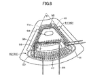
- FIG. 8 is a plan view illustrating a part of the inside of a film deposition apparatus according to an embodiment of the present invention.
- FIG. 9 is a perspective view illustrating a part of a faraday shield of a film deposition apparatus according to an embodiment of the present invention.
- FIG. 10 is an exploded perspective view illustrating a side ring of a film deposition apparatus according to an embodiment of the present invention.
- FIG. 11 is a vertical cross-sectional view illustrating a part of a labyrinth structure part of a film deposition apparatus according to an embodiment of the present invention.
- FIG. 12 is a schematic view for describing the flow of gases in a film deposition apparatus according to an embodiment of the present invention.
- FIG. 13 is a schematic view for describing generation of plasma in a film deposition apparatus according to an embodiment of the present invention.
- FIG. 14 is a perspective view illustrating a part of a film deposition apparatus according to another embodiment of the present invention.
- FIG. 15 is a plan view illustrating a part of a film deposition apparatus according to another embodiment of the present invention.
- FIG. 16 is a plan view illustrating a part of a film deposition apparatus according to another embodiment of the present invention.
- FIG. 17 is a plan view illustrating a film deposition apparatus according to another embodiment of the present invention.
- FIGS. 18-20 are vertical cross-sectional views illustrating parts of a film deposition apparatus according to another embodiment of the present invention.
- FIG. 21 is a perspective view illustrating a part of a film deposition apparatus according to another embodiment of the present invention.
- FIG. 22 is a plan view illustrating a part of a film deposition apparatus according to another embodiment of the present invention.
- FIGS. 23-26 are plan views illustrating a faraday shield of a film deposition apparatus according to embodiments of the present invention.
- FIGS. 27-40 are schematic diagram illustrating experiment results obtained by a film deposition apparatus according to embodiments of the present invention.
- the film deposition apparatus 1000 includes a vacuum chamber 1 and a rotation table 2 provided inside the vacuum chamber 1 .
- the plan shape of the vacuum chamber 1 is substantially a circle.
- the center of rotation of the rotation table 2 is located at the center of the vacuum chamber 1 .
- the film deposition apparatus 1000 deposits a thin film(s) by forming plural layers of a reaction product on a surface of a wafer W by using the ALD method and performs plasma modification on the thin film.
- the film deposition apparatus 1000 is configured to prevent the wafer W from being electrically damaged by plasma or to reduce the damage caused by the plasma.
- parts of the film deposition apparatus 1000 are described in further detail.
- the vacuum chamber 1 has a ceiling plate 11 and a chamber main body 12 .
- the ceiling plate 11 is detachably attached to the chamber main body 12 .
- a separation gas supply nozzle 51 for supplying separation gas e.g., N 2 (nitrogen) gas
- the separation gas prevents different process gases from mixing with each other at a center area C inside the vacuum chamber 1 .
- Reference numeral 13 in FIG. 1 represents an annular sealing member (e.g., O-ring) provided on a circumferential edge part of a top surface of the chamber main body 12 .
- the rotation table 2 is fixed to a center part of a core part 21 having a substantially circular cylinder shape.
- a rotation shaft 22 is attached to a bottom surface of the core part 21 and extends in a vertical direction of the vacuum chamber 1 .
- the rotation table 2 is configured to be rotated around a vertical axis (in this embodiment, clockwise direction) by the rotation shaft 22 .
- Reference numeral 23 of FIG. 1 represents a driving part that rotates the rotation shaft 22 around a vertical axis.
- Reference numeral 20 represents a case body in which the rotation shaft 22 and the driving part 23 are installed.
- the case body 20 has a flange part on a top surface of the case body 20 .
- the flange part is hermetically attached to a bottom surface of a bottom surface part 14 of the vacuum chamber 1 .
- a purge gas supply nozzle 72 for supplying purge gas (e.g., N 2 gas) to a bottom area of the rotation table 2 is connected to the case body 20 .
- An annular projection part 12 a is formed at an outer peripheral side of the core part 21 of the bottom surface part 14 of the vacuum chamber 1 , in a manner that the projection part 12 a is positioned in the vicinity of the bottom of the rotation table 2 .
- plural wafers W are placed on corresponding circular recess parts 24 (substrate receiving regions) on a surface part of the rotation table 2 in a rotation direction (circumferential direction) of the rotation table 2 .
- the recess part 24 is set to have a diameter and a depth that allows an upper surface of the wafer W to match an upper surface of the rotation table (area on which no wafer W is placed) when the wafer W is placed (installed) into the recess part 24 .
- the wafer W may have a diameter of, for example, 300 mm.
- the recess part 24 has through-holes (not illustrated) formed at a bottom surface thereof. The through-holes are for allowing, for example, 3 elevation pins, to penetrate therethrough and raise/lower the wafer W from its bottom side.
- five nozzles 31 , 32 , 34 , 41 , 42 are provided at angular intervals along the circumferential direction of the vacuum chamber 1 (rotation direction of the rotation table 2 ) at positions facing the passing areas of the recess parts 24 of the rotation table 2 .
- the nozzles 31 , 32 , 41 , 42 are attached in a manner horizontally extending in a direction from the circumferential wall of the vacuum chamber 1 to the center area C of the vacuum chamber 1 .
- the nozzles 31 , 32 , 34 , 41 , and 42 correspond to a first process gas nozzle 31 , a second process gas nozzle, a plasma generation gas nozzle, a first separation nozzle, and a second separation nozzle, respectively.
- the plasma generation gas nozzle 34 , the first separation gas nozzle 41 , the first process gas nozzle, the second separation gas nozzle 42 , and the second process gas nozzle 32 are arranged in this order along a clockwise direction from a transfer opening 15 (described below).
- a plasma generation part 80 is provided at an upper side of the plasma gas generation nozzle 34 .
- the plasma generation part 80 is for forming gas into plasma.
- the plasma generation part 80 is described in further detail below.
- the first and second process gas nozzles 31 , 32 are also referred to as a first process gas supply part, and a second process gas supply part, respectively.
- the first and second separation gas nozzles are also referred to as a first separation gas supply part and a second separation gas supply part, respectively.
- FIG. 2 illustrates a state where the plasma generation part 80 and the below-describing housing 90 are removed for the mere purpose of making the plasma generation gas nozzle 34 visible.
- FIG. 3 illustrates a state where the plasma generation part 80 and the housing 90 are attached. Further, the plasma generation part 80 in FIG. 1 is schematically illustrated with a dash-dot line.
- Each of the nozzles 31 , 32 , 34 , 41 , 42 is connected to a corresponding gas supply source (not illustrated) via a flow rate adjustment valve. That is, the first process gas nozzle 31 is connected to a gas supply source that supplies a first process gas containing silicon (Si).
- the first process gas may be BTBAS (bis(tertiary-butylamino) silane, SiH 2 (NH—C(CH 3 ) 3 ) 2 ) gas.
- the second process gas nozzle 32 is connected to a gas supply source that supplies, for example, a mixed gas of ozone (O 3 ) gas and oxygen (O 2 ) gas.
- the first and second separation gas nozzles 41 , 42 are connected to a gas supply source that supplies nitrogen (N 2 ) gas, respectively.
- N 2 nitrogen
- the second process gas is described as O 3 gas for the sake of convenience.
- an ozonizer is provided in the second process gas nozzle 32 for generating O 3 gas, the ozonizer is not illustrated.
- Gas ejection holes 32 are formed in plural parts of the gas nozzles 31 , 32 , 34 , 41 , and 42 in the radial direction of the rotation table 2 .
- the gas ejection holes 32 may be formed at equal intervals in the gas nozzles 31 , 32 , 34 , 41 , and 42 .
- the gas ejection holes 32 formed in the gas nozzles 31 , 32 , 41 , and 42 may be provided on the bottom surface of the gas nozzles 31 , 32 , 41 , and 42 .
- the gas ejection holes 32 formed in the gas nozzle 34 i.e. plasma generation gas nozzle
- the ejection holes 32 of the plasma generation gas nozzle 34 face an upstream side relative to the rotation direction of the rotation table 2 (i.e. toward the second process gas nozzle 32 ) but at the same time downward (diagonally downward).
- the reason that the ejection holes 32 of the plasma generation gas nozzle 34 face the aforementioned direction is described below.
- the ejection holes 32 of the plasma generation gas nozzle 34 which are formed along a longitudinal direction of the plasma generation gas nozzle 34 , have a diameter of, for example, 0.3 mm to 0.5 mm.
- the distance between the gas ejection holes of the nozzles 31 , 32 , 34 , 41 , and 42 and the top surface of the rotation table 2 is, for example, approximately 1 to 5 mm.
- the area below the first process gas nozzle 31 is a first process area P 1 at which a gas containing Si is adsorbed to the wafer W.
- the area below the second process gas nozzle 32 is a second process area P 2 at which a reaction is created between the Si containing gas adsorbed to the wafer W and an O 3 gas.
- the first separation gas nozzle 41 is for separating the first process area P 1 from the second process area P 2 , to thereby form a first separation area D 1 .
- the second separation gas nozzle 42 is for separating the second process area P 2 from the first process area P 1 , to thereby form a second separation area D 2 .
- a sector-shaped convex portion 4 is provided in the ceiling plate 11 of the vacuum chamber 1 , as shown in FIGS. 2-3 .
- the first and second separation gas nozzles 41 , 42 are accommodated inside corresponding grooves 43 formed in the convex portions 4 .
- the convex portions 4 have low flat ceiling faces (first ceiling faces) 44 being provided on both sides of each of the first and second separation gas nozzles 41 , 42 in the outer peripheral direction, and ceiling faces (second ceiling faces) 45 higher than the ceiling faces 44 being provided on both sides of the ceiling faces 44 in the outer peripheral direction of the ceiling faces 44 (see, for example, FIG. 7 ).
- the convex portion 4 has a bent portion that bends in an L-shape at the outer circumferential edge of the convex portion 4 (portion of the outer edge of the vacuum chamber 1 ).
- the bent portion is provided in a manner facing the outer edge surface of the rotation table 2 and having a slight gap between the chamber main body 12 and the bent portion, so that the first and second process gases can be prevented from mixing with each other.
- the plasma generation part 80 is formed by winding an antenna 83 in a coil.
- the antenna 83 may be a metal wire formed of copper (Cu).
- the plasma generation part 80 is provided above the ceiling plate 11 of the vacuum chamber 1 in a manner that the inner area of the vacuum chamber 1 is hermetically sealed (air-tight).
- the antenna 83 is made of a material formed by applying a nickel plating and a metal plating on a copper surface in this order. For example, as illustrated in FIG.
- an opening part 11 a is formed in the ceiling plate 11 toward the upper side of the plasma generation gas nozzle 34 (more specifically, formed in an area beginning from a position slightly upstream of the plasma generation gas nozzle 34 relative to the rotation direction of the rotation table 2 to a position slightly upstream of the first separation area D 1 (located downstream of the plasma generation gas nozzle 34 ).
- the opening part 11 a has an opening in which the opening is a sector-shape from a plane view.
- the opening part 11 a is formed starting from a position separated approximately 60 mm from the rotation center of the rotation table 2 to a position separated approximately 80 mm outward from the outer edge of the rotation table 2 .
- the opening part 11 a has an end (toward the center of the rotation table 2 ) having an arcuate recess shape from a plan view.
- the recess of the end of the opening part 11 a is formed along the outer rim of the labyrinth structure part 110 in a manner avoiding (not interfering with) the labyrinth structure part 110 .
- the opening diameter of the opening part 11 a becomes gradually smaller from the top end of the ceiling plate 11 to the bottom end of the ceiling plate 11 .
- the opening part 11 a may be formed having, for example, 3 steps 11 b throughout the periphery of the opening part 11 a .
- a groove 11 c is formed on a top surface of the lowermost step (opening rim part) of the three steps 11 b throughout the entire periphery of the opening part 11 a as illustrated in FIG. 5 .
- a sealing member (in this embodiment, an O-ring) 11 d is provided inside the groove 11 c . It is, however, to be noted that the groove 11 c and the O-ring 11 d are not illustrated in FIG. 4 .
- the housing 90 is provided in the opening 11 a .
- the housing 90 has a flange part 90 a constituting an upper peripheral rim part of the housing 90 and a recess part 90 b constituting a lower middle part of the housing 90 .
- the flange part 90 a is formed extending horizontally in a flange-like manner throughout the upper periphery of the housing 90 .
- the recess part 90 b is recessed toward the inside of the vacuum chamber 1 .
- the housing 90 is formed of a magnetic permeable material (a material capable of allowing magnetic force to permeate therethrough) including a dielectric material (e.g., quartz). As illustrated in FIG.
- the thickness of the recess part 90 b has a thickness t of, for example, 20 mm.
- the distance between an inner wall surface (toward the center area C) of the housing 90 and the outer rim of the wafer W is 70 mm. Accordingly, an angle ⁇ defined by two sides of the opening part 11 a (one side toward the upstream side of the rotation direction of the rotation table 2 the other side toward the downstream side of the rotation direction of the rotation table 2 ) and a rotation center of the rotation table 2 is, for example, 68 degrees (see, for example, FIG. 8 ).
- the flange part 90 a engages the lowermost step part 11 b . Then, the step part 11 b (ceiling plate 11 ) and the housing 90 are joined together by the O-ring 11 d . Thereby, the step part 11 b (ceiling plate 11 ) and the housing 90 become hermetically sealed (airtight). Further, the internal atmosphere of the vacuum chamber 1 becomes airtight by pressing a pressing member 91 downward to the flange part 90 a (so that pressure is exerted throughout the periphery of the opening part 11 a ) and fastening the pressing member 91 to the ceiling plate 11 with, for example, a bolt (not illustrated).
- the pressure member 91 is a frame having a shape matching the outer rim of the opening part 11 a .
- the distance h between the bottom surface of the housing 90 and the top surface of the wafer W mounted on the rotation table 2 is 4 mm to 60 mm (in this embodiment, 30 mm).
- FIG. 6 is a bottom view of the housing 90 according to an embodiment of the present invention.
- a gas control projecting part (hereinafter also simply referred to as “projecting part”) 92 is formed at a bottom outer rim part of the housing 90 for preventing N 2 gas or O 3 gas from entering an area below the housing 90 .
- the projecting part 92 is formed throughout the periphery of the housing 90 and projects orthogonally to the rotation table 2 located below the housing 90 .
- the plasma generation gas nozzle 34 is installed in an area surrounded by the inner peripheral surface of the projecting part 92 , the bottom surface of the housing 90 , and the top surface of the rotation table 2 .
- Plasma is generated from the gas supplied from the plasma generation gas nozzle 34 in the area below the housing 90 (plasma space 10 ). Accordingly, if N 2 gas enters the area below the housing 90 , NO x gas would be generated by a reaction caused between plasma of N2 gas and plasma of O 3 (O 2 ) gas. The generated NO x gas causes corrosion of the parts and components of the vacuum chamber 1 . Therefore, in order to prevent NO 2 gas from entering the area below the housing 90 , the projecting part 92 is formed on the bottom side of the housing 90 .
- a part of the projecting part 92 toward a base end of the plasma generation gas nozzle 34 (i.e. toward a sidewall of the vacuum chamber 1 ) has an arcuate notch matching the outer shape of the plasma generation gas nozzle 34 .
- the distance d between the bottom surface of the projecting part 92 and the top surface of the rotation table 2 is 0.5 mm to 4 mm (in this embodiment, 2 mm).
- the width of the projecting part 92 is, for example, 10 mm.
- the height of the projecting part 92 is, for example, 28 mm.
- FIG. 7 is a vertical cross-sectional view of the vacuum chamber 7 with respect to the rotation direction of the rotation table 2 .
- the rotation table 2 rotates in a clockwise direction during a film deposition process.
- the rotation of the rotation table 2 causes N 2 gas to flow to the bottom of the housing 90 from the space between the rotation table 2 and the projecting part 92 . Therefore, gas is ejected from the bottom of the housing to the space between the rotation table 2 and the projecting part 92 in order to prevent N 2 gas from entering the bottom of the housing 90 from the space between the rotation table 2 and the projecting part 92 .
- a the plasma generation gas nozzle 34 has an gas ejection hole 33 facing toward the space between the rotation table 2 and the projecting part 92 .
- the plasma generation gas nozzle 34 is positioned so that the gas ejection hole 33 is oriented downward and toward an upstream side of the rotation direction of the rotation table 2 .
- the orientation of the gas ejection hole 33 of the plasma generation gas nozzle 34 relative to a vertical direction is, for example, approximately 45 degrees.
- the O-ring 11 d hermetically seals off the space between the ceiling plate 11 and the housing 90 from the bottom area of the housing 90 (plasma space 10 ). As illustrated in FIG. 5 , the projecting part 92 is formed throughout the periphery of the housing 90 between the plasma space 10 and the O-ring 11 d . In order to prevent plasma from directly contacting the O-ring 11 d , the O-ring 11 d is positioned away from the plasma space 10 .
- the plasma is prevented from reaching the O-ring 11 d because the plasma would have to pass below the projecting part 92 in order to reach the O-ring 11 d but would nevertheless become inactive before reaching the O-ring 11 d.
- a grounded faraday shield 95 is installed inside the housing 90 .
- the faraday shield 95 is formed of a conductive metal plate having a thickness k of approximately 1 mm.
- the faraday shield 95 is formed into a shape matching an inner shape of the housing 90 .
- the faraday shield 95 is formed of a copper plate or a copper plate having its bottom side plated with a nickel (Ni) film or a gold (Au) film.
- the faraday shield 95 includes a horizontal plane 95 a and a vertical plane 95 b .
- the horizontal plane 95 a is formed extending horizontally along the bottom surface of the housing 90 .
- the vertical plane 95 b is formed upright from an outer peripheral rim of the horizontal plane 95 a throughout the periphery of the faraday shield 95 .
- the faraday shield 95 has a substantially sector shape from a plan view.
- the faraday shield 95 may be formed by performing a rolling process on a metal plate.
- the faraday shield 95 may be formed by bending a part of a metal plate corresponding to the outer side of the horizontal plane 95 a.
- support parts 96 are provided extending horizontally from an upper rim of the faraday shield 95 .
- the support parts 96 are positioned on the left and right sides of the faraday shield 95 .
- the faraday shield 95 is installed in the housing 90 , the bottom surface of the faraday shield 95 contacts the top surface of the housing 90 , and the flange part 90 a of the housing 90 supports the support parts 96 .
- An insulation plate 94 is placed on the horizontal plane 95 a for insulating the faraday shield 95 from the plasma generation part 80 mounted above the faraday shield 95 .
- the insulation plate 94 is formed of, for example, quartz.
- the insulation plate 94 may have a thickness of approximately 2 mm.
- Plural slits 97 are formed in the horizontal plane 95 a . The shape of the slits and/or the arrangement slits are described below together with the description of the antenna 83 of the plasma generation part 80 . It is to be noted that the insulation plate 94 is not illustrated in below-described FIGS. 8 and 9 .
- the plasma generation part 80 is installed inside the faraday shield 95 . Accordingly, as illustrated in FIGS. 4 and 5 , the plasma generation part 80 is provided facing the inside of the vacuum chamber 1 (wafer W on the rotation table 2 ) via the housing 90 , the faraday shield 95 , and the insulation plate 94 .
- the antenna 83 of the plasma generation part 80 is wound around a vertical axis.
- two plasma generation parts 80 are provided in the faraday shield 95 .
- the two plasma generation parts 80 may also be indicated as a first plasma generation part 81 and a second plasma generation part 82 . Each of the first and second plasma generation parts 81 , 82 is wound 3 times. As illustrated in FIGS.
- the first plasma generation part 81 has a substantially sector shape matching the inner rim of the housing 90 .
- An end part of the first plasma generation part 81 toward the center area C and an end part of the first plasma generation part 81 toward the outer periphery of the rotation table 2 are positioned closely to the inner wall of the housing 90 , so that plasma can be radiated (supplied) throughout the area between the end part of the first plasma generation part 81 toward the center area C and the end part of the first plasma generation part 81 toward the outer periphery of the rotation table 2 .
- a flow path is provided inside the antenna 83 for allowing cooling water to flow therethrough, the flow path is not illustrated in the drawings.
- the second plasma generation part 82 is for supplying plasma to the wafer W in an outer peripheral area in a radial direction of the rotation table 2 .
- the second plasma generation part 82 is located in an area between a position separated 200 mm from the center of the wafer W mounted on the rotation table 2 in an outer peripheral direction of the rotation table 2 and a position separated 90 mm from the outer rim of the rotation table 2 .
- the circumferential speed is faster at the outer peripheral area of the rotation table 2 than at the center area of the rotation table 2 . Therefore, the amount of plasma supplied to the wafer W may be less at the outer peripheral area of the rotation table 2 than at the center area of the rotation table 2 .
- the second plasma generation part 82 is for equalizing the amount of plasma supplied to the wafer W in the radial direction of the rotation table 2 . That is, the second plasma generation part 82 is for compensating the amount of plasma supplied from the first plasma generation part 81 to the wafer W.
- the antenna 83 of each of the first and the second plasma generation parts 81 , 82 is connected to a high frequency power source 85 via a matching circuit 84 (see, for example, FIG. 3 ).
- the frequency of the high frequency power source 85 is, for example, 13.56 MHz.
- the output voltage of the high frequency power source 85 is, for example, 5000 W. Thereby, the high frequency electric power supplied to each of the first and the second plasma generation parts 81 , 82 can be adjusted.
- the illustrations of the matching circuit 84 and the high frequency power source 85 are simplified in, for example, FIG. 3 .
- Reference numeral 86 in FIGS. 1, 3, and 4 indicates a connection electrode for electrically connecting each of the first and the second plasma generation parts 81 , 82 to the matching circuit 84 and the high frequency power source 85 .
- the slits 97 of the faraday shield 95 are described in detail.
- the slits 97 prevent the elements of electric field from traveling toward the bottom of the wafer W while allowing the elements of the magnetic field to reach the wafer W. If the electric field generated by the first and the second plasma generation part 81 , 82 reaches the wafer W, the electrical wiring inside the wafer W may be electrically damaged by the electric field.
- the faraday shield 95 is formed of a grounded metal plate, not only is the electric field prevented from reaching the wafer W but also the magnetic field is prevented from reaching the wafer W unless the slits 97 are formed in the faraday shield 95 . That is, in a case where a large opening part is formed below the antenna 83 , not only the electric field but also the magnetic field pass through the opening. Accordingly, the slits 97 are formed with a size (measurements) and arranged in a manner described below for blocking the electric field while allowing the magnetic field to pass therethrough.
- the slits 97 are formed perpendicularly intersecting the winding direction of the antenna 83 of the first and the second plasma generation parts 81 , 82 .
- the slits 97 are formed below the antenna 83 of the first and the second plasma generation parts 81 , 82 and arranged along the peripheral direction of the antenna 83 of the first and the second plasma generation parts 81 , 82 . Accordingly, a portion of the slits 97 (provided in a first area in which the antenna 83 is formed along the radial direction of the rotation table 2 ) are arranged in a straight-line or an arc along a tangential direction of the rotation table 2 or the circumferential direction of the rotation table 2 .
- a portion of the slits 97 (provided in a second area in which the antenna 83 is formed in an arcuate manner along the outer rim of the rotation table 2 ) are arranged in a straight-line and oriented in a direction extending from the rotation center of the rotation table 2 to the outer rim of the rotation table 2 .
- a portion of the slits 97 (provided in a third area between the first and second areas at which the antenna 83 bends) are oblique to the peripheral direction of the rotation table 2 and the radial direction of the rotation table 2 , so that the slits 97 perpendicularly intersect the antenna 83 at the bend part of the antenna 83 . Accordingly, as illustrated in FIGS. 8 and 9 , many slits 97 are arranged along the extending direction of the antenna 83 as illustrated in FIGS. 8 and 9 .
- the high frequency power source 85 (having a frequency of 13.56 MHz in this embodiment) is connected to the antenna 83 .
- the wavelength corresponding to the frequency of the high frequency power source 85 is 22 m according to this embodiment.
- the slits 97 are formed so that the width d 1 of each slit 97 is approximately 1/10000 or less than the wavelength of the antenna 83 .
- the width of the slits d 1 ranges from 1 mm to 5 mm (in this embodiment, 2 mm)
- the distance d 2 between adjacent slits 97 ranges from 1 mm to 5 mm (in this embodiment, 2 mm).
- each of the slits 97 is formed having a length of 60 mm as illustrated in FIG. 9 .
- the slits 97 are formed in an area of the faraday shield 95 that starts from a position approximately 30 mm to the right from a right end of the antenna 83 to a position approximately 30 mm to the left from a left end of the antenna 83 .
- an opening part 98 is formed toward the rotation center of the rotation table 2 and another opening part 98 is formed toward the outer periphery of the rotation table 2 . It is to be noted that the slits 97 are not illustrated in FIG. 3 .
- the illustration of the slits 97 are simplified in FIGS. 4 and 5 , approximately 150 slits may be formed in the faraday shield 95 . Further, although the width d 1 of the slits 97 increases the farther away from the opening part 98 , the drawings such as FIGS. 4, 8, and 9 do not illustrate the increasing width of the slits 97 .
- a side ring (cover body) 100 is provided slightly below the rotation table 2 at the outer peripheral side of the rotation table 2 .
- the side ring 100 protects the inner wall of the vacuum chamber 1 from the cleaning gas. That is, without the side ring 100 , an airstream (evacuation airstream) would flow in a horizontal direction through an annular concave airstream path formed between an outer peripheral part of the rotation table 2 and the inner wall of the vacuum chamber 1 .
- the side ring 100 is placed in the airstream path, so that the inner wall of the vacuum chamber 1 is prevented from being exposed to the airstream path as much as possible.
- the first and the second separation areas D 1 , D 2 , the outer rim of the housing 90 are exposed above the side ring 100 .
- a first evacuation port 61 and a second evacuation port 62 are formed at an upper surface of the side ring 100 . As illustrated in FIG. 2 , the first and the second evacuation ports 61 , 62 are separated from each other in a peripheral direction of the rotation table 2 . That is, the first and the second evacuation ports 61 , 62 are formed in correspondence with evacuation ports (not illustrated) provided below the airstream path.
- the first evacuation port 61 is positioned slightly toward the second separation area D 2 in an area substantially between the first process gas nozzle 31 and the second separation area D 2 located downstream of the first process gas nozzle 31 with respect to the rotation direction of the rotation table 2 .
- the second evacuation port 62 is positioned slightly toward the first separation area D 1 in an area substantially between the plasma generation gas nozzle 34 and the first separation area D 1 located downstream of the plasma generation gas nozzle 34 with respect to the rotation direction of the rotation table 2 .
- the first evacuation port 61 is for evacuating the first process gas and the separation gas.
- the second evacuation port 62 is for evacuating the second process gas, the separation gas, and the plasma generation gas.
- the first and the second evacuation ports are connected to an evacuation mechanism such as a vacuum pump 64 via an evacuation pipe 63 of a pressure adjustment valve 65 such as a butterfly valve.
- the housing 90 is formed extending from the center area C of the vacuum chamber 1 to the outer rim of the vacuum chamber 1 , the housing 90 restricts each gas (ejected from an area upstream of the housing 90 with respect to the rotation direction of the rotation table 2 ) flowing toward the second evacuation port 62 . Accordingly, a groove-like gas flow path 101 is formed on an upper surface of the side ring 100 at the outer side of the housing 90 . As illustrated in FIGS. 3 and 10 , the gas flow path 101 is formed in an area starting from a position located approximately 60 mm toward the second process gas nozzle 32 from a rim part (toward the upstream side with respect to the rotation direction of the rotation table 2 ) of the housing 90 and ending at a position of the second evacuation port 62 .
- the gas flow path 101 is formed having an arcuate shape with a thickness of, for example, 30 mm. Accordingly, the gas flow path 101 is formed along the outer rim of the housing 90 and span across the outer rim part of the housing 90 from a plan view.
- the side ring 100 may be covered by a coating material such as alumina or by a quartz cover for attaining corrosion resistance against a fluorine type gas.
- a projecting part 5 is formed at a center part of the bottom surface of the ceiling plate 11 .
- the projecting part 5 continues from the convex portion 4 toward the center area C of the vacuum chamber 1 .
- the projecting part 5 is formed throughout the periphery of the center area C of the vacuum chamber 1 .
- the projecting part 5 has an annular shape.
- the height of the bottom surface of the projecting part 5 relative to the top surface of the rotation table 2 is substantially the same as the height of the bottom surface of the low flat ceiling face 44 of the convex portion 4 relative to the top surface of the rotation table 2 (see, for example, FIGS. 1 and 7 ).
- the labyrinth structure part 110 is provided above the core part 21 for preventing the first and the second process gases from mixing with each other at the center area C of the vacuum chamber 1 .
- the housing 90 is formed extending to the vicinity of the center area C of the vacuum chamber 1 .
- the core part 21 which supports the center part of the rotation table 2 , is formed in a position close to the rotation center of the rotation table 2 but away from the housing 90 . Accordingly, it is easier for the process gases to mix with each other at the center area C of the vacuum chamber 1 than at the outer rim part of the vacuum chamber 1 . Accordingly, the flow of the first and the second processes gases can be blocked by the labyrinth structure part 110 and prevent the first and the second process gases from mixing with each other.
- FIG. 11 is an enlarged view of the labyrinth structure part 110 according to an embodiment of the present invention.
- the labyrinth structure part 110 includes a first wall part 111 extending vertically from the rotation table 2 toward the ceiling plate 11 , a second wall part 112 a , and another second wall part 112 b extending vertically from the ceiling plate 11 toward the rotation table 2 .
- Each of the first and the second wall parts 111 , 112 a , 112 b are formed in the peripheral direction. Further, the first wall part 111 , the second wall part 112 a , and the other second wall part 112 b are alternately arranged in the radial direction of the rotation table 2 .
- the second wall part 112 a , the first wall part 111 , and the other second wall part 112 b are arranged in this order from the side toward the projecting part 5 to the side toward the center area C.
- the second wall part 112 aa bulges more toward the side of the projecting part 5 than the first wall part 111 and the other second wall part 112 b .
- the distance j between the first wall part 111 and the second wall part 112 a / 112 b is 1 mm.
- the distance m between the first wall part 111 and the ceiling plate (also the distance between the second wall part 112 a / 112 b and the core part 21 ) is 1 mm.
- the first process gas flowing from the first process gas nozzle 31 toward the center area C needs to pass the first and the second wall parts 111 , 112 a , 112 b in order to reach the center area C. Accordingly, the flow rate of the first process gas decreases as the first process gas advances toward the center area C. Thus, it becomes difficult for the first process gas to spread. As a result, the first process gas is forced back to the process area P 1 by the separation gas supplied to the center area C before reaching the center area C. Likewise, it becomes difficult for the second process gas flowing toward the center area C to reach the center area C owing to the labyrinth structure part 110 . Hence, the first and the second process gases are prevented from mixing with each other in the center area C.
- N 2 gas being supplied to the center area C from above the center area C, is prevented from rapidly spreading in the peripheral direction. This is because the flow rate of the N 2 gas decreases as the N 2 gas attempts to overcome the first and the second wall parts 111 , 112 a , 112 b .
- the N 2 gas attempts to enter the significantly narrow area between the rotation table 2 and the projecting part 92 , the N 2 gas flows toward a wider area (e.g., first and second process areas P 1 , P 2 ) because the flow rate of the N 2 gas is reduced by the labyrinth structure part 110 . Accordingly, the N 2 gas is prevented from flowing to the area below the housing 90 .
- the N 2 gas is also prevented from flowing to the space at below the housing 90 (plasma space 10 ) because the plasma space 10 has a positive pressure compared to other areas in the vacuum chamber 1 .
- a heater unit (heating mechanism) 7 is provided in the space between the rotation table 2 and the bottom surface part 14 of the vacuum chamber 1 .
- the heater unit 7 heats the wafer W placed on the rotation table 2 via the rotation table 2 .
- the wafer W is heated to a temperature of, for example, 300° C.
- reference numeral 71 a indicates a cover member provided at the side of the heater unit 7
- reference numeral 7 a indicates another cover member for covering a top side of the heater unit 7 .
- plural purge gas supply pipes 73 are provided in a circumferential direction at the bottom surface part 14 of the vacuum chamber 1 below the heater unit 7 .
- the transfer opening 15 is formed in a sidewall of the vacuum chamber 1 for conveying the wafer W between an external transfer arm (not illustrated) and the rotation table 2 .
- the transfer opening 15 can be opened and hermetically sealed (closed) by a gate valve (not illustrated).
- the recess part 24 receives the wafer W transferred from the transfer arm at an area facing the transfer opening 15 .
- elevation pins (not illustrated) for penetrating the recess parts 24 and raising/lowering the recess part 24 and an elevation mechanism of the elevation pins (not illustrated) are provided below the rotation table 2 in an area corresponding to the area in which the wafer W is received.
- the film deposition apparatus 1000 includes a control part 120 including a computer for controlling operations of the entire film deposition apparatus 1000 .
- the control part 120 has a memory (e.g., CPU, central processing unit) in which a program for causing the control part 120 to perform the below-described film deposition process and modification process is stored. A group of steps are assembled to the program for executing the operations of the film deposition apparatus 1000 .
- the program is read out and loaded in the control part 120 from a storage part 121 including a recording medium such as a hard disk, a compact disk, a magneto-optical disk, a memory card, or a flexible disk.
- a gate valve is opened.
- one or more wafers (in this embodiment, 5 wafers) from the transfer opening 15 are mounted to the rotation table 2 .
- a wiring embedding process is performed on the wafers W by using a dry-etching process or a chemical vapor deposition (CVD) process.
- the gate valve is closed so that the inside of the vacuum chamber 1 is evacuated by the vacuum pump 64 .
- the wafers W are heated to, for example, 300° C. by the heater unit 7 while the wafers W are rotated in a clockwise direction at a rate of, for example, 120 rpm by the rotation table 2 .
- Si containing gas and the O 3 gas are ejected from the first and the second process gas nozzles 31 , 32 .
- a mixed gas of Ar gas and O 2 gas e.g., 5 slm
- the separation gas is ejected from the first and the second separation gas nozzles 41 , 42 at a predetermined flow rate.
- N 2 gas is ejected from the separation gas supply pipe 51 and the purge gas supply nozzle 72 at a predetermined flow rate.
- the pressure inside the vacuum chamber 1 is adjusted to, for example, 400-300 Pa (in this embodiment, 500 Pa) by the pressure adjustment valve 65 .
- high frequency power is supplied to the first and the second plasma generation parts 81 , 82 , so the voltage of the first and the second plasma generation parts 81 , 82 becomes, for example, 1500 W and 1000 W, respectively.
- the O 3 gas and the N 2 gas (flowing toward the housing 90 from the upstream side of the housing 90 with respect to the rotation direction of the rotation table 2 ) can be prevented from being disrupted by the housing 90 owing to the gas flow path 101 formed in the side ring 100 at the outer side of the housing 90 . That is, the O 3 gas and the N 2 gas are evacuated by flowing through the gas flow path 101 in a manner avoiding the housing 90 .
- the O 3 gas and the N 2 gas flowing toward the housing 90 from the upstream side of the housing 90 with respect to the rotation direction of the rotation table 2 may attempt to enter the area below the housing 90
- the O 3 gas and the N 2 gas can be blocked out from the housing 90 owing to the projecting part 92 covering the area below the housing 90 and the gas ejection hole 33 of the plasma generation gas nozzle 34 facing obliquely downward toward the upstream side of the rotation direction of the rotation table 2 .
- the plasma generation gas ejected from the plasma generation gas nozzle 34 collides with an area below the projecting part 92 and blocks out the O 3 gas and the N 2 gas attempting to enter the area below the housing 90 .
- the plasma generation gas is deflected by the projecting part 92 toward the downstream side of the rotation direction of the rotation table 2 .
- the plasma space 10 below the housing 90 has a pressure that is approximately 10 Pa more positive than that of the other areas inside the vacuum chamber 1 by providing the projecting part 92 and setting the flow rate of each of the O 3 gas, the N 2 gas, and the plasma generation gas. As a result, the O 3 gas and the N 2 gas are prevented from entering the area below the housing 90 .
- the O 3 gas and the N 2 gas may attempt to enter the center area C
- the O 3 gas and the N 2 gas can be blocked out from the center area C owing to the labyrinth structure part 110 in which the O 3 gas and the N 2 gas are forced backed to their initial first and second process areas P 1 , P 2 by the separation gas supplied to the center area C from above the center area C. Accordingly, the O 3 gas and the N 2 gas can be prevented from mixing with each other in the center area C.
- the N 2 gas ejected from the center area C toward the outer periphery is prevented from entering the area below the housing 90 by the labyrinth structure part 110 .
- the plasma generation gas can be evacuated without mixing with each other. Further, because purge gas is supplied to the area below the rotation table 2 , gases can be prevented from spreading in the area below the rotation table 2 by being forced toward the first and the second evacuation ports 61 , 62 .
- an electric field and a magnetic field are generated in the first and the second plasma generation parts 81 , 82 by high frequency power supplied from the high frequency power source 85 .
- the generated electric field is prevented from reaching the inside of the vacuum chamber 1 (blocked) by being reflected or absorbed (attenuated) by the faraday shield 95 .
- the generated magnetic field passes through the slits 97 formed in the faraday shield 95 and reaches the inside of the vacuum chamber 1 via the bottom surface of the housing 90 .
- FIG. 13 is a schematic diagram illustrating the first and the second plasma generation parts 81 , 82 .
- the first and the second plasma generation parts 81 , 82 , the faraday shield 95 , the housing 90 , and the wafer W are illustrated in an enlarged manner in FIG. 13 .
- the Si containing gas is adsorbed to the surface of the wafer W at the first process area P 1 and then one or more molecular layers of silicon oxide (SiO 2 ) film (thin film component) is formed by oxidizing the Si containing gas adsorbed to the surface of the wafer W at the second process area P 2 .
- SiO 2 silicon oxide
- a reaction product is formed. Impurities such as moisture (OH group) or an organic material may be contained inside the silicon oxide film due to residual groups contained inside the Si containing gas.
- modification of the silicon oxide film is performed by allowing plasma (active species) to contact the surface of the wafer W. More specifically, the impurities may be discharged from the silicon oxide film, or elements inside the silicon oxide film may be rearranged by the plasma colliding against the surface of the wafer W, so that high densification of the silicon oxide film can be achieved.
- the degree of modification tends to become smaller at the outer peripheral part of the rotation table 2 than at the center part of the rotation table 2 by rotating the rotation table 2 because the circumferential speed is faster at the outer peripheral part of the rotation table 2 than at the center part of the rotation table 2 .
- the degree of modification becomes uniform (consistent) in the radial direction of the rotation table 2 .
- the housing 90 is to be installed in the plasma generation part 80 and the faraday shield 95 is to be provided between the plasma generation part 80 and the wafer W.
- the electric field generated by the plasma generation part 80 is blocked off while the magnetic field generated by the plasma generation part 80 reaches the inside of the vacuum chamber 1 by passing through the slits 97 formed in the faraday shield 95 .
- the modification process can be performed by reducing the electric damage to the electric wiring structure inside the wafer W.
- a thin film having a satisfactory film quality and electric characteristic can be obtained.
- the damage (e.g., etching damage) from the plasma to a quartz material such as the housing 90 can be reduced by providing the faraday shield 95 . Accordingly, the lifespan of the quartz material can be increased. Further, generation of contamination can be reduced. Further, the unevenness of the film thickness caused by impurities or the like mixed in the thin film (SiO 2 ) can be prevented.
- the first and the second plasma generation parts 81 , 82 can be placed close to the wafer W. Accordingly, even in a high pressure atmosphere which is high enough to perform film deposition (low degree of vacuum), a modification process can be performed satisfactorily by preventing the ions and radicals inside plasma from being deactivated. Because the projecting part 92 is provided in the housing 90 , the O-ring 11 d can be prevented from being exposed to the plasma space 10 . Accordingly, for example, a fluorine type component contained in the O-ring 11 d can be prevented from entering the wafer W, and the O-ring can attain a long lifespan.
- the projecting part 92 is formed at the bottom surface of the housing 90 , and the gas ejection hole 33 of the plasma generation gas nozzle 34 is formed facing an upstream side with respect to the rotation direction of the rotation table 2 . Accordingly, O 3 gas and N 2 gas can be prevented from entering the area below the housing 90 even in a case where only a small amount of gas is ejected from the plasma generation gas nozzle 34 .
- the pressure of the area in which the plasma generation gas nozzle 34 is provided (plasma space 10 ) is higher than the pressure of other areas in the vacuum chamber 1 (e.g., first and second process areas P 1 , P 2 ). Accordingly, the generation of NOx gas in the plasma space 10 can be prevented.
- the parts and components inside the vacuum chamber 1 can be prevented from being corroded by NOx gas.
- metal contamination of the wafer W can be prevented.
- no additional component e.g., evacuation port, pump
- no separation area D is to be provided between the housing 90 and the nozzle 32 . Accordingly, the configuration of the film deposition apparatus 1000 can be simplified.
- each gas can be prevented from flowing toward the housing 90 and satisfactorily evacuated.
- first and second plasma generation parts 81 , 82 are installed in the housing 90 , the first and the second plasma generation parts 81 , 82 can be placed in an area of atmospheric pressure (area outside the vacuum chamber 1 ). Accordingly, maintenance of the first and the second plasma generation parts 81 , 82 is simplified.
- the end part of the first plasma generation part 81 toward the center area C is separated from the rotation center of the rotation table 2 at a distance equivalent to the thickness of the sidewall of the housing 90 . This makes it difficult for plasma to reach an end part of the wafer W toward the center area C (see below-described simulation results).
- the housing 90 first plasma generation part 81
- the space of the center area C would become narrow and cause process gases to mix with each other at the center area C.
- the labyrinth structure part 11 is formed at the center area C and blocks the path where gases flow toward the center area C. Accordingly, a wide plasma space 10 can be attained in the radial direction of the rotation table 2 while preventing processes gases from mixing with each other at the center area C and preventing the N 2 gas from flowing into the plasma space 10 .
- the degree in which modification is performed on the wafer W can be controlled to be consistent in the radial direction of the rotation table 2 by providing the first and the second plasma generation parts 81 , 82 . Accordingly, the wafer W can attain obtain a thin film having a consistent film property in the in-plane direction of the wafer W.
- the film deposition process of the reaction product and the modification process of the reaction product are performed alternately.
- the modification process may be performed after forming (depositing) a multilayer reaction product having approximately 70 layers (film thickness of approximately 10 nm).
- the supply of high frequency power to the first and the second plasma generation parts 81 , 82 is stopped during a film deposition process of the reaction product by supplying the Si containing gas and the O 3 gas.
- the supply of the Si containing gas and the O 3 gas is stopped after a multilayer reaction product is obtained.
- high frequency power is supplied to the first and the second plasma generation parts 81 , 82 .
- FIGS. 14 and 15 illustrate an embodiment of the present invention in which a single plasma generation part 80 is provided.
- the plasma generation part 80 has a substantially quadrate shape (in this embodiment, a substantially octagonal shape) from a plan view and includes an antenna 83 having a shape matching the substantially quadrate shape of the plasma generation part 80 .
- the width d 1 of the slits 97 increases the farther away from the opening part 98
- FIGS. 14 and 15 do not illustrate the increasing width of the slits 97 .
- FIG. 16 illustrates an embodiment of the present invention in which two plasma generation parts 80 (first and second plasma generation parts 81 , 82 ) having substantially quadrate shapes.
- the first plasma generation part 81 is positioned inward with respect to the radial direction of the rotation table 2 and the second plasma generation part 82 is positioned outward with respect to the radial direction of the rotation table 2 .
- the antenna 83 of the first plasma generation part 81 and the antenna 83 of the second plasma generation part 82 are wound into a shape having area (size) equal to each other.
- FIG. 16 is a schematic plan view (i.e.
- FIG. 17 is also a schematic plan view (i.e. viewed from the ceiling plate 11 ) of the antenna 83 of the first and the second plasma generation parts 81 , 82 according to another embodiment of the present invention.
- the first and second plasma generation parts 81 , 82 also have substantially quadrate shapes. In this embodiment, however, the first plasma generation part 81 has an antenna 83 formed throughout the radial direction of the rotation table 2 whereas the second plasma generation part 82 has an antenna 83 formed in an area toward an outer peripheral part of the rotation table 2 .
- FIG. 18 illustrates an embodiment of the present invention in which the faraday shield 95 is embedded (buried) inside the housing 90 .
- the housing 90 below the plasma generation parts 80 includes a detachable upper end plane. By detaching the upper end plane from the housing 90 , the faraday shield 95 can be installed inside the housing 90 .
- the faraday shield 95 in this embodiment may be provided in other positions as long as the faraday shield 95 is provided between the plasma generation part 80 and the wafer W.
- FIG. 19 illustrates an embodiment of the present invention in which the plasma generation part 80 and the faraday shield 95 are provided above the ceiling plate 11 instead of providing the plasma generation part 80 and the faraday shield 95 inside the housing 90 .
- a portion 11 ′ of the ceiling plate 11 provided below the plasma generation part 80 is formed of a material different from that of another portion 11 ′′ of the ceiling plate 11 .
- the portion 11 ′ of the ceiling plate 11 provided below the plasma generation part 80 is formed of a dielectric material such as quartz.
- a bottom peripheral rim part of the portion 11 ′ of the ceiling plate 11 is hermetically connected to the other portion 11 ′′ of the ceiling plate 11 by an O-ring 11 d formed throughout the peripheral direction.
- FIG. 20 illustrates an embodiment of the present invention in which no side ring 100 is provided in the vacuum chamber 1 .
- the side ring 100 is for preventing cleaning gas from entering an area below the rotation table 2 during a process of cleaning the vacuum chamber 1 . Accordingly, in a case where no cleaning process is performed, the vacuum chamber 1 may be without the side ring 100 .
- FIG. 21 illustrates an embodiment of the present invention in which the antenna 83 is wound in a horizontal direction instead of a vertical direction. More specifically, the antenna 83 is wound around an axis arcuately extending along the radial direction of the rotation table 2 . It is to be noted that parts/components other than the antenna 83 , the slits 97 , and the faraday shield 95 are not illustrated in FIG. 21 .
- a reaction product is deposited on the wafer W by sequentially supplying Si containing gas and O 3 gas to the wafer W in this order. Then, the modification process is performed on the reaction product with the plasma generation part 80 .
- plasma may be generated with the O 3 gas used in depositing the reaction product. That is, in the embodiment illustrated in FIG. 22 , the second process gas nozzle 32 is not provided in the vacuum chamber 1 .
- a reaction product is formed by oxidizing the components of Si containing gas adsorbed on the surface of the wafer W in the plasma space 10 . Then, the modification process is performed on the reaction product in the plasma space 10 .
- the plasma generation gas supplied to the plasma space 10 is also used as the second process gas.
- the plasma generation gas nozzle 34 is used as a second process gas nozzle. Accordingly, no ozonizer as that of the above-described second process gas nozzle 32 is needed, because the components of the Si containing gas adsorbed to the surface of the wafer W are oxidized in the plasma space 10 by the plasma generation gas nozzle 34 . Accordingly, the manufacturing cost of the film deposition apparatus 1000 can be reduced. Further, by generating O 3 gas immediately above the wafer W, the length of the flow path of O 3 gas can be shortened to the extent of the length of the second process gas nozzle 32 . Accordingly, O 3 gas can be prevented from deactivating. As a result, the components of the Si containing gas can be satisfactorily oxidized.
- the material of the faraday shield 95 it is preferable for the material of the faraday shield 95 to have a relative magnetic permeability as low as possible so that magnetic field can permeate through the faraday shield 95 as much as possible.
- the material of the faraday shield 95 may be silver (Ag) or aluminum (Al).
- the number of slits 97 formed in the faraday shield 95 is too small, only a small amount of magnetic field can reach the inside of the vacuum chamber 1 . In a case where the number of slits 97 formed in the faraday shield 95 is too large, it would be difficult to manufacture the faraday shield 95 .
- the number of slits 97 formed in the faraday shield 95 is approximately 100-500 per an antenna 83 having a length of 1 m.
- the plasma generation gas nozzle 34 is positioned in a manner having the gas ejection hole 33 facing the upstream side with respect to the rotation direction of the rotation table 2 .
- the plasma generation gas nozzle 34 may be positioned in a manner having the gas ejection hole 33 facing downward and/or toward the downstream side with respect to the rotation direction of the rotation table 2 .
- the material of the housing 90 may be a plasma-etch resistant material (e.g., alumina (Al 2 O 3 ), yttria) instead of quartz.
- the housing 90 may be formed with, for example, Pyrex (heat resistant glass manufactured by Corning Inc., Registered Trademark) glass coated with a plasma etch resistant material.
- the housing 90 it is preferable for the housing 90 to be formed of a material having a high plasma resistant property and high magnetic permeability (dielectric material).
- the insulation plate 94 is mounting above the faraday shield 95 for insulating the faraday shield 95 and the antenna 83 (plasma generation part 80 ).
- the antenna 83 may be coated with an insulating material such as quartz.
- a silicon oxide film is deposited by using a Si containing gas and O 3 gas.
- a silicon nitride film may be deposited by using a Si containing gas as the first process gas and an ammonia (NH 3 ) gas as the second process gas.
- the plasma generation gas may be, for example, an argon gas, a nitrogen gas, or an ammonia gas.
- a titanium nitride film may be deposited by using a titanium chloride gas (TiCl 2 ) as the first process gas and an ammonia (NH 3 ) gas as the second process gas.
- TiCl 2 titanium chloride gas
- NH 3 ammonia
- a substrate formed of titanium is used as the wafer W, and an argon gas or a nitrogen gas is used as the plasma generation gas.
- a multilayer reaction product may be formed by sequentially supplying 3 or more types of process gases.
- an STO thin multilayer film an oxide film containing Sr and Ti
- the Sr raw material may be, for example, Sr(THD) 2 (strontium-bis-tetra-methyl-heptane-dionato) or Sr (Me 5 Cp) 2 (bis-penta-methyl-cyclo-penta-di-enyl-strontium).
- the Ti raw material may be, for example, Ti(OiPr) 2 (THD) 2 (titanium-bis-iso-propoxide-bis-tetra-methyl-heptane-dionato) or Ti(OiPr) (titanium-tetra-iso-propoxide).
- N2 gas is supplied from the first and the second separation gas nozzles 41 , 42 to the first and the second separation areas D 1 , D 2 .
- a wall part for dividing the first and the second process areas P 1 , P 2 may be provided in the first and second separation areas D 1 , D 2 between the first and the second processes areas P 1 , P 2 .
- the first and the second separation gas nozzles 41 , 42 need be provided in the vacuum chamber 1 .
- the antenna 83 is placed in an area that is hermetically separated from the inside area of the vacuum chamber 1 (that is, placed inside the housing 90 or above the ceiling plate 11 ).
- the antenna 83 may be placed in an area inside the vacuum chamber 1 .
- the antenna 83 may be placed slightly below the bottom surface of the ceiling plate 11 .
- the antenna 83 is coated with a dielectric material such as quartz, so that the antenna 83 can be prevented from being etched by plasma.
- a surface of the faraday shield 95 between the antenna 83 and the wafer W may be coated with a dielectric material such as quartz.
- the antenna may have a configuration other than the above-described coiled configuration.
- the antenna 83 may have a configuration in which a base end of the antenna 83 is hermetically inserted to the inside of the vacuum chamber 1 from the outside of the vacuum chamber 1 and a distal end of the antenna 83 may extend in a straight line toward the center area C.
- a protection cover for protecting an inner wall surface of the vacuum chamber 1 and the ceiling plate 11 from each of the process gases (in a cleaning process, a cleaning gas supplied from the first and the second process gas nozzles 31 , 32 ) is provided in a narrow space in an area more toward the process area than the inner wall surface of the vacuum chamber 1 and the ceiling plate 11 .
- purge gas is supplied to the narrow space of the protection cover from a gas supply part (not illustrated) so that the pressure of the narrow space is slightly positive pressure than a processing atmosphere, a detailed description of the purge gas is omitted.
- the first plasma generation part 81 is formed for generating plasma throughout the radial direction of the rotation table 2 and the second plasma generation part 82 is formed for generating plasma in an area toward the outer periphery of the rotation table 2 , so that the degree of plasma modification performed on the center area of the rotation table 2 and the outer peripheral area of the rotation table can be consistent (uniform).
- the degree of plasma modification can be adjusted by the arrangement of the slits 97 formed in the faraday shield 95 .
- the length of time of irradiating plasma onto the wafer W placed on the rotation table 2 is longer at a part of the wafer W toward the center area C of the rotation table 2 than at a part of the wafer W toward the outer periphery of the rotation table 2 . Accordingly, the degree of plasma modification tends to be larger at the part of the wafer W toward the center area C than at the part of the wafer W toward the outer periphery of the rotation table 2 . Accordingly, as described in the following embodiment of the present invention, the arrangement of the slits 97 of the faraday shield 95 may be adjusted so that the degree of plasma modification can be consistent (uniform) throughout the radial direction of the rotation table 2 .
- the magnetic field having passed through the slits 97 of the faraday shield 95 generates the plasma inside the vacuum chamber 1 . Accordingly, in the following embodiment of the present invention, the area (size) of the openings of the slits 97 is reduced, so that the magnetic field reaching the inside of the vacuum chamber 1 is weaker at the part of the wafer W toward the center area C than at the part of the wafer W toward the outer periphery of the rotation table 2 .
- the antenna 83 has an elongated octagonal shape as illustrated in FIG. 15 , and a single plasma generation part 80 (i.e. only the first plasma generation part 81 ) is provided.
- a single plasma generation part 80 i.e. only the first plasma generation part 81
- the arrangement of slits 97 of FIG. 15 is described with reference to FIG. 23 .
- Each of the slits 97 provided in the longitudinal direction of the antenna 83 i.e. radial direction of the rotation table 2
- Each of the slits 97 provided in the bending part of the antenna 83 i.e.
- FIG. 23 illustrates the antenna 83 with broken lines in FIG. 23 and does not show parts/components other than those of the faraday shield 95 .
- FIGS. 24-26 are illustrated in a similar manner as FIG. 23 .
- FIG. 24 illustrates an embodiment in which supplementary slits 97 a are formed in an area of the faraday shield 95 toward the center area C.
- the supplementary slits 97 a have a length shorter than that of the slits 97 provided in an area toward the outer peripheral part of the rotation table 2 .
- the supplementary slits 97 a are, approximately 20 mm shorter than the slits 97 .
- the supplementary slits 97 are formed extending from a position close to the opening part 98 to a position slightly toward the outer rim of the faraday shield 98 than the antenna 83 . Further, the supplementary slits 97 a and the slits 97 are alternately arranged in the area of the faraday shield 95 toward the center area C of the rotation table 2 . In this embodiment, the supplementary slits 97 a are formed in 9 parts in the area of the faraday shield 95 toward the center of the rotation table 2 .
- the distance d 2 of the intervals between the slits 97 in the area of the faraday shield 95 toward the center area C of the rotation table 2 is longer than that of the intervals between the slits 97 in other areas of the faraday shield 95 to the extent of the supplementary slits 97 a .
- the length of the slits 97 is adjusted to a short length.
- the degree of plasma modification in the radial direction of the rotation table 2 becomes consistent (uniform) by adjusting the arrangement of the slits 97 (see also the results of the following embodiments (experiments)). Accordingly, in a case where there is a desire to attain a consistent degree of plasma modification in the in-plane direction of the wafer W, the faraday shield 95 illustrated in FIG. 24 may be used. In a case where there is a desire to attain a larger degree of plasma modification in the area toward the center of the rotation table 2 than at the area toward the outer rim part of the rotation table 2 , the faraday shield 95 illustrated in FIG. 23 may be used. Thus, a suitable faraday shield 95 can be selected in accordance with the recipe or process to be used.
- both the slits 97 and the supplementary slits 97 a are formed in the area toward the center of the rotation table 2
- the slits in the area toward the center of the rotation table 2 may be replaced with the supplementary slits 97 a
- the supplementary slits 97 a may be formed in 10-50 parts in the faraday shield 95 .
- the cost of the film deposition apparatus 1000 can be reduced by forming the antenna 83 into an elongated substantially octagonal shape. That is, in order for the magnetic field generated in the plasma generating part 80 to reach the inside of the vacuum chamber 1 , the housing 90 is formed of high purity quartz. Further, the housing 90 has a size (from a plan view) larger than that of the antenna 83 so that the quartz housing 90 can be expands covering the bottom of the antenna 83 . Accordingly, the larger the antenna 83 , the larger the housing 90 is to be formed. This may mount up the cost of the film deposition apparatus 1000 (housing 90 ).
- a part of the antenna 83 toward the upstream side with respect to the rotation direction of the rotation table 2 and a part of the antenna toward the downstream side with respect to the rotation direction of the rotation table 2 are positioned closed to each other, so that the size (from the plan view) of the housing 90 can be made as small as possible.
- FIG. 25 illustrates an embodiment of the present invention in which the faraday shield 95 illustrated in FIG. 24 is formed without the supplementary slits 97 a .
- the distance d 2 of the interval between the slits 97 toward the center of the rotation table 2 illustrated in FIG. 25 is the same as the slits 97 toward the center of the rotation table 2 illustrated in FIG. 24 .
- the forming of a slit 97 is skipped so that a slit 97 is formed at every other slit space (instead of forming one slit after another at equal intervals).
- the degree of plasma modification in the radial direction of the rotation table 2 can be uniform.
- the pitch of the slits 97 toward the center of the rotation table 2 may be, for example, approximately 4 mm to 12 mm.
- the slits 97 may become narrower from the center side to the outer rim side of the rotation table 2 .
- FIG. 26 illustrates an embodiment of the present invention in which the width d 1 of the slits 97 toward the center of the rotation table 2 is narrower than the width d 1 of the slits 97 toward the outer rim part of the rotation table 2 .
- the width d 1 of the slits 97 toward the center of the rotation table 2 is, for example, 2 mm to 3 mm.
- 9 slits 97 may be formed toward the center of the rotation table 2 .
- the embodiment illustrated in FIG. 26 can attained the same effects as the above-described embodiments.
- the length of the slits 97 , the pitch of the slits 97 , and the width of the slits 97 are adjusted, respectively.
- the adjustment of the length of the slits 97 , the pitch of the slits 97 , and the width of the slits 97 may be performed in combination.
- the pitch of the slits 97 may be increased and/or the width d 1 of the slits 97 may be reduced.
- the area (size) of the opening of the slits 97 toward the center of the rotation table 2 is smaller than the area (size) of the opening of the slits 97 toward the outer rim part of the rotation table 2 .
- the area (size) of the opening of the slits 97 toward the outer rim part of the rotation table 2 may be increased.
- the length of the slits 97 toward the outer rim part of the rotation table 2 may be more than the length of the slits 97 toward the center of the rotation table 2 and/or the width d 1 of the slits 97 toward the outer rim part of the rotation table 2 may be more than the width d 1 of the slits 97 toward the center of the rotation table 2 .
- the arrangement of the slits 97 toward the center of the rotation table 2 and the arrangement of the slits 97 toward the outer rim part of the rotation table 2 may also be adjusted.
- the pitch between the slits 97 toward the center of the rotation table 2 and the pitch between the slits 97 toward the outer rim part of the rotation table 2 may also be adjusted.
- the slits 97 of the faraday shield 95 may be adjusted in the manner illustrated in FIGS. 24-26 .
- a film deposition apparatus without the labyrinth structure part 110 was evaluated.
- the length of the center area C was extended for preventing the process gases from mixing with each other at the center area C.
- the ends of the opening part 11 a of the ceiling plate 11 and the housing 90 toward the rotation center of the rotation table 2 are positioned approximately 15 mm more toward the outer periphery of the rotation table 2 than the above-described embodiments illustrated in, for example, FIG. 1 .
- a single plasma generation part 80 is provided in the film deposition apparatus in a manner illustrated in FIGS. 14 and 15 .
- a film deposition process and a modification process were performed. It is to be noted that details on the conditions for performing the film deposition process and the modification process in the experiment are omitted.
- the results of experiment 1 are illustrated in FIG. 27 .
- the cycle rate has decreased by performing the plasma modification process compared to a case of not performing the plasma modification process.
- the density of the thin film can be enhanced and a rigid thin film can be obtained by performing the plasma modification process. Accordingly, even in a case where the faraday shield 95 is provided between the plasma generation part 80 and the wafer W, plasma can reach the wafer W.
- the thickness of the wafer W toward the rotation center part and the outer peripheral part of the rotation table 2 is slightly greater than the thickness of an area toward the center of the wafer W (see, for example, the film thickness distribution of a thin film in FIG. 28 ). Accordingly, the strength of the plasma at the rotation center part and the outer peripheral part of the rotation table 2 is less compared to other areas of the rotation table 2 . Accordingly, it is understood that it is preferable for the housing 90 (i.e. providing the labyrinth structure part 110 ) at a position toward the center of the rotation table 2 .
- “cycle rate” indicates the amount of film deposition (film thickness) per single rotation of the rotation table 2 .
- the connecting part between the convex part 4 and projecting part 5 was found to have sufficient strength as illustrated in FIGS. 29 and 30 . Further, the strength of the side ring 100 was also found to have sufficient strength.
- the ceiling plate 11 was found to have sufficient strength.
- the amount of the electrical damage received by the wafer W (more specifically, the gate oxide film of a device formed in the wafer W) in accordance with the providing of the faraday shield 95 was evaluated.
- experiment 3 plural types (in this experiment, 6 types) of wafers having different tolerance against electrical damage were prepared and subjected to plasma irradiation.
- the electrical characteristic of the oxide film is improved by performing the plasma modification process compared to case of not performing the plasma modification process.
- the oxide film exhibited substantially the same electrical characteristic of a thermal oxide film. More specifically, in a case where no plasma modification process is performed, the electric field was 0.4 MV/cm when a current density of 1 ⁇ 10 ⁇ 8 A/cm 2 was applied. In a case where the plasma modification process was performed, the electric field was 8 MV/cm when a current density of 1 ⁇ 10 ⁇ 8 A/cm 2 was applied. Accordingly, it is understood that an oxide film having little impurity density and a small amount of leak current can be obtained by performing the plasma modification process.
- FIG. 33 illustrates the experiment results where the plasma modification process is performed in a batch (in a single time) after depositing the thin film on the wafer W.
- FIG. 34 illustrates the experiment results where the plasma modification process is performed once every rotation of the rotation table 2 .
- the antenna 83 was wound 1 time in a case where no faraday shield 95 was provided, and the antenna 83 was wound approximately 3 times in a case where the faraday shield was provided.
- the wet etching rate of the thin film was observed. That is, the density of the thin film was measured by referring to the wet etching rate. This is because the wet etching rate decreases as the density of the thin film increases, and the wet etching rate increases the more impurities are contained inside the thin film.
- the film thickness of the thin film formed on the wafer was measured after etching the thin film by steeping the wafer in a hydrofluoric acid solution.
- example 31 indicates a case where the plasma modification process was performed per rotation of the rotation table 2
- example 32 indicates a case of forming a multilayer reaction product on the wafer by rotating the rotation table 2 for 9 times, then stopping the supply of each of the process gases, and then performing the plasma modification process on the wafer.
- the antenna 83 was wound 1 time in a case where no faraday shield 95 was provided, and the antenna 83 was wound approximately 3 times in a case where the faraday shield was provided.
- FIG. 36 illustrates distribution of film thickness of a thin film after being subjected to wet etching. It is understood that the film thickness of the thin film hardly changes regardless of whether the faraday shield 95 is provided.
- FIG. 37 illustrates the results of evaluating whether uniformity (consistency) of film thickness can be attained depending on whether the faraday shield 95 is provided.
- the experiment results of the leftmost wafer in the top row of FIG. 37 illustrates a case where no plasma modification was performed
- the experiment results of the middle wafer in the top row of FIG. 37 illustrates a case where plasma modification was performed in a batch without the faraday shield 95 being provided
- the experiment results of the rightmost wafer in the top row of FIG. 37 illustrates a case where plasma modification was performed in a batch with the faraday shield 95 provided.
- the plasma modification process is performed so that the distribution of film thickness is substantially the same as the distribution of film thickness after performing the film deposition process. That is, the distribution of film thickness hardly changes by performing the plasma modification process.
- the experiment results on the left side of FIG. 37 illustrates a case where plasma modification was performed every cycle without the faraday shield 95 provided
- the experiment results on the right side of FIG. 37 illustrates a case where plasma modification was performed every cycle with the faraday shield 95 provided.
- the results illustrated in FIG. 39 was obtained. Accordingly, by using the CCP type plasma generation type having an antenna 83 including a coil structure, the amount of sputter of quartz can be reduced in an order of approximately 100 times.
- FIG. 40 illustrates how the degree of plasma modification is different when comparing a case of using the faraday shield 95 illustrated in FIG. 23 (an embodiment without adjusting the arrangement of slits 97 ) with respect to a case of using the faraday shield 95 illustrated in FIG. 24 (an embodiment using supplementary slits 97 a being shorter than the other slits 97 ) and the faraday shield 95 illustrated in FIG. 25 (an embodiment having the slits 97 arranged with a widened pitch).
- plasma generation gas Ar gas, O 2 gas, and NH 3 gas
Landscapes
- Chemical & Material Sciences (AREA)
- Engineering & Computer Science (AREA)
- General Chemical & Material Sciences (AREA)
- Chemical Kinetics & Catalysis (AREA)
- Materials Engineering (AREA)
- Mechanical Engineering (AREA)
- Metallurgy (AREA)
- Organic Chemistry (AREA)
- Plasma & Fusion (AREA)
- Physics & Mathematics (AREA)
- Analytical Chemistry (AREA)
- Electromagnetism (AREA)
- Chemical Vapour Deposition (AREA)
- Formation Of Insulating Films (AREA)
- Plasma Technology (AREA)
Applications Claiming Priority (6)
| Application Number | Priority Date | Filing Date | Title |
|---|---|---|---|
| JPJP2011-107350 | 2011-05-12 | ||
| JP2011107350 | 2011-05-12 | ||
| JP2011-107350 | 2011-05-12 | ||
| JP2011198396A JP5870568B2 (ja) | 2011-05-12 | 2011-09-12 | 成膜装置、プラズマ処理装置、成膜方法及び記憶媒体 |
| JP2011-198396 | 2011-09-12 | ||
| JPJP2011-198396 | 2011-09-12 |
Publications (2)
| Publication Number | Publication Date |
|---|---|
| US20130149467A1 US20130149467A1 (en) | 2013-06-13 |
| US9932674B2 true US9932674B2 (en) | 2018-04-03 |
Family
ID=47525830
Family Applications (1)
| Application Number | Title | Priority Date | Filing Date |
|---|---|---|---|
| US13/467,324 Active 2034-07-26 US9932674B2 (en) | 2011-05-12 | 2012-05-09 | Film deposition apparatus, film deposition method, and computer-readable recording medium |
Country Status (4)
| Country | Link |
|---|---|
| US (1) | US9932674B2 (ko) |
| JP (1) | JP5870568B2 (ko) |
| KR (1) | KR101563773B1 (ko) |
| TW (1) | TWI509688B (ko) |
Cited By (7)
| Publication number | Priority date | Publication date | Assignee | Title |
|---|---|---|---|---|
| US20170287677A1 (en) * | 2016-03-29 | 2017-10-05 | Tokyo Electron Limited | Plasma processing apparatus and plasma processing method |
| US10998209B2 (en) | 2019-05-31 | 2021-05-04 | Applied Materials, Inc. | Substrate processing platforms including multiple processing chambers |
| US11600507B2 (en) | 2020-09-09 | 2023-03-07 | Applied Materials, Inc. | Pedestal assembly for a substrate processing chamber |
| US11610799B2 (en) | 2020-09-18 | 2023-03-21 | Applied Materials, Inc. | Electrostatic chuck having a heating and chucking capabilities |
| US11674227B2 (en) | 2021-02-03 | 2023-06-13 | Applied Materials, Inc. | Symmetric pump down mini-volume with laminar flow cavity gas injection for high and low pressure |
| US11749542B2 (en) | 2020-07-27 | 2023-09-05 | Applied Materials, Inc. | Apparatus, system, and method for non-contact temperature monitoring of substrate supports |
| US11817331B2 (en) | 2020-07-27 | 2023-11-14 | Applied Materials, Inc. | Substrate holder replacement with protective disk during pasting process |
Families Citing this family (16)
| Publication number | Priority date | Publication date | Assignee | Title |
|---|---|---|---|---|
| JP5131240B2 (ja) * | 2009-04-09 | 2013-01-30 | 東京エレクトロン株式会社 | 成膜装置、成膜方法及び記憶媒体 |
| JP5870568B2 (ja) | 2011-05-12 | 2016-03-01 | 東京エレクトロン株式会社 | 成膜装置、プラズマ処理装置、成膜方法及び記憶媒体 |
| US9282624B2 (en) * | 2011-09-16 | 2016-03-08 | Semes Co., Ltd. | Antenna structure and plasma generating device |
| JP6101083B2 (ja) * | 2013-01-16 | 2017-03-22 | 東京エレクトロン株式会社 | 成膜方法及び成膜装置 |
| CN105051866B (zh) * | 2013-03-15 | 2019-05-17 | 应用材料公司 | 用于旋转压板式ald腔室的等离子体源 |
| JP6135455B2 (ja) * | 2013-10-25 | 2017-05-31 | 東京エレクトロン株式会社 | プラズマ処理装置及びプラズマ処理方法 |
| JP6195528B2 (ja) | 2014-02-19 | 2017-09-13 | 東京エレクトロン株式会社 | プラズマ処理装置及びその運転方法 |
| JP6242288B2 (ja) * | 2014-05-15 | 2017-12-06 | 東京エレクトロン株式会社 | プラズマ処理方法及びプラズマ処理装置 |
| JP6221932B2 (ja) * | 2014-05-16 | 2017-11-01 | 東京エレクトロン株式会社 | 成膜装置 |
| JP5977853B1 (ja) * | 2015-03-20 | 2016-08-24 | 株式会社日立国際電気 | 基板処理装置、半導体装置の製造方法、プログラム及び記録媒体 |
| US11008651B2 (en) * | 2016-04-11 | 2021-05-18 | Spts Technologies Limited | DC magnetron sputtering |
| JP6904150B2 (ja) * | 2017-08-04 | 2021-07-14 | 東京エレクトロン株式会社 | プラズマ処理装置 |
| KR102535194B1 (ko) * | 2018-04-03 | 2023-05-22 | 주성엔지니어링(주) | 기판처리장치 |
| WO2020246523A1 (ja) * | 2019-06-05 | 2020-12-10 | 日新電機株式会社 | プラズマ処理装置 |
| JP7238613B2 (ja) * | 2019-06-05 | 2023-03-14 | 日新電機株式会社 | プラズマ処理装置 |
| JP6910560B1 (ja) * | 2020-01-23 | 2021-07-28 | 株式会社日立ハイテク | プラズマ処理装置およびプラズマ処理装置の運転方法 |
Citations (58)
| Publication number | Priority date | Publication date | Assignee | Title |
|---|---|---|---|---|
| US5234529A (en) | 1991-10-10 | 1993-08-10 | Johnson Wayne L | Plasma generating apparatus employing capacitive shielding and process for using such apparatus |
| US5309063A (en) | 1993-03-04 | 1994-05-03 | David Sarnoff Research Center, Inc. | Inductive coil for inductively coupled plasma production apparatus |
| JPH08213378A (ja) | 1994-11-09 | 1996-08-20 | Hitachi Electron Eng Co Ltd | プラズマcvd装置及び酸化膜の成膜方法 |
| US5560776A (en) * | 1993-09-10 | 1996-10-01 | Kabushiki Kaisha Toshiba | Plasma discharge generating antenna |
| JPH098014A (ja) | 1995-06-15 | 1997-01-10 | Tokyo Electron Ltd | プラズマ成膜方法及びその装置 |
| US5619103A (en) * | 1993-11-02 | 1997-04-08 | Wisconsin Alumni Research Foundation | Inductively coupled plasma generating devices |
| US6000360A (en) * | 1996-07-03 | 1999-12-14 | Tokyo Electron Limited | Plasma processing apparatus |
| US6024826A (en) * | 1996-05-13 | 2000-02-15 | Applied Materials, Inc. | Plasma reactor with heated source of a polymer-hardening precursor material |
| US6149760A (en) * | 1997-10-20 | 2000-11-21 | Tokyo Electron Yamanashi Limited | Plasma processing apparatus |
| JP3144664B2 (ja) | 1992-08-29 | 2001-03-12 | 東京エレクトロン株式会社 | 処理装置及び処理方法 |
| US6213050B1 (en) * | 1998-12-01 | 2001-04-10 | Silicon Genesis Corporation | Enhanced plasma mode and computer system for plasma immersion ion implantation |
| US6232236B1 (en) | 1999-08-03 | 2001-05-15 | Applied Materials, Inc. | Apparatus and method for controlling plasma uniformity in a semiconductor wafer processing system |
| US6287435B1 (en) | 1998-05-06 | 2001-09-11 | Tokyo Electron Limited | Method and apparatus for ionized physical vapor deposition |
| US6322661B1 (en) * | 1999-11-15 | 2001-11-27 | Lam Research Corporation | Method and apparatus for controlling the volume of a plasma |
| US6417626B1 (en) * | 2001-03-01 | 2002-07-09 | Tokyo Electron Limited | Immersed inductively—coupled plasma source |
| US20020092618A1 (en) | 1992-12-01 | 2002-07-18 | Applied Materials, Inc. | Parallel-plate electrode plasma reactor having an inductive antenna coupling power through a parallel plate electrode |
| US6451161B1 (en) | 2000-04-10 | 2002-09-17 | Nano-Architect Research Corporation | Method and apparatus for generating high-density uniform plasma |
| US20020129903A1 (en) * | 2001-03-14 | 2002-09-19 | Applied Materials, Inc. | Variable efficiency faraday shield |
| US20040050329A1 (en) | 2001-02-08 | 2004-03-18 | Taro Ikeda | Plasma processing system and plasma processing method |
| US20040058293A1 (en) | 2002-08-06 | 2004-03-25 | Tue Nguyen | Assembly line processing system |
| US20040163595A1 (en) * | 2003-02-26 | 2004-08-26 | Manabu Edamura | Plasma processing apparatus |
| WO2004090943A2 (en) | 2003-04-01 | 2004-10-21 | Mattson Technology, Inc. | Plasma uniformity |
| US20050022933A1 (en) | 2003-08-01 | 2005-02-03 | Howard Bradley J. | Multi-frequency plasma reactor and method of etching |
| US6869641B2 (en) | 2002-07-03 | 2005-03-22 | Unaxis Balzers Ltd. | Method and apparatus for ALD on a rotary susceptor |
| WO2005052982A1 (en) | 2003-11-19 | 2005-06-09 | Tokyo Electron Limited | Plasma processing system with locally-efficient inductive plasma coupling |
| US6905625B2 (en) | 2001-04-04 | 2005-06-14 | Matsushita Electric Industrial Co., Ltd. | Plasma processing method and apparatus |
| US20060177579A1 (en) * | 2002-09-17 | 2006-08-10 | Shin Cheol H | Method for manufacturing semiconductor device |
| US7153542B2 (en) | 2002-08-06 | 2006-12-26 | Tegal Corporation | Assembly line processing method |
| US20070054044A1 (en) | 2003-07-10 | 2007-03-08 | Sumitomo Titanium | Method for forming metal oxide coating film and vapor deposition apparatus |
| JP2007247066A (ja) | 2006-03-15 | 2007-09-27 | Asm Japan Kk | 回転サセプタを備える半導体処理装置 |
| JP2007305981A (ja) | 2006-04-17 | 2007-11-22 | Applied Materials Inc | 総合プロセスモジュレーション(ipm)hdp−cvdによるギャップ充填のための新規な解決法 |
| US20080026162A1 (en) | 2006-07-29 | 2008-01-31 | Dickey Eric R | Radical-enhanced atomic layer deposition system and method |
| JP2008130651A (ja) | 2006-11-17 | 2008-06-05 | Matsushita Electric Ind Co Ltd | プラズマエッチング装置 |
| JP2008251830A (ja) | 2007-03-30 | 2008-10-16 | Matsushita Electric Ind Co Ltd | プラズマ処理装置 |
| JP2008248281A (ja) | 2007-03-29 | 2008-10-16 | Mitsubishi Heavy Ind Ltd | プラズマ発生装置およびこれを用いた薄膜形成装置 |
| JP2008288437A (ja) | 2007-05-18 | 2008-11-27 | Toshiba Corp | プラズマ処理装置及びプラズマ処理方法 |
| JP2009076876A (ja) | 2007-08-31 | 2009-04-09 | Tokyo Electron Ltd | プラズマ処理装置 |
| US20100062602A1 (en) * | 2005-04-28 | 2010-03-11 | Phyzchemix Corporation | Etching method, method for producing dielectric film of low dielectric constant, method for producing porous member, etching system and thin film forming equipment |
| US20100229797A1 (en) | 2009-03-13 | 2010-09-16 | Tokyo Electron Limited | Film deposition apparatus |
| JP2010212105A (ja) | 2009-03-11 | 2010-09-24 | Emd:Kk | プラズマ処理装置 |
| JP2010239102A (ja) | 2008-06-27 | 2010-10-21 | Tokyo Electron Ltd | 成膜装置、成膜方法及び記憶媒体 |
| JP2010245448A (ja) | 2009-04-09 | 2010-10-28 | Tokyo Electron Ltd | 成膜装置、成膜方法及び記憶媒体 |
| US20100310771A1 (en) | 2009-06-08 | 2010-12-09 | Synos Technology, Inc. | Vapor deposition reactor and method for forming thin film |
| WO2011022612A2 (en) | 2009-08-21 | 2011-02-24 | Mattson Technology, Inc. | Inductive plasma source |
| JP2011040574A (ja) | 2009-08-11 | 2011-02-24 | Tokyo Electron Ltd | 成膜装置、成膜方法及び記憶媒体 |
| US20110048326A1 (en) | 2009-09-01 | 2011-03-03 | Tokyo Electron Limited | Film formation apparatus for semiconductor process |
| JP2011071123A (ja) | 2010-10-29 | 2011-04-07 | Emd:Kk | プラズマ処理装置 |
| WO2011069011A1 (en) | 2009-12-03 | 2011-06-09 | Lam Research Corporation | Small plasma chamber systems and methods |
| CN102110572A (zh) | 2009-12-25 | 2011-06-29 | 东京毅力科创株式会社 | 等离子处理装置 |
| JP2011132589A (ja) | 2009-12-25 | 2011-07-07 | Tokyo Electron Ltd | 成膜装置、成膜方法及び記憶媒体 |
| US20110204023A1 (en) | 2010-02-22 | 2011-08-25 | No-Hyun Huh | Multi inductively coupled plasma reactor and method thereof |
| US20120021252A1 (en) | 2010-07-22 | 2012-01-26 | Synos Technology, Inc. | Treating Surface of Substrate Using Inert Gas Plasma in Atomic Layer Deposition |
| US20120138450A1 (en) | 2010-12-03 | 2012-06-07 | Lam Research Corporation | Immersible Plasma Coil Assembly and Method for Operating the Same |
| US20120273130A1 (en) | 2011-04-28 | 2012-11-01 | Lam Research Corporation | Internal Faraday Shield Having Distributed Chevron Patterns and Correlated Positioning Relative to External Inner and Outer TCP Coil |
| US20130047923A1 (en) | 2011-08-24 | 2013-02-28 | Tokyo Electron Limited | Film deposition apparatus, substrate processing apparatus, and plasma generating device |
| US20130059415A1 (en) | 2011-09-05 | 2013-03-07 | Tokyo Electron Limited | Film deposition apparatus, film deposition method and storage medium |
| US20130130512A1 (en) | 2011-05-18 | 2013-05-23 | Hitoshi Kato | Film deposition method and film deposition apparatus |
| US20130149467A1 (en) | 2011-05-12 | 2013-06-13 | Tokyo Electron Limited | Film deposition apparatus, film deposition method, and computer-readable recording medium |
Family Cites Families (1)
| Publication number | Priority date | Publication date | Assignee | Title |
|---|---|---|---|---|
| JP3150058B2 (ja) * | 1994-12-05 | 2001-03-26 | 東京エレクトロン株式会社 | プラズマ処理装置及びプラズマ処理方法 |
-
2011
- 2011-09-12 JP JP2011198396A patent/JP5870568B2/ja active Active
-
2012
- 2012-05-09 US US13/467,324 patent/US9932674B2/en active Active
- 2012-05-11 TW TW101116768A patent/TWI509688B/zh active
- 2012-05-11 KR KR1020120049992A patent/KR101563773B1/ko active IP Right Grant
Patent Citations (70)
| Publication number | Priority date | Publication date | Assignee | Title |
|---|---|---|---|---|
| US5234529A (en) | 1991-10-10 | 1993-08-10 | Johnson Wayne L | Plasma generating apparatus employing capacitive shielding and process for using such apparatus |
| JP3144664B2 (ja) | 1992-08-29 | 2001-03-12 | 東京エレクトロン株式会社 | 処理装置及び処理方法 |
| US20020092618A1 (en) | 1992-12-01 | 2002-07-18 | Applied Materials, Inc. | Parallel-plate electrode plasma reactor having an inductive antenna coupling power through a parallel plate electrode |
| US5309063A (en) | 1993-03-04 | 1994-05-03 | David Sarnoff Research Center, Inc. | Inductive coil for inductively coupled plasma production apparatus |
| US5560776A (en) * | 1993-09-10 | 1996-10-01 | Kabushiki Kaisha Toshiba | Plasma discharge generating antenna |
| US5619103A (en) * | 1993-11-02 | 1997-04-08 | Wisconsin Alumni Research Foundation | Inductively coupled plasma generating devices |
| JPH08213378A (ja) | 1994-11-09 | 1996-08-20 | Hitachi Electron Eng Co Ltd | プラズマcvd装置及び酸化膜の成膜方法 |
| JPH098014A (ja) | 1995-06-15 | 1997-01-10 | Tokyo Electron Ltd | プラズマ成膜方法及びその装置 |
| US6024826A (en) * | 1996-05-13 | 2000-02-15 | Applied Materials, Inc. | Plasma reactor with heated source of a polymer-hardening precursor material |
| US6000360A (en) * | 1996-07-03 | 1999-12-14 | Tokyo Electron Limited | Plasma processing apparatus |
| US6149760A (en) * | 1997-10-20 | 2000-11-21 | Tokyo Electron Yamanashi Limited | Plasma processing apparatus |
| US6287435B1 (en) | 1998-05-06 | 2001-09-11 | Tokyo Electron Limited | Method and apparatus for ionized physical vapor deposition |
| US6213050B1 (en) * | 1998-12-01 | 2001-04-10 | Silicon Genesis Corporation | Enhanced plasma mode and computer system for plasma immersion ion implantation |
| US6232236B1 (en) | 1999-08-03 | 2001-05-15 | Applied Materials, Inc. | Apparatus and method for controlling plasma uniformity in a semiconductor wafer processing system |
| US6322661B1 (en) * | 1999-11-15 | 2001-11-27 | Lam Research Corporation | Method and apparatus for controlling the volume of a plasma |
| US6451161B1 (en) | 2000-04-10 | 2002-09-17 | Nano-Architect Research Corporation | Method and apparatus for generating high-density uniform plasma |
| US20040050329A1 (en) | 2001-02-08 | 2004-03-18 | Taro Ikeda | Plasma processing system and plasma processing method |
| US20070102119A1 (en) | 2001-02-08 | 2007-05-10 | Taro Ikeda | Plasma processing system and plasma processing method |
| CN1554114A (zh) | 2001-02-08 | 2004-12-08 | 东京毅力科创株式会社 | 等离子体处理装置和等离子体处理方法 |
| US6417626B1 (en) * | 2001-03-01 | 2002-07-09 | Tokyo Electron Limited | Immersed inductively—coupled plasma source |
| US20020129903A1 (en) * | 2001-03-14 | 2002-09-19 | Applied Materials, Inc. | Variable efficiency faraday shield |
| US6905625B2 (en) | 2001-04-04 | 2005-06-14 | Matsushita Electric Industrial Co., Ltd. | Plasma processing method and apparatus |
| US6869641B2 (en) | 2002-07-03 | 2005-03-22 | Unaxis Balzers Ltd. | Method and apparatus for ALD on a rotary susceptor |
| US20040058293A1 (en) | 2002-08-06 | 2004-03-25 | Tue Nguyen | Assembly line processing system |
| US7153542B2 (en) | 2002-08-06 | 2006-12-26 | Tegal Corporation | Assembly line processing method |
| US20060177579A1 (en) * | 2002-09-17 | 2006-08-10 | Shin Cheol H | Method for manufacturing semiconductor device |
| US20040163595A1 (en) * | 2003-02-26 | 2004-08-26 | Manabu Edamura | Plasma processing apparatus |
| JP2006522490A (ja) | 2003-04-01 | 2006-09-28 | マットソン テクノロジイ インコーポレイテッド | プラズマ均一性 |
| WO2004090943A2 (en) | 2003-04-01 | 2004-10-21 | Mattson Technology, Inc. | Plasma uniformity |
| US7232767B2 (en) | 2003-04-01 | 2007-06-19 | Mattson Technology, Inc. | Slotted electrostatic shield modification for improved etch and CVD process uniformity |
| US20070054044A1 (en) | 2003-07-10 | 2007-03-08 | Sumitomo Titanium | Method for forming metal oxide coating film and vapor deposition apparatus |
| US20050022933A1 (en) | 2003-08-01 | 2005-02-03 | Howard Bradley J. | Multi-frequency plasma reactor and method of etching |
| WO2005052982A1 (en) | 2003-11-19 | 2005-06-09 | Tokyo Electron Limited | Plasma processing system with locally-efficient inductive plasma coupling |
| CN1871685A (zh) | 2003-11-19 | 2006-11-29 | 东京毅力科创株式会社 | 具有局部有效电感等离子体耦合的等离子体处理系统 |
| US20100062602A1 (en) * | 2005-04-28 | 2010-03-11 | Phyzchemix Corporation | Etching method, method for producing dielectric film of low dielectric constant, method for producing porous member, etching system and thin film forming equipment |
| JP2007247066A (ja) | 2006-03-15 | 2007-09-27 | Asm Japan Kk | 回転サセプタを備える半導体処理装置 |
| JP2007305981A (ja) | 2006-04-17 | 2007-11-22 | Applied Materials Inc | 総合プロセスモジュレーション(ipm)hdp−cvdによるギャップ充填のための新規な解決法 |
| US20080026162A1 (en) | 2006-07-29 | 2008-01-31 | Dickey Eric R | Radical-enhanced atomic layer deposition system and method |
| JP2008130651A (ja) | 2006-11-17 | 2008-06-05 | Matsushita Electric Ind Co Ltd | プラズマエッチング装置 |
| JP2008248281A (ja) | 2007-03-29 | 2008-10-16 | Mitsubishi Heavy Ind Ltd | プラズマ発生装置およびこれを用いた薄膜形成装置 |
| JP2008251830A (ja) | 2007-03-30 | 2008-10-16 | Matsushita Electric Ind Co Ltd | プラズマ処理装置 |
| JP2008288437A (ja) | 2007-05-18 | 2008-11-27 | Toshiba Corp | プラズマ処理装置及びプラズマ処理方法 |
| JP2009076876A (ja) | 2007-08-31 | 2009-04-09 | Tokyo Electron Ltd | プラズマ処理装置 |
| JP2010239102A (ja) | 2008-06-27 | 2010-10-21 | Tokyo Electron Ltd | 成膜装置、成膜方法及び記憶媒体 |
| JP2010212105A (ja) | 2009-03-11 | 2010-09-24 | Emd:Kk | プラズマ処理装置 |
| US20100229797A1 (en) | 2009-03-13 | 2010-09-16 | Tokyo Electron Limited | Film deposition apparatus |
| TW201102456A (en) | 2009-03-13 | 2011-01-16 | Tokyo Electron Ltd | Film deposition apparatus |
| JP2010245448A (ja) | 2009-04-09 | 2010-10-28 | Tokyo Electron Ltd | 成膜装置、成膜方法及び記憶媒体 |
| US20100310771A1 (en) | 2009-06-08 | 2010-12-09 | Synos Technology, Inc. | Vapor deposition reactor and method for forming thin film |
| JP2011040574A (ja) | 2009-08-11 | 2011-02-24 | Tokyo Electron Ltd | 成膜装置、成膜方法及び記憶媒体 |
| WO2011022612A2 (en) | 2009-08-21 | 2011-02-24 | Mattson Technology, Inc. | Inductive plasma source |
| CN102002685A (zh) | 2009-09-01 | 2011-04-06 | 东京毅力科创株式会社 | 成膜装置和成膜方法 |
| US20110048326A1 (en) | 2009-09-01 | 2011-03-03 | Tokyo Electron Limited | Film formation apparatus for semiconductor process |
| WO2011069011A1 (en) | 2009-12-03 | 2011-06-09 | Lam Research Corporation | Small plasma chamber systems and methods |
| TW201126601A (en) | 2009-12-03 | 2011-08-01 | Lam Res Corp | Small plasma chamber systems and methods |
| JP2011151343A (ja) | 2009-12-25 | 2011-08-04 | Tokyo Electron Ltd | プラズマ処理装置 |
| CN102110572A (zh) | 2009-12-25 | 2011-06-29 | 东京毅力科创株式会社 | 等离子处理装置 |
| US20110155057A1 (en) | 2009-12-25 | 2011-06-30 | Tokyo Electron Limited | Plasma process apparatus |
| JP2011132589A (ja) | 2009-12-25 | 2011-07-07 | Tokyo Electron Ltd | 成膜装置、成膜方法及び記憶媒体 |
| US20110204023A1 (en) | 2010-02-22 | 2011-08-25 | No-Hyun Huh | Multi inductively coupled plasma reactor and method thereof |
| US20120021252A1 (en) | 2010-07-22 | 2012-01-26 | Synos Technology, Inc. | Treating Surface of Substrate Using Inert Gas Plasma in Atomic Layer Deposition |
| JP2011071123A (ja) | 2010-10-29 | 2011-04-07 | Emd:Kk | プラズマ処理装置 |
| US20120138450A1 (en) | 2010-12-03 | 2012-06-07 | Lam Research Corporation | Immersible Plasma Coil Assembly and Method for Operating the Same |
| US20120273130A1 (en) | 2011-04-28 | 2012-11-01 | Lam Research Corporation | Internal Faraday Shield Having Distributed Chevron Patterns and Correlated Positioning Relative to External Inner and Outer TCP Coil |
| US20130149467A1 (en) | 2011-05-12 | 2013-06-13 | Tokyo Electron Limited | Film deposition apparatus, film deposition method, and computer-readable recording medium |
| US20130130512A1 (en) | 2011-05-18 | 2013-05-23 | Hitoshi Kato | Film deposition method and film deposition apparatus |
| US20130047923A1 (en) | 2011-08-24 | 2013-02-28 | Tokyo Electron Limited | Film deposition apparatus, substrate processing apparatus, and plasma generating device |
| JP2013045903A (ja) | 2011-08-24 | 2013-03-04 | Tokyo Electron Ltd | 成膜装置、基板処理装置及びプラズマ発生装置 |
| US20130059415A1 (en) | 2011-09-05 | 2013-03-07 | Tokyo Electron Limited | Film deposition apparatus, film deposition method and storage medium |
| TW201326458A (zh) | 2011-09-05 | 2013-07-01 | Tokyo Electron Ltd | 成膜裝置、成膜方法及記憶媒體 |
Cited By (8)
| Publication number | Priority date | Publication date | Assignee | Title |
|---|---|---|---|---|
| US20170287677A1 (en) * | 2016-03-29 | 2017-10-05 | Tokyo Electron Limited | Plasma processing apparatus and plasma processing method |
| US10153131B2 (en) * | 2016-03-29 | 2018-12-11 | Tokyo Electron Limited | Plasma processing apparatus and plasma processing method |
| US10998209B2 (en) | 2019-05-31 | 2021-05-04 | Applied Materials, Inc. | Substrate processing platforms including multiple processing chambers |
| US11749542B2 (en) | 2020-07-27 | 2023-09-05 | Applied Materials, Inc. | Apparatus, system, and method for non-contact temperature monitoring of substrate supports |
| US11817331B2 (en) | 2020-07-27 | 2023-11-14 | Applied Materials, Inc. | Substrate holder replacement with protective disk during pasting process |
| US11600507B2 (en) | 2020-09-09 | 2023-03-07 | Applied Materials, Inc. | Pedestal assembly for a substrate processing chamber |
| US11610799B2 (en) | 2020-09-18 | 2023-03-21 | Applied Materials, Inc. | Electrostatic chuck having a heating and chucking capabilities |
| US11674227B2 (en) | 2021-02-03 | 2023-06-13 | Applied Materials, Inc. | Symmetric pump down mini-volume with laminar flow cavity gas injection for high and low pressure |
Also Published As
| Publication number | Publication date |
|---|---|
| JP2012253313A (ja) | 2012-12-20 |
| US20130149467A1 (en) | 2013-06-13 |
| TW201310526A (zh) | 2013-03-01 |
| KR20120127281A (ko) | 2012-11-21 |
| JP5870568B2 (ja) | 2016-03-01 |
| KR101563773B1 (ko) | 2015-10-27 |
| TWI509688B (zh) | 2015-11-21 |
Similar Documents
| Publication | Publication Date | Title |
|---|---|---|
| US9932674B2 (en) | Film deposition apparatus, film deposition method, and computer-readable recording medium | |
| US10151031B2 (en) | Method for processing a substrate and substrate processing apparatus | |
| KR101536805B1 (ko) | 성막 장치, 성막 방법 및 기억 매체 | |
| JP5644719B2 (ja) | 成膜装置、基板処理装置及びプラズマ発生装置 | |
| KR101535682B1 (ko) | 활성화 가스 인젝터, 성막 장치 및 성막 방법 | |
| KR101563777B1 (ko) | 성막 장치 및 성막 방법 | |
| US8642487B2 (en) | Film deposition method and film deposition apparatus | |
| US9777369B2 (en) | Method of depositing a film, recording medium, and film deposition apparatus | |
| JP6318869B2 (ja) | 成膜装置 | |
| JP2014017322A (ja) | 成膜装置の運転方法及び成膜装置 | |
| JP2013084730A (ja) | 成膜装置及び基板処理装置 | |
| TWI721227B (zh) | 成膜裝置及成膜方法 | |
| KR101922287B1 (ko) | 플라즈마 처리 장치 및 플라즈마 처리 방법 | |
| CN102776491B (zh) | 成膜装置和成膜方法 | |
| JP5549754B2 (ja) | 成膜装置 |
Legal Events
| Date | Code | Title | Description |
|---|---|---|---|
| AS | Assignment |
Owner name: TOKYO ELECTRON LIMITED, JAPAN Free format text: ASSIGNMENT OF ASSIGNORS INTEREST;ASSIGNORS:KATO, HITOSHI;HISHIYA, KATSUYUKI;KIKUCHI, HIROYUKI;AND OTHERS;REEL/FRAME:028485/0226 Effective date: 20120703 |
|
| STCF | Information on status: patent grant |
Free format text: PATENTED CASE |
|
| MAFP | Maintenance fee payment |
Free format text: PAYMENT OF MAINTENANCE FEE, 4TH YEAR, LARGE ENTITY (ORIGINAL EVENT CODE: M1551); ENTITY STATUS OF PATENT OWNER: LARGE ENTITY Year of fee payment: 4 |